EP3613064B1 - Composant multicouche et procédé de fabrication d'un composant multicouche - Google Patents
Composant multicouche et procédé de fabrication d'un composant multicouche Download PDFInfo
- Publication number
- EP3613064B1 EP3613064B1 EP18719505.2A EP18719505A EP3613064B1 EP 3613064 B1 EP3613064 B1 EP 3613064B1 EP 18719505 A EP18719505 A EP 18719505A EP 3613064 B1 EP3613064 B1 EP 3613064B1
- Authority
- EP
- European Patent Office
- Prior art keywords
- dielectric
- layers
- multilayer component
- ceramic layers
- ceramic
- Prior art date
- Legal status (The legal status is an assumption and is not a legal conclusion. Google has not performed a legal analysis and makes no representation as to the accuracy of the status listed.)
- Active
Links
- 238000004519 manufacturing process Methods 0.000 title claims description 12
- 239000000919 ceramic Substances 0.000 claims description 101
- 239000003989 dielectric material Substances 0.000 claims description 21
- 239000000463 material Substances 0.000 claims description 21
- 238000000034 method Methods 0.000 claims description 14
- 238000007639 printing Methods 0.000 claims description 12
- 239000012876 carrier material Substances 0.000 claims description 9
- 239000007772 electrode material Substances 0.000 claims description 8
- FYYHWMGAXLPEAU-UHFFFAOYSA-N Magnesium Chemical compound [Mg] FYYHWMGAXLPEAU-UHFFFAOYSA-N 0.000 claims description 6
- RTAQQCXQSZGOHL-UHFFFAOYSA-N Titanium Chemical compound [Ti] RTAQQCXQSZGOHL-UHFFFAOYSA-N 0.000 claims description 6
- 229910052749 magnesium Inorganic materials 0.000 claims description 6
- 239000011777 magnesium Substances 0.000 claims description 6
- 238000007650 screen-printing Methods 0.000 claims description 6
- 238000007641 inkjet printing Methods 0.000 claims description 5
- 238000005245 sintering Methods 0.000 claims description 5
- 238000003825 pressing Methods 0.000 claims description 2
- 239000010410 layer Substances 0.000 description 165
- KDLHZDBZIXYQEI-UHFFFAOYSA-N Palladium Chemical compound [Pd] KDLHZDBZIXYQEI-UHFFFAOYSA-N 0.000 description 8
- 230000003071 parasitic effect Effects 0.000 description 6
- 229910052751 metal Inorganic materials 0.000 description 5
- 239000002184 metal Substances 0.000 description 5
- BQCADISMDOOEFD-UHFFFAOYSA-N Silver Chemical compound [Ag] BQCADISMDOOEFD-UHFFFAOYSA-N 0.000 description 4
- 239000002003 electrode paste Substances 0.000 description 4
- 229910052763 palladium Inorganic materials 0.000 description 4
- 238000004080 punching Methods 0.000 description 4
- 229910052709 silver Inorganic materials 0.000 description 4
- 229910010293 ceramic material Inorganic materials 0.000 description 3
- 238000005516 engineering process Methods 0.000 description 3
- 239000000203 mixture Substances 0.000 description 3
- 239000004332 silver Substances 0.000 description 3
- 239000004020 conductor Substances 0.000 description 2
- 239000011888 foil Substances 0.000 description 2
- 238000003475 lamination Methods 0.000 description 2
- 229910052777 Praseodymium Inorganic materials 0.000 description 1
- XLOMVQKBTHCTTD-UHFFFAOYSA-N Zinc monoxide Chemical compound [Zn]=O XLOMVQKBTHCTTD-UHFFFAOYSA-N 0.000 description 1
- 230000005540 biological transmission Effects 0.000 description 1
- 238000010276 construction Methods 0.000 description 1
- 230000001419 dependent effect Effects 0.000 description 1
- 238000010030 laminating Methods 0.000 description 1
- PUDIUYLPXJFUGB-UHFFFAOYSA-N praseodymium atom Chemical compound [Pr] PUDIUYLPXJFUGB-UHFFFAOYSA-N 0.000 description 1
- 230000001681 protective effect Effects 0.000 description 1
- 239000004065 semiconductor Substances 0.000 description 1
- 239000002356 single layer Substances 0.000 description 1
- 239000011343 solid material Substances 0.000 description 1
Images

Classifications
-
- H—ELECTRICITY
- H01—ELECTRIC ELEMENTS
- H01G—CAPACITORS; CAPACITORS, RECTIFIERS, DETECTORS, SWITCHING DEVICES OR LIGHT-SENSITIVE DEVICES, OF THE ELECTROLYTIC TYPE
- H01G4/00—Fixed capacitors; Processes of their manufacture
- H01G4/30—Stacked capacitors
-
- H—ELECTRICITY
- H01—ELECTRIC ELEMENTS
- H01C—RESISTORS
- H01C7/00—Non-adjustable resistors formed as one or more layers or coatings; Non-adjustable resistors made from powdered conducting material or powdered semi-conducting material with or without insulating material
- H01C7/18—Non-adjustable resistors formed as one or more layers or coatings; Non-adjustable resistors made from powdered conducting material or powdered semi-conducting material with or without insulating material comprising a plurality of layers stacked between terminals
-
- H—ELECTRICITY
- H01—ELECTRIC ELEMENTS
- H01C—RESISTORS
- H01C1/00—Details
- H01C1/14—Terminals or tapping points or electrodes specially adapted for resistors; Arrangements of terminals or tapping points or electrodes on resistors
-
- H—ELECTRICITY
- H01—ELECTRIC ELEMENTS
- H01C—RESISTORS
- H01C1/00—Details
- H01C1/14—Terminals or tapping points or electrodes specially adapted for resistors; Arrangements of terminals or tapping points or electrodes on resistors
- H01C1/148—Terminals or tapping points or electrodes specially adapted for resistors; Arrangements of terminals or tapping points or electrodes on resistors the terminals embracing or surrounding the resistive element
-
- H—ELECTRICITY
- H01—ELECTRIC ELEMENTS
- H01C—RESISTORS
- H01C7/00—Non-adjustable resistors formed as one or more layers or coatings; Non-adjustable resistors made from powdered conducting material or powdered semi-conducting material with or without insulating material
- H01C7/10—Non-adjustable resistors formed as one or more layers or coatings; Non-adjustable resistors made from powdered conducting material or powdered semi-conducting material with or without insulating material voltage responsive, i.e. varistors
- H01C7/102—Varistor boundary, e.g. surface layers
-
- H—ELECTRICITY
- H01—ELECTRIC ELEMENTS
- H01C—RESISTORS
- H01C7/00—Non-adjustable resistors formed as one or more layers or coatings; Non-adjustable resistors made from powdered conducting material or powdered semi-conducting material with or without insulating material
- H01C7/10—Non-adjustable resistors formed as one or more layers or coatings; Non-adjustable resistors made from powdered conducting material or powdered semi-conducting material with or without insulating material voltage responsive, i.e. varistors
- H01C7/12—Overvoltage protection resistors
-
- H—ELECTRICITY
- H01—ELECTRIC ELEMENTS
- H01G—CAPACITORS; CAPACITORS, RECTIFIERS, DETECTORS, SWITCHING DEVICES OR LIGHT-SENSITIVE DEVICES, OF THE ELECTROLYTIC TYPE
- H01G4/00—Fixed capacitors; Processes of their manufacture
- H01G4/002—Details
- H01G4/005—Electrodes
- H01G4/012—Form of non-self-supporting electrodes
-
- H—ELECTRICITY
- H01—ELECTRIC ELEMENTS
- H01G—CAPACITORS; CAPACITORS, RECTIFIERS, DETECTORS, SWITCHING DEVICES OR LIGHT-SENSITIVE DEVICES, OF THE ELECTROLYTIC TYPE
- H01G4/00—Fixed capacitors; Processes of their manufacture
- H01G4/002—Details
- H01G4/018—Dielectrics
- H01G4/06—Solid dielectrics
- H01G4/08—Inorganic dielectrics
- H01G4/12—Ceramic dielectrics
- H01G4/1209—Ceramic dielectrics characterised by the ceramic dielectric material
- H01G4/1218—Ceramic dielectrics characterised by the ceramic dielectric material based on titanium oxides or titanates
-
- H—ELECTRICITY
- H01—ELECTRIC ELEMENTS
- H01G—CAPACITORS; CAPACITORS, RECTIFIERS, DETECTORS, SWITCHING DEVICES OR LIGHT-SENSITIVE DEVICES, OF THE ELECTROLYTIC TYPE
- H01G4/00—Fixed capacitors; Processes of their manufacture
- H01G4/002—Details
- H01G4/228—Terminals
- H01G4/236—Terminals leading through the housing, i.e. lead-through
-
- H—ELECTRICITY
- H01—ELECTRIC ELEMENTS
- H01C—RESISTORS
- H01C7/00—Non-adjustable resistors formed as one or more layers or coatings; Non-adjustable resistors made from powdered conducting material or powdered semi-conducting material with or without insulating material
- H01C7/10—Non-adjustable resistors formed as one or more layers or coatings; Non-adjustable resistors made from powdered conducting material or powdered semi-conducting material with or without insulating material voltage responsive, i.e. varistors
- H01C7/1006—Thick film varistors
Definitions
- a multilayer component is described.
- a method for producing a multilayer component is also described.
- An ESD protective component usually consists of a material with a non-linear UI characteristic, to which internal electrodes are connected, which in turn are connected to external electrodes.
- an attempt is made to minimize the overlapping area between the inner electrodes as much as possible while keeping the distance the same.
- an electrical multilayer component is known as an ESD protection component.
- a simple and cost-effective multilayer component should preferably be specified be, which has an ESD protection component with improved properties, such as the lowest capacity.
- a multilayer component has a base body with at least two outer electrodes and at least one first and one second inner electrode, with each inner electrode being electrically conductively connected to an outer electrode.
- the respective inner electrode is electrically conductively connected to the respective outer electrode either directly or via a plated-through hole.
- the multilayer component also has a plurality of ceramic layers, preferably varistor layers.
- the ceramic layers enclose the internal electrodes.
- the inner electrodes are almost completely surrounded by a material from the ceramic layers.
- the respective inner electrode can be contacted freely at least in a contact area with the respective outer electrode.
- the multilayer component also has at least one dielectric layer.
- the multilayer component can also have a plurality of dielectric layers, for example two, five or ten dielectric layers.
- the dielectric layer is arranged between the internal electrodes when viewed along a stacking direction of the ceramic layers.
- the dielectric layer is one of ceramic on at least a portion Printed layers, for example by screen printing or inkjet printing.
- the multilayer component By partially printing a ceramic layer with dielectric material, the overlapping area between the internal electrodes can be reduced in a simple manner, thereby reducing the parasitic capacitance.
- the multilayer component preferably has a capacitance of less than or equal to 0.5 pF, preferably 0.2 pF.
- the structure of the multilayer component can also be easily implemented by simply printing ceramic layers with dielectric material. A simple, cost-effective multilayer component with the lowest capacity is thus made available.
- the dielectric layer has an extension D along the stacking direction of the ceramic layers, where 2 ⁇ m ⁇ D ⁇ 6 ⁇ m. Because the dielectric layer is printed on, a very small thickness of the dielectric layer can be achieved. The material mix in the multi-layer component is thus considerably reduced. Different expansions at boundary layers during the manufacturing process can be avoided.
- the at least one dielectric layer is divided into at least two mutually separated sections in a direction perpendicular to the stacking direction.
- the dielectric layer has a gap.
- the sections are created automatically when the dielectric layer is printed. An additional one after the fact introduced into the dielectric layer, no opening. The portions of the dielectric layer are separated from one another by a material of the ceramic layer. This eliminates the use of backfill materials and an additional filling step. A simplified and cost-effective multilayer component is consequently made available.
- the recess between the sections has an angular or round cross section.
- the geometry of the cutout can be formed in any desired shape and with a high level of accuracy, and can therefore be precisely adapted to the component geometry.
- the at least one dielectric layer includes magnesium titanate.
- the dielectric layer is printed onto the ceramic layer in the form of an ink or paste. Materials are preferably used that can be printed in the form of an ink or paste.
- the dielectric layer is designed and arranged in such a way that it forms an ESD discharge gap together with at least two adjacent ceramic layers and two overlapping internal electrodes.
- the multilayer component has the function of a varistor as an ESD protection component.
- a simple construction of the multilayer component is realized by printing one or more ceramic layers with dielectric in the form of paste or ink.
- the punching of openings in the dielectric layer to produce a reduced overlap area between the internal electrodes by means of complex and expensive laser technology, as in the prior art, is no longer necessary.
- the material mix in the multilayer component is also significantly reduced, the associated problems of different expansions at the boundary layers are eliminated, as is a possible laminating problem when stacking the dielectric layer on the ceramic layer (see prior art) and vice versa.
- the method described above provides a simplified and cost-effective multilayer component with the lowest capacity.
- the figure 1 shows a multilayer component 1 according to the prior art.
- the multilayer component 1 has the function of a varistor as an ESD protection component.
- the multilayer component 1 has, in particular, a base body, on the side faces of which are arranged external electrodes 2, 2', which are electrically conductively connected to internal electrodes 3, 3' located inside the base body.
- the base body of the multilayer component 1 is closed off by a carrier material 8 in the stacking direction.
- the carrier material 8 preferably has at least one dielectric layer.
- the base body also has a ceramic layer 4, in particular a varistor layer.
- the ceramic layer 4 includes a first internal electrode 3.
- the first internal electrode 3 is largely enclosed by the ceramic layer 4.
- the multilayer component 1 also has a further ceramic layer 4', in particular a further varistor layer.
- the further ceramic layer 4' includes a second internal electrode 3', which is largely enclosed by the further ceramic layer 4'.
- a dielectric layer 5 is arranged between the ceramic layer 4 and the further ceramic layer 4'.
- the dielectric layer 5 has an opening or recess 6 .
- the opening 6 is punched into the dielectric layer 5 using laser technology. This can be seen in particular from a round geometry of the opening 6 and from the expansion of the dielectric layer 5 in the stacking direction (thickness of the dielectric layer 5). Laser processing only permits openings 6 with round geometries, the dimensions and target position of which on the dielectric layer 5 vary widely and are difficult to adjust via the laser power. Furthermore, the extent of the dielectric layer 5 in the stacking direction must be large enough so that the opening 6 can be punched at all. For example the dielectric layer 5 has an extension in the stacking direction or thickness of at least 100 ⁇ m.
- the opening 6 is filled with a semiconducting or conducting material 7, e.g. metal.
- a diameter of the opening 6 is between 10 ⁇ m and 50 ⁇ m and thus allows the realization of a defined, small overlapping area of the internal electrodes 3, 3′, as in FIG figure 1 is shown.
- the problem with this solution is the processability of the opening 6, which can only be produced with great effort by means of laser punching and filling the punched hole with a metal paste, for example.
- a metal paste for example.
- an additional dedicated screen printing process is also required.
- the filling of the opening 6 from above only works with great effort in combination with a vacuum from below. This makes the manufacture of the multilayer device 1 complicated and expensive.
- the dielectric layer 5 Before the actual laser stamping process, the dielectric layer 5 must first be pre-pressed so that a stamping process is possible at all. However, the renewed stacking of the already pressed and stamped dielectric layer 5 onto the ceramic layer 4, 4' is almost impossible without lamination problems. If the dielectric layer 5 with the pre-punched and filled opening 6 is nevertheless stacked between the ceramic layers 4, 4', a thermal mismatch between must occur in the subsequent sintering step the materials of the ceramic layers 4, 4', the dielectric layer 5, the outer electrodes 2, 2' and the filling material of the opening 6 are taken into account.
- a length or horizontal extension (extension perpendicular to the stacking direction) of the opening 6 is tied to the thickness of the dielectric (single) layer 5 . If several dielectric layers 5 that have already been punched are stacked on top of each other in order to increase the length of the opening 6, the laser punching must always be carried out with very high precision at the same point in order to avoid misalignment of the openings 6 in the stacked state (see Fig figure 2 ). This drives up the scrap rate and further complicates manufacture.
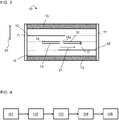
- the multilayer component 10 according to the invention figure 3 solves the problems described above in a simple way.
- the figure 3 1 shows a multilayer component 10.
- the multilayer component 10 has the function of a varistor as an ESD protection component.
- the multilayer component 10 has a base body.
- the multilayer component 10, in particular the base body has at least two external electrodes 11, 11'.
- the outer electrodes 11, 11' are formed on opposite outer surfaces of the base body.
- the multilayer component 10, in particular the base body has at least one first and one second internal electrode 12, 12'.
- the internal electrodes 12, 12' have silver and/or palladium, for example.
- the inner electrodes 12, 12' have an opposite polarity. In each case one inner electrode 12, 12' electrically conductively connected to an outer electrode 11, 11'.
- the multilayer component 10, in particular the base body, has a plurality of ceramic layers 14.
- the ceramic layers 14 have a varistor material.
- the varistor material has zinc oxide (ZnO) or praseodymium (Pr).
- the ceramic layers 14 are stacked one on top of the other to form a stack. In figure 3 the ceramic layers 14 in the stack are indicated by the dashed lines. Consequently, the multilayer component 10 has a stacking direction 20 and a direction 21 perpendicular to the stacking direction 20, as in FIG figure 3 is shown.
- the ceramic layers 14 comprise the internal electrodes 12, 12'.
- the internal electrodes 12, 12' are largely enclosed by the stack of ceramic layers 14.
- FIG. The base body of the multilayer component 10 is closed off by a carrier material 13 in the stacking direction 20, so that the ceramic layers 14, the internal electrodes 12, 12′ and the dielectric layers 15 described below, as in FIG figure 3 shown are arranged in the stacking direction 20 between two layers with the carrier material 13 .
- the carrier material 13 preferably has a dielectric material in order to minimize the parasitic capacitance of the two outer electrodes 11, 11'.
- the multilayer component 10 can, as in figure 3 is shown, also a multiplicity of dielectric layers 15, for example as shown two or more than two, for example five or ten dielectric layers 15.
- the one or more dielectric layers 15 are formed between the internal electrodes 12, 12', viewed along the stacking direction 20 of the ceramic layers 14. In other words, the internal electrodes 12, 12' are formed above and below the one or more dielectric layers 15.
- the one or more dielectric layers 15 include magnesium titanate, for example.
- the one or more dielectric layers 15 together with at least two or more adjacent ceramic layers 14 and two overlapping internal electrodes 12, 12' form an ESD discharge gap.
- the respective dielectric layer 15 is printed onto a ceramic layer 14, in particular onto a partial area of this ceramic layer 14, for example by means of screen printing or inkjet printing.
- the respective dielectric layer 15 is applied to the corresponding ceramic layer 14 in the form of a paste or ink.
- the dielectric material for forming the dielectric layer 15 has no solid material.
- the dielectric layer 15 in the finished multilayer component 10 is therefore a component of the stack of ceramic layers 14.
- the dielectric layer 15 has a very small thickness or dimension D along the stacking direction 20, as shown in FIG figure 3 is indicated.
- the thickness D is between 2 ⁇ m and 6 ⁇ m, the limits being included in each case.
- the multilayer component 10 thus has a multiplicity of dielectric layers 15, the dielectric layers 15 being arranged one above the other between the internal electrodes 12, 12′, viewed along the stacking direction 20 of the ceramic layers 14, each of the dielectric layers 15 being on a partial region one of the ceramic layers 14 is printed on and the dielectric layers 15 each have an extent D of 2 ⁇ m ⁇ D ⁇ 6 ⁇ m along the stacking direction 20 of the ceramic layers 14 .
- the respective dielectric layer 15 is not formed continuously on the respective ceramic layer 14, in particular printed thereon.
- the respective dielectric layer 15 is divided into at least two sections 16 in the direction 21 perpendicular to the stacking direction 20 . These sections 16 are separated from each other. In other words, there is a recess 16a in the dielectric layer 15 between the sections 16.
- the cutout 16a in the dielectric layer 15 is created when the ceramic layer 14 is printed.
- a cutout 16a with a predetermined geometry and size can be produced in a precise manner.
- the recess 16a is comparable to that in connection with figure 1 described opening 6. However, this recess 16a is created automatically when the dielectric layer 15 is printed. Furthermore, filling the recess 16a is also redundant, since the recess 16a between the sections 16 is simply occupied by ceramic material 14.
- the recess 16a between the sections 16 has a variable geometry. In particular, the recess 16a can have a round or an angular cross section. An opening diameter of the recess 16a is between 5 ⁇ m and 40 ⁇ m, for example 20 ⁇ m or 25 ⁇ m.
- the dielectric layer 15 reduces an overlap area between the inner electrodes 12, 12' of opposite polarity in a simple manner. Due to the specially designed dielectric layer 15, the multilayer component 10 has a capacitance of ⁇ 0.5 pF, for example 0.2 pF. A multilayer component 10 with the lowest capacity is thus provided.
- the one or more dielectric layers 15, as in figure 3 is shown, not up to the outer electrodes 11, 11', but are spaced from them. Unlike in the prior art, the one or more dielectric layers 15 therefore do not extend over the entire width from outer electrode to outer electrodes of the multilayer component 10, but rather, as shown, are separated from the outer electrodes 11, 11' by the material of the ceramic layers 14.
- Printing with the material of the one or more dielectric layers that does not extend completely to the edge, ie the outer electrodes can result in shrinkage and detachment of the laminated layers in a further below described sintering can be minimized or completely prevented, since in the edge area, ie adjacent to the outer electrodes, only one ceramic material is present instead of two ceramic materials. In addition, material can be saved compared to the prior art.
- the dielectric layer 5 shown there is thus simply replaced according to the invention by further ceramic layers 14 on which dielectric material is printed.
- the ceramic layers 14 By printing the ceramic layers 14 with a dielectric in the form of a paste or ink, the entire structure of the multilayer component 10 is realized in a significantly simpler manner. The punching of openings 6 using complex and expensive laser technology is no longer necessary.
- the geometry of the cutouts 16a and the spacing of the dielectric layers 15 from the outer electrodes 11, 11' can be formed in any desired geometric shape and with greater precision and can thus be adapted to the component geometry.
- the material mix in the multilayer component 10 is also significantly reduced, the associated problems of different expansions at the boundary layers between dielectric layer 15 and ceramic layer 14 and at the boundary layers of dielectric layer 15 and outer electrode 11, 11' are eliminated, as is a possible lamination problem when stacking the dielectric layer 15 on the ceramic layer 14 and vice versa.
- a first step 101 green ceramic foils (hereafter ceramic layers 14) are provided.
- the ceramic layers 14 have varistor layers.
- a plurality of ceramic layers 14 are provided.
- an electrode material is applied to a surface of part of the ceramic layers 14 to form the internal electrodes 12, 12'.
- the ceramic layers 14 are preferably provided with an electrode paste.
- the green ceramic is coated with the electrode paste in the electrode pattern.
- the electrode paste contains silver and/or palladium.
- the surface of at least one ceramic layer 14 is partially printed with a dielectric material to form at least one dielectric layer 15.
- a dielectric material preferably includes magnesium titanate.
- the dielectric material comes in the form of a paste or ink printed on the ceramic foil. This is done by screen printing or inkjet printing.
- a further step 104 the one or more ceramic layers 14 printed with the dielectric material are arranged (stacked) between the ceramic layers 14 provided with the electrode material. The stack is then pressed to form a base body.
- the outer electrodes 11, 11' are arranged on opposite outer sides of the base body.
- the base body is then sintered (co-sintering).
- the outer electrodes 11, 11' can also be applied to the outer sides only after the base body has been sintered. As a result, a further temperature step is required after the outer electrodes 11, 11' have been applied.
Claims (19)
- Composant multicouche (10) comportant un corps de base comprenant- au moins deux électrodes extérieures (11, 11'),- au moins une première et une deuxième électrode intérieure (12, 12'), chaque électrode intérieure (12, 12') étant reliée électriquement à une électrode extérieure (11, 11'),- une pluralité de couches céramiques (14), les couches céramiques (14) comprenant les électrodes intérieures (12, 12'),- au moins une couche diélectrique (15), la couche diélectrique (15) étant disposée entre les électrodes intérieures (12, 12') lorsqu'elle est observée le long d'une direction d'empilement (20) des couches céramiques (14), et la couche diélectrique (15) étant imprimée sur au moins une partie de l'une des couches céramiques (14), la couche diélectrique étant disposée directement entre deux couches céramiques (14),caractérisé en ce que
la couche diélectrique (15) ne s'étend pas jusqu'aux électrodes extérieures (11, 11'). - Composant multicouche (10) selon la revendication 1, les couches céramiques (14) comportant des couches de varistances.
- Composant multicouche (10) selon la revendication 1 ou 2, la couche diélectrique (14) présentant une extension D le long de la direction d'empilement (20) des couches céramiques (14), avec 2 µm ≤ D ≤ 6 µm.
- Composant multicouche (10) selon l'une des revendications précédentes, la couche diélectrique (15) étant conçue et disposée pour réduire une surface de chevauchement entre des électrodes intérieures (12, 12') de polarités opposées.
- Composant multicouche (10) selon l'une des revendications précédentes, l'au moins une couche diélectrique (15) étant divisée en au moins deux portions (16) séparées l'une de l'autre dans une direction (21) perpendiculaire à la direction d'empilement (20), les portions (16) étant séparées les unes des autres par un matériau de la couche céramique (14) .
- Composant multicouche (10) selon la revendication 5, un évidement (16a) entre les portions (16) ayant une section transversale angulée.
- Composant multicouche (10) selon la revendication 5, un évidement (16a) entre les portions (16) ayant une section transversale ronde.
- Composant multicouche (10) selon l'une des revendications précédentes, l'au moins une couche diélectrique (15) comportant du titanate de magnésium.
- Composant multicouche (10) selon l'une des revendications précédentes, la couche diélectrique (15) étant conçue et disposée de manière à former, conjointement avec au moins deux couches céramiques adjacentes (14) et deux électrodes intérieures (12, 12') qui se chevauchent, un chemin de décharge ESD.
- Composant multicouche (10) selon l'une des revendications précédentes, le composant multicouche (10) ayant la fonction d'une varistance comme composant de protection ESD.
- Composant multicouche (10) selon l'une des revendications précédentes, le composant multicouche (10) ayant une capacité ≤ 0,5 pF.
- Composant multicouche (10) selon l'une des revendications précédentes comprenant un grand nombre de couches diélectriques (15), les couches diélectriques (15) étant disposées, lorsqu'elles sont observées le long d'une direction d'empilement (20) des couches céramiques (14), les unes sur les autres entre les électrodes intérieures (12, 12'), chacune des couches diélectriques (15) étant imprimée sur une zone respective de l'une des couches céramiques (14) et les couches diélectriques (15) présentant chacune une extension D, avec 2 µm ≤ D ≤ 6 µm, le long de la direction d'empilement (20) des couches céramiques (14) .
- Composant multicouche (10) selon l'une des revendications précédentes, le corps de base du composant multicouche (10) étant fermé par un matériau de support diélectrique (13) dans la direction d'empilement (20).
- Procédé de fabrication d'un composant multicouche (1) qui a la fonction d'une varistance comme composant de protection ESD, le procédé comprenant les étapes suivantes:- fournir des couches céramiques (14), les couches céramiques (14) comportant des couches de varistances,- appliquer un matériau d'électrode sur une surface d'une partie des couches céramiques (14) pour former des électrodes intérieures (12, 12'),- imprimer partiellement la surface d'au moins une couche céramique (14) avec un matériau diélectrique pour former au moins une couche diélectrique (15),- empiler la couche céramique (14) imprimée avec le matériau diélectrique entre les couches céramiques (14) pourvues du matériau d'électrode,- presser les couches céramiques (14) pour former un corps de base,- disposer des électrodes extérieures (11, 11') sur des côtés extérieurs opposés du corps de base,- fritter le corps de base,la couche diélectrique étant disposée directement entre deux couches céramiques (14),caractérisé en ce quela couche diélectrique (15) ne s'étend pas jusqu'aux électrodes extérieures (11, 11').
- Procédé selon la revendication 14,
le matériau diélectrique étant appliqué par sérigraphie ou impression à jet d'encre sur l'au moins une couche céramique (14). - Procédé selon la revendication 14 ou 15,
le matériau diélectrique comportant du titanate de magnésium. - Procédé selon l'une des revendications 14 à 16,
le matériau diélectrique étant appliqué sous forme de pâte ou d'encre sur la couche céramique (14). - Procédé selon l'une des revendications 14 à 17,
la surface d'un grand nombre de couches céramiques (14) étant partiellement imprimée avec le matériau diélectrique de sorte que le composant multicouche comporte un grand nombre de couches diélectriques (15) après l'empilement, les couches diélectriques (15) étant disposées, lorsqu'elles sont vues le long d'une direction d'empilement (20) des couches céramiques (14), les unes sur les autres entre les électrodes intérieures (12, 12'), chacune des couches diélectriques (15) étant imprimée sur une partie respective de l'une des couches céramiques (14) et les couches diélectriques (15) présentant chacune une extension D, avec 2 µm ≤ D ≤ 6 µm, le long de la direction d'empilement (20) des couches céramiques (14) . - Procédé selon l'une des revendications 14 à 18, le corps de base du composant multicouche (10) étant fermé avec un matériau de support diélectrique (13) dans la direction d'empilement (20).
Applications Claiming Priority (2)
| Application Number | Priority Date | Filing Date | Title |
|---|---|---|---|
| DE102017108384.7A DE102017108384A1 (de) | 2017-04-20 | 2017-04-20 | Vielschichtbauelement und Verfahren zur Herstellung eines Vielschichtbauelements |
| PCT/EP2018/059751 WO2018192912A1 (fr) | 2017-04-20 | 2018-04-17 | Composant multicouche et procédé de fabrication d'un composant multicouche |
Publications (2)
| Publication Number | Publication Date |
|---|---|
| EP3613064A1 EP3613064A1 (fr) | 2020-02-26 |
| EP3613064B1 true EP3613064B1 (fr) | 2022-06-01 |
Family
ID=62044696
Family Applications (1)
| Application Number | Title | Priority Date | Filing Date |
|---|---|---|---|
| EP18719505.2A Active EP3613064B1 (fr) | 2017-04-20 | 2018-04-17 | Composant multicouche et procédé de fabrication d'un composant multicouche |
Country Status (6)
| Country | Link |
|---|---|
| US (1) | US11532437B2 (fr) |
| EP (1) | EP3613064B1 (fr) |
| JP (1) | JP6905080B2 (fr) |
| CN (1) | CN110506312B (fr) |
| DE (1) | DE102017108384A1 (fr) |
| WO (1) | WO2018192912A1 (fr) |
Families Citing this family (1)
| Publication number | Priority date | Publication date | Assignee | Title |
|---|---|---|---|---|
| US11776996B2 (en) | 2021-11-29 | 2023-10-03 | Infineon Technologies Ag | ESD protection device with isolation structure layout that minimizes harmonic distortion |
Family Cites Families (18)
| Publication number | Priority date | Publication date | Assignee | Title |
|---|---|---|---|---|
| JPH0648666B2 (ja) * | 1987-09-29 | 1994-06-22 | 三菱マテリアル株式会社 | 積層セラミックコンデンサ及びその製法 |
| US5034850A (en) * | 1990-02-12 | 1991-07-23 | Rogers Corporation | Thin decoupling capacitor for mounting under integrated circuit package |
| JPH09148109A (ja) * | 1995-11-21 | 1997-06-06 | Matsushita Electric Ind Co Ltd | 複合機能電子部品 |
| JP3631341B2 (ja) * | 1996-10-18 | 2005-03-23 | Tdk株式会社 | 積層型複合機能素子およびその製造方法 |
| KR20010078252A (ko) * | 2000-02-03 | 2001-08-20 | 가와다 미쓰구 | 유전체 세라믹 분체, 세라믹 그린 시트, 적층 세라믹콘덴서 및 그 제조 방법 |
| US7489914B2 (en) * | 2003-03-28 | 2009-02-10 | Georgia Tech Research Corporation | Multi-band RF transceiver with passive reuse in organic substrates |
| JP4715248B2 (ja) * | 2005-03-11 | 2011-07-06 | パナソニック株式会社 | 積層セラミック電子部品 |
| JP4483659B2 (ja) * | 2005-04-04 | 2010-06-16 | Tdk株式会社 | 電子部品、誘電体磁器組成物およびその製造方法 |
| DE102006000935B4 (de) * | 2006-01-05 | 2016-03-10 | Epcos Ag | Monolithisches keramisches Bauelement und Verfahren zur Herstellung |
| CN101401172B (zh) * | 2006-03-10 | 2011-01-26 | 卓英社有限公司 | 陶瓷组件元件、陶瓷组件及其制造方法 |
| DE102009007316A1 (de) | 2009-02-03 | 2010-08-05 | Epcos Ag | Elektrisches Vielschichtbauelement |
| DE102009014542B3 (de) | 2009-02-12 | 2010-12-02 | Epcos Ag | Mehrschichtbauelement und Verfahren zur Herstellung |
| DE102009010212B4 (de) * | 2009-02-23 | 2017-12-07 | Epcos Ag | Elektrisches Vielschichtbauelement |
| EP2381451B1 (fr) * | 2010-04-22 | 2018-08-01 | Epcos AG | Procédé de production d'un composant électrique multicouches et composant électrique multicouches |
| JPWO2011152256A1 (ja) * | 2010-06-01 | 2013-07-25 | 株式会社村田製作所 | 高周波モジュール |
| GB2502971B (en) * | 2012-06-11 | 2017-10-04 | Knowles (Uk) Ltd | A capacitive structure |
| US10014843B2 (en) * | 2013-08-08 | 2018-07-03 | Zhuhai Advanced Chip Carriers & Electronic Substrate Solutions Technologies Co. Ltd. | Multilayer electronic structures with embedded filters |
| KR101548859B1 (ko) * | 2014-02-26 | 2015-08-31 | 삼성전기주식회사 | 적층 세라믹 전자부품 및 그 실장 기판 |
-
2017
- 2017-04-20 DE DE102017108384.7A patent/DE102017108384A1/de not_active Withdrawn
-
2018
- 2018-04-17 EP EP18719505.2A patent/EP3613064B1/fr active Active
- 2018-04-17 WO PCT/EP2018/059751 patent/WO2018192912A1/fr unknown
- 2018-04-17 JP JP2019556319A patent/JP6905080B2/ja active Active
- 2018-04-17 US US16/605,693 patent/US11532437B2/en active Active
- 2018-04-17 CN CN201880025940.2A patent/CN110506312B/zh active Active
Also Published As
| Publication number | Publication date |
|---|---|
| WO2018192912A1 (fr) | 2018-10-25 |
| US11532437B2 (en) | 2022-12-20 |
| JP6905080B2 (ja) | 2021-07-21 |
| CN110506312A (zh) | 2019-11-26 |
| DE102017108384A1 (de) | 2018-10-25 |
| US20200126730A1 (en) | 2020-04-23 |
| JP2020517116A (ja) | 2020-06-11 |
| CN110506312B (zh) | 2021-12-28 |
| EP3613064A1 (fr) | 2020-02-26 |
Similar Documents
| Publication | Publication Date | Title |
|---|---|---|
| EP2118912B1 (fr) | Composant multicouche et procédé de production d'un tel composant multicouche | |
| DE112008003104B4 (de) | Keramische Mehrschichtkomponente | |
| EP1597780B1 (fr) | Composant electrique multicouche et empilement de couches | |
| DE4091418C2 (de) | Verfahren zur Herstellung eines Mehrschichtkondensators | |
| EP1008193B1 (fr) | Procede de production d'actionneurs piezo-electriques, et actionneur piezo-electrique | |
| WO2013075798A1 (fr) | Condensateur et procédé de fabrication dudit condensateur | |
| EP1997160B1 (fr) | Actionneur piézoélectrique et procédé de fabrication d'un actionneur piézoélectrique | |
| EP2577762B1 (fr) | Procédé de fabrication d'un actionneur piézoélectrique et actionneur piézoélectrique | |
| EP2543085B1 (fr) | Composant piézoélectrique | |
| EP3613064B1 (fr) | Composant multicouche et procédé de fabrication d'un composant multicouche | |
| DE4337749C2 (de) | Verfahren zur Herstellung von Keramik-Multilayern | |
| EP1445795B1 (fr) | Procédé de fabrication de supports de circuits électriques comportant des composants électroniques passifs intégrés | |
| EP3033756B1 (fr) | Procede de fabrication d'un composant multicouche comportant un element de mise en contact exterieur | |
| EP3433911B1 (fr) | Procédé de fabrication d'un parafoudre et parafoudre | |
| DE102016108604A1 (de) | Vielschichtbauelement und Verfahren zur Herstellung eines Vielschichtbauelements | |
| DE102012110556B4 (de) | Vielschichtbauelement und Verfahren zu dessen Herstellung | |
| WO2005067070A1 (fr) | Actionneur avec electrode de raccordement placee interieurement, et procede de production d'un tel actionneur | |
| WO2019029920A1 (fr) | Procédé de métallisation d'une carte de circuit imprimé et carte de circuit imprimé correspondante | |
| DE4410753C2 (de) | Kondensator-Array | |
| WO2019029921A1 (fr) | Gabarit d'impression à employer dans un procédé de métallisation d'une carte de circuit imprimé et utilisation d'un tel gabarit d'impression dans un tel procédé | |
| EP3357135A1 (fr) | Parafoudre et procédé de fabrication d'un parafoudre | |
| DE102008042864A1 (de) | Piezoelektrischer Aktor | |
| WO2011101473A1 (fr) | Composant multicouche piézoélectrique et procédé de fabrication d'un composant multicouche piézoélectrique |
Legal Events
| Date | Code | Title | Description |
|---|---|---|---|
| STAA | Information on the status of an ep patent application or granted ep patent |
Free format text: STATUS: UNKNOWN |
|
| STAA | Information on the status of an ep patent application or granted ep patent |
Free format text: STATUS: THE INTERNATIONAL PUBLICATION HAS BEEN MADE |
|
| PUAI | Public reference made under article 153(3) epc to a published international application that has entered the european phase |
Free format text: ORIGINAL CODE: 0009012 |
|
| STAA | Information on the status of an ep patent application or granted ep patent |
Free format text: STATUS: REQUEST FOR EXAMINATION WAS MADE |
|
| 17P | Request for examination filed |
Effective date: 20191009 |
|
| AK | Designated contracting states |
Kind code of ref document: A1 Designated state(s): AL AT BE BG CH CY CZ DE DK EE ES FI FR GB GR HR HU IE IS IT LI LT LU LV MC MK MT NL NO PL PT RO RS SE SI SK SM TR |
|
| AX | Request for extension of the european patent |
Extension state: BA ME |
|
| DAV | Request for validation of the european patent (deleted) | ||
| DAX | Request for extension of the european patent (deleted) | ||
| GRAP | Despatch of communication of intention to grant a patent |
Free format text: ORIGINAL CODE: EPIDOSNIGR1 |
|
| STAA | Information on the status of an ep patent application or granted ep patent |
Free format text: STATUS: GRANT OF PATENT IS INTENDED |
|
| RIC1 | Information provided on ipc code assigned before grant |
Ipc: H01C 1/148 20060101ALI20211125BHEP Ipc: H01C 7/102 20060101ALI20211125BHEP Ipc: H01C 7/18 20060101ALI20211125BHEP Ipc: H01C 7/10 20060101ALI20211125BHEP Ipc: H01C 7/12 20060101ALI20211125BHEP Ipc: H01C 1/14 20060101AFI20211125BHEP |
|
| INTG | Intention to grant announced |
Effective date: 20211222 |
|
| GRAS | Grant fee paid |
Free format text: ORIGINAL CODE: EPIDOSNIGR3 |
|
| GRAA | (expected) grant |
Free format text: ORIGINAL CODE: 0009210 |
|
| STAA | Information on the status of an ep patent application or granted ep patent |
Free format text: STATUS: THE PATENT HAS BEEN GRANTED |
|
| AK | Designated contracting states |
Kind code of ref document: B1 Designated state(s): AL AT BE BG CH CY CZ DE DK EE ES FI FR GB GR HR HU IE IS IT LI LT LU LV MC MK MT NL NO PL PT RO RS SE SI SK SM TR |
|
| REG | Reference to a national code |
Ref country code: GB Ref legal event code: FG4D Free format text: NOT ENGLISH |
|
| REG | Reference to a national code |
Ref country code: AT Ref legal event code: REF Ref document number: 1495956 Country of ref document: AT Kind code of ref document: T Effective date: 20220615 Ref country code: CH Ref legal event code: EP |
|
| REG | Reference to a national code |
Ref country code: IE Ref legal event code: FG4D Free format text: LANGUAGE OF EP DOCUMENT: GERMAN |
|
| REG | Reference to a national code |
Ref country code: DE Ref legal event code: R096 Ref document number: 502018009809 Country of ref document: DE |
|
| REG | Reference to a national code |
Ref country code: LT Ref legal event code: MG9D |
|
| REG | Reference to a national code |
Ref country code: NL Ref legal event code: MP Effective date: 20220601 |
|
| PG25 | Lapsed in a contracting state [announced via postgrant information from national office to epo] |
Ref country code: SE Free format text: LAPSE BECAUSE OF FAILURE TO SUBMIT A TRANSLATION OF THE DESCRIPTION OR TO PAY THE FEE WITHIN THE PRESCRIBED TIME-LIMIT Effective date: 20220601 Ref country code: NO Free format text: LAPSE BECAUSE OF FAILURE TO SUBMIT A TRANSLATION OF THE DESCRIPTION OR TO PAY THE FEE WITHIN THE PRESCRIBED TIME-LIMIT Effective date: 20220901 Ref country code: LT Free format text: LAPSE BECAUSE OF FAILURE TO SUBMIT A TRANSLATION OF THE DESCRIPTION OR TO PAY THE FEE WITHIN THE PRESCRIBED TIME-LIMIT Effective date: 20220601 Ref country code: HR Free format text: LAPSE BECAUSE OF FAILURE TO SUBMIT A TRANSLATION OF THE DESCRIPTION OR TO PAY THE FEE WITHIN THE PRESCRIBED TIME-LIMIT Effective date: 20220601 Ref country code: GR Free format text: LAPSE BECAUSE OF FAILURE TO SUBMIT A TRANSLATION OF THE DESCRIPTION OR TO PAY THE FEE WITHIN THE PRESCRIBED TIME-LIMIT Effective date: 20220902 Ref country code: FI Free format text: LAPSE BECAUSE OF FAILURE TO SUBMIT A TRANSLATION OF THE DESCRIPTION OR TO PAY THE FEE WITHIN THE PRESCRIBED TIME-LIMIT Effective date: 20220601 Ref country code: ES Free format text: LAPSE BECAUSE OF FAILURE TO SUBMIT A TRANSLATION OF THE DESCRIPTION OR TO PAY THE FEE WITHIN THE PRESCRIBED TIME-LIMIT Effective date: 20220601 Ref country code: BG Free format text: LAPSE BECAUSE OF FAILURE TO SUBMIT A TRANSLATION OF THE DESCRIPTION OR TO PAY THE FEE WITHIN THE PRESCRIBED TIME-LIMIT Effective date: 20220901 |
|
| PG25 | Lapsed in a contracting state [announced via postgrant information from national office to epo] |
Ref country code: RS Free format text: LAPSE BECAUSE OF FAILURE TO SUBMIT A TRANSLATION OF THE DESCRIPTION OR TO PAY THE FEE WITHIN THE PRESCRIBED TIME-LIMIT Effective date: 20220601 Ref country code: PL Free format text: LAPSE BECAUSE OF FAILURE TO SUBMIT A TRANSLATION OF THE DESCRIPTION OR TO PAY THE FEE WITHIN THE PRESCRIBED TIME-LIMIT Effective date: 20220601 Ref country code: LV Free format text: LAPSE BECAUSE OF FAILURE TO SUBMIT A TRANSLATION OF THE DESCRIPTION OR TO PAY THE FEE WITHIN THE PRESCRIBED TIME-LIMIT Effective date: 20220601 |
|
| PG25 | Lapsed in a contracting state [announced via postgrant information from national office to epo] |
Ref country code: NL Free format text: LAPSE BECAUSE OF FAILURE TO SUBMIT A TRANSLATION OF THE DESCRIPTION OR TO PAY THE FEE WITHIN THE PRESCRIBED TIME-LIMIT Effective date: 20220601 |
|
| PG25 | Lapsed in a contracting state [announced via postgrant information from national office to epo] |
Ref country code: SM Free format text: LAPSE BECAUSE OF FAILURE TO SUBMIT A TRANSLATION OF THE DESCRIPTION OR TO PAY THE FEE WITHIN THE PRESCRIBED TIME-LIMIT Effective date: 20220601 Ref country code: SK Free format text: LAPSE BECAUSE OF FAILURE TO SUBMIT A TRANSLATION OF THE DESCRIPTION OR TO PAY THE FEE WITHIN THE PRESCRIBED TIME-LIMIT Effective date: 20220601 Ref country code: RO Free format text: LAPSE BECAUSE OF FAILURE TO SUBMIT A TRANSLATION OF THE DESCRIPTION OR TO PAY THE FEE WITHIN THE PRESCRIBED TIME-LIMIT Effective date: 20220601 Ref country code: PT Free format text: LAPSE BECAUSE OF FAILURE TO SUBMIT A TRANSLATION OF THE DESCRIPTION OR TO PAY THE FEE WITHIN THE PRESCRIBED TIME-LIMIT Effective date: 20221003 Ref country code: EE Free format text: LAPSE BECAUSE OF FAILURE TO SUBMIT A TRANSLATION OF THE DESCRIPTION OR TO PAY THE FEE WITHIN THE PRESCRIBED TIME-LIMIT Effective date: 20220601 Ref country code: CZ Free format text: LAPSE BECAUSE OF FAILURE TO SUBMIT A TRANSLATION OF THE DESCRIPTION OR TO PAY THE FEE WITHIN THE PRESCRIBED TIME-LIMIT Effective date: 20220601 |
|
| PG25 | Lapsed in a contracting state [announced via postgrant information from national office to epo] |
Ref country code: IS Free format text: LAPSE BECAUSE OF FAILURE TO SUBMIT A TRANSLATION OF THE DESCRIPTION OR TO PAY THE FEE WITHIN THE PRESCRIBED TIME-LIMIT Effective date: 20221001 |
|
| REG | Reference to a national code |
Ref country code: DE Ref legal event code: R097 Ref document number: 502018009809 Country of ref document: DE |
|
| PG25 | Lapsed in a contracting state [announced via postgrant information from national office to epo] |
Ref country code: AL Free format text: LAPSE BECAUSE OF FAILURE TO SUBMIT A TRANSLATION OF THE DESCRIPTION OR TO PAY THE FEE WITHIN THE PRESCRIBED TIME-LIMIT Effective date: 20220601 |
|
| PLBE | No opposition filed within time limit |
Free format text: ORIGINAL CODE: 0009261 |
|
| STAA | Information on the status of an ep patent application or granted ep patent |
Free format text: STATUS: NO OPPOSITION FILED WITHIN TIME LIMIT |
|
| PG25 | Lapsed in a contracting state [announced via postgrant information from national office to epo] |
Ref country code: DK Free format text: LAPSE BECAUSE OF FAILURE TO SUBMIT A TRANSLATION OF THE DESCRIPTION OR TO PAY THE FEE WITHIN THE PRESCRIBED TIME-LIMIT Effective date: 20220601 |
|
| 26N | No opposition filed |
Effective date: 20230302 |
|
| PG25 | Lapsed in a contracting state [announced via postgrant information from national office to epo] |
Ref country code: SI Free format text: LAPSE BECAUSE OF FAILURE TO SUBMIT A TRANSLATION OF THE DESCRIPTION OR TO PAY THE FEE WITHIN THE PRESCRIBED TIME-LIMIT Effective date: 20220601 |
|
| P01 | Opt-out of the competence of the unified patent court (upc) registered |
Effective date: 20230521 |
|
| PGFP | Annual fee paid to national office [announced via postgrant information from national office to epo] |
Ref country code: DE Payment date: 20230425 Year of fee payment: 6 |
|
| REG | Reference to a national code |
Ref country code: CH Ref legal event code: PL |
|
| GBPC | Gb: european patent ceased through non-payment of renewal fee |
Effective date: 20230417 |
|
| PG25 | Lapsed in a contracting state [announced via postgrant information from national office to epo] |
Ref country code: LU Free format text: LAPSE BECAUSE OF NON-PAYMENT OF DUE FEES Effective date: 20230417 |
|
| REG | Reference to a national code |
Ref country code: BE Ref legal event code: MM Effective date: 20230430 |
|
| PG25 | Lapsed in a contracting state [announced via postgrant information from national office to epo] |
Ref country code: MC Free format text: LAPSE BECAUSE OF FAILURE TO SUBMIT A TRANSLATION OF THE DESCRIPTION OR TO PAY THE FEE WITHIN THE PRESCRIBED TIME-LIMIT Effective date: 20220601 |
|
| PG25 | Lapsed in a contracting state [announced via postgrant information from national office to epo] |
Ref country code: GB Free format text: LAPSE BECAUSE OF NON-PAYMENT OF DUE FEES Effective date: 20230417 |
|
| PG25 | Lapsed in a contracting state [announced via postgrant information from national office to epo] |
Ref country code: MC Free format text: LAPSE BECAUSE OF FAILURE TO SUBMIT A TRANSLATION OF THE DESCRIPTION OR TO PAY THE FEE WITHIN THE PRESCRIBED TIME-LIMIT Effective date: 20220601 Ref country code: LI Free format text: LAPSE BECAUSE OF NON-PAYMENT OF DUE FEES Effective date: 20230430 Ref country code: IT Free format text: LAPSE BECAUSE OF FAILURE TO SUBMIT A TRANSLATION OF THE DESCRIPTION OR TO PAY THE FEE WITHIN THE PRESCRIBED TIME-LIMIT Effective date: 20220601 Ref country code: GB Free format text: LAPSE BECAUSE OF NON-PAYMENT OF DUE FEES Effective date: 20230417 Ref country code: FR Free format text: LAPSE BECAUSE OF NON-PAYMENT OF DUE FEES Effective date: 20230430 Ref country code: CH Free format text: LAPSE BECAUSE OF NON-PAYMENT OF DUE FEES Effective date: 20230430 |
|
| REG | Reference to a national code |
Ref country code: IE Ref legal event code: MM4A |
|
| PG25 | Lapsed in a contracting state [announced via postgrant information from national office to epo] |
Ref country code: BE Free format text: LAPSE BECAUSE OF NON-PAYMENT OF DUE FEES Effective date: 20230430 |