EP3579346B1 - Connecteur enfichable électrique pour cartes de circuits imprimés - Google Patents
Connecteur enfichable électrique pour cartes de circuits imprimés Download PDFInfo
- Publication number
- EP3579346B1 EP3579346B1 EP19177389.4A EP19177389A EP3579346B1 EP 3579346 B1 EP3579346 B1 EP 3579346B1 EP 19177389 A EP19177389 A EP 19177389A EP 3579346 B1 EP3579346 B1 EP 3579346B1
- Authority
- EP
- European Patent Office
- Prior art keywords
- plug connector
- segment
- accordance
- electric plug
- dielectric body
- Prior art date
- Legal status (The legal status is an assumption and is not a legal conclusion. Google has not performed a legal analysis and makes no representation as to the accuracy of the status listed.)
- Active
Links
- 239000004020 conductor Substances 0.000 claims description 72
- 230000004323 axial length Effects 0.000 claims description 6
- 230000007704 transition Effects 0.000 claims description 2
- 230000014759 maintenance of location Effects 0.000 claims 7
- 238000005452 bending Methods 0.000 description 33
- 230000013011 mating Effects 0.000 description 28
- 239000011324 bead Substances 0.000 description 12
- 241000209035 Ilex Species 0.000 description 10
- 238000011161 development Methods 0.000 description 5
- 230000018109 developmental process Effects 0.000 description 5
- 238000005516 engineering process Methods 0.000 description 3
- 230000002093 peripheral effect Effects 0.000 description 3
- 230000000694 effects Effects 0.000 description 2
- 230000015572 biosynthetic process Effects 0.000 description 1
- 230000001419 dependent effect Effects 0.000 description 1
- 230000006866 deterioration Effects 0.000 description 1
- 238000004519 manufacturing process Methods 0.000 description 1
- 239000000463 material Substances 0.000 description 1
- 238000000034 method Methods 0.000 description 1
- 230000005012 migration Effects 0.000 description 1
- 238000013508 migration Methods 0.000 description 1
- 238000007493 shaping process Methods 0.000 description 1
- 230000008054 signal transmission Effects 0.000 description 1
Images


Classifications
-
- H—ELECTRICITY
- H01—ELECTRIC ELEMENTS
- H01R—ELECTRICALLY-CONDUCTIVE CONNECTIONS; STRUCTURAL ASSOCIATIONS OF A PLURALITY OF MUTUALLY-INSULATED ELECTRICAL CONNECTING ELEMENTS; COUPLING DEVICES; CURRENT COLLECTORS
- H01R12/00—Structural associations of a plurality of mutually-insulated electrical connecting elements, specially adapted for printed circuits, e.g. printed circuit boards [PCB], flat or ribbon cables, or like generally planar structures, e.g. terminal strips, terminal blocks; Coupling devices specially adapted for printed circuits, flat or ribbon cables, or like generally planar structures; Terminals specially adapted for contact with, or insertion into, printed circuits, flat or ribbon cables, or like generally planar structures
- H01R12/70—Coupling devices
- H01R12/71—Coupling devices for rigid printing circuits or like structures
- H01R12/712—Coupling devices for rigid printing circuits or like structures co-operating with the surface of the printed circuit or with a coupling device exclusively provided on the surface of the printed circuit
- H01R12/716—Coupling device provided on the PCB
-
- H—ELECTRICITY
- H01—ELECTRIC ELEMENTS
- H01R—ELECTRICALLY-CONDUCTIVE CONNECTIONS; STRUCTURAL ASSOCIATIONS OF A PLURALITY OF MUTUALLY-INSULATED ELECTRICAL CONNECTING ELEMENTS; COUPLING DEVICES; CURRENT COLLECTORS
- H01R12/00—Structural associations of a plurality of mutually-insulated electrical connecting elements, specially adapted for printed circuits, e.g. printed circuit boards [PCB], flat or ribbon cables, or like generally planar structures, e.g. terminal strips, terminal blocks; Coupling devices specially adapted for printed circuits, flat or ribbon cables, or like generally planar structures; Terminals specially adapted for contact with, or insertion into, printed circuits, flat or ribbon cables, or like generally planar structures
- H01R12/50—Fixed connections
- H01R12/51—Fixed connections for rigid printed circuits or like structures
- H01R12/52—Fixed connections for rigid printed circuits or like structures connecting to other rigid printed circuits or like structures
-
- H—ELECTRICITY
- H01—ELECTRIC ELEMENTS
- H01R—ELECTRICALLY-CONDUCTIVE CONNECTIONS; STRUCTURAL ASSOCIATIONS OF A PLURALITY OF MUTUALLY-INSULATED ELECTRICAL CONNECTING ELEMENTS; COUPLING DEVICES; CURRENT COLLECTORS
- H01R12/00—Structural associations of a plurality of mutually-insulated electrical connecting elements, specially adapted for printed circuits, e.g. printed circuit boards [PCB], flat or ribbon cables, or like generally planar structures, e.g. terminal strips, terminal blocks; Coupling devices specially adapted for printed circuits, flat or ribbon cables, or like generally planar structures; Terminals specially adapted for contact with, or insertion into, printed circuits, flat or ribbon cables, or like generally planar structures
- H01R12/70—Coupling devices
- H01R12/7005—Guiding, mounting, polarizing or locking means; Extractors
- H01R12/7011—Locking or fixing a connector to a PCB
-
- H—ELECTRICITY
- H01—ELECTRIC ELEMENTS
- H01R—ELECTRICALLY-CONDUCTIVE CONNECTIONS; STRUCTURAL ASSOCIATIONS OF A PLURALITY OF MUTUALLY-INSULATED ELECTRICAL CONNECTING ELEMENTS; COUPLING DEVICES; CURRENT COLLECTORS
- H01R12/00—Structural associations of a plurality of mutually-insulated electrical connecting elements, specially adapted for printed circuits, e.g. printed circuit boards [PCB], flat or ribbon cables, or like generally planar structures, e.g. terminal strips, terminal blocks; Coupling devices specially adapted for printed circuits, flat or ribbon cables, or like generally planar structures; Terminals specially adapted for contact with, or insertion into, printed circuits, flat or ribbon cables, or like generally planar structures
- H01R12/70—Coupling devices
- H01R12/7082—Coupling device supported only by cooperation with PCB
-
- H—ELECTRICITY
- H01—ELECTRIC ELEMENTS
- H01R—ELECTRICALLY-CONDUCTIVE CONNECTIONS; STRUCTURAL ASSOCIATIONS OF A PLURALITY OF MUTUALLY-INSULATED ELECTRICAL CONNECTING ELEMENTS; COUPLING DEVICES; CURRENT COLLECTORS
- H01R12/00—Structural associations of a plurality of mutually-insulated electrical connecting elements, specially adapted for printed circuits, e.g. printed circuit boards [PCB], flat or ribbon cables, or like generally planar structures, e.g. terminal strips, terminal blocks; Coupling devices specially adapted for printed circuits, flat or ribbon cables, or like generally planar structures; Terminals specially adapted for contact with, or insertion into, printed circuits, flat or ribbon cables, or like generally planar structures
- H01R12/70—Coupling devices
- H01R12/71—Coupling devices for rigid printing circuits or like structures
- H01R12/72—Coupling devices for rigid printing circuits or like structures coupling with the edge of the rigid printed circuits or like structures
- H01R12/73—Coupling devices for rigid printing circuits or like structures coupling with the edge of the rigid printed circuits or like structures connecting to other rigid printed circuits or like structures
- H01R12/732—Printed circuits being in the same plane
-
- H—ELECTRICITY
- H01—ELECTRIC ELEMENTS
- H01R—ELECTRICALLY-CONDUCTIVE CONNECTIONS; STRUCTURAL ASSOCIATIONS OF A PLURALITY OF MUTUALLY-INSULATED ELECTRICAL CONNECTING ELEMENTS; COUPLING DEVICES; CURRENT COLLECTORS
- H01R12/00—Structural associations of a plurality of mutually-insulated electrical connecting elements, specially adapted for printed circuits, e.g. printed circuit boards [PCB], flat or ribbon cables, or like generally planar structures, e.g. terminal strips, terminal blocks; Coupling devices specially adapted for printed circuits, flat or ribbon cables, or like generally planar structures; Terminals specially adapted for contact with, or insertion into, printed circuits, flat or ribbon cables, or like generally planar structures
- H01R12/70—Coupling devices
- H01R12/91—Coupling devices allowing relative movement between coupling parts, e.g. floating or self aligning
-
- H—ELECTRICITY
- H01—ELECTRIC ELEMENTS
- H01R—ELECTRICALLY-CONDUCTIVE CONNECTIONS; STRUCTURAL ASSOCIATIONS OF A PLURALITY OF MUTUALLY-INSULATED ELECTRICAL CONNECTING ELEMENTS; COUPLING DEVICES; CURRENT COLLECTORS
- H01R13/00—Details of coupling devices of the kinds covered by groups H01R12/70 or H01R24/00 - H01R33/00
- H01R13/02—Contact members
- H01R13/15—Pins, blades or sockets having separate spring member for producing or increasing contact pressure
- H01R13/17—Pins, blades or sockets having separate spring member for producing or increasing contact pressure with spring member on the pin
-
- H—ELECTRICITY
- H01—ELECTRIC ELEMENTS
- H01R—ELECTRICALLY-CONDUCTIVE CONNECTIONS; STRUCTURAL ASSOCIATIONS OF A PLURALITY OF MUTUALLY-INSULATED ELECTRICAL CONNECTING ELEMENTS; COUPLING DEVICES; CURRENT COLLECTORS
- H01R24/00—Two-part coupling devices, or either of their cooperating parts, characterised by their overall structure
- H01R24/38—Two-part coupling devices, or either of their cooperating parts, characterised by their overall structure having concentrically or coaxially arranged contacts
- H01R24/40—Two-part coupling devices, or either of their cooperating parts, characterised by their overall structure having concentrically or coaxially arranged contacts specially adapted for high frequency
- H01R24/50—Two-part coupling devices, or either of their cooperating parts, characterised by their overall structure having concentrically or coaxially arranged contacts specially adapted for high frequency mounted on a PCB [Printed Circuit Board]
-
- H—ELECTRICITY
- H01—ELECTRIC ELEMENTS
- H01R—ELECTRICALLY-CONDUCTIVE CONNECTIONS; STRUCTURAL ASSOCIATIONS OF A PLURALITY OF MUTUALLY-INSULATED ELECTRICAL CONNECTING ELEMENTS; COUPLING DEVICES; CURRENT COLLECTORS
- H01R4/00—Electrically-conductive connections between two or more conductive members in direct contact, i.e. touching one another; Means for effecting or maintaining such contact; Electrically-conductive connections having two or more spaced connecting locations for conductors and using contact members penetrating insulation
- H01R4/26—Connections in which at least one of the connecting parts has projections which bite into or engage the other connecting part in order to improve the contact
Definitions
- the invention relates to an electrical connector for printed circuit boards according to the preamble of claim 1 and a connector arrangement with an electrical connector according to the invention and an associated mating connector.
- the invention also relates to a use of the connector arrangement for the electrical connection of two printed circuit boards.
- B2B board-to-board
- a disadvantage of such B2B connectors is their three-part design.
- One possibility to achieve a simplification of the structure that is derived from the EP 2 780 985 B1 consists in providing a coaxial connection element whose outer conductor has a first conductor with a tubular jacket, the ends of which are intended for contact with the two boards and which has openings for tolerance compensation with regard to the distance between the boards, and also the outer conductor a tubular second conductor in electrical contact with the first conductor having a portion of the first conductor and is in axially movable contact with a portion of the first conductor.
- a lateral offset of the printed circuit boards to be connected to one another can only be compensated for with difficulty.
- the invention is based on the object of specifying an improved connector of the type mentioned at the outset, with which a B2B plug connection can be established. Another object is to specify a connector arrangement with this electrical connector with which a B2B connection can be implemented.
- the tolerance compensation which compensates for the lateral axial offset is integrated into the electrical connector by means of a flexible bending section of the sleeve.
- the compensating section can be pivoted with respect to the holding section, which is preferably connected to a printed circuit board, from the direction of the longitudinal axis of the sleeve of the plug connector.
- a circumferential line of a sleeve in the description of the electrical connector and / or the sleeve in a cylindrical coordinate system in which the axis defining the axial direction through the plug-in direction of the Electrical connector is specified is a line, the points of which all have the same coordinate on this axis, so that the circumferential line lies in a plane that is perpendicular to the plug direction.
- the structure of the outer conductor with a sleeve and at least one inner sleeve, which is arranged inside the sleeve and extends in the axial direction over a partial area of the sleeve, can, in particular when used for applications in the field of RF technology, essentially lead to a Contribute to improving the signal transmission properties. It goes without saying that the inner sleeve must be in electrical contact with the sleeve, at least in sections, in order to be part of the outer conductor.
- the invention is when there is an inner sleeve which extends over the bending section.
- an inner sleeve which extends over the bending section.
- the introduction of slots in an outer conductor designed as a sleeve, as is done in the bending section, can lead to a noticeable deterioration in the signal quality.
- This effect can be effectively counteracted by an inner sleeve which extends over the bending section and thus covers this area.
- This embodiment is advantageously developed in that the inner sleeve springs back radially in the bending section.
- empty volumes must remain between the first and the second partial dielectric body, which have undesirable effects in terms of HF technology. As the inner sleeve springs back radially in this area, these empty volumes can be noticeably reduced.
- the inner sleeve is mechanically firmly and electrically conductively connected to the holding section and electrically conductively contacted with the connecting section in such a way that the contact point or the contact surface between the inner sleeve and the holding section can be displaced on the inner surface of the connecting section. In this way, it can contribute to the fact that the quality of the electrical contact hardly changes due to mechanical loading of the contact surface when the compensating section is deformed.
- the inner sleeve is supported on the first partial dielectric body arranged in the holding section and / or is connected to the first partial dielectric body arranged in the holding section, migration of the inner sleeve in the connector can in particular be prevented.
- the inner sleeve is radially spaced from the second partial dielectric body arranged in the connecting section. This measure can help to prevent undesired deformation of the inner sleeve in the axial direction, as can occur in particular with an axial load on the connecting section, and that instead, when such a load occurs, the contact surface between the connecting section of the sleeve, more precisely its inner surface, and the contact area of the inner sleeve to the connecting portion of the sleeve on the inner surface of the sleeve.
- the second partial dielectric body arranged in the connecting section is designed in a stepped manner, so that its diameter extends in the direction of the first partial dielectric body reduced towards.
- this distance should be kept as small as possible.
- the inner sleeve is mechanically preloaded in such a way that a contact pressure acts on the inner surface of the connecting section at the contact point or on the contact surface between the inner sleeve and the holding section in order to ensure good and intimate electrical contact between the inner sleeve in the compensating section even if the compensating section is deformed Ensure area.
- a second inner sleeve is present which extends into a contact zone of the connecting section of the sleeve in which the electrical connection to the associated mating connector is established.
- this enables the contact zone of the connecting section to widen in a funnel-shaped manner in the direction of the plug-in end of the sleeve, which can be desirable in order to ensure good electrical contact with the outer conductor of a mating connector that overlaps the outer conductor of the sleeve as a socket, and still a negative one Avoid influencing the HF signal as much as possible.
- inner sleeves which are elastically deformable, that is to say have high elasticity, as is the case, for example, with spring materials.
- At least two slots are arranged one behind the other in the circumferential direction of the sleeve, the bending section preferably being formed with at least two slots in the axial direction, which are arranged offset from one another.
- the connecting web is designed with an axial length corresponding to the width of the slot.
- a slot has an axial width so that the opposite end faces of the holding section and the compensating section are spaced apart and therefore the connecting web also has an axial length corresponding to the axial width of the slot, which ensures the required flexural elasticity in the area of the bending section.
- a further advantageous development of the invention provides that the inner conductor has a cross-sectional taper in the transition region of the first dielectric sub-body and the second dielectric sub-body. This also gives the inner conductor the necessary flexural elasticity in the area of the flexible section of the sleeve.
- a further improvement in the flexural elasticity in the area of the bending section is ensured by the fact that the diameter of the inner conductor in the area of the second dielectric part body has a smaller diameter compared to Diameter of the inner bore of the second dielectric part body is formed.
- one of the adjacent end faces of the first and second dielectric part body has a blind hole and the other end has a contour adapted to this, but which has a smaller diameter than the blind hole by an axial offset and / or to enable tilting of the second dielectric body relative to the first dielectric body.
- a further improvement in the bending elasticity in the area of the bending section is achieved according to a further development in that the connecting web has an inwardly pointing bead running in the circumferential direction.
- the second dielectric part body is formed with a groove running in the axial direction, which runs congruently with the connecting web for receiving its bead and is therefore designed with a depth corresponding at least to the height of the bead on the inner wall of the sleeve.
- the bead is preferably designed as a triangular bead.
- the holding section of the sleeve is on an end face opposite the bending section with a connecting flange for mechanical and electrical connection to a printed circuit board educated.
- the sleeve of the connector according to the invention can thus be used as an SMD component.
- the compensating section of the sleeve is designed with an end face opposite the bending section with a contact zone for making electrical contact with a mating connector.
- the contact zone of the compensating section preferably has a circumferential bead, the bead base of which is designed to make contact with an outer conductor of a mating connector.
- the second partial dielectric body is preferably designed to be shortened by the axial length of the contact zone, that is to say arranged outside the contact zone, so that the sleeve can accommodate the contact zone of a mating connector as a socket in the area of the contact zone.
- Such an electrical connector arrangement is suitable for use as a B2B connector for connecting two parallel printed circuit boards, in which a lateral axial offset between the electrical connector and the associated mating connector is compensated for by means of the bending section of the connector according to the invention.
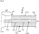
- the Figures 1 and 2 show an electrical connector 1.1, which together with an associated mating connector 1.2 according to FIG Figure 3 a connector arrangement 1 as a B2B connector electrically connects two printed circuit boards, not shown, to one another as shown in FIG.
- a connector arrangement 1 as a B2B connector electrically connects two printed circuit boards, not shown, to one another as shown in FIG.
- the electrical connector 1.1 via a connecting flange 2.10 mechanically and electrically with the one printed circuit board and the mating connector 1.2 via a Connection flange 1.23 mechanically and electrically connected to the other circuit board.
- This connector arrangement 1 has the property that in the event of a lateral offset or angular offset of the connectors 1.1 and 1.2 mechanically connected to the circuit boards with regard to their axes of symmetry, tolerance compensation for this offset is made possible by means of the electrical connector 1.1.
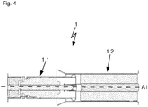
- the connector assembly 1 according to Figure 4 exposed to an angular offset, as can occur, for example, when the circuit boards are not completely aligned parallel to one another, the two connectors 1.1 and 1.2 tilt towards one another. This tilting is compensated for by means of a bending section 2.3 or a bending zone of the electrical connector 2.1 of the connector arrangement 1.
- This compensation or tolerance function of the electrical connector 1.1 which also works with a parallel offset of the circuit boards and thus the axes of symmetry of the connectors 1.1 and 1.2 arranged on them, is explained below.
- the electrical connector 1.1 comprises an outer conductor 2.0 consisting of a sleeve 2a and two inner sleeves 2b, 2c arranged within the sleeve 2a, each extending in the axial direction over a portion of the sleeve 2a, an inner conductor pin 3 as an inner conductor 3.0 and one of the remaining ones Space between the inner conductor 3.0 and the outer conductor 2.0 largely filling the dielectric 4.0, which is constructed as a substantially cylindrical dielectric body 4 in two parts from a first dielectric sub-body 4.1 and a second dielectric sub-body 4.2.
- the sleeve 2a of the electrical connector 1.1 consists of three axial sections, namely an axial holding section 2.1 and an axial compensation section 2.2, which are mechanically connected via the axial bending section 2.3 already mentioned above.
- a connecting flange 2.10 is formed on the free end face of the holding section 2.1, in that the edge area of this end face is widened outward in a funnel shape, thereby creating a contact surface for contact with a printed circuit board and for mechanical connection to the same. Furthermore, this connecting flange 2.10 is provided with radial slots 2.11.
- the compensation section 2.2 ends in a contact zone 2.20 for electrical contacting of the outer conductor 2.0 or the inner conductor 3.0 with an outer conductor 1.210 or an inner conductor 1.240 of the mating connector 1.2 (cf. Figure 4 ).
- an inner sleeve 2c is arranged in the plug-side end area as a further component of the outer conductor 2.0, which is held between the plug-in end area 4.24 of the second dielectric part body 4.2 and the inside of a section of the compensating section 2.2 of the sleeve 2a and is essentially the same up to its plug-side end extends radial distance from the central axis of the electrical connector 1.1.
- circumferential lines L1 and L2 which are adjacent in the axial direction run.
- the axial coordinate of all points on a given circumferential line is always identical; the circumferential lines L1 and L2 are therefore each in a plane, not shown, on which the axial direction is perpendicular.
- Two slots 5.1 and 5.2 are arranged on the circumferential line L1, between each of which there are unslotted areas on the circumferential line L1 and each form a ring segment-like connecting web 5.0.
- the slots 6.1 and 6.2 lying on the circumferential line L2 are arranged offset from one another with respect to the slots 5.1 and 5.2 lying on the circumferential line L1, so that the connecting webs 5.0 and 6.0 are not axially aligned with one another.
- the distance a between the two circumferential lines L1 and L2 is small compared to the axial length L of the electrical connector 1.1.
- the slots 5.1, 5.2, 6.1 and 6.2 have a width b, which can be 1 mm, for example.
- the axial length of the connecting webs 5.0 and 6.0 therefore correspond to the width b of the slots 5.1, 5.2, 6.1 and 6.2.
- the adjacent position of the two circumferential lines L1 and L2 leads to the formation of an annular area 7 between slots 5.1 and 5.2 on the circumferential line L1 and the slots 6.1 and 6.2 on the circumferential line L2.
- the two sections of the sleeve 2, the holding section 2.1 and the compensating section 2.2 are connected via this annular area 7 and on the one hand via the connecting webs 5.0 and on the other hand via the connecting webs 6.0.
- an inner sleeve 2b which is arranged inside the sleeve 2a, is provided as a further component of the outer conductor 2.0.
- the inner sleeve 2b which is elastic, has a holding section 2.5 arranged in the holding section 2.1 of the sleeve 2a, which is in electrical contact with the inner surface of the holding section 2.1 of the sleeve 2a and is preferably attached to this inner surface and / or to the first dielectric sub-body 4.1.
- the inner sleeve 2b has a radially recessed section 2.6, which adjoins the retaining section 2.5 in the plug-in direction and overlaps the bending section 2.3 of the sleeve 2a from the inside, and a connecting section 2.7, which adjoins the radially recessed section 2.6 and is located inside the compensating section 2.2 of the sleeve 2a runs.
- the connecting section 2.7 runs as it is shown in FIG Figure 2 is shown by way of example, preferably at a small distance, which can be, for example, approximately 1 mm or even less than 1 mm, from the second dielectric body 4.2.
- the electrical contact to the compensation section 2.2 of the sleeve 2a is made by a contact section 2.71 of the connecting section 2.7, which protrudes in the radial direction, so that an electrical contact is made to the inside of the compensation section 2.2 of the sleeve 2a, which is particularly good when at least the Connection section 2.7 of the inner sleeve 2a is mechanically preloaded in such a way that the contact section 2.71 is pressed against the inside of the compensating section 2.2 of the sleeve 2a.
- the contact section 2.71 is not firmly connected to the inside of the compensating section 2.2 of the sleeve 2a, so that the contact point or the contact line can shift.
- the elastic bending property must also be ensured for the dielectric 4.0 and the inner conductor 3.0.
- the corresponding flexural elasticity for the dielectric 4.0 is achieved in that the dielectric body 4 is made in two parts from a first partial dielectric body 4.1 arranged in the holding section 2.1 and a second partial dielectric body 4.2 arranged in the compensation section 2.2.
- These two partial dielectric bodies 4.1 and 4.2 are arranged spaced apart in the sleeve 2 by means of a gap 4.3 formed by adjacent end faces 4.11 and 4.21, the gap 4.3, starting from the peripheral surface of the two partial dielectric bodies 4.1 and 4.2, being aligned with the annular region 7 of the bending section 2.3.
- the two end faces 4.11 and 4.21 of the two dielectric part bodies 4.1 and 4.2 are designed with contours that are adapted to one another.
- the end face 4.11 of the first partial dielectric body 4.1 protrudes into the bending section 2.3.
- the first dielectric body 4.1 has a section 4.13, in which its extension in the radial direction is reduced by a step 4.14, around the radially receding one Section 2.6 of the inner sleeve 2b and be able to support it in the axial direction.
- the first dielectric body 4.1 has a central blind hole 4.12, to which the end face 4.21 is adapted with a cylindrical extension 4.22 which dips into the blind hole 4.12.
- the diameter of the extension 4.22 is smaller than the diameter of the blind hole 4.12, so that the gap 4.3, starting from the peripheral surface of the two dielectric sub-bodies 4.1 and 4.2, continues over a radial distance between the extension 4.22 and the peripheral surface of the blind hole 4.12 like a labyrinth to the inner conductor 3.0 .
- the diameter of the second partial dielectric body 4.2 expands in steps, starting from the extension 4.22, via a first step 4.25 and a second step 4.26 up to the full inside diameter of the sleeve 2a.
- the first step 4.25 of the second partial dielectric body 4.2 is designed in terms of its diameter and its axial extent so that it does not come into contact with the recessed section 2.6 of the inner sleeve 2b even with maximum deformation of the bending section 2.3 of the sleeve 2a.
- the second step 4.26 of the second partial dielectric body 4.2 is designed so that it does not come into contact with the contact section 2.71 of the inner sleeve 2b in the axial direction when the bending section 2.3 of the sleeve 2a is maximally deformed.
- the inner conductor 3.0 as the inner conductor pin 3 is mounted in an inner bore 4.10 of the holding section 2.1 and an inner bore 4.20 of the compensating section 2.2, the inner conductor pin 3 having an inner conductor pin 3 in the area of the groove bottom of the blind hole 4.12 on the end face 4.11 of the holding section 2.1 Has cross-sectional tapering 3.1 in the form of a circumferential groove 3.10 with a rectangular cross-section, this groove 3.10 extending into the extension 4.22.
- the inner conductor pin 3 has a diameter d which is slightly smaller than the diameter D of the blind hole 4.20 of the second dielectric part body 4.2.
- Mating connector 1.2 used is in Figure 3 and comprises a sleeve 1.21 as the outer conductor 1.210, in which an inner conductor pin 1.24 is arranged as the inner conductor 1.240 and a cylindrical dielectric body 1.26 is arranged as the dielectric 1.260.
- the mating connector 1.2 has at one end a contact zone 1.22 into which the sleeve 1.21 extends, the plug-side end 1.211 of the sleeve 1.21 expanding outward in a funnel-shaped manner.
- the sleeve 1.21 becomes a connecting flange 1.23, in which the edge area of the sleeve 1.21 is funnel-shaped, forming a contact surface for contact with the circuit board 11 and for the mechanical connection is expanded with the same. Furthermore, this connecting flange 1.23 is provided with radial slots 1.230.
- the dielectric body 1.26 with an inner bore 1.27 for receiving the inner conductor pin 1.24 is located between this connecting flange 1.23 and the contact zone 1.22.
- This inner conductor pin 1.24 has at its end protruding into the contact zone 1.22 a slotted and funnel-shaped widened blind hole 1.25 for receiving the inner conductor pin 3 of the electrical connector 1.1.
- the electrical connector 1.1 according to the Figures 1 and 2 can also be designed with more than two slots 5.1 and 5.2 on a circumferential line L1.
- the electrical connector 1.1 instead of two circumferential lines L1 and L2 provided adjacently in the axial direction, it is also possible to provide only one circumferential line L1 or more than two circumferential lines.
- the plug connection between the electrical connector 1.1 and the mating connector 1.2 takes place according to Figure 4 via the contact zone 2.20 of the connector 1.1, which is designed as a plug, and the contact zone 1.22, which is designed as a socket, of the mating connector 1.2.
- the contact zone 2.20 of the compensating section 2.2 of the sleeve 2 of the mating connector 1.1 has a circumferential and outwardly pointing bead 2.21 with which the end face of the compensating section 2.2 is widened.
- axially extending slots 2.22 are provided in this contact zone 2.20.
- the second partial dielectric body 4.2 ends in front of this contact zone 2.20, the inner conductor pin 3 protruding into this contact zone 2.20.
- the contact section 1.22 of the mating connector 1.2 is pushed onto the connector formed by the contact zone 2.20 of the sleeve 2, so that the groove base of the bead 2.21 on the circumferential surface of the contact zone 1.22 of the sleeve 1.21 forming a Electrical contact is applied and at the same time the end of the inner conductor pin 3 of the electrical connector 1.1 is inserted into the blind hole 1.25 of the inner conductor pin 1.24 of the mating connector 1.2 to form an electrical contact, as shown in FIG Figure 4 can be seen.
Landscapes
- Coupling Device And Connection With Printed Circuit (AREA)
Claims (18)
- Connecteur électrique enfichable (1.1) comprenant :- un conducteur extérieur (2.0) ayant un manchon (2a),- un conducteur intérieur (3.0), et- un diélectrique (4.0) formé par un corps diélectrique cylindrique (4) ayant un perçage intérieur pour recevoir le conducteur intérieur (3.0), dans lequel :- le manchon (2a) est formé d'un segment de maintien axial (2.1) et d'un segment de compensation axial (2.2) reliés par un segment axial de flexion (2.3),- le segment de flexion (2.3) comporte au moins une fente (5.1) qui s'étend sur une ligne périphérique (L1) du manchon (2a),* la zone non fendue formant une entretoise de liaison (5.0) reliant le segment de maintien (2.1) et le segment de compensation (2.2), et- le corps diélectrique (4) a une première partie de corps diélectrique (4.1) logée dans le segment de maintien (2.1) et une seconde partie de corps diélectrique (4.2) logée dans le segment de compensation (2.2),* la première et la seconde parties de corps diélectrique (4.1, 4.2) étant logées de manière écartée l'un de l'autre dans le manchon (2a), connecteur caractérisé en ce que
le conducteur extérieur (2.0) comporte au moins un manchon intérieur (2b, 2c) logé dans le manchon (2a) et s'étendant dans la direction axiale sur une fraction du manchon (2a), et
* le manchon intérieur (2b) s'étend sur le segment de flexion (2.3). - Connecteur électrique enfichable (1.1) selon la revendication 1,
caractérisé en ce que
le manchon intérieur (2b) revient radialement dans le segment de flexion (2.3). - Connecteur électrique enfichable (1.1) selon l'une des revendications 1 ou 2,
caractérisé en ce que
le manchon intérieur (2b) relié au segment de maintien (2.1) par une liaison mécanique solide et une liaison électro-conductrice est en contact électro-conducteur avec le segment extérieur (2.2) pour que le point de contact ou la surface de contact entre le manchon intérieur (2b) et le segment de maintien (2.1) puisse glisser sur la surface intérieure du segment de liaison (2.2). - Connecteur électrique enfichable (1.1) selon l'une des revendications 1 à 3,
caractérisé en ce que
le manchon intérieur (2b) est appuyé contre la première partie de corps diélectrique (4.1) logée dans le segment de maintien (2.1) et/ou est relié à la première partie de corps diélectrique (4.1) logée dans le segment de maintien (2.1). - Connecteur électrique enfichable (1.1) selon l'une des revendications 1 à 4,
caractérisé en ce que
le manchon intérieur (2b) est écarté radialement de la seconde partie de corps diélectrique (4.2) logée dans le segment de compensation (2.2). - Connecteur électrique enfichable (1.1) selon l'une des revendications précédentes,
caractérisé en ce que
le manchon intérieur est mécaniquement précontraint pour exercer une pression sur la surface intérieure du segment de compensation (2.2) au point de contact avec la surface de contact entre le manchon intérieur (2b) et le segment de compensation (2.2). - Connecteur électrique enfichable (1.1) selon l'une des revendications précédentes,
caractérisé en ce que
il comprend un second manchon (2b) s'étendant jusque dans une zone de contact (2.20) du segment de compensation (2.2). - Connecteur électrique enfichable (1.1) selon la revendication 7,
caractérisé en ce que
la zone de contact (2.20) du segment de compensation (2.2) s'élargit en forme d'entonnoir. - Connecteur électrique enfichable (1.1) selon l'une des revendications précédentes,
caractérisé en ce que
le manchon intérieur (2a, 2b) est déformable élastiquement. - Connecteur électrique enfichable (1.1) selon l'une des revendications précédentes,
caractérisé par
au moins deux fentes (5.1, 5.2) l'une derrière l'autre sur la ligne périphérique (L1) du manchon (2a). - Connecteur électrique enfichable (1.1) selon la revendication 1, caractérisé en ce que
le segment de flexion (2.3) comporte au moins deux fentes (5.1, 6.1) dans la direction axiale et décalées l'une par rapport à l'autre. - Connecteur électrique enfichable (1.1) selon l'une des revendications précédentes,
caractérisé en ce que
l'entretoise de liaison (5.0) a une longueur axiale correspondant à la largeur de la fente (5.1). - Connecteur électrique enfichable (1.1) selon l'une des revendications précédentes,
caractérisé en ce que
le conducteur intérieur (3.0) présente une réduction de section (3.1) dans la zone transitoire entre la première partie de corps diélectrique (4.1) et la seconde partie de corps diélectrique (4.2). - Connecteur électrique enfichable (1.1) selon l'une des revendications précédentes,
caractérisé en ce que
dans la zone de la seconde partie de corps diélectrique (4.2), le diamètre du conducteur intérieur (3.0) a un diamètre réduit par comparaison au diamètre du perçage intérieur (4.20) de la seconde partie de corps diélectrique (4.2). - Connecteur électrique enfichable (1.1) selon l'une des revendications précédentes,
caractérisé en ce que
l'une des surfaces frontales (4.11) voisine de la première et de la seconde partie de corps diélectrique (4.1, 4.2) a un perçage borgne (4.12) et l'autre face frontale (4.21) a un contour (4.22) adapté toutefois de diamètre inférieur à celui du perçage borgne (4.12). - Connecteur électrique enfichable (1.1) selon la revendication 7 ou 8,
caractérisé en ce que
la seconde partie de corps diélectrique (4.2) est au-delà de la zone de contact (2.20) dans le segment de compensation (2.2) axial. - Dispositif de connecteur électrique (1) comprenant un connecteur électrique enfichable (1.1) selon l'une des revendications précédentes, et un connecteur complémentaire (1.2),
dispositif caractérisé en ce que
le connecteur complémentaire (1.2) comprend :- un conducteur extérieur (1.210) réalisé comme manchon (1.21) ayant une zone de contact (1.22) pour mettre en contact le conducteur extérieur (2.0) du connecteur enfichable (1.1) et une bride de liaison (2.23) pour réaliser la liaison mécanique électrique avec une plaque de circuit (11),- un conducteur intérieur (1.240) avec un perçage borgne (1.25) pour recevoir le conducteur intérieur (3.0) du connecteur électrique (1.1), et- un diélectrique (1.260) réalisé sous la forme d'un corps diélectrique cylindrique (1.26) ayant un perçage intérieur (1.27) pour recevoir le conducteur intérieur (1.240). - Utilisation du dispositif de connecteur électrique selon la revendication 17, pour réaliser la liaison électrique de deux plaques de circuit.
Applications Claiming Priority (1)
| Application Number | Priority Date | Filing Date | Title |
|---|---|---|---|
| DE102018113278.6A DE102018113278B3 (de) | 2018-06-05 | 2018-06-05 | Elektrischer Steckverbinder für Leiterplatten |
Publications (2)
| Publication Number | Publication Date |
|---|---|
| EP3579346A1 EP3579346A1 (fr) | 2019-12-11 |
| EP3579346B1 true EP3579346B1 (fr) | 2021-08-11 |
Family
ID=66676436
Family Applications (1)
| Application Number | Title | Priority Date | Filing Date |
|---|---|---|---|
| EP19177389.4A Active EP3579346B1 (fr) | 2018-06-05 | 2019-05-29 | Connecteur enfichable électrique pour cartes de circuits imprimés |
Country Status (4)
| Country | Link |
|---|---|
| US (1) | US20190372248A1 (fr) |
| EP (1) | EP3579346B1 (fr) |
| CN (1) | CN110571551B (fr) |
| DE (1) | DE102018113278B3 (fr) |
Families Citing this family (3)
| Publication number | Priority date | Publication date | Assignee | Title |
|---|---|---|---|---|
| DE102020114114B4 (de) | 2020-05-26 | 2022-03-31 | Ims Connector Systems Gmbh | Leiterplatte mit einem Steckverbinderanschluss sowie elektrische Steckverbinderanordnung mit einer solchen Leiterplatte |
| EP3989368A1 (fr) * | 2020-10-20 | 2022-04-27 | Rosenberger Hochfrequenztechnik GmbH & Co. KG | Connecteur enfichable électrique, élément de connecteur et agencement de carte de circuit imprimé |
| CN115316780B (zh) * | 2021-07-21 | 2024-01-12 | 珠海大拇指创新科技有限公司 | 一种折叠式防误触的牙刷 |
Family Cites Families (9)
| Publication number | Priority date | Publication date | Assignee | Title |
|---|---|---|---|---|
| US5516303A (en) * | 1995-01-11 | 1996-05-14 | The Whitaker Corporation | Floating panel-mounted coaxial connector for use with stripline circuit boards |
| JP2001326037A (ja) * | 2000-05-16 | 2001-11-22 | Tokai Rika Co Ltd | プリント配線板用コネクタ装置 |
| DE10202637C1 (de) * | 2002-01-24 | 2003-08-14 | Ims Connector Systems Gmbh | Steckverbinder |
| DE202011108052U1 (de) | 2011-11-18 | 2011-12-06 | Rosenberger Hochfrequenztechnik Gmbh & Co. Kg | Verbindungselement |
| KR101301772B1 (ko) * | 2012-03-06 | 2013-08-29 | 주식회사 텔콘 | 기판 연결용 알에프 커넥터 |
| DK2680372T3 (en) * | 2012-06-29 | 2017-09-11 | Corning Optical Comm Rf Llc | Multiple section insulator for coaxial connector |
| US9484650B2 (en) * | 2012-09-12 | 2016-11-01 | Hypertronics Corporation | Self-adjusting coaxial contact |
| CN203277701U (zh) * | 2013-05-17 | 2013-11-06 | 深圳市天科乐通讯科技有限公司 | Pcb板连接器 |
| DE202015007010U1 (de) * | 2015-10-07 | 2015-10-22 | Rosenberger Hochfrequenztechnik Gmbh & Co. Kg | Verbinder |
-
2018
- 2018-06-05 DE DE102018113278.6A patent/DE102018113278B3/de not_active Expired - Fee Related
-
2019
- 2019-05-29 EP EP19177389.4A patent/EP3579346B1/fr active Active
- 2019-06-05 CN CN201910487175.2A patent/CN110571551B/zh active Active
- 2019-06-05 US US16/432,271 patent/US20190372248A1/en not_active Abandoned
Also Published As
| Publication number | Publication date |
|---|---|
| DE102018113278B3 (de) | 2019-09-12 |
| US20190372248A1 (en) | 2019-12-05 |
| CN110571551A (zh) | 2019-12-13 |
| CN110571551B (zh) | 2021-06-04 |
| EP3579346A1 (fr) | 2019-12-11 |
Similar Documents
| Publication | Publication Date | Title |
|---|---|---|
| EP3227970B1 (fr) | Douille de contact pour connecteur électrique enfichable | |
| EP2529451B1 (fr) | Connecteur coaxial pour circuit intégré | |
| EP3420612B1 (fr) | Connecteur électrique enfichable | |
| EP3251174B1 (fr) | Ensemble connecteur avec sertissage de compensation | |
| EP3103163B1 (fr) | Ensemble connecteur coaxial | |
| EP0856918B1 (fr) | Douille de connection coaxiale | |
| EP3579346B1 (fr) | Connecteur enfichable électrique pour cartes de circuits imprimés | |
| EP2830165A1 (fr) | Agencement de connecteur à fiche coaxial | |
| EP3396791B1 (fr) | Agencement de conducteurs de phase | |
| DE102017112025B4 (de) | Elektrischer Steckverbinder mit Toleranzausgleich | |
| DE102016006598A1 (de) | Steckverbinder | |
| DE102015003935B3 (de) | Verbinder, Verfahren und Verwendung | |
| EP3091613A2 (fr) | Dispositif de raccordement pour un conducteur hf, en particulier pour un cable coaxial et procede de fabrication dudit dispositif de raccordement | |
| EP0583700A1 (fr) | Manchon de sertissage | |
| DE10140153B4 (de) | Steckverbindung zum gleichzeitigen Verbinden mehrerer Koaxialkabel | |
| EP3482465B1 (fr) | Élément de contact à conducteur interne, sollicité par un ressort | |
| EP4010949B1 (fr) | Connecteur électrique mâle | |
| EP3627636A1 (fr) | Connecteur enfichable électrique, raccord de modules et ensemble de carte de circuits imprimés | |
| EP3917294B1 (fr) | Carte de circuit imprimé doté d'un port de connecteur enfichable, ainsi que agencement de connecteur enfichable électrique doté d'une telle carte de circuit imprimé | |
| EP3605746B1 (fr) | Connecteur enfichable ainsi que connexion enfichable doté d'un tel connecteur enfichable | |
| DE102016006923B4 (de) | Koaxialsteckverbinder | |
| EP3482461B1 (fr) | Dispositif de contact électrique | |
| DE202004015503U1 (de) | Steckanordnung für HF-Signalweg | |
| DE102015106058B4 (de) | Steckverbindersystem | |
| EP4092835B1 (fr) | Connecteur enfichable électrique, agencement de connecteur enfichable électrique et connecteur enfichable électrique |
Legal Events
| Date | Code | Title | Description |
|---|---|---|---|
| PUAI | Public reference made under article 153(3) epc to a published international application that has entered the european phase |
Free format text: ORIGINAL CODE: 0009012 |
|
| STAA | Information on the status of an ep patent application or granted ep patent |
Free format text: STATUS: THE APPLICATION HAS BEEN PUBLISHED |
|
| AK | Designated contracting states |
Kind code of ref document: A1 Designated state(s): AL AT BE BG CH CY CZ DE DK EE ES FI FR GB GR HR HU IE IS IT LI LT LU LV MC MK MT NL NO PL PT RO RS SE SI SK SM TR |
|
| AX | Request for extension of the european patent |
Extension state: BA ME |
|
| STAA | Information on the status of an ep patent application or granted ep patent |
Free format text: STATUS: REQUEST FOR EXAMINATION WAS MADE |
|
| 17P | Request for examination filed |
Effective date: 20200512 |
|
| RBV | Designated contracting states (corrected) |
Designated state(s): AL AT BE BG CH CY CZ DE DK EE ES FI FR GB GR HR HU IE IS IT LI LT LU LV MC MK MT NL NO PL PT RO RS SE SI SK SM TR |
|
| GRAP | Despatch of communication of intention to grant a patent |
Free format text: ORIGINAL CODE: EPIDOSNIGR1 |
|
| STAA | Information on the status of an ep patent application or granted ep patent |
Free format text: STATUS: GRANT OF PATENT IS INTENDED |
|
| INTG | Intention to grant announced |
Effective date: 20210323 |
|
| GRAS | Grant fee paid |
Free format text: ORIGINAL CODE: EPIDOSNIGR3 |
|
| GRAA | (expected) grant |
Free format text: ORIGINAL CODE: 0009210 |
|
| STAA | Information on the status of an ep patent application or granted ep patent |
Free format text: STATUS: THE PATENT HAS BEEN GRANTED |
|
| AK | Designated contracting states |
Kind code of ref document: B1 Designated state(s): AL AT BE BG CH CY CZ DE DK EE ES FI FR GB GR HR HU IE IS IT LI LT LU LV MC MK MT NL NO PL PT RO RS SE SI SK SM TR |
|
| REG | Reference to a national code |
Ref country code: CH Ref legal event code: EP |
|
| REG | Reference to a national code |
Ref country code: DE Ref legal event code: R096 Ref document number: 502019002000 Country of ref document: DE |
|
| REG | Reference to a national code |
Ref country code: IE Ref legal event code: FG4D Free format text: LANGUAGE OF EP DOCUMENT: GERMAN Ref country code: AT Ref legal event code: REF Ref document number: 1420349 Country of ref document: AT Kind code of ref document: T Effective date: 20210915 |
|
| REG | Reference to a national code |
Ref country code: LT Ref legal event code: MG9D |
|
| REG | Reference to a national code |
Ref country code: NL Ref legal event code: MP Effective date: 20210811 |
|
| PG25 | Lapsed in a contracting state [announced via postgrant information from national office to epo] |
Ref country code: HR Free format text: LAPSE BECAUSE OF FAILURE TO SUBMIT A TRANSLATION OF THE DESCRIPTION OR TO PAY THE FEE WITHIN THE PRESCRIBED TIME-LIMIT Effective date: 20210811 Ref country code: NO Free format text: LAPSE BECAUSE OF FAILURE TO SUBMIT A TRANSLATION OF THE DESCRIPTION OR TO PAY THE FEE WITHIN THE PRESCRIBED TIME-LIMIT Effective date: 20211111 Ref country code: PT Free format text: LAPSE BECAUSE OF FAILURE TO SUBMIT A TRANSLATION OF THE DESCRIPTION OR TO PAY THE FEE WITHIN THE PRESCRIBED TIME-LIMIT Effective date: 20211213 Ref country code: LT Free format text: LAPSE BECAUSE OF FAILURE TO SUBMIT A TRANSLATION OF THE DESCRIPTION OR TO PAY THE FEE WITHIN THE PRESCRIBED TIME-LIMIT Effective date: 20210811 Ref country code: BG Free format text: LAPSE BECAUSE OF FAILURE TO SUBMIT A TRANSLATION OF THE DESCRIPTION OR TO PAY THE FEE WITHIN THE PRESCRIBED TIME-LIMIT Effective date: 20211111 Ref country code: RS Free format text: LAPSE BECAUSE OF FAILURE TO SUBMIT A TRANSLATION OF THE DESCRIPTION OR TO PAY THE FEE WITHIN THE PRESCRIBED TIME-LIMIT Effective date: 20210811 Ref country code: SE Free format text: LAPSE BECAUSE OF FAILURE TO SUBMIT A TRANSLATION OF THE DESCRIPTION OR TO PAY THE FEE WITHIN THE PRESCRIBED TIME-LIMIT Effective date: 20210811 Ref country code: ES Free format text: LAPSE BECAUSE OF FAILURE TO SUBMIT A TRANSLATION OF THE DESCRIPTION OR TO PAY THE FEE WITHIN THE PRESCRIBED TIME-LIMIT Effective date: 20210811 Ref country code: FI Free format text: LAPSE BECAUSE OF FAILURE TO SUBMIT A TRANSLATION OF THE DESCRIPTION OR TO PAY THE FEE WITHIN THE PRESCRIBED TIME-LIMIT Effective date: 20210811 |
|
| PG25 | Lapsed in a contracting state [announced via postgrant information from national office to epo] |
Ref country code: PL Free format text: LAPSE BECAUSE OF FAILURE TO SUBMIT A TRANSLATION OF THE DESCRIPTION OR TO PAY THE FEE WITHIN THE PRESCRIBED TIME-LIMIT Effective date: 20210811 Ref country code: LV Free format text: LAPSE BECAUSE OF FAILURE TO SUBMIT A TRANSLATION OF THE DESCRIPTION OR TO PAY THE FEE WITHIN THE PRESCRIBED TIME-LIMIT Effective date: 20210811 Ref country code: GR Free format text: LAPSE BECAUSE OF FAILURE TO SUBMIT A TRANSLATION OF THE DESCRIPTION OR TO PAY THE FEE WITHIN THE PRESCRIBED TIME-LIMIT Effective date: 20211112 |
|
| PG25 | Lapsed in a contracting state [announced via postgrant information from national office to epo] |
Ref country code: NL Free format text: LAPSE BECAUSE OF FAILURE TO SUBMIT A TRANSLATION OF THE DESCRIPTION OR TO PAY THE FEE WITHIN THE PRESCRIBED TIME-LIMIT Effective date: 20210811 |
|
| PG25 | Lapsed in a contracting state [announced via postgrant information from national office to epo] |
Ref country code: DK Free format text: LAPSE BECAUSE OF FAILURE TO SUBMIT A TRANSLATION OF THE DESCRIPTION OR TO PAY THE FEE WITHIN THE PRESCRIBED TIME-LIMIT Effective date: 20210811 |
|
| REG | Reference to a national code |
Ref country code: DE Ref legal event code: R097 Ref document number: 502019002000 Country of ref document: DE |
|
| PG25 | Lapsed in a contracting state [announced via postgrant information from national office to epo] |
Ref country code: SM Free format text: LAPSE BECAUSE OF FAILURE TO SUBMIT A TRANSLATION OF THE DESCRIPTION OR TO PAY THE FEE WITHIN THE PRESCRIBED TIME-LIMIT Effective date: 20210811 Ref country code: SK Free format text: LAPSE BECAUSE OF FAILURE TO SUBMIT A TRANSLATION OF THE DESCRIPTION OR TO PAY THE FEE WITHIN THE PRESCRIBED TIME-LIMIT Effective date: 20210811 Ref country code: RO Free format text: LAPSE BECAUSE OF FAILURE TO SUBMIT A TRANSLATION OF THE DESCRIPTION OR TO PAY THE FEE WITHIN THE PRESCRIBED TIME-LIMIT Effective date: 20210811 Ref country code: EE Free format text: LAPSE BECAUSE OF FAILURE TO SUBMIT A TRANSLATION OF THE DESCRIPTION OR TO PAY THE FEE WITHIN THE PRESCRIBED TIME-LIMIT Effective date: 20210811 Ref country code: CZ Free format text: LAPSE BECAUSE OF FAILURE TO SUBMIT A TRANSLATION OF THE DESCRIPTION OR TO PAY THE FEE WITHIN THE PRESCRIBED TIME-LIMIT Effective date: 20210811 Ref country code: AL Free format text: LAPSE BECAUSE OF FAILURE TO SUBMIT A TRANSLATION OF THE DESCRIPTION OR TO PAY THE FEE WITHIN THE PRESCRIBED TIME-LIMIT Effective date: 20210811 |
|
| PLBE | No opposition filed within time limit |
Free format text: ORIGINAL CODE: 0009261 |
|
| STAA | Information on the status of an ep patent application or granted ep patent |
Free format text: STATUS: NO OPPOSITION FILED WITHIN TIME LIMIT |
|
| 26N | No opposition filed |
Effective date: 20220512 |
|
| PG25 | Lapsed in a contracting state [announced via postgrant information from national office to epo] |
Ref country code: IT Free format text: LAPSE BECAUSE OF FAILURE TO SUBMIT A TRANSLATION OF THE DESCRIPTION OR TO PAY THE FEE WITHIN THE PRESCRIBED TIME-LIMIT Effective date: 20210811 |
|
| PG25 | Lapsed in a contracting state [announced via postgrant information from national office to epo] |
Ref country code: SI Free format text: LAPSE BECAUSE OF FAILURE TO SUBMIT A TRANSLATION OF THE DESCRIPTION OR TO PAY THE FEE WITHIN THE PRESCRIBED TIME-LIMIT Effective date: 20210811 |
|
| REG | Reference to a national code |
Ref country code: CH Ref legal event code: PL |
|
| REG | Reference to a national code |
Ref country code: BE Ref legal event code: MM Effective date: 20220531 |
|
| PG25 | Lapsed in a contracting state [announced via postgrant information from national office to epo] |
Ref country code: MC Free format text: LAPSE BECAUSE OF FAILURE TO SUBMIT A TRANSLATION OF THE DESCRIPTION OR TO PAY THE FEE WITHIN THE PRESCRIBED TIME-LIMIT Effective date: 20210811 Ref country code: LU Free format text: LAPSE BECAUSE OF NON-PAYMENT OF DUE FEES Effective date: 20220529 Ref country code: LI Free format text: LAPSE BECAUSE OF NON-PAYMENT OF DUE FEES Effective date: 20220531 Ref country code: CH Free format text: LAPSE BECAUSE OF NON-PAYMENT OF DUE FEES Effective date: 20220531 |
|
| PG25 | Lapsed in a contracting state [announced via postgrant information from national office to epo] |
Ref country code: IE Free format text: LAPSE BECAUSE OF NON-PAYMENT OF DUE FEES Effective date: 20220529 |
|
| PG25 | Lapsed in a contracting state [announced via postgrant information from national office to epo] |
Ref country code: BE Free format text: LAPSE BECAUSE OF NON-PAYMENT OF DUE FEES Effective date: 20220531 |
|
| PGFP | Annual fee paid to national office [announced via postgrant information from national office to epo] |
Ref country code: FR Payment date: 20230517 Year of fee payment: 5 Ref country code: DE Payment date: 20230626 Year of fee payment: 5 |
|
| GBPC | Gb: european patent ceased through non-payment of renewal fee |
Effective date: 20230529 |
|
| PG25 | Lapsed in a contracting state [announced via postgrant information from national office to epo] |
Ref country code: MK Free format text: LAPSE BECAUSE OF FAILURE TO SUBMIT A TRANSLATION OF THE DESCRIPTION OR TO PAY THE FEE WITHIN THE PRESCRIBED TIME-LIMIT Effective date: 20210811 Ref country code: CY Free format text: LAPSE BECAUSE OF FAILURE TO SUBMIT A TRANSLATION OF THE DESCRIPTION OR TO PAY THE FEE WITHIN THE PRESCRIBED TIME-LIMIT Effective date: 20210811 Ref country code: GB Free format text: LAPSE BECAUSE OF NON-PAYMENT OF DUE FEES Effective date: 20230529 |