EP3578875A1 - Method of mounting and adjusting a dmd chip in a light module for a motor vehicle headlamp - Google Patents
Method of mounting and adjusting a dmd chip in a light module for a motor vehicle headlamp Download PDFInfo
- Publication number
- EP3578875A1 EP3578875A1 EP19177675.6A EP19177675A EP3578875A1 EP 3578875 A1 EP3578875 A1 EP 3578875A1 EP 19177675 A EP19177675 A EP 19177675A EP 3578875 A1 EP3578875 A1 EP 3578875A1
- Authority
- EP
- European Patent Office
- Prior art keywords
- dmd chip
- circuit board
- dmd
- carrier element
- module
- Prior art date
- Legal status (The legal status is an assumption and is not a legal conclusion. Google has not performed a legal analysis and makes no representation as to the accuracy of the status listed.)
- Granted
Links
- 238000000034 method Methods 0.000 title claims abstract description 20
- 239000000853 adhesive Substances 0.000 claims description 21
- 230000001070 adhesive effect Effects 0.000 claims description 21
- 238000003825 pressing Methods 0.000 claims description 5
- 230000005489 elastic deformation Effects 0.000 claims description 3
- 230000002787 reinforcement Effects 0.000 claims description 3
- 238000009826 distribution Methods 0.000 description 5
- 239000006096 absorbing agent Substances 0.000 description 4
- 230000000295 complement effect Effects 0.000 description 2
- 238000011156 evaluation Methods 0.000 description 2
- 239000004065 semiconductor Substances 0.000 description 2
- ONNCPBRWFSKDMQ-UHFFFAOYSA-N 2,3',5-trichlorobiphenyl Chemical compound ClC1=CC=CC(C=2C(=CC=C(Cl)C=2)Cl)=C1 ONNCPBRWFSKDMQ-UHFFFAOYSA-N 0.000 description 1
- 241001295925 Gegenes Species 0.000 description 1
- 230000003321 amplification Effects 0.000 description 1
- 230000015572 biosynthetic process Effects 0.000 description 1
- 150000001875 compounds Chemical class 0.000 description 1
- 230000001419 dependent effect Effects 0.000 description 1
- 230000000694 effects Effects 0.000 description 1
- 239000011521 glass Substances 0.000 description 1
- 238000003384 imaging method Methods 0.000 description 1
- 239000002655 kraft paper Substances 0.000 description 1
- 230000001795 light effect Effects 0.000 description 1
- 239000011159 matrix material Substances 0.000 description 1
- 238000003199 nucleic acid amplification method Methods 0.000 description 1
- 230000003287 optical effect Effects 0.000 description 1
- 229920003023 plastic Polymers 0.000 description 1
- 230000000644 propagated effect Effects 0.000 description 1
- 230000005855 radiation Effects 0.000 description 1
- IHQKEDIOMGYHEB-UHFFFAOYSA-M sodium dimethylarsinate Chemical class [Na+].C[As](C)([O-])=O IHQKEDIOMGYHEB-UHFFFAOYSA-M 0.000 description 1
Images


Classifications
-
- F—MECHANICAL ENGINEERING; LIGHTING; HEATING; WEAPONS; BLASTING
- F21—LIGHTING
- F21S—NON-PORTABLE LIGHTING DEVICES; SYSTEMS THEREOF; VEHICLE LIGHTING DEVICES SPECIALLY ADAPTED FOR VEHICLE EXTERIORS
- F21S41/00—Illuminating devices specially adapted for vehicle exteriors, e.g. headlamps
- F21S41/60—Illuminating devices specially adapted for vehicle exteriors, e.g. headlamps characterised by a variable light distribution
- F21S41/67—Illuminating devices specially adapted for vehicle exteriors, e.g. headlamps characterised by a variable light distribution by acting on reflectors
- F21S41/675—Illuminating devices specially adapted for vehicle exteriors, e.g. headlamps characterised by a variable light distribution by acting on reflectors by moving reflectors
-
- F—MECHANICAL ENGINEERING; LIGHTING; HEATING; WEAPONS; BLASTING
- F21—LIGHTING
- F21S—NON-PORTABLE LIGHTING DEVICES; SYSTEMS THEREOF; VEHICLE LIGHTING DEVICES SPECIALLY ADAPTED FOR VEHICLE EXTERIORS
- F21S41/00—Illuminating devices specially adapted for vehicle exteriors, e.g. headlamps
- F21S41/30—Illuminating devices specially adapted for vehicle exteriors, e.g. headlamps characterised by reflectors
- F21S41/39—Attachment thereof
Definitions
- the present application relates to a method for mounting a DMD chip-carrying printed circuit board in a DMD (Digital Mirror Device) light module for a motor vehicle headlight.
- a DMD Digital Mirror Device
- Such a light module is from the DE 198 22 142 C2 known.
- the light module emits a light beam having a main emission direction.
- the radiation takes place in a lying in front of the motor vehicle headlight area so that it is illuminated.
- a front side refers to a side facing this room area.
- a back side is in each case a side facing away from this room area.
- the known light module has a printed circuit board, the has a front and a back and carries on its front a DMD chip.
- the DMD chip has a micromirror-bearing front side and a rear side opposite its front side.
- the known light module furthermore has a central carrier element which has a front side and a rear side.
- Available DMD chips can have a large number (greater than one million) of micromirrors.
- Each individual micromirror is, for example, only 8 by 8 microns in size.
- One position of each individual micromirror can be switched between two positions. In one position, it reflects incident light from a light source via a primary optic to a secondary optic of the light module, and in the other position reflects the light, for example, onto an absorber.
- the secondary optics form the arrangement of the micromirrors in the apron of the light module, which is in the case of a motor vehicle headlight, for example, on the roadway from.
- Micro mirrors that reflect light onto the secondary optics appear as bright pixels in the light distribution resulting from the image, whereas the micromirrors that reflect light onto the absorber appear as dark pixels in the light distribution.
- the shape of the light distribution with a predetermined by the number of pixels and thus by the number of micromirrors fineness is controllable, which allows, for example, camera-controlled light distributions in which areas that would dazzle other road users, can be specifically darkened and Other areas, such as traffic signs or pedestrians, are specifically illuminated so that they are recognized by the driver.
- a common method for mounting a DMD chip-carrying circuit board in a light module of a motor vehicle headlight provides an adjustment of the mounting position of the chip with a pin slot structure.
- chip and board have mutually complementary form-fitting elements such as pins and, holes and slots.
- This type of alignment of a DMD chip on a printed circuit board of a light module is not accurate enough for use in automotive headlamps. It may, for example, cause the motor vehicle headlight to produce undesired tilted light distributions. For example, it may happen that an oblique light-dark boundary is generated instead of a light-dark boundary parallel to the horizon.
- the object of the invention is to provide an improved method of the type mentioned.
- the clamping force acting in this case lies in a defined by the deformation of the elastic element Anpresskraft Scotland Symposium.
- the contact pressure in the assembled state is preferably between 40 N and 80 N.
- a preferred embodiment is characterized in that the pressing force is generated by an elastic connecting element of the clamping element assembly as a restoring force of an elastic deformation, which experiences the elastic connecting element during assembly of the light module.
- the image processing takes place in such a way that the position and the course of at least one outer edge of the reflecting surface of the arrangement of the micromirrors are determined
- fixation is effected by adhesive bonds.
- a further preferred embodiment is characterized in that the printed circuit board is glued floating in the aligned state with the central carrier element.
- circuit board 26 arranged recesses, which are opposite receptacles of the central support member, filled with a viscous adhesive, wherein the adhesive also penetrates between the edges of the recesses and the receptacles.
- the adhesive bonds 36 be irradiated with ultraviolet light for a period between 15 seconds and 30 seconds.
- a further preferred embodiment is characterized in that the adhesive bonds are cured end-time after the irradiation with ultraviolet light at elevated temperature.
- fixation is complementarily by an increase in the contact pressure with which the DMD chip is held clamped.
- the reinforcement of the clamping force takes place by tightening screws with which the clamping element assembly is fastened to screw domes of the central carrier element.
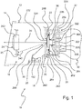
- FIG. 1 shows in detail a sectional view of a motor vehicle headlight 10 with a housing 12, the light exit opening is covered by a transparent cover 14.
- the cutting plane is at a proper use of the motor vehicle headlight 10 in a motor vehicle parallel to a plane which is spanned by a longitudinal axis and a vertical axis of the motor vehicle.
- a light module 16 In the interior of the housing 12, a light module 16 is arranged.
- the light module 16 has, among other things Light source 18, a primary optics 20, a DMD chip 22, a secondary optics 24 and an absorber 25 on.
- the light module 16 furthermore has a printed circuit board 26, a central carrier element 28 and a clamping element assembly 30.
- the clamping element assembly 30 has a punch 302 and an elastic connecting element 32.
- the tensioner assembly may also include a heat sink 304.
- the printed circuit board 26, together with the central carrier element 28, the DMD chip 22 and the clamping element assembly 30 forms a partial module of the light module.
- the printed circuit board 26 has a front side 260, a back side 262 and a printed circuit board window 264 and carries on its front side 260 the DMD chip 22.
- the DMD chip 22 has a micromirror 222-bearing front side 224 and a rear side 226 opposite its front side 226.
- the central carrier element 28 has a front side 282, a rear side 284 and a carrier element window 286.
- the printed circuit board 26 is arranged with its front side 260 facing the rear side 284 of the central carrier element 28 such that the front side 224 of the DMD chip 22 covers the carrier element window 286, wherein the micromirrors 222 are arranged in the opening of the carrier element window 286.
- An opening of the circuit board window 264 is completely or partially covered by the rear side 226 of the DMD chip 22.
- the clamping element assembly 30 has a punch 302, which is supported by the PCB window 264 on the back 226 of the DMD chip 22. Incidentally, that is, with the heat sink 304 of the clamping element assembly 30, which is not projecting through the printed circuit board window 264 between the printed circuit board 26 and the central support element 28, the clamping element assembly 30 is disposed on the back 262 of the printed circuit board 26.
- the elastic connecting element 32 has at least one clamping element assembly-side end 322 and at least one carrier element-side end 324.
- the elastic connecting element 32 With its clamping element assembly side end 322, the elastic connecting element 32 is rigidly connected to the arranged on the back 262 of the circuit board 26 remaining part of the clamping element assembly 30 having, for example, a heat sink 304.
- the elastic connecting element 32 With its carrier element-side end 324, the elastic connecting element 32 is rigidly connected to the central support element 28.
- the light source 18 is a semiconductor light source 182 which is arranged on a circuit board 35 and which emits light 34 in the direction of the primary optics 20.
- the primary optic 20 directs the light 34 incident from the semiconductor light source 182 onto the micromirrors 222 arranged on the front side 224 of the DMD chip 22. How and with which optical elements of the primary optics 20 this is done in detail is not essential to the invention. In the case of FIG. 1 the primary optics 20 is a concave mirror reflector.
- a pivotal position of the micromirrors 222 is individual for each micromirror or at least for different groups (subsets) of the micromirrors 222 between a first pivotal position and a second pivotal position switchable.
- Each micromirror which is in the first pivot position, deflects the light 34 incident on it from the primary optics 20 to the secondary optics 24.
- Each micromirror which is located in the second pivot position, deflects the light 34 incident on it from the primary optics 20 so that this light 342 does not fall on the secondary optics 24. For example, this light 342 is directed to the absorber 25 and absorbed there, so that it can not produce any disturbing light effects.
- the secondary optics 24 directs the light 34 incident on them from the DMD chip 22 into the apron of the light module 16. When the light module 16 is used as intended, this light 34 illuminates the road ahead of the motor vehicle.
- the secondary optics 24 has a secondary optic lens 242 of transparent plastic or glass.
- the secondary optics 24 may also have a plurality of lenses, for example an arrangement of an achromatic lens and an imaging lens.
- the DMD chip 22 has two broad sides in the form of the front side 224 and the rear side 226, the front side 224 and the rear side 226 being separated from one another by lateral narrow sides 228 lying between them.
- the front side 224 of the DMD chip 22 has a central chip area, in which the micromirrors 222 are arranged, and has a flange area 229, which circumscribes the central chip area in a closed curve, in which no micromirrors 222 are arranged.
- the number of micromirrors is about 1.3 million, arranged in a matrix of 1152 columns and 1152 rows.
- FIG. 2 also shows that the DMD chip 22 is disposed in a socket 266 of the circuit board 26 and held.
- the mechanical support of the DMD chip 22 in the base 266 via the lateral narrow sides 228 and possibly additionally on parts of the back 226 of the DMD chip 22, and the electrical contacting is also via the lateral narrow sides 228 and / or on the Rear side 226 of the DMD chip 22 from the circuit board 26 from.
- the printed circuit board 26 is fixedly connected to the central support element 28.
- the compound is preferably carried out in the FIG. 1 illustrated adhesive connections 36.
- the circuit board 26 exerts no perpendicular to the surface of the circuit board 26 and the front side 224 of the DMD chip 22 acting contact force. However, the circuit board 26 holds the DMD chip 22 with its socket 266 in tangential to the front side 224 of the DMD chip 22 and the circuit board 26 lying directions.
- Said pressing force is generated by the elastic member 32 as a restoring force of elastic deformation which the elastic connecting member 32 undergoes during assembly of the light module 16.
- This contact force is transmitted from the punch 302 to the back of the DMD chip 22 and presses the flange portion 229 of the DMD chip 22 against the back of the central support member 28th
- a leaf spring 326 serving as an elastic connecting element 32 is rigidly connected with its carrier element-side end 324 to the central carrier element 28.
- the central support element 28 has screw domes 289, which protrude from the back 284 of the central support member 28. On their ends remote from the rear side 284, the screw domes 289 have receptacles for the carrier element-side ends 324 of the leaf spring 326.
- the leaf spring 326 With its clamping element assembly-side end 322, the leaf spring 326 is non-positively and / or positively connected to the lying on the back 262 of the circuit board 26 remaining part of the clamping element assembly 30, which may be a heat sink 304. In the FIG. 1 this connection is made by interlocking elements 306 of the clamping element assembly 30, which prevent the clamping element assembly-side end 322 of the leaf spring 326 from moving toward the printed circuit board 26.
- the elastic connecting element 32 is first deformed to a first extent, in which it generates the certain contact force.
- the pressing force is adjusted so that the circuit board 26 is initially floating relative to the receptacles 288 of the central support member 28 in the circuit board plane.
- the circuit board 26 according to the invention with the aid of a camera and image processing-based alignment device together with the fixed in the base 266 of the PCB 26 DMD chip 22 aligned so that the directions in which the micromirrors 222 from the primary optics 20 ago reflect incident light 34 corresponds to the desired desired directions.
- the circuit board 26 is glued with the adhesive bonds 36 with the receptacles 288 of the central support member 28 stress-free. Only then are the screw, with which the leaf spring 326 with the screw domes 289th is screwed, finally tightened.
- the elastic connecting member 32 is deformed in total to a second extent, which is larger than the first extent. Therefore, the restoring force and thus the contact pressure at endfest tightened screws is greater than before.
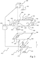
- FIG. 3 shows an appropriate for carrying out a method according to the invention alignment device 400.
- the evaluation device 400 has a continuous and rigid frame 402, which forms a reference frame for the alignment of the circuit board with the DMD chip.
- the central support element 28 is in the alignment by accurately produced positive or negative positive locking elements 404 such as corners, edges or pins or recesses of the central support member 28, which in each case negatively or positively complementary positive locking elements 404 'of the rigid framework or one with the rigid framework dimensionally accurate engage associated tool carrier, held in a precisely defined within the frame reference position and location. This is in the FIG. 3 by representing the pair of lines connecting the central support member 28 to the rigid framework 402.
- the central carrier element 28 is inserted directly into a correspondingly precise and accurately manufactured part of the framework 402.
- the central support member 28 is received by a portable tool carrier, with which the central support member 28 and mounted thereon further components of the light module are transported from processing station to processing station.
- a tool carrier is with respect to its inclusion by the framework 402 and in With respect to its receptacle for the central support element manufactured so dimensionally accurate that the central support member 28 is held in this embodiment in a precisely predetermined position and position within the reference frame.
- position refers to a translational coordinate in said reference frame.
- posture refers to a rotational angle in said reference frame.
- the alignment device 400 has a camera 406.
- the camera 406 captures images of the DMD chip 22 in the board plane or a plane parallel thereto, and simultaneously captures images of fiducial marks 405 of the tool carrier and / or the central support member 28.
- fiducial 405 may be, for example, an edge of the support member window 286 .
- the camera 406 is preferably arranged to face the front side 282 of the central support member 28 and to receive images of the front side 224 of the DMD chip 22 through the support member window 286.
- FIG. 3 also shows that the printed circuit board 26 has recesses 268, and that the central support element 28 has receptacles 288 in the form of flat regions at its locations adjacent to the recesses 268 of the printed circuit board 26. These flat areas project beyond the recesses 268 parallel to the planes in which the recesses 268 lie.
- the recesses 268 preferably have a clear width, which is between 5 mm and 10 mm. Between the edges of the recesses 268 and the receptacles 288 in the assembled state is preferably a narrow gap whose thickness is preferably smaller or equal to 1 mm.
- the receptacles 288 therefore preferably do not touch the edges of the recesses 268. These structures serve to produce the adhesive bonds 36 (cf. Figure. 1 ).
- the alignment device 400 has a control unit 408, which is set up, in particular programmed to evaluate the images captured by the camera 406 with the aid of an image processing program.
- the evaluation is preferably carried out such that the position and the course of at least one outer edge 225 of the reflecting surface of the arrangement of the micromirrors 222 (cf. FIG. 2 ).
- the controller 408 thus determines quantitative values for the position and angle of rotation of the DMD chip 22 in the reference system.
- the alignment device 400 has a gripper 410.
- a base of the gripper 410 is rigidly connected to at least one actuator 412, with which the gripper 410 is movable parallel to an xy plane of the reference system of the alignment device 400 and with which it is rotatable about a rotation axis parallel to the z-direction and with the Opening and closing the gripper 410, ie the gripping is driven.
- the actuator 412 is controlled by the controller 408 in response to the position information and / or rotational angle information that the controller generates from the signals of the camera 406.
- FIG. 4 shows a flowchart as an embodiment of a method according to the invention for mounting a DMD chip 22-bearing circuit board 26 in a DMD light module 16 for a motor vehicle headlight 10.
- a partial module of the light module 16 having the printed circuit board 26, a central carrier element 28 and a clamping element assembly 30, as shown in FIG FIG. 1 is shown prepared.
- the central carrier element 28 of this sub-module has a carrier element window 286 and is elastically connected to the clamping element assembly 30.
- the DMD chip 22 between a frame of the carrier element window 286 and the clamping element assembly 30 is frictionally clamped and thereby held movable in a plane parallel to the circuit board plane against the resistance of a force resulting from the clamping force frictional force.
- a reference system for the position and position of the DMD chip 22 relative to the central support element 28 is determined.
- the setting is made by inserting the sub-module in an alignment device 400, as described with reference to the FIG. 3 and comprising a gripper 410 movably controllable by an actuator 412, a video signal generating camera 406, and an image signal of the camera 406 to control signals to the actuator 412 processing control unit 408
- a third step 504 the circuit board 26 is gripped with the gripper 410 of the alignment device 400.
- the position and position of the circuit board 26 with the DMD chip 22 are the controller 408 then known.
- a fourth step 506 at least one image of at least one position feature and / or at least one position feature of the DMD chip 22 is recorded in the alignment device 400 through the carrier element window 286 therethrough.
- a fifth step 508 the position and position of the DMD chip 22 are calculated in the reference system of the alignment device 400 in response to signals from the camera 406 and a formation of drive signals with which the controller 408 controls the gripper 410 in a sixth step.
- the control signals are each formed so that the gripper 410 sets the desired position and desired position of the circuit board 26 with the DMD chip 22 by the circuit board 26 is rotated by the gripper 410 and moved in translation accordingly.
- the control of the position of the gripper 410 in response to a deviation of the position and position of the DMD chip 26 from a desired position and desired position takes place in a sixth step 510 such that the DMD chip (26) the desired position and desired position occupies.
- the clamping support of the DMD chip 22 between its abutment against the frame of the carrier element window 286 and the punch 302 of the clamping element assembly 30 allows these movements and sets them only one by the drive of the gripper 410 overcome frictional resistance.
- a seventh step 512 the position and location of the DMD chip 22 in the central support member 28 is further propagated, i. over the already existing clamping bracket out, fixed when the target position and target position is reached.
- this is done both by adhesive bonds 36 as well as by an amplification of the clamping force with which the DMD chip 22 is clamped.
- the adhesive bonds 36 are the Recesses 268 filled with a viscous adhesive, the adhesive may preferably between the edges of the recesses 268 and the receptacles 288 may penetrate.
- the adhesive is preferably of a variety that cures rapidly upon exposure to ultraviolet light.
- the adhesive bonds 36 are preferably irradiated with ultraviolet light for a period between 15 seconds and 30 seconds.
- the circuit board 26 is glued floating in the aligned state with the central support member 28.
- the printed circuit board 26 does not have to transmit any forces acting perpendicular to the printed circuit board plane. As a result, for example, an undesired swinging up of the printed circuit board 26 during subsequent operation is effectively avoided, which advantageously improves the reliability and the durability of the light module 16 during later operation of the light module 16 in the motor vehicle headlight 10.
- the reinforcement of the clamping force is carried out by endfestes tightening the screws with which the clamping element assembly 30 is attached to the screw domes 289 of the central support member 28.
Abstract
Vorgestellt wird eine Verfahren zum Montieren einer einen DMD Chip tragenden Leiterplatte in einem DMD-Lichtmodul für einen Kraftfahrzeugscheinwerfer. Das Verfahren zeichnet sich durch folgende Schritte aus: Herstellen eines Teilmoduls des Lichtmoduls, wobei das zentrale Trägerelement elastisch mit der Spannelementbaugruppe verbunden ist und wobei der DMD-Chip zwischen dem Trägerelement und dem Spannelement klemmend gehalten wird, Festlegen eines Bezugssystems durch Einlegen des Teilmoduls in eine Ausrichtevorrichtung, die einen durch ein Stellglied beweglich steuerbaren Greifer, eine bildsignalerzeugende Kamera, und ein Bildsignale der Kamera zu Stellsignalen für das Stellglied verarbeitendes Steuergerät aufweist, Steuern der Position des Greifers in Abhängigkeit von einer Abweichung der Lage und Position des DMD-Chips von einer Soll-Lage und Sollposition so, dass der DMD-Chip die Sollposition und Soll-Lage einnimmt, und Fixieren des DMD-Chips in dem zentralen Trägerelement, wenn die Sollposition und Soll-Lage erreicht ist.A method is presented for mounting a circuit board carrying a DMD chip in a DMD light module for a motor vehicle headlight. The method is characterized by the following steps: production of a sub-module of the light module, wherein the central support element is elastically connected to the clamping element assembly and wherein the DMD chip is held clamped between the support element and the clamping element, establishing a reference system by inserting the sub-module into a Alignment device, which has a gripper movably controllable by an actuator, a camera generating image signals, and a control device that processes image signals from the camera to control signals for the actuator, controlling the position of the gripper as a function of a deviation of the location and position of the DMD chip from a target -Location and target position so that the DMD chip assumes the target position and target position, and fixing the DMD chip in the central support element when the target position and target position is reached.
Description
Die vorliegende Anmeldung betrifft ein Verfahren zum Montieren einer einen DMD-Chip tragenden Leiterplatte in einem DMD-Lichtmodul (DMD: Digital Mirror Device) für einen Kraftfahrzeugscheinwerfer. Ein solches Lichtmodul ist aus der
Das Lichtmodul strahlt ein eine Hauptabstrahlrichtung aufweisendes Lichtbündel ab. Bei einer bestimmungsgemäßen Verwendung erfolgt die Abstrahlung in einen vor dem Kraftfahrzeugscheinwerfer liegenden Raumbereich, so dass dieser beleuchtet wird. Wenn in der vorliegenden Anmeldung eine Vorderseite erwähnt wird, ist damit jeweils eine Seite gemeint, die diesem Raumbereich zugewandt ist. Eine Rückseite ist jeweils eine diesem Raumbereich abgewandte Seite.The light module emits a light beam having a main emission direction. When used as intended, the radiation takes place in a lying in front of the motor vehicle headlight area so that it is illuminated. When a front side is mentioned in the present application, it refers to a side facing this room area. A back side is in each case a side facing away from this room area.
Das bekannte Lichtmodul weist eine Leiterplatte auf, die eine Vorderseite und eine Rückseite aufweist und die auf ihrer Vorderseite einen DMD-Chip trägt. Der DMD-Chip weist eine Mikrospiegel tragende Vorderseite und eine seiner Vorderseite gegenüberliegende Rückseite auf. Das bekannte Lichtmodul weist darüber hinaus ein zentrales Trägerelement auf, das eine Vorderseite und eine Rückseite aufweist.The known light module has a printed circuit board, the has a front and a back and carries on its front a DMD chip. The DMD chip has a micromirror-bearing front side and a rear side opposite its front side. The known light module furthermore has a central carrier element which has a front side and a rear side.
Zur Verfügung stehende DMD-Chips können eine große Zahl (größer als eine Million) von Mikrospiegeln aufweisen. Jeder einzelne Mikrospiegel ist dabei zum Beispiel nur 8 mal 8 Mikrometer groß. Eine Stellung jedes einzelnen Mikrospiegels ist zwischen zwei Stellungen umschaltbar. In einer Stellung reflektiert er von einer Lichtquelle über eine Primäroptik einfallendes Licht auf eine Sekundäroptik des Lichtmoduls, und in der anderen Stellung reflektiert er das Licht zum Beispiel auf einen Absorber. Die Sekundäroptik bildet die Anordnung der Mikrospiegel in das Vorfeld des Lichtmoduls, das bei einem Kraftfahrzeugscheinwerfer zum Beispiel auf der Fahrbahn liegt, ab.Available DMD chips can have a large number (greater than one million) of micromirrors. Each individual micromirror is, for example, only 8 by 8 microns in size. One position of each individual micromirror can be switched between two positions. In one position, it reflects incident light from a light source via a primary optic to a secondary optic of the light module, and in the other position reflects the light, for example, onto an absorber. The secondary optics form the arrangement of the micromirrors in the apron of the light module, which is in the case of a motor vehicle headlight, for example, on the roadway from.
Mikrospiegel, die Licht auf die Sekundäroptik spiegeln, erscheinen in der aus der Abbildung resultierenden Lichtverteilung als helle Pixel, während die Mikrospiegel, die Licht auf den Absorber spiegeln, in der Lichtverteilung als dunkle Pixel erscheinen. Im Ergebnis ist damit die Form der Lichtverteilung mit einer durch die Zahl der Pixel und damit durch die Zahl der Mikrospiegel vorgegebenen Feinheit steuerbar, was zum Beispiel Kamera-gesteuerte Lichtverteilungen ermöglicht, bei denen Bereiche, die andere Verkehrsteilnehmer blenden würden, gezielt abgedunkelt werden können und andere Bereiche, zum Beispiel Verkehrsschilder oder Fußgänger, gezielt beleuchtet werden, damit sie vom Fahrer erkannt werden.Micro mirrors that reflect light onto the secondary optics appear as bright pixels in the light distribution resulting from the image, whereas the micromirrors that reflect light onto the absorber appear as dark pixels in the light distribution. As a result, the shape of the light distribution with a predetermined by the number of pixels and thus by the number of micromirrors fineness is controllable, which allows, for example, camera-controlled light distributions in which areas that would dazzle other road users, can be specifically darkened and Other areas, such as traffic signs or pedestrians, are specifically illuminated so that they are recognized by the driver.
Ein übliches Verfahren zum Montieren einer einen DMD-Chip tragenden Leiterplatte in einem Lichtmodul eines Kraftfahrzeugscheinwerfers sieht eine Justierung der Einbaulage des Chips mit einer Pin-Langloch Struktur vor. Dabei weisen Chip und Platine zueinander komplementäre Formschlusselemente wie Pins und, Löcher und Langlöcher auf. Diese Art der Ausrichtung eines DMD-Chips auf einer Leiterplatte eines Lichtmoduls ist für die Verwendung in Kraftfahrzeugscheinwerfern nicht genau genug. Sie kann zum Beispiel dazu führen, dass der Kraftfahrzeugscheinwerfer unerwünscht verkippte Lichtverteilungen erzeugt. So kann es zum Beispiel dazu kommen, dass an Stelle einer parallel zum Horizont liegenden Hell-Dunkel-Grenze eine schräg liegende Hell-Dunkel-Grenze erzeugt wird.A common method for mounting a DMD chip-carrying circuit board in a light module of a motor vehicle headlight provides an adjustment of the mounting position of the chip with a pin slot structure. In this case, chip and board have mutually complementary form-fitting elements such as pins and, holes and slots. This type of alignment of a DMD chip on a printed circuit board of a light module is not accurate enough for use in automotive headlamps. It may, for example, cause the motor vehicle headlight to produce undesired tilted light distributions. For example, it may happen that an oblique light-dark boundary is generated instead of a light-dark boundary parallel to the horizon.
Die Aufgabe der Erfindung besteht in der Angabe eines verbesserten Verfahrens der eingangs genannten Art.The object of the invention is to provide an improved method of the type mentioned.
Diese Aufgabe wird mit den Merkmalen des Anspruchs 1 gelöst. Dessen kennzeichnende Merkmale sehen die folgenden Schritte vor:
- Herstellen eines die Leiterplatte, ein zentrales Trägerelement und eine Spannelementbaugruppe aufweisenden Teilmoduls des Lichtmoduls, wobei das zentrale Trägerelement ein Trägerelementfenster aufweist und elastisch mit der Spannelementbaugruppe verbunden ist und wobei der DMD-Chip zwischen einem Rahmen des Trägerelementfensters und dem Spannelement kraftschlüssig klemmend und dabei in einer zur Leiterplattenebene parallelen Ebene gegen den Widerstand einer aus der klemmenden Kraft resultierenden Reibungskraft beweglich gehalten wird,
- Festlegen eines Bezugssystems für die Lage und Position des DMD-Chips relativ zum zentralen Trägerelement durch Einlegen des Teilmoduls in eine Ausrichtevorrichtung, die einen durch ein Stellglied beweglich steuerbaren Greifer, eine bildsignalerzeugende Kamera, und ein Bildsignale der Kamera zu Stellsignalen für das Stellglied verarbeitendes Steuergerät aufweist,
- Greifen der Leiterplatte mit dem Greifer,
- Aufnehmen von wenigstens einem Bild von wenigstens einem Lagemerkmal und/oder wenigstens einem Positionsmerkmal des DMD-Chips in der Ausrichtevorrichtung durch das Trägerelementfenster hindurch,
- Berechnen der Lage und Position des DMD-Chips in dem Bezugssystem der Ausrichtevorrichtung in Abhängigkeit von Signalen der Kamera,
- Steuern der Position des Greifers in Abhängigkeit von einer Abweichung der Lage und Position des DMD-Chips von einer Soll-Lage und Sollposition so, dass der DMD-Chip die Sollposition und Soll-Lage einnimmt, und
- Fixieren des DMD-Chips in dem zentralen Trägerelement, wenn die Sollposition und Soll-Lage erreicht ist.
- Producing a the circuit board, a central support member and a clamping element assembly having submodule of the light module, wherein the central support member has a support element window and is elastically connected to the clamping element assembly and wherein the DMD chip between a frame of the support member window and the clamping element force-locking and thereby in a plane parallel to the circuit board plane is kept movable against the resistance of a frictional force resulting from the clamping force,
- Set a reference system for the location and Position of the DMD chip relative to the central support element by inserting the sub-module in an alignment device, which has a controllable by an actuator gripper, a video signal generating camera, and an image signals from the camera to control signals for the actuator processing control unit,
- Gripping the circuit board with the gripper,
- Picking up at least one image of at least one position feature and / or at least one position feature of the DMD chip in the alignment device through the carrier element window,
- Calculating the position and position of the DMD chip in the reference frame of the alignment device in response to signals from the camera,
- Controlling the position of the gripper in response to a deviation of the position and position of the DMD chip from a desired position and target position so that the DMD chip assumes the desired position and target position, and
- Fixing the DMD chip in the central support element when the desired position and target position is reached.
Durch diese Merkmale wird die Leiterplatte zusammen mit dem DMD-Chip ausgerichtet. Dadurch wird die Summe der Toleranzen der Lagen und Positionen von DMD-Chip auf der Leiterplatte und der Leiterplatte in Bezug zu dem zentralen Trägerelement kompensiert. Wenn man die Leiterplattenebene als x-y-Ebene eines rechtshändig-rechtwinkligen Koordinatensystems mit x-, y- und z-Koordinaten betrachtet, dann wird der DMD-Chip in der z-Richtung klemmend gehalten, ohne dass die Leiterplatte in dieser Richtung irgendwelche Haltekräfte übertragen muss. Dadurch muss sie insbesondere im späteren, Vibrationen ausgesetzten Betrieb auch keine Massenkräfte übertragen. Dadurch wird ein Aufschwingen der Leiterplatte in dieser Schwingungsrichtung wirksam vermieden. In den innerhalb der Leiterplattenebene liegenden Richtungen wirkende Kräfte können, soweit sie nicht Haftreibungskräfte der klemmenden Halterungen übersteigen, durch die Leiterplatte aufgefangen werden, da die Leiterplatte in diesen Richtungen sehr steif ist.These features align the PCB with the DMD chip. This compensates for the sum of the tolerances of the locations and positions of the DMD chip on the circuit board and the circuit board relative to the central support element. Considering the circuit board plane as the xy plane of a right-right orthogonal coordinate system with x, y, and z coordinates, the DMD chip is clamped in the z direction without the circuit board having to transmit any holding forces in that direction , As a result, it does not have to, especially in the later, vibration-exposed operation Transmit mass forces. As a result, a swinging of the circuit board in this direction of vibration is effectively avoided. In the directions lying within the board plane, forces can be absorbed by the board unless they exceed the frictional forces of the clamping mounts because the board is very stiff in these directions.
Die klemmend wirkende Anpresskraft liegt dabei in einem durch die Verformung des elastischen Elements definierten Anpresskraftbereich. Dadurch können Auswirkungen von Lagetoleranzen des DMD-Chips auf die auf ihn einwirkende Anpresskraft kompensiert werden. Im Bereich üblicher Toleranzen verändert sich die Verformung des elastischen Elements und damit die von ihm erzeugte Anpresskraft nur wenig. Die Anpresskraft wird durch das elastische Element auf dessen Rückstellkräfte beschränkt, was Beschädigungen durch zu hohe Anpresskräfte, wie sie bei anderen Befestigungen, zum Beispiel bei weniger elastischen Verschraubungen, auftreten können, sicher verhindert. Die Anpresskraft liegt im fertig montierten Zustand bevorzugt zwischen 40 N und 80 N.The clamping force acting in this case lies in a defined by the deformation of the elastic element Anpresskraftbereich. As a result, the effects of position tolerances of the DMD chip on the contact force acting on it can be compensated. In the range of usual tolerances, the deformation of the elastic element and thus the contact pressure generated by it changes only slightly. The contact pressure is limited by the elastic element on the restoring forces, which safely prevents damage due to excessive contact forces, as they can occur in other fasteners, for example, in less elastic fittings. The contact pressure in the assembled state is preferably between 40 N and 80 N.
Eine bevorzugte Ausgestaltung zeichnet sich dadurch aus, dass die Anpresskraft von einem elastischen Verbindungselement der Spannelementbaugruppe als Rückstellkraft einer elastischen Verformung erzeugt wird, die das elastische Verbindungselement beim Zusammenbau des Lichtmoduls erfährt.A preferred embodiment is characterized in that the pressing force is generated by an elastic connecting element of the clamping element assembly as a restoring force of an elastic deformation, which experiences the elastic connecting element during assembly of the light module.
Bevorzugt ist auch, dass die Bildverarbeitung so erfolgt, dass die Lage und der Verlauf von wenigstens einer Außenkante der spiegelnden Fläche der Anordnung der Mikrospiegel bestimmt werdenIt is also preferred that the image processing takes place in such a way that the position and the course of at least one outer edge of the reflecting surface of the arrangement of the micromirrors are determined
Weiter ist bevorzugt, dass die Fixierung durch Klebeverbindungen erfolgt.It is further preferred that the fixation is effected by adhesive bonds.
Eine weitere bevorzugte Ausgestaltung zeichnet sich dadurch aus, dass die Leiterplatte im ausgerichteten Zustand mit dem zentralen Trägerelement schwimmend verklebt wird.A further preferred embodiment is characterized in that the printed circuit board is glued floating in the aligned state with the central carrier element.
Bevorzugt ist auch, dass in der Leiterplatte 26 angeordnete Ausnehmungen, denen Aufnahmen des zentralen Trägerelements gegenüberliegen, mit einem zähflüssigen Kleber ausgefüllt werden, wobei der Kleber auch zwischen die Ränder der Ausnehmungen und die Aufnahmen eindringt.It is also preferred that in the
Weiter ist bevorzugt, dass die Klebeverbindungen 36 für eine Zeitdauer zwischen 15 s und 30 s mit ultraviolettem Licht bestrahlt werden.Further, it is preferable that the
Eine weitere bevorzugte Ausgestaltung zeichnet sich dadurch aus, dass die Klebeverbindungen zeitlich nach der Bestrahlung mit ultraviolettem Licht bei erhöhter Temperatur endfest ausgehärtet werden.A further preferred embodiment is characterized in that the adhesive bonds are cured end-time after the irradiation with ultraviolet light at elevated temperature.
Bevorzugt ist auch, dass die Fixierung ergänzend durch eine Verstärkung der Anpresskraft, mit welcher der DMD-Chip klemmend gehalten wird, erfolgt.It is also preferred that the fixation is complementarily by an increase in the contact pressure with which the DMD chip is held clamped.
Weiter ist bevorzugt, dass die Verstärkung der Klemmkraft durch endfestes Anziehen von Schrauben erfolgt, mit denen die Spannelementbaugruppe an Schraubdomen des zentralen Trägerelements befestigt ist.It is further preferred that the reinforcement of the clamping force takes place by tightening screws with which the clamping element assembly is fastened to screw domes of the central carrier element.
Weitere Vorteile ergeben sich aus der nachfolgenden Beschreibung, den Zeichnungen und den Unteransprüchen. Es versteht sich, dass die vorstehend genannten und die nachstehend noch zu erläuternden Merkmale nicht nur in der jeweils angegebenen Kombination, sondern auch in anderen Kombinationen oder in Alleinstellung verwendbar sind, ohne den Rahmen der vorliegenden Erfindung zu verlassen.Further advantages will become apparent from the following description, the drawings and the dependent claims. It is understood that the above and the hereinafter to be explained features not only in the particular combination given, but also in other combinations or alone, without departing from the scope of the present invention.
Ausführungsbeispiele der Erfindung sind in den Zeichnungen dargestellt und werden in der nachfolgenden Beschreibung näher erläutert.Embodiments of the invention are illustrated in the drawings and are explained in more detail in the following description.
Dabei zeigen, jeweils in schematischer Form:
- Figur 1
- ein Ausführungsbeispiel eines erfindungsgemäßen Lichtmoduls in einer Schnittansicht;
- Figur 2
- einen DMD-Chip;
- Figur 3
- eine Ausrichtevorrichtung; und
- Figur 4
- ein Flussdiagramm als Ausführungsbeispiel eines erfindungsgemäßen Verfahrens.
- FIG. 1
- an embodiment of a light module according to the invention in a sectional view;
- FIG. 2
- a DMD chip;
- FIG. 3
- an alignment device; and
- FIG. 4
- a flowchart as an embodiment of a method according to the invention.
Die Schnittebene liegt bei einer bestimmungsgemäßen Verwendung des Kraftfahrzeugscheinwerfers 10 in einem Kraftfahrzeug parallel zu einer Ebene, die von einer Längsachse und einer Hochachse des Kraftfahrzeuges aufgespannt wird.The cutting plane is at a proper use of the
Im Innenraum des Gehäuses 12 ist ein Lichtmodul 16 angeordnet. Das Lichtmodul 16 weist unter anderem eine Lichtquelle 18, eine Primäroptik 20, einen DMD-Chip 22, eine Sekundäroptik 24 und einen Absorber 25 auf. Das Lichtmodul 16 weist darüber hinaus eine Leiterplatte 26, ein zentrales Trägerelement 28 und eine Spannelementbaugruppe 30 auf. Die Spannelementbaugruppe 30 weist einen Stempel 302 und ein elastisches Verbindungselement 32 auf. Die Spannelementbaugruppe kann auch einen Kühlkörper 304 aufweisen. Die Leiterplatte 26 bildet zusammen mit dem zentralen Trägerelement 28, dem DMD-Chip 22 und der Spannelementbaugruppe 30 ein Teilmodul des Lichtmoduls.In the interior of the
Die Leiterplatte 26 weist eine Vorderseite 260, eine Rückseite 262 und ein Leiterplattenfenster 264 auf und trägt auf ihrer Vorderseite 260 den DMD-Chip 22. Der DMD-Chip 22 weist eine Mikrospiegel 222 tragende Vorderseite 224 und eine seiner Vorderseite 224 gegenüberliegende Rückseite 226 auf. Das zentrale Trägerelement 28 weist eine Vorderseite 282, eine Rückseite 284 und ein Trägerelementfenster 286 auf.The printed
Die Leiterplatte 26 ist mit ihrer Vorderseite 260 der Rückseite 284 des zentralen Trägerelements 28 zugewandt so angeordnet, dass die Vorderseite 224 des DMD-Chips 22 das Trägerelementfenster 286 abdeckt, wobei die Mikrospiegel 222 in der Öffnung des Trägerelementfensters 286 angeordnet sind. Eine Öffnung des Leiterplattenfensters 264 wird von der Rückseite 226 des DMD-Chips 22 ganz oder zum Teil abgedeckt.The printed
Die Spannelementbaugruppe 30 weist einen Stempel 302 auf, der sich durch das Leiterplattenfenster 264 hindurch an der Rückseite 226 des DMD-Chips 22 abstützt. Im Übrigen, d.h., mit dem Kühlkörper 304 der Spannelementbaugruppe 30, welcher nicht durch das Leiterplattenfenster 264 hindurch ragend zwischen der Leiterplatte 26 und dem zentralen Trägerelement 28 liegt, ist die Spannelementbaugruppe 30 auf der Rückseite 262 der Leiterplatte 26 angeordnet.The clamping
Das elastische Verbindungselement 32 weist wenigstens ein Spannelementbaugruppen-seitiges Ende 322 und wenigstens ein Trägerelement-seitiges Ende 324 auf.The elastic connecting
Mit seinem Spannelementbaugruppen-seitigen Ende 322 ist das elastische Verbindungselement 32 starr mit dem auf der Rückseite 262 der Leiterplatte 26 angeordneten übrigen Teil der Spannelementbaugruppe 30 verbunden, der zum Beispiel einen Kühlkörper 304 aufweist.With its clamping element
Mit seinem Trägerelement-seitigen Ende 324 ist das elastische Verbindungselement 32 starr mit dem zentralen Trägerelement 28 verbunden.With its carrier element-
Die Lichtquelle 18 ist eine Halbleiterlichtquelle 182, die auf einer Platine 35 angeordnet ist und die Licht 34 in Richtung zu der Primäroptik 20 abstrahlt. Die Primäroptik 20 richtet das von der Halbleiterlichtquelle 182 her einfallende Licht 34 auf die Mikrospiegel 222, die auf der Vorderseite 224 des DMD-Chips 22 angeordnet sind. Wie und mit welchen optischen Elementen der Primäroptik 20 dies im Einzelnen geschieht, ist für die Erfindung nicht wesentlich. Im Fall der
Eine Schwenkstellung der Mikrospiegel 222 ist individuell für jeden Mikrospiegel oder zumindest für verschiedene Gruppen (Teilmengen) der Mikrospiegel 222 zwischen einer ersten Schwenkstellung und einer zweiten Schwenkstellung umschaltbar. Jeder Mikrospiegel, der sich in der ersten Schwenkstellung befindet, lenkt das auf ihn von der Primäroptik 20 her einfallende Licht 34 auf die Sekundäroptik 24 um. Jeder Mikrospiegel, der sich in der zweiten Schwenkstellung befindet, lenkt das auf ihn von der Primäroptik 20 her einfallende Licht 34 so ab, dass dieses Licht 342 nicht auf die Sekundäroptik 24 fällt. Dieses Licht 342 wird zum Beispiel auf den Absorber 25 gelenkt und dort absorbiert, so dass es keine störenden Lichteffekte erzeugen kann.A pivotal position of the
Die Sekundäroptik 24 richtet das auf sie von dem DMD-Chip 22 her einfallende Licht 34 in das Vorfeld des Lichtmoduls 16. Bei einer bestimmungsgemäßen Verwendung des Lichtmoduls 16 wird mit diesem Licht 34 die vor dem Kraftfahrzeug liegende Fahrbahn ausgeleuchtet. Die Sekundäroptik 24 weist eine Sekundäroptiklinse 242 aus transparentem Kunststoff oder Glas auf. Die Sekundäroptik 24 kann auch mehrere Linsen aufweisen, zum Beispiel eine Anordnung aus einem Achromaten und einer abbildenden Linse.The
Wie
Dabei übt die Leiterplatte 26 keine senkrecht zur Fläche der Leiterplatte 26 und der Vorderseite 224 des DMD-Chips 22 wirkende Anpresskraft aus. Die Leiterplatte 26 hält den DMD-Chip 22 mit ihrem Sockel 266 jedoch in tangential zur Vorderseite 224 des DMD-Chips 22 und der Leiterplatte 26 liegenden Richtungen fest.In this case, the
Die genannte Anpresskraft wird von dem elastischen Element 32 als Rückstellkraft einer elastischen Verformung erzeugt, die das elastische Verbindungselement 32 beim Zusammenbau des Lichtmoduls 16 erfährt. Diese Anpresskraft wird von dem Stempel 302 auf die Rückseite des DMD-Chips 22 übertragen und drückt den Flanschbereich 229 des DMD-Chips 22 gegen die Rückseite des zentralen Trägerelements 28.Said pressing force is generated by the
Im zusammengebauten Zustand ist eine als elastisches Verbindungselement 32 dienende Blattfeder 326 mit ihrem Trägerelement-seitigen Ende 324 starr mit dem zentralen Trägerelement 28 verbunden. Das zentrale Trägerelement 28 weist Schraubdome 289 auf, die aus der Rückseite 284 des zentralen Trägerelements 28 herausragen. Auf ihren von der Rückseite 284 abgewandten Enden weisen die Schraubdome 289 Aufnahmen für die Trägerelement-seitigen Enden 324 der Blattfeder 326 auf.In the assembled state, a
Mit ihrem Spannelementbaugruppen-seitigen Ende 322 ist die Blattfeder 326 kraftschlüssig und/oder formschlüssig mit dem auf der Rückseite 262 der Leiterplatte 26 liegenden übrigen Teil der Spannelementbaugruppe 30 verbunden, der ein Kühlkörper 304 sein kann. In der
Durch den Stempel 302, mit dem sich die Spannelementbaugruppe 30 durch das Leiterplattenfenster 264 hindurch an der Rückseite 226 des DMD-Chips 22 abstützt, ergibt sich beim Zusammenbau des Lichtmoduls 16 vor einem Herstellen der Schraubverbindungen zunächst ein Abstand zwischen den Blattfeder-seitigen Enden der Schraubdome 289 und den Trägerelement-seitigen Enden 324 der Blattfeder 326 in einer zur Rückseite 262 der Leiterplatte 26 senkrechten Richtung. Beim Herstellen der Schraubverbindung verschwindet dieser Abstand zwischen den Blattfeder-seitigen Enden der Schraubdome 289 und den Trägerelement-seitigen Enden 324 der Blattfeder 326, wobei die Blattfeder 326 elastisch verformt wird. Dabei ergibt sich eine zum DMD-Chip 22 gerichtete Anpresskraft, die von dem Stempel 302 durch das Leiterplattenfenster 264 hindurch auf die Rückseite des 226 des DMD-Chips 22 übertragen wird und die diesen auf den rückseitigen Rand des Trägerelementfensters 286 drückt.By means of the
Bei der Montage des Lichtmoduls 16 erfolgt das Herstellen der Schraubverbindung zwischen den Blattfeder-seitigen Enden der Schraubdome 289 und den Trägerelement-seitigen Enden 324 der Blattfeder 326 bevorzugt in zwei Stufen: In einer ersten Stufe erfolgt die Schraubverbindung nur so weit, dass das elastische Verbindungselement 32 noch nicht seine volle Rückstellkraft erzeugt, wobei die Schraubverbindung aber doch so weit hergestellt wird, dass der DMD-Chip 22 schon mit einer gewissen, wenn auch nicht mit der vollen Anpresskraft auf die Rückseite 284 des zentralen Trägerelements 28 gedrückt wird. Wenn zum endfesten Anziehen der Schraubverbindung zum Beispiel m Umdrehungen erforderlich sind, erfolgen zunächst zum Beispiel nur k < m Umdrehungen, wobei k zum Beispiel = m/2 ist. Das elastische Verbindungselement 32 wird dabei zunächst in einem ersten Ausmaß verformt, in dem es die gewisse Anpresskraft erzeugt.When assembling the
Dabei wird die Anpresskraft so eingestellt, dass die Leiterplatte 26 dabei zunächst relativ zu den Aufnahmen 288 des zentralen Trägerelements 28 in der Leiterplattenebene schwimmend beweglich ist. In diesem Zustand wird die Leiterplatte 26 erfindungsgemäß mit Hilfe einer kamera- und Bildverarbeitungs- gestützten Ausrichtevorrichtung zusammen mit dem im Sockel 266 der Leiterplatte 26 fest sitzenden DMD-Chip 22 so ausgerichtet, dass die Richtungen, in welche die Mikrospiegel 222 von der Primäroptik 20 her einfallendes Licht 34 reflektieren, den gewünschten Sollrichtungen entspricht. Nach erfolgter Ausrichtung wird die Leiterplatte 26 mit den Klebeverbindungen 36 mit den Aufnahmen 288 des zentralen Trägerelements 28 spannungsfrei verklebt. Erst danach werden die Schraubverbindungen, mit denen die Blattfeder 326 mit den Schraubdomen 289 verschraubt wird, endfest angezogen. Dabei wird das elastische Verbindungselement 32 insgesamt in einem zweiten Ausmaß verformt, das größer als das erste Ausmaß ist. Daher ist auch die Rückstellkraft und damit auch die Anpresskraft bei endfest angezogenen Schrauben größer als vorher.In this case, the pressing force is adjusted so that the
Das zentrale Trägerelement 28 wird in der Ausrichtvorrichtung durch maßgenau hergestellte positive oder negative Formschlusselemente 404 wie Ecken, Kanten oder Stifte oder Ausnehmungen des zentralen Trägerelements 28, die in dazu jeweils negativ oder positiv komplementäre Formschlusselemente 404' des starren Gerüstes oder eines mit dem starren Gerüst maßgenau verbundenen Werkzeugträger eingreifen, in einer innerhalb des Bezugssystems präzise vorbestimmten Position und Lage gehalten. Dies wird in der
Das zentrale Trägerelement 28 wird in einer Ausgestaltung direkt in einen entsprechend präzise und maßgenau hergestellten Teil des Gerüstes 402 eingelegt. In einer dazu alternativen Ausgestaltung wird das zentrale Trägerelement 28 durch einen transportablen Werkzeugträger aufgenommen, mit dem das zentrale Trägerelement 28 und daran anmontierte weitere Bestandteile des Lichtmoduls von Bearbeitungsstation zu Bearbeitungsstation weitertransportiert werden. Ein solcher Werkzeugträger ist in Bezug auf seine Aufnahme durch das Gerüst 402 und in Bezug auf seine Aufnahme für das zentrale Trägerelement so maßgenau hergestellt, dass das zentrale Trägerelement 28 auch bei dieser Ausgestaltung in einer innerhalb des Bezugssystems präzise vorbestimmten Position und Lage gehalten wird.In one embodiment, the
Wenn in dieser Anmeldung der Begriff einer Position genannt wird, so bezieht sich dies auf eine translatorische Koordinate in dem genannten Bezugssystem. Wenn dagegen eine Lage genannt wird, bezieht sich dies auf einen Drehwinkel in dem genannten Bezugssystem.When the term "position" is used in this application, this refers to a translational coordinate in said reference frame. On the other hand, when a posture is called, it refers to a rotational angle in said reference frame.
Die Ausrichtevorrichtung 400 weist eine Kamera 406 auf. Die Kamera 406 erfasst Bilder des DMD-Chips 22 in der Leiterplattenebene oder einer dazu parallelen Ebene, und sie erfasst gleichzeitig Bilder von Bezugsmarkierungen 405 des Werkzeugträgers und/oder des zentralen Trägerelements 28. Eine solche Bezugsmarkierung 405 kann zum Beispiel eine Kante des Trägerelementfensters 286 sein. Die Kamera 406 ist bevorzugt so angeordnet, dass sie der Vorderseite 282 des zentralen Trägerelements 28 zugewandt ist und Bilder der Vorderseite 224 des DMD-Chips 22 durch das Trägerelementfenster 286 hindurch aufnimmt.The
Die Ausrichtevorrichtung 400 weist ein Steuergerät 408 auf, das dazu eingerichtet, insbesondere dazu programmiert ist, die von der Kamera 406 erfassten Bilder mit Hilfe eines Bildverarbeitungsprogramms auszuwerten. Die Auswertung erfolgt bevorzugt so, dass die Lage und der Verlauf von wenigstens einer Außenkante 225 der spiegelnden Fläche der Anordnung der Mikrospiegel 222 (vergleiche
Das Steuergerät 408 ermittelt auf diese Weise quantitative Werte für die Position und den Drehwinkel des DMD-Chips 22 in dem Bezugsystem.The
Die Ausrichtevorrichtung 400 weist einen Greifer 410 auf. Eine Basis des Greifers 410 ist starr mit wenigstens einem Stellglied 412 verbunden, mit dem der Greifer 410 parallel zu einer x-y-Ebene des Bezugsystems der Ausrichtevorrichtung 400 bewegbar ist und mit dem er um eine zur z-Richtung parallele Drehachse drehbar ist und mit dem das Öffnen und Schließen des Greifers 410, d.h. das Greifen, angetrieben wird. Das Stellglied 412 wird von dem Steuergerät 408 in Abhängigkeit von den Positionsinformationen und/oder Drehwinkelinformationen gesteuert, die das Steuergerät aus den Signalen der Kamera 406 erzeugt.The
In einem ersten Schritt 500 wird ein die Leiterplatte 26, ein zentrales Trägerelement 28 und eine Spannelementbaugruppe 30 aufweisendes Teilmodul des Lichtmoduls 16, wie es in der
In einem zweiten Schritt 502 wird ein Bezugssystem für die Lage und Position des DMD-Chips 22 relativ zum zentralen Trägerelement 28 festgelegt. Das Festlegen erfolgt durch Einlegen des Teilmoduls in eine Ausrichtevorrichtung 400, wie sie unter Bezug auf die
In einem dritten Schritt 504 wird die Leiterplatte 26 mit dem Greifer 410 der Ausrichtevorrichtung 400 gegriffen. Die Position und Lage der Leiterplatte 26 mit dem DMD-Chip 22 sind dem Steuergerät 408 dann bekannt.In a
In einem vierten Schritt 506 erfolgt ein Aufnehmen von wenigstens einem Bild von wenigstens einem Lagemerkmal und/oder wenigstens einem Positionsmerkmal des DMD-Chips 22 in der Ausrichtevorrichtung 400 durch das Trägerelementfenster 286 hindurch.In a
In einem fünften Schritt 508 erfolgt ein Berechnen der Lage und Position des DMD-Chips 22 in dem Bezugssystem der Ausrichtevorrichtung 400 in Abhängigkeit von Signalen der Kamera 406 und eine Bildung von Ansteuersignalen, mit denen das Steuergerät 408 den Greifer 410 in einem sechsten Schritt steuert. Die Ansteuersignale werden dabei jeweils so gebildet, dass der Greifer 410 die Soll-Lage und SollPosition der Leiterplatte 26 mit dem DMD-Chip 22 einstellt, indem die Leiterplatte 26 durch den Greifer 410 entsprechend gedreht und translatorisch bewegt wird.In a
Das Steuern der Position des Greifers 410 in Abhängigkeit von einer Abweichung der Lage und Position des DMD-Chips 26 von einer Soll-Lage und Sollposition erfolgt in einem sechsten Schritt 510 so, dass der DMD-Chip (26) die Sollposition und Soll-Lage einnimmt. Die klemmende Halterung des DMD-Chips 22 zwischen seiner Anlage an dem Rahmen des Trägerelementfensters 286 und dem Stempel 302 der Spannelementbaugruppe 30 erlaubt diese Bewegungen und setzt ihnen nur einen durch den Antrieb des Greifers 410 überwindbaren Reibungswiderstand entgegen.The control of the position of the
In einem siebten Schritt 512 wird die Position und Lage des DMD-Chips 22 in dem zentralen Trägerelement 28 weiter, d.h. über die bereits vorhandene klemmende Halterung hinaus, fixiert, wenn die Sollposition und Soll-Lage erreicht ist.In a
In einer bevorzugten Ausgestaltung erfolgt dies sowohl durch Klebeverbindungen 36 als auch durch eine Verstärkung der Klemmkraft, mit welcher der DMD-Chip 22 klemmend gehalten wird.In a preferred embodiment, this is done both by
Zum Herstellen der Klebeverbindungen 36 werden die Ausnehmungen 268 mit einem zähflüssigen Kleber ausgefüllt, wobei der Kleber bevorzugt auch zwischen die Ränder der Ausnehmungen 268 und die Aufnahmen 288 eindringen darf. Der Kleber ist bevorzugt von einer Sorte, die bei einer Bestrahlung mit ultraviolettem Licht rasch aushärtet. Um eine solche rasche Aushärtung zu erzielen, werden die Klebeverbindungen 36 bevorzugt für eine Zeitdauer zwischen 15 s und 30 s mit ultraviolettem Licht bestrahlt. Auf diese Weise wird die Leiterplatte 26 im ausgerichteten Zustand mit dem zentralen Trägerelement 28 schwimmend verklebt. Die Leiterplatte 26 muss im Folgenden keine senkrecht zur Leiterplattenebene wirkenden Kräfte übertragen. Dadurch wird zum Beispiel ein unerwünschtes Aufschwingen der Leiterplatte 26 im späteren Betrieb wirksam vermieden, was die Zuverlässigkeit und die Dauerhaltbarkeit des Lichtmoduls 16 im späteren Betrieb des Lichtmoduls 16 in dem Kraftfahrzeugscheinwerfer 10 vorteilhaft verbessert.To produce the
Die Verstärkung der Klemmkraft erfolgt durch endfestes Anziehen der Schrauben, mit denen die Spannelementbaugruppe 30 an den Schraubdomen 289 des zentralen Trägerelements 28 befestigt ist.The reinforcement of the clamping force is carried out by endfestes tightening the screws with which the
Daran kann sich ein Temperaturbehandlungsschritt anschließen, in dem die Klebeverbindungen 36 bei erhöhter Temperatur endfest ausgehärtet werden.This can be followed by a temperature treatment step in which the
Claims (10)
Applications Claiming Priority (1)
| Application Number | Priority Date | Filing Date | Title |
|---|---|---|---|
| DE102018113561.0A DE102018113561B4 (en) | 2018-06-07 | 2018-06-07 | Method for mounting and aligning a DMD chip in a light module for a motor vehicle headlight |
Publications (2)
| Publication Number | Publication Date |
|---|---|
| EP3578875A1 true EP3578875A1 (en) | 2019-12-11 |
| EP3578875B1 EP3578875B1 (en) | 2023-03-08 |
Family
ID=66685444
Family Applications (1)
| Application Number | Title | Priority Date | Filing Date |
|---|---|---|---|
| EP19177675.6A Active EP3578875B1 (en) | 2018-06-07 | 2019-05-31 | Method of mounting and adjusting a dmd chip in a light module for a motor vehicle headlamp |
Country Status (2)
| Country | Link |
|---|---|
| EP (1) | EP3578875B1 (en) |
| DE (1) | DE102018113561B4 (en) |
Citations (9)
| Publication number | Priority date | Publication date | Assignee | Title |
|---|---|---|---|---|
| DE19822142C2 (en) | 1998-05-16 | 2000-08-17 | Bosch Gmbh Robert | Method and device for generating a light beam striking the road in front of a motor vehicle |
| CN102809879A (en) * | 2011-05-31 | 2012-12-05 | 中强光电股份有限公司 | Projection device |
| EP2693108A1 (en) * | 2012-08-03 | 2014-02-05 | Automotive Lighting Reutlingen GmbH | Light module and method of manufacturing the light module |
| DE102014217714A1 (en) * | 2014-09-04 | 2016-03-10 | Osram Gmbh | Irradiation device with optoelectronic radiation unit |
| JP2016091976A (en) * | 2014-11-11 | 2016-05-23 | 株式会社小糸製作所 | Vehicle lamp fitting |
| WO2016094913A1 (en) * | 2014-12-17 | 2016-06-23 | A.B. Mikroelektronik Gesellschaft Mit Beschränkter Haftung | Method for producing a circuit carrier, and circuit carrier |
| DE102015207709A1 (en) * | 2015-04-27 | 2016-10-27 | Automotive Lighting Reutlingen Gmbh | Method and device for arranging a circuit carrier with a semiconductor light source in a specific position relative to an optical system of a lighting device |
| WO2017143372A1 (en) * | 2016-02-24 | 2017-08-31 | Zkw Group Gmbh | Retaining device for an electronic component |
| US20170255006A1 (en) * | 2016-10-31 | 2017-09-07 | Hisense Co., Ltd. | Dmd assembly, dlp optical engine and dlp projection device |
Family Cites Families (3)
| Publication number | Priority date | Publication date | Assignee | Title |
|---|---|---|---|---|
| AT513362B1 (en) | 2012-08-23 | 2014-06-15 | Zizala Lichtsysteme Gmbh | Method for positioning a light-shaping body |
| AT518344B1 (en) | 2016-03-03 | 2019-02-15 | Zkw Group Gmbh | Component housing of a vehicle headlight |
| DE102016108260A1 (en) | 2016-05-04 | 2017-11-09 | Automotive Lighting Reutlingen Gmbh | Method for arranging a circuit carrier and device for arranging a circuit carrier |
-
2018
- 2018-06-07 DE DE102018113561.0A patent/DE102018113561B4/en active Active
-
2019
- 2019-05-31 EP EP19177675.6A patent/EP3578875B1/en active Active
Patent Citations (9)
| Publication number | Priority date | Publication date | Assignee | Title |
|---|---|---|---|---|
| DE19822142C2 (en) | 1998-05-16 | 2000-08-17 | Bosch Gmbh Robert | Method and device for generating a light beam striking the road in front of a motor vehicle |
| CN102809879A (en) * | 2011-05-31 | 2012-12-05 | 中强光电股份有限公司 | Projection device |
| EP2693108A1 (en) * | 2012-08-03 | 2014-02-05 | Automotive Lighting Reutlingen GmbH | Light module and method of manufacturing the light module |
| DE102014217714A1 (en) * | 2014-09-04 | 2016-03-10 | Osram Gmbh | Irradiation device with optoelectronic radiation unit |
| JP2016091976A (en) * | 2014-11-11 | 2016-05-23 | 株式会社小糸製作所 | Vehicle lamp fitting |
| WO2016094913A1 (en) * | 2014-12-17 | 2016-06-23 | A.B. Mikroelektronik Gesellschaft Mit Beschränkter Haftung | Method for producing a circuit carrier, and circuit carrier |
| DE102015207709A1 (en) * | 2015-04-27 | 2016-10-27 | Automotive Lighting Reutlingen Gmbh | Method and device for arranging a circuit carrier with a semiconductor light source in a specific position relative to an optical system of a lighting device |
| WO2017143372A1 (en) * | 2016-02-24 | 2017-08-31 | Zkw Group Gmbh | Retaining device for an electronic component |
| US20170255006A1 (en) * | 2016-10-31 | 2017-09-07 | Hisense Co., Ltd. | Dmd assembly, dlp optical engine and dlp projection device |
Also Published As
| Publication number | Publication date |
|---|---|
| DE102018113561B4 (en) | 2023-08-10 |
| EP3578875B1 (en) | 2023-03-08 |
| DE102018113561A1 (en) | 2019-12-12 |
Similar Documents
| Publication | Publication Date | Title |
|---|---|---|
| DE10344768B3 (en) | Optical module with resilient element between lens holder and circuit carrier and optical system | |
| DE60201622T2 (en) | Displacement mechanism for a projection lens | |
| EP0090218B1 (en) | Method and apparatus for adjusting and mounting optical components in optical instruments | |
| DE102011081062A1 (en) | Headlight for a motor vehicle with a replaceable complex light source | |
| EP3387323B1 (en) | Vehicle headlamp comprising a retaining device for an electronic component | |
| DE102005022594A1 (en) | Imaging device | |
| EP3546822B1 (en) | Micromirror-comprising light module for a motor vehicle headlight | |
| EP3021040A1 (en) | Light assembly having an adjustable support plate for illuminating means and a method for adjusting the support plate | |
| DE202021103134U1 (en) | Integrated camera surrounding light device and side mirror having it | |
| DE19944745A1 (en) | Infrared connection of transparent plastic objects | |
| EP3671014A1 (en) | Led headlight module and led light module for use in such an led headlight module | |
| DE3422867C2 (en) | ||
| DE202021103136U1 (en) | Integrated camera surrounding light device and side mirror having it | |
| EP3578875B1 (en) | Method of mounting and adjusting a dmd chip in a light module for a motor vehicle headlamp | |
| EP3788297B1 (en) | Dmd lighting module having a dmd chip held in a clamping manner | |
| DE102009056658B4 (en) | Lens for a semiconductor camera and method for focusing a semiconductor camera | |
| DE10342529B4 (en) | camera assembly | |
| EP2983458A1 (en) | Method for fixing a smd semiconductor light source on a circuit board of a headlight of a vehicle | |
| DE102016000217A1 (en) | Method for producing an assembly by adjusting and connecting at least two workpieces | |
| DE102018132065A1 (en) | Projection light module for a motor vehicle headlight having microprojectors | |
| DE102014109365B4 (en) | Light module for arrangement in a headlight with an adjusted light assembly and method therefor | |
| DE102009056659B4 (en) | Lens for a semiconductor camera and method for focusing a semiconductor camera | |
| DE202021103135U1 (en) | Integrated camera surrounding light device and side mirror having it | |
| DE102005027892A1 (en) | Support carrier for electronic light sensitive sensors of camera, has mechanical coding corresponding to mechanical coding on circuit board | |
| AT521281A2 (en) | DMD light module with a Peltier element |
Legal Events
| Date | Code | Title | Description |
|---|---|---|---|
| PUAI | Public reference made under article 153(3) epc to a published international application that has entered the european phase |
Free format text: ORIGINAL CODE: 0009012 |
|
| STAA | Information on the status of an ep patent application or granted ep patent |
Free format text: STATUS: THE APPLICATION HAS BEEN PUBLISHED |
|
| AK | Designated contracting states |
Kind code of ref document: A1 Designated state(s): AL AT BE BG CH CY CZ DE DK EE ES FI FR GB GR HR HU IE IS IT LI LT LU LV MC MK MT NL NO PL PT RO RS SE SI SK SM TR |
|
| AX | Request for extension of the european patent |
Extension state: BA ME |
|
| STAA | Information on the status of an ep patent application or granted ep patent |
Free format text: STATUS: REQUEST FOR EXAMINATION WAS MADE |
|
| 17P | Request for examination filed |
Effective date: 20200612 |
|
| RBV | Designated contracting states (corrected) |
Designated state(s): AL AT BE BG CH CY CZ DE DK EE ES FI FR GB GR HR HU IE IS IT LI LT LU LV MC MK MT NL NO PL PT RO RS SE SI SK SM TR |
|
| RIN1 | Information on inventor provided before grant (corrected) |
Inventor name: BREITENBACH, UWE Inventor name: MOELLER, TOBIAS Inventor name: JOST, ANTON Inventor name: CHOR, RALF Inventor name: SCHLISCHO, TINO |
|
| GRAP | Despatch of communication of intention to grant a patent |
Free format text: ORIGINAL CODE: EPIDOSNIGR1 |
|
| STAA | Information on the status of an ep patent application or granted ep patent |
Free format text: STATUS: GRANT OF PATENT IS INTENDED |
|
| INTG | Intention to grant announced |
Effective date: 20220915 |
|
| GRAS | Grant fee paid |
Free format text: ORIGINAL CODE: EPIDOSNIGR3 |
|
| GRAA | (expected) grant |
Free format text: ORIGINAL CODE: 0009210 |
|
| STAA | Information on the status of an ep patent application or granted ep patent |
Free format text: STATUS: THE PATENT HAS BEEN GRANTED |
|
| AK | Designated contracting states |
Kind code of ref document: B1 Designated state(s): AL AT BE BG CH CY CZ DE DK EE ES FI FR GB GR HR HU IE IS IT LI LT LU LV MC MK MT NL NO PL PT RO RS SE SI SK SM TR |
|
| REG | Reference to a national code |
Ref country code: CH Ref legal event code: EP Ref country code: AT Ref legal event code: REF Ref document number: 1552792 Country of ref document: AT Kind code of ref document: T Effective date: 20230315 |
|
| REG | Reference to a national code |
Ref country code: DE Ref legal event code: R096 Ref document number: 502019007132 Country of ref document: DE |
|
| REG | Reference to a national code |
Ref country code: IE Ref legal event code: FG4D Free format text: LANGUAGE OF EP DOCUMENT: GERMAN |
|
| P01 | Opt-out of the competence of the unified patent court (upc) registered |
Effective date: 20230508 |
|
| REG | Reference to a national code |
Ref country code: LT Ref legal event code: MG9D |
|
| REG | Reference to a national code |
Ref country code: NL Ref legal event code: MP Effective date: 20230308 |
|
| PG25 | Lapsed in a contracting state [announced via postgrant information from national office to epo] |
Ref country code: RS Free format text: LAPSE BECAUSE OF FAILURE TO SUBMIT A TRANSLATION OF THE DESCRIPTION OR TO PAY THE FEE WITHIN THE PRESCRIBED TIME-LIMIT Effective date: 20230308 Ref country code: NO Free format text: LAPSE BECAUSE OF FAILURE TO SUBMIT A TRANSLATION OF THE DESCRIPTION OR TO PAY THE FEE WITHIN THE PRESCRIBED TIME-LIMIT Effective date: 20230608 Ref country code: LV Free format text: LAPSE BECAUSE OF FAILURE TO SUBMIT A TRANSLATION OF THE DESCRIPTION OR TO PAY THE FEE WITHIN THE PRESCRIBED TIME-LIMIT Effective date: 20230308 Ref country code: LT Free format text: LAPSE BECAUSE OF FAILURE TO SUBMIT A TRANSLATION OF THE DESCRIPTION OR TO PAY THE FEE WITHIN THE PRESCRIBED TIME-LIMIT Effective date: 20230308 Ref country code: HR Free format text: LAPSE BECAUSE OF FAILURE TO SUBMIT A TRANSLATION OF THE DESCRIPTION OR TO PAY THE FEE WITHIN THE PRESCRIBED TIME-LIMIT Effective date: 20230308 Ref country code: ES Free format text: LAPSE BECAUSE OF FAILURE TO SUBMIT A TRANSLATION OF THE DESCRIPTION OR TO PAY THE FEE WITHIN THE PRESCRIBED TIME-LIMIT Effective date: 20230308 |
|
| PGFP | Annual fee paid to national office [announced via postgrant information from national office to epo] |
Ref country code: DE Payment date: 20230419 Year of fee payment: 5 |
|
| PG25 | Lapsed in a contracting state [announced via postgrant information from national office to epo] |
Ref country code: SE Free format text: LAPSE BECAUSE OF FAILURE TO SUBMIT A TRANSLATION OF THE DESCRIPTION OR TO PAY THE FEE WITHIN THE PRESCRIBED TIME-LIMIT Effective date: 20230308 Ref country code: NL Free format text: LAPSE BECAUSE OF FAILURE TO SUBMIT A TRANSLATION OF THE DESCRIPTION OR TO PAY THE FEE WITHIN THE PRESCRIBED TIME-LIMIT Effective date: 20230308 Ref country code: GR Free format text: LAPSE BECAUSE OF FAILURE TO SUBMIT A TRANSLATION OF THE DESCRIPTION OR TO PAY THE FEE WITHIN THE PRESCRIBED TIME-LIMIT Effective date: 20230609 Ref country code: FI Free format text: LAPSE BECAUSE OF FAILURE TO SUBMIT A TRANSLATION OF THE DESCRIPTION OR TO PAY THE FEE WITHIN THE PRESCRIBED TIME-LIMIT Effective date: 20230308 |
|
| PG25 | Lapsed in a contracting state [announced via postgrant information from national office to epo] |
Ref country code: SM Free format text: LAPSE BECAUSE OF FAILURE TO SUBMIT A TRANSLATION OF THE DESCRIPTION OR TO PAY THE FEE WITHIN THE PRESCRIBED TIME-LIMIT Effective date: 20230308 Ref country code: RO Free format text: LAPSE BECAUSE OF FAILURE TO SUBMIT A TRANSLATION OF THE DESCRIPTION OR TO PAY THE FEE WITHIN THE PRESCRIBED TIME-LIMIT Effective date: 20230308 Ref country code: PT Free format text: LAPSE BECAUSE OF FAILURE TO SUBMIT A TRANSLATION OF THE DESCRIPTION OR TO PAY THE FEE WITHIN THE PRESCRIBED TIME-LIMIT Effective date: 20230710 Ref country code: EE Free format text: LAPSE BECAUSE OF FAILURE TO SUBMIT A TRANSLATION OF THE DESCRIPTION OR TO PAY THE FEE WITHIN THE PRESCRIBED TIME-LIMIT Effective date: 20230308 Ref country code: CZ Free format text: LAPSE BECAUSE OF FAILURE TO SUBMIT A TRANSLATION OF THE DESCRIPTION OR TO PAY THE FEE WITHIN THE PRESCRIBED TIME-LIMIT Effective date: 20230308 |
|
| PG25 | Lapsed in a contracting state [announced via postgrant information from national office to epo] |
Ref country code: SK Free format text: LAPSE BECAUSE OF FAILURE TO SUBMIT A TRANSLATION OF THE DESCRIPTION OR TO PAY THE FEE WITHIN THE PRESCRIBED TIME-LIMIT Effective date: 20230308 Ref country code: PL Free format text: LAPSE BECAUSE OF FAILURE TO SUBMIT A TRANSLATION OF THE DESCRIPTION OR TO PAY THE FEE WITHIN THE PRESCRIBED TIME-LIMIT Effective date: 20230308 Ref country code: IS Free format text: LAPSE BECAUSE OF FAILURE TO SUBMIT A TRANSLATION OF THE DESCRIPTION OR TO PAY THE FEE WITHIN THE PRESCRIBED TIME-LIMIT Effective date: 20230708 |
|
| REG | Reference to a national code |
Ref country code: DE Ref legal event code: R097 Ref document number: 502019007132 Country of ref document: DE |
|
| REG | Reference to a national code |
Ref country code: CH Ref legal event code: PL |
|
| PLBE | No opposition filed within time limit |
Free format text: ORIGINAL CODE: 0009261 |
|
| STAA | Information on the status of an ep patent application or granted ep patent |
Free format text: STATUS: NO OPPOSITION FILED WITHIN TIME LIMIT |
|
| PG25 | Lapsed in a contracting state [announced via postgrant information from national office to epo] |
Ref country code: MC Free format text: LAPSE BECAUSE OF FAILURE TO SUBMIT A TRANSLATION OF THE DESCRIPTION OR TO PAY THE FEE WITHIN THE PRESCRIBED TIME-LIMIT Effective date: 20230308 |
|
| REG | Reference to a national code |
Ref country code: BE Ref legal event code: MM Effective date: 20230531 |
|
| PG25 | Lapsed in a contracting state [announced via postgrant information from national office to epo] |
Ref country code: SI Free format text: LAPSE BECAUSE OF FAILURE TO SUBMIT A TRANSLATION OF THE DESCRIPTION OR TO PAY THE FEE WITHIN THE PRESCRIBED TIME-LIMIT Effective date: 20230308 Ref country code: MC Free format text: LAPSE BECAUSE OF FAILURE TO SUBMIT A TRANSLATION OF THE DESCRIPTION OR TO PAY THE FEE WITHIN THE PRESCRIBED TIME-LIMIT Effective date: 20230308 Ref country code: LU Free format text: LAPSE BECAUSE OF NON-PAYMENT OF DUE FEES Effective date: 20230531 Ref country code: LI Free format text: LAPSE BECAUSE OF NON-PAYMENT OF DUE FEES Effective date: 20230531 Ref country code: DK Free format text: LAPSE BECAUSE OF FAILURE TO SUBMIT A TRANSLATION OF THE DESCRIPTION OR TO PAY THE FEE WITHIN THE PRESCRIBED TIME-LIMIT Effective date: 20230308 Ref country code: CH Free format text: LAPSE BECAUSE OF NON-PAYMENT OF DUE FEES Effective date: 20230531 |
|
| 26N | No opposition filed |
Effective date: 20231211 |
|
| GBPC | Gb: european patent ceased through non-payment of renewal fee |
Effective date: 20230608 |
|
| REG | Reference to a national code |
Ref country code: IE Ref legal event code: MM4A |
|
| PG25 | Lapsed in a contracting state [announced via postgrant information from national office to epo] |
Ref country code: IE Free format text: LAPSE BECAUSE OF NON-PAYMENT OF DUE FEES Effective date: 20230531 |