EP3566108B1 - Method and circuitry for compensating low dropout regulators - Google Patents
Method and circuitry for compensating low dropout regulators Download PDFInfo
- Publication number
- EP3566108B1 EP3566108B1 EP18736064.9A EP18736064A EP3566108B1 EP 3566108 B1 EP3566108 B1 EP 3566108B1 EP 18736064 A EP18736064 A EP 18736064A EP 3566108 B1 EP3566108 B1 EP 3566108B1
- Authority
- EP
- European Patent Office
- Prior art keywords
- coupled
- transistor
- voltage
- ldo
- transistors
- Prior art date
- Legal status (The legal status is an assumption and is not a legal conclusion. Google has not performed a legal analysis and makes no representation as to the accuracy of the status listed.)
- Active
Links
Images

Classifications
-
- G—PHYSICS
- G05—CONTROLLING; REGULATING
- G05F—SYSTEMS FOR REGULATING ELECTRIC OR MAGNETIC VARIABLES
- G05F1/00—Automatic systems in which deviations of an electric quantity from one or more predetermined values are detected at the output of the system and fed back to a device within the system to restore the detected quantity to its predetermined value or values, i.e. retroactive systems
- G05F1/10—Regulating voltage or current
- G05F1/12—Regulating voltage or current wherein the variable actually regulated by the final control device is AC
- G05F1/40—Regulating voltage or current wherein the variable actually regulated by the final control device is AC using discharge tubes or semiconductor devices as final control devices
-
- G—PHYSICS
- G05—CONTROLLING; REGULATING
- G05F—SYSTEMS FOR REGULATING ELECTRIC OR MAGNETIC VARIABLES
- G05F1/00—Automatic systems in which deviations of an electric quantity from one or more predetermined values are detected at the output of the system and fed back to a device within the system to restore the detected quantity to its predetermined value or values, i.e. retroactive systems
- G05F1/10—Regulating voltage or current
- G05F1/46—Regulating voltage or current wherein the variable actually regulated by the final control device is DC
- G05F1/56—Regulating voltage or current wherein the variable actually regulated by the final control device is DC using semiconductor devices in series with the load as final control devices
- G05F1/575—Regulating voltage or current wherein the variable actually regulated by the final control device is DC using semiconductor devices in series with the load as final control devices characterised by the feedback circuit
-
- G—PHYSICS
- G05—CONTROLLING; REGULATING
- G05F—SYSTEMS FOR REGULATING ELECTRIC OR MAGNETIC VARIABLES
- G05F1/00—Automatic systems in which deviations of an electric quantity from one or more predetermined values are detected at the output of the system and fed back to a device within the system to restore the detected quantity to its predetermined value or values, i.e. retroactive systems
- G05F1/10—Regulating voltage or current
- G05F1/46—Regulating voltage or current wherein the variable actually regulated by the final control device is DC
- G05F1/56—Regulating voltage or current wherein the variable actually regulated by the final control device is DC using semiconductor devices in series with the load as final control devices
- G05F1/563—Regulating voltage or current wherein the variable actually regulated by the final control device is DC using semiconductor devices in series with the load as final control devices including two stages of regulation at least one of which is output level responsive, e.g. coarse and fine regulation
Definitions
- SoC system-on-chip
- Some of these circuits are powered by one or more DC-to-DC converters, which are followed by numerous low dropout regulators (LDOs), wherein each LDO is associated with a power domain.
- LDOs low dropout regulators
- a single SoC circuit has multiple power domains. These power domains may include digital signal processing cores, several banks of memory circuits, analog units, Bluetooth radio, and audio units.
- a load step on an LDO occurs when the load powered by an LDO changes. Maintaining the accuracy of voltages output by LDOs during load step conditions from no load to full load is important for proper operation of the power domains.
- One method of maintaining accuracy during a load step is by the inclusion of an external load capacitor coupled to each LDO. With so many LDOs on each circuit and the circuits becoming smaller, the use of an external load capacitor for each of the LDOs is not practical because of the size and costs of the external capacitors.
- US 2012 212199 A1 discloses a low drop out voltage regulator.
- US 6369618 B1 discloses a temperature and process independent exponential voltage-to-current converter circuit.
- US 2004 061554 A1 discloses a variable gain amplifier for use in communications.
- An LDO converts and regulates a high input voltage to a lower output voltage.
- a dropout voltage is the amount of headroom required to maintain a regulated output voltage. Accordingly, the dropout voltage is the minimum voltage difference between the input voltage and the output voltage required to maintain regulation of the output voltage.
- the input voltage minus the voltage drop across a pass element within the LDO equals the output voltage.
- a 3.3V regulator that has 1.0V of dropout requires the input voltage to be at least 4.3V.
- Another example application involving LDOs is for generating 3.3V from a 3.6V Li-Ion battery, which requires a much lower dropout voltage of less than 300mV.
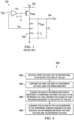
- FIG. 1 is a schematic diagram of an LDO 100.
- the LDO 100 has an input 102 that receives an input voltage V IN at the input 102 during operation of the LDO 100.
- An output 104 provides an output voltage V OUT present during operation of the LDO 100.
- a pass transistor Q PASS is coupled between the input 102 and the output 104.
- a pass voltage across the pass transistor Q PASS is the difference between the input voltage V IN and the output voltage V OUT .
- the minimum pass voltage for sustaining the operation of the LDO 100 is the dropout voltage.
- the LDOs described herein provide stability by way of compensation under load step conditions with high gain, which yields high accuracy.
- the high gain and stability is achieved without the addition of load or compensation capacitors.
- the LDOs provide different gains depending on the difference between the input and output voltages.
- a gain boost amplifier nested within the LDO serves to increase the DC accuracy of the LDO after the load step.
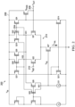
- FIG. 2 is a schematic diagram of an LDO 200 with a class AB input stage 204 and without compensation.
- the LDO 200 is an example of circuitry that may be coupled to the compensation circuits described herein.
- the LDO 200 has an input 206 that is coupled to an input voltage V IN during operation of the LDO 200.
- the LDO 200 generates and regulates an output voltage V OUT at an output 208 during operation of the LDO 200.
- a reference input 210 is coupled to a reference voltage V REF that exists during operation of the LDO 200.
- An error voltage V E (not shown in FIG. 2 ) is the difference between the reference voltage V REF and the output voltage V OUT .
- Transistors Q21 and Q22 form the input of an error amplifier 214 with the gate of transistor Q22 being coupled to the reference voltage V REF and the gate of transistor Q21 being coupled to the output 208.
- the output voltage V OUT is coupled to the error amplifier 214 by way of a voltage divider (not shown), so the voltage received by the error amplifier 214 is proportional to the output voltage V OUT , but not equal to the output voltage V OUT .
- the error amplifier 214 has high input impedances as seen by the reference voltage V REF and the output voltage V OUT .
- the output of the error amplifier 214 is a differential voltage on the drains of transistors Q21 and Q22.
- the voltages on the drains of transistors Q21 and Q22 are referred to individually as VG1 and VG2.
- the gate of the pass transistor Q PASS is driven by the output of the error amplifier 214 by way of transistors Q23 and Q24 that form a portion of a second amplifier.
- the outputs of the error amplifier 214 are coupled to the sources of transistors Q25 and Q26 that form a common gate amplifier. Accordingly, the voltages VG1 and VG2 exist at the sources of transistors Q25 and Q26 during operation of the LDO 200.
- the drains of transistors Q25 and Q26 are coupled to a node N21, which is coupled to a current source I21.
- Node N21 is also coupled to the gate of a transistor Q27, wherein the drain of transistor Q27 is coupled to the sources of transistors Q21 and Q22 in the error amplifier 214.
- the voltage on node N21 and the gate of transistor Q27 is a feedback voltage V FB .
- the source of transistor Q27 is coupled to a node, such as ground as shown in FIG. 2 .
- the current flowing through transistor Q27 is the tail current I TAIL of the error amplifier 214.
- tail current I TAIL refers to the combined currents in the source terminals of the differential pair of transistors Q21 and Q22 in the error amplifier 214.
- Transistors Q23, Q24, Q28, and Q211 are symmetric current mirror loads for the LDO 200.
- Transistors Q213 and Q214 serve as current mirrors for transistors Q211 and Q24.
- the error amplifier 214 operates in a quiescent state in these conditions.
- the voltages VG1 and VG2 set the currents in the error amplifier 214 by setting input stage currents.
- this change in tail current I TAIL results in higher current drive in the input stage to move the gate of the pass transistor Q PASS faster during the load step, so as to minimize transients during the load step.
- Nonlinearity in the LDO 200 is provided by the combination of transistors Q28/Q29 and Q23/Q210 during these conditions. In some examples where the transistors have a ratio of four, an error voltage V E of 100mV has 1000x tail current increase.
- Compensation is achieved by reducing the voltage gain of the input stage 204, depicted as the amplifier 304, by limiting the resistance of a resistor R31 as described herein.
- the resistance R31 is the resistance coupled to the gate of the pass transistor Q PASS .
- Limiting the resistance of resistor R31 reduces the overall gain of the LDO 300, which results in low DC accuracy, but stabilizes the LDO 300.
- Recuperating the voltage gain of the LDO 300 includes nesting of the stages and boosting the gain of an existing, already stable, amplifier, such as the error amplifier 214 described hereinabove. Nesting of the amplifier stages is performed with the LDO 300 rather than cascading gain stages in series as is done in conventional applications.
- the nesting of the amplifiers in the LDO 300 is performed by a gain boost amplifier 314, which recuperates the gain for DC accuracy.
- the amplifier 314 tracks the voltage at its inputs and ensures that the voltage V OUT is equal to the voltage V REF to achieve DC accuracy.
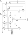
- FIG. 4 is a schematic diagram of an LDO 400 having a gain boost amplifier nested therein and which is an illustrative example not forming part of the claimed invention.
- the LDO 400 has many of the same components as the LDO 200 of FIG. 2 and has the same reference numerals applied to those components.
- the LDO 400 includes a gain boost amplifier 402 having an output coupled to the gate of a transistor Q41.
- Transistor Q41 is coupled between the sources of transistors Q213 and Q214 and the ground node. Accordingly, the current flow through transistors Q213 and Q214 is based on the output of the amplifier 402.
- the inputs of the amplifier 402 are coupled to the gate of transistor Q213 and the drain of transistor Q214, which is coupled to the gate of the pass transistor Q PASS .
- the gain boost amplifier 402 is a tracking amplifier that ensures its inputs always track each other. More specifically, the gain boost amplifier 402 ensures that the voltage at the gate of transistor Q213 and the voltage at the gate of the pass transistor Q PASS track each other. The tracking is achieved by regulating the drain current of transistor Q41, which is achieved by the drive provided to the gate of transistor Q41 by the output of the amplifier 402.
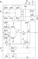
- FIG. 5 is a schematic diagram of an example LDO 500 with the gain boost amplifier 402 nested therein and which is an illustrative example not forming part of the claimed invention.
- the LDO 500 includes the LDO 200 of FIG. 2 with the addition of the gain boost amplifier 402 of FIG. 4 that provides compensation and load stability.
- the LDO 500 includes substantially the same circuitry as the LDO 200 of FIG. 2 with the addition of the gain boost amplifier 402. Compensation in the LDO 500 is achieved by limiting the voltage gain of the error amplifier 214, which is accomplished by limiting the resistance at the gate of the pass transistor Q PASS .
- transistors Q51 and Q52 are biased by a fraction of the currents through transistors Q53 and Q54, which achieves the lower voltage gain in the error amplifier 214. If the voltage gain in the error amplifier 214 is small, the overall gain of the LDO 500 may not be sufficient for acceptable load regulation.
- Transistors Q41 and Q55-Q58 form the gain boosting amplifier. With this gain boosting amplifier, the voltages at the gates of the pass transistor Q PASS and transistor Q213 track each other.
- the gain boosting amplifier 402 is designed to be slowed by the use of resistor R51 and capacitor C51 so that it does not affect the stability of the LDO 500.
- resistor R51 and capacitor C51 form a filter that slows the amplifier 402.
- the filter is not included in the LDO 500.
- FIG. 6 is a flowchart 600 describing a method of compensating an LDO.
- Step 602 of the flowchart 600 includes receiving a first voltage that is proportional to an output voltage of the LDO.
- Step 604 includes comparing the first voltage to a reference voltage using the error amplifier.
- Step 606 includes changing the gain of the error amplifier in response to comparing the first voltage to the reference voltage, wherein the change of gain provides gain boost to the output of the LDO.
- Step 608 includes changing the DC gain of the LDO in response to the comparing, wherein changing the gain reduces the difference between the first voltage and the reference voltage.
Landscapes
- Engineering & Computer Science (AREA)
- Physics & Mathematics (AREA)
- Electromagnetism (AREA)
- General Physics & Mathematics (AREA)
- Radar, Positioning & Navigation (AREA)
- Automation & Control Theory (AREA)
- Power Engineering (AREA)
- Continuous-Control Power Sources That Use Transistors (AREA)
- Amplifiers (AREA)
Applications Claiming Priority (2)
| Application Number | Priority Date | Filing Date | Title |
|---|---|---|---|
| US15/400,976 US11009900B2 (en) | 2017-01-07 | 2017-01-07 | Method and circuitry for compensating low dropout regulators |
| PCT/US2018/012803 WO2018129459A1 (en) | 2017-01-07 | 2018-01-08 | Method and circuitry for compensating low dropout regulators |
Publications (3)
| Publication Number | Publication Date |
|---|---|
| EP3566108A1 EP3566108A1 (en) | 2019-11-13 |
| EP3566108A4 EP3566108A4 (en) | 2021-01-13 |
| EP3566108B1 true EP3566108B1 (en) | 2025-06-25 |
Family
ID=62783042
Family Applications (1)
| Application Number | Title | Priority Date | Filing Date |
|---|---|---|---|
| EP18736064.9A Active EP3566108B1 (en) | 2017-01-07 | 2018-01-08 | Method and circuitry for compensating low dropout regulators |
Country Status (5)
| Country | Link |
|---|---|
| US (1) | US11009900B2 (enExample) |
| EP (1) | EP3566108B1 (enExample) |
| JP (1) | JP7108166B2 (enExample) |
| CN (2) | CN110366713B (enExample) |
| WO (1) | WO2018129459A1 (enExample) |
Families Citing this family (8)
| Publication number | Priority date | Publication date | Assignee | Title |
|---|---|---|---|---|
| WO2019126946A1 (en) * | 2017-12-25 | 2019-07-04 | Texas Instruments Incorporated | Low-dropout regulator with load-adaptive frequency compensation |
| US11487312B2 (en) * | 2020-03-27 | 2022-11-01 | Semiconductor Components Industries, Llc | Compensation for low dropout voltage regulator |
| US11942866B2 (en) * | 2020-09-03 | 2024-03-26 | Cypress Semiconductor Corporation | Transconductance amplifier for buck-boost converter |
| US12040785B2 (en) * | 2021-09-24 | 2024-07-16 | Qualcomm Incorporated | Robust transistor circuitry |
| US12181963B2 (en) | 2021-09-24 | 2024-12-31 | Qualcomm Incorporated | Robust circuitry for passive fundamental components |
| CN114281142B (zh) * | 2021-12-23 | 2023-05-05 | 江苏稻源科技集团有限公司 | 一种高瞬态响应的无片外电容ldo |
| US12334950B2 (en) * | 2022-12-28 | 2025-06-17 | Texas Instruments Incorporated | Dynamic range boost for amplifiers |
| CN119105604A (zh) * | 2024-09-23 | 2024-12-10 | 浙江大学 | 一种兼具拉电流和灌电流能力的ldo电路 |
Family Cites Families (28)
| Publication number | Priority date | Publication date | Assignee | Title |
|---|---|---|---|---|
| US6369618B1 (en) | 1999-02-12 | 2002-04-09 | Texas Instruments Incorporated | Temperature and process independent exponential voltage-to-current converter circuit |
| US6246221B1 (en) * | 2000-09-20 | 2001-06-12 | Texas Instruments Incorporated | PMOS low drop-out voltage regulator using non-inverting variable gain stage |
| JP3574394B2 (ja) * | 2000-10-02 | 2004-10-06 | シャープ株式会社 | スイッチング電源装置 |
| US6600299B2 (en) * | 2001-12-19 | 2003-07-29 | Texas Instruments Incorporated | Miller compensated NMOS low drop-out voltage regulator using variable gain stage |
| EP1336912A1 (en) | 2002-02-18 | 2003-08-20 | Motorola, Inc. | Low drop-out voltage regulator |
| US6703815B2 (en) | 2002-05-20 | 2004-03-09 | Texas Instruments Incorporated | Low drop-out regulator having current feedback amplifier and composite feedback loop |
| JP2004120306A (ja) | 2002-09-26 | 2004-04-15 | Renesas Technology Corp | 利得可変増幅器 |
| US6952091B2 (en) * | 2002-12-10 | 2005-10-04 | Stmicroelectronics Pvt. Ltd. | Integrated low dropout linear voltage regulator with improved current limiting |
| TWI237942B (en) * | 2004-05-06 | 2005-08-11 | Ind Tech Res Inst | Programmable/tunable active RC filter |
| US7075364B2 (en) * | 2004-08-17 | 2006-07-11 | Qualcomm Incorporated | Active-RC filter with compensation to reduce Q enhancement |
| US7495422B2 (en) * | 2005-07-22 | 2009-02-24 | Hong Kong University Of Science And Technology | Area-efficient capacitor-free low-dropout regulator |
| JP2008217677A (ja) * | 2007-03-07 | 2008-09-18 | Ricoh Co Ltd | 定電圧回路及びその動作制御方法 |
| US7768351B2 (en) * | 2008-06-25 | 2010-08-03 | Texas Instruments Incorporated | Variable gain current input amplifier and method |
| US20110101936A1 (en) * | 2008-06-26 | 2011-05-05 | Nxp B.V. | Low dropout voltage regulator and method of stabilising a linear regulator |
| JP5097664B2 (ja) | 2008-09-26 | 2012-12-12 | ラピスセミコンダクタ株式会社 | 定電圧電源回路 |
| JP2011091572A (ja) * | 2009-10-21 | 2011-05-06 | Sanyo Electric Co Ltd | 可変利得増幅回路 |
| US20120212199A1 (en) | 2011-02-22 | 2012-08-23 | Ahmed Amer | Low Drop Out Voltage Regulator |
| US9134743B2 (en) * | 2012-04-30 | 2015-09-15 | Infineon Technologies Austria Ag | Low-dropout voltage regulator |
| US20150015222A1 (en) * | 2013-07-09 | 2015-01-15 | Texas Instruments Deutschland Gmbh | Low dropout voltage regulator |
| EP2887175B1 (en) * | 2013-12-19 | 2017-11-29 | Dialog Semiconductor GmbH | Method and system for gain boosting in linear regulators |
| US9312824B2 (en) * | 2014-01-14 | 2016-04-12 | Intel Deutschland Gmbh | Low noise low-dropout regulator |
| CN104821721B (zh) | 2014-02-05 | 2019-02-05 | 英特赛尔美国有限公司 | 用于低压差(ldo)稳压器中增强型瞬态响应的半导体结构 |
| CN204652316U (zh) * | 2014-12-29 | 2015-09-16 | 意法半导体研发(深圳)有限公司 | 低压差放大器、误差放大器及放大电路 |
| JP2016162097A (ja) * | 2015-02-27 | 2016-09-05 | 株式会社東芝 | 電源回路 |
| CN104777871A (zh) | 2015-05-08 | 2015-07-15 | 苏州大学 | 一种低压差线性稳压器 |
| WO2016202398A1 (en) | 2015-06-18 | 2016-12-22 | Epcos Ag | Low-dropout voltage regulator apparatus |
| CN104950974B (zh) * | 2015-06-30 | 2017-05-31 | 华为技术有限公司 | 低压差线性稳压器与增加其稳定性的方法及锁相环 |
| TWI560538B (en) * | 2015-06-30 | 2016-12-01 | Univ Nat Tsing Hua | Feedback type voltage regulator |
-
2017
- 2017-01-07 US US15/400,976 patent/US11009900B2/en active Active
-
2018
- 2018-01-08 JP JP2019537100A patent/JP7108166B2/ja active Active
- 2018-01-08 CN CN201880014138.3A patent/CN110366713B/zh active Active
- 2018-01-08 EP EP18736064.9A patent/EP3566108B1/en active Active
- 2018-01-08 CN CN202111304847.5A patent/CN113885626B/zh active Active
- 2018-01-08 WO PCT/US2018/012803 patent/WO2018129459A1/en not_active Ceased
Also Published As
| Publication number | Publication date |
|---|---|
| CN113885626A (zh) | 2022-01-04 |
| JP7108166B2 (ja) | 2022-07-28 |
| CN113885626B (zh) | 2023-03-10 |
| CN110366713B (zh) | 2021-11-26 |
| EP3566108A4 (en) | 2021-01-13 |
| CN110366713A (zh) | 2019-10-22 |
| JP2020505679A (ja) | 2020-02-20 |
| WO2018129459A1 (en) | 2018-07-12 |
| EP3566108A1 (en) | 2019-11-13 |
| US20180196454A1 (en) | 2018-07-12 |
| US11009900B2 (en) | 2021-05-18 |
Similar Documents
| Publication | Publication Date | Title |
|---|---|---|
| EP3566108B1 (en) | Method and circuitry for compensating low dropout regulators | |
| US7166991B2 (en) | Adaptive biasing concept for current mode voltage regulators | |
| US6856124B2 (en) | LDO regulator with wide output load range and fast internal loop | |
| US11846956B2 (en) | Linear voltage regulator with stability compensation | |
| US7598716B2 (en) | Low pass filter low drop-out voltage regulator | |
| US7459891B2 (en) | Soft-start circuit and method for low-dropout voltage regulators | |
| US10310530B1 (en) | Low-dropout regulator with load-adaptive frequency compensation | |
| US7091710B2 (en) | Low dropout voltage regulator providing adaptive compensation | |
| US9904305B2 (en) | Voltage regulator with adaptive bias network | |
| US20050184711A1 (en) | Low dropout voltage regulator | |
| EP3311235B1 (en) | Low-dropout voltage regulator apparatus | |
| US20130241504A1 (en) | Self-calibrating, stable ldo regulator | |
| US9831757B2 (en) | Voltage regulator | |
| EP1947544A1 (en) | Voltage regulator and method for voltage regulation | |
| Montalvo-Galicia et al. | Comparison of two internal miller compensation techniques for LDO regulators | |
| US20070257644A1 (en) | Voltage regulator with inherent voltage clamping | |
| US20100327830A1 (en) | Low voltage drop out regulator | |
| US9886052B2 (en) | Voltage regulator | |
| US9128505B2 (en) | Voltage regulator circuit | |
| US10649480B2 (en) | Voltage regulator | |
| US7956588B2 (en) | Voltage regulator | |
| US20150097543A1 (en) | Voltage regulator | |
| CN114356008A (zh) | 一种低压差线性稳压器 | |
| US8253479B2 (en) | Output driver circuits for voltage regulators | |
| KR102960383B1 (ko) | 과도 전류 센싱 구조를 이용한 ldo 레귤레이터 |
Legal Events
| Date | Code | Title | Description |
|---|---|---|---|
| STAA | Information on the status of an ep patent application or granted ep patent |
Free format text: STATUS: THE INTERNATIONAL PUBLICATION HAS BEEN MADE |
|
| PUAI | Public reference made under article 153(3) epc to a published international application that has entered the european phase |
Free format text: ORIGINAL CODE: 0009012 |
|
| STAA | Information on the status of an ep patent application or granted ep patent |
Free format text: STATUS: REQUEST FOR EXAMINATION WAS MADE |
|
| 17P | Request for examination filed |
Effective date: 20190807 |
|
| AK | Designated contracting states |
Kind code of ref document: A1 Designated state(s): AL AT BE BG CH CY CZ DE DK EE ES FI FR GB GR HR HU IE IS IT LI LT LU LV MC MK MT NL NO PL PT RO RS SE SI SK SM TR |
|
| AX | Request for extension of the european patent |
Extension state: BA ME |
|
| DAV | Request for validation of the european patent (deleted) | ||
| DAX | Request for extension of the european patent (deleted) | ||
| RIC1 | Information provided on ipc code assigned before grant |
Ipc: G05F 1/575 20060101AFI20200716BHEP Ipc: G05F 1/563 20060101ALI20200716BHEP |
|
| A4 | Supplementary search report drawn up and despatched |
Effective date: 20201215 |
|
| RIC1 | Information provided on ipc code assigned before grant |
Ipc: G05F 1/563 20060101ALI20201209BHEP Ipc: G05F 1/575 20060101AFI20201209BHEP |
|
| STAA | Information on the status of an ep patent application or granted ep patent |
Free format text: STATUS: EXAMINATION IS IN PROGRESS |
|
| 17Q | First examination report despatched |
Effective date: 20221222 |
|
| GRAP | Despatch of communication of intention to grant a patent |
Free format text: ORIGINAL CODE: EPIDOSNIGR1 |
|
| STAA | Information on the status of an ep patent application or granted ep patent |
Free format text: STATUS: GRANT OF PATENT IS INTENDED |
|
| INTG | Intention to grant announced |
Effective date: 20250129 |
|
| GRAS | Grant fee paid |
Free format text: ORIGINAL CODE: EPIDOSNIGR3 |
|
| GRAA | (expected) grant |
Free format text: ORIGINAL CODE: 0009210 |
|
| STAA | Information on the status of an ep patent application or granted ep patent |
Free format text: STATUS: THE PATENT HAS BEEN GRANTED |
|
| P01 | Opt-out of the competence of the unified patent court (upc) registered |
Free format text: CASE NUMBER: APP_20664/2025 Effective date: 20250430 |
|
| AK | Designated contracting states |
Kind code of ref document: B1 Designated state(s): AL AT BE BG CH CY CZ DE DK EE ES FI FR GB GR HR HU IE IS IT LI LT LU LV MC MK MT NL NO PL PT RO RS SE SI SK SM TR |
|
| REG | Reference to a national code |
Ref country code: GB Ref legal event code: FG4D |
|
| REG | Reference to a national code |
Ref country code: CH Ref legal event code: EP |
|
| REG | Reference to a national code |
Ref country code: CH Ref legal event code: EP |
|
| REG | Reference to a national code |
Ref country code: IE Ref legal event code: FG4D |
|
| REG | Reference to a national code |
Ref country code: DE Ref legal event code: R096 Ref document number: 602018082902 Country of ref document: DE |
|
| PG25 | Lapsed in a contracting state [announced via postgrant information from national office to epo] |
Ref country code: FI Free format text: LAPSE BECAUSE OF FAILURE TO SUBMIT A TRANSLATION OF THE DESCRIPTION OR TO PAY THE FEE WITHIN THE PRESCRIBED TIME-LIMIT Effective date: 20250625 |
|
| REG | Reference to a national code |
Ref country code: LT Ref legal event code: MG9D |
|
| PG25 | Lapsed in a contracting state [announced via postgrant information from national office to epo] |
Ref country code: GR Free format text: LAPSE BECAUSE OF FAILURE TO SUBMIT A TRANSLATION OF THE DESCRIPTION OR TO PAY THE FEE WITHIN THE PRESCRIBED TIME-LIMIT Effective date: 20250926 Ref country code: NO Free format text: LAPSE BECAUSE OF FAILURE TO SUBMIT A TRANSLATION OF THE DESCRIPTION OR TO PAY THE FEE WITHIN THE PRESCRIBED TIME-LIMIT Effective date: 20250925 |
|
| PG25 | Lapsed in a contracting state [announced via postgrant information from national office to epo] |
Ref country code: BG Free format text: LAPSE BECAUSE OF FAILURE TO SUBMIT A TRANSLATION OF THE DESCRIPTION OR TO PAY THE FEE WITHIN THE PRESCRIBED TIME-LIMIT Effective date: 20250625 |
|
| PG25 | Lapsed in a contracting state [announced via postgrant information from national office to epo] |
Ref country code: HR Free format text: LAPSE BECAUSE OF FAILURE TO SUBMIT A TRANSLATION OF THE DESCRIPTION OR TO PAY THE FEE WITHIN THE PRESCRIBED TIME-LIMIT Effective date: 20250625 |
|
| PG25 | Lapsed in a contracting state [announced via postgrant information from national office to epo] |
Ref country code: RS Free format text: LAPSE BECAUSE OF FAILURE TO SUBMIT A TRANSLATION OF THE DESCRIPTION OR TO PAY THE FEE WITHIN THE PRESCRIBED TIME-LIMIT Effective date: 20250925 |
|
| PG25 | Lapsed in a contracting state [announced via postgrant information from national office to epo] |
Ref country code: LV Free format text: LAPSE BECAUSE OF FAILURE TO SUBMIT A TRANSLATION OF THE DESCRIPTION OR TO PAY THE FEE WITHIN THE PRESCRIBED TIME-LIMIT Effective date: 20250625 |
|
| REG | Reference to a national code |
Ref country code: NL Ref legal event code: MP Effective date: 20250625 |
|
| PG25 | Lapsed in a contracting state [announced via postgrant information from national office to epo] |
Ref country code: NL Free format text: LAPSE BECAUSE OF FAILURE TO SUBMIT A TRANSLATION OF THE DESCRIPTION OR TO PAY THE FEE WITHIN THE PRESCRIBED TIME-LIMIT Effective date: 20250625 |
|
| PG25 | Lapsed in a contracting state [announced via postgrant information from national office to epo] |
Ref country code: PT Free format text: LAPSE BECAUSE OF FAILURE TO SUBMIT A TRANSLATION OF THE DESCRIPTION OR TO PAY THE FEE WITHIN THE PRESCRIBED TIME-LIMIT Effective date: 20251027 |
|
| REG | Reference to a national code |
Ref country code: AT Ref legal event code: MK05 Ref document number: 1807114 Country of ref document: AT Kind code of ref document: T Effective date: 20250625 |
|
| PG25 | Lapsed in a contracting state [announced via postgrant information from national office to epo] |
Ref country code: IS Free format text: LAPSE BECAUSE OF FAILURE TO SUBMIT A TRANSLATION OF THE DESCRIPTION OR TO PAY THE FEE WITHIN THE PRESCRIBED TIME-LIMIT Effective date: 20251025 |
|
| PGFP | Annual fee paid to national office [announced via postgrant information from national office to epo] |
Ref country code: GB Payment date: 20251219 Year of fee payment: 9 |
|
| PG25 | Lapsed in a contracting state [announced via postgrant information from national office to epo] |
Ref country code: AT Free format text: LAPSE BECAUSE OF FAILURE TO SUBMIT A TRANSLATION OF THE DESCRIPTION OR TO PAY THE FEE WITHIN THE PRESCRIBED TIME-LIMIT Effective date: 20250625 Ref country code: SM Free format text: LAPSE BECAUSE OF FAILURE TO SUBMIT A TRANSLATION OF THE DESCRIPTION OR TO PAY THE FEE WITHIN THE PRESCRIBED TIME-LIMIT Effective date: 20250625 |
|
| PGFP | Annual fee paid to national office [announced via postgrant information from national office to epo] |
Ref country code: FR Payment date: 20251217 Year of fee payment: 9 |
|
| PG25 | Lapsed in a contracting state [announced via postgrant information from national office to epo] |
Ref country code: CZ Free format text: LAPSE BECAUSE OF FAILURE TO SUBMIT A TRANSLATION OF THE DESCRIPTION OR TO PAY THE FEE WITHIN THE PRESCRIBED TIME-LIMIT Effective date: 20250625 |
|
| PG25 | Lapsed in a contracting state [announced via postgrant information from national office to epo] |
Ref country code: PL Free format text: LAPSE BECAUSE OF FAILURE TO SUBMIT A TRANSLATION OF THE DESCRIPTION OR TO PAY THE FEE WITHIN THE PRESCRIBED TIME-LIMIT Effective date: 20250625 |
|
| PG25 | Lapsed in a contracting state [announced via postgrant information from national office to epo] |
Ref country code: EE Free format text: LAPSE BECAUSE OF FAILURE TO SUBMIT A TRANSLATION OF THE DESCRIPTION OR TO PAY THE FEE WITHIN THE PRESCRIBED TIME-LIMIT Effective date: 20250625 |
|
| PG25 | Lapsed in a contracting state [announced via postgrant information from national office to epo] |
Ref country code: SK Free format text: LAPSE BECAUSE OF FAILURE TO SUBMIT A TRANSLATION OF THE DESCRIPTION OR TO PAY THE FEE WITHIN THE PRESCRIBED TIME-LIMIT Effective date: 20250625 |
|
| PG25 | Lapsed in a contracting state [announced via postgrant information from national office to epo] |
Ref country code: ES Free format text: LAPSE BECAUSE OF FAILURE TO SUBMIT A TRANSLATION OF THE DESCRIPTION OR TO PAY THE FEE WITHIN THE PRESCRIBED TIME-LIMIT Effective date: 20250625 |
|
| PG25 | Lapsed in a contracting state [announced via postgrant information from national office to epo] |
Ref country code: DK Free format text: LAPSE BECAUSE OF FAILURE TO SUBMIT A TRANSLATION OF THE DESCRIPTION OR TO PAY THE FEE WITHIN THE PRESCRIBED TIME-LIMIT Effective date: 20250625 |
|
| PGFP | Annual fee paid to national office [announced via postgrant information from national office to epo] |
Ref country code: DE Payment date: 20251217 Year of fee payment: 9 |
|
| PG25 | Lapsed in a contracting state [announced via postgrant information from national office to epo] |
Ref country code: IT Free format text: LAPSE BECAUSE OF FAILURE TO SUBMIT A TRANSLATION OF THE DESCRIPTION OR TO PAY THE FEE WITHIN THE PRESCRIBED TIME-LIMIT Effective date: 20250625 |
|
| PLBE | No opposition filed within time limit |
Free format text: ORIGINAL CODE: 0009261 |
|
| STAA | Information on the status of an ep patent application or granted ep patent |
Free format text: STATUS: NO OPPOSITION FILED WITHIN TIME LIMIT |