EP3564935A1 - K-wert-messverfahren für einen oled-ansteuernden dünnschichttransistor - Google Patents
K-wert-messverfahren für einen oled-ansteuernden dünnschichttransistor Download PDFInfo
- Publication number
- EP3564935A1 EP3564935A1 EP17888832.7A EP17888832A EP3564935A1 EP 3564935 A1 EP3564935 A1 EP 3564935A1 EP 17888832 A EP17888832 A EP 17888832A EP 3564935 A1 EP3564935 A1 EP 3564935A1
- Authority
- EP
- European Patent Office
- Prior art keywords
- thin film
- film transistor
- data
- current
- value
- Prior art date
- Legal status (The legal status is an assumption and is not a legal conclusion. Google has not performed a legal analysis and makes no representation as to the accuracy of the status listed.)
- Granted
Links
- 239000010409 thin film Substances 0.000 title claims abstract description 263
- 238000000034 method Methods 0.000 title claims abstract description 77
- 238000001514 detection method Methods 0.000 claims description 78
- 230000010354 integration Effects 0.000 claims description 19
- 239000003990 capacitor Substances 0.000 claims description 11
- 230000003071 parasitic effect Effects 0.000 claims description 8
- 239000004065 semiconductor Substances 0.000 claims description 7
- 229910021417 amorphous silicon Inorganic materials 0.000 claims description 5
- 230000002596 correlated effect Effects 0.000 claims description 5
- 229910021420 polycrystalline silicon Inorganic materials 0.000 claims description 5
- 229920005591 polysilicon Polymers 0.000 claims description 5
- 230000000694 effects Effects 0.000 abstract description 2
- 229920001621 AMOLED Polymers 0.000 description 7
- 238000002347 injection Methods 0.000 description 5
- 239000007924 injection Substances 0.000 description 5
- 230000001737 promoting effect Effects 0.000 description 4
- 238000009795 derivation Methods 0.000 description 2
- 238000010586 diagram Methods 0.000 description 2
- 238000005286 illumination Methods 0.000 description 2
- 239000000463 material Substances 0.000 description 2
- 239000011159 matrix material Substances 0.000 description 2
- 239000000758 substrate Substances 0.000 description 2
- 230000032683 aging Effects 0.000 description 1
- 230000005684 electric field Effects 0.000 description 1
- 238000005516 engineering process Methods 0.000 description 1
- AMGQUBHHOARCQH-UHFFFAOYSA-N indium;oxotin Chemical compound [In].[Sn]=O AMGQUBHHOARCQH-UHFFFAOYSA-N 0.000 description 1
- 238000004020 luminiscence type Methods 0.000 description 1
- 229910052751 metal Inorganic materials 0.000 description 1
- 239000002184 metal Substances 0.000 description 1
- 238000005215 recombination Methods 0.000 description 1
- 230000006798 recombination Effects 0.000 description 1
- 239000000243 solution Substances 0.000 description 1
- 238000006467 substitution reaction Methods 0.000 description 1
Images

Classifications
-
- G—PHYSICS
- G09—EDUCATION; CRYPTOGRAPHY; DISPLAY; ADVERTISING; SEALS
- G09G—ARRANGEMENTS OR CIRCUITS FOR CONTROL OF INDICATING DEVICES USING STATIC MEANS TO PRESENT VARIABLE INFORMATION
- G09G3/00—Control arrangements or circuits, of interest only in connection with visual indicators other than cathode-ray tubes
- G09G3/006—Electronic inspection or testing of displays and display drivers, e.g. of LED or LCD displays
-
- G—PHYSICS
- G09—EDUCATION; CRYPTOGRAPHY; DISPLAY; ADVERTISING; SEALS
- G09G—ARRANGEMENTS OR CIRCUITS FOR CONTROL OF INDICATING DEVICES USING STATIC MEANS TO PRESENT VARIABLE INFORMATION
- G09G3/00—Control arrangements or circuits, of interest only in connection with visual indicators other than cathode-ray tubes
- G09G3/20—Control arrangements or circuits, of interest only in connection with visual indicators other than cathode-ray tubes for presentation of an assembly of a number of characters, e.g. a page, by composing the assembly by combination of individual elements arranged in a matrix no fixed position being assigned to or needed to be assigned to the individual characters or partial characters
- G09G3/22—Control arrangements or circuits, of interest only in connection with visual indicators other than cathode-ray tubes for presentation of an assembly of a number of characters, e.g. a page, by composing the assembly by combination of individual elements arranged in a matrix no fixed position being assigned to or needed to be assigned to the individual characters or partial characters using controlled light sources
- G09G3/30—Control arrangements or circuits, of interest only in connection with visual indicators other than cathode-ray tubes for presentation of an assembly of a number of characters, e.g. a page, by composing the assembly by combination of individual elements arranged in a matrix no fixed position being assigned to or needed to be assigned to the individual characters or partial characters using controlled light sources using electroluminescent panels
- G09G3/32—Control arrangements or circuits, of interest only in connection with visual indicators other than cathode-ray tubes for presentation of an assembly of a number of characters, e.g. a page, by composing the assembly by combination of individual elements arranged in a matrix no fixed position being assigned to or needed to be assigned to the individual characters or partial characters using controlled light sources using electroluminescent panels semiconductive, e.g. using light-emitting diodes [LED]
- G09G3/3208—Control arrangements or circuits, of interest only in connection with visual indicators other than cathode-ray tubes for presentation of an assembly of a number of characters, e.g. a page, by composing the assembly by combination of individual elements arranged in a matrix no fixed position being assigned to or needed to be assigned to the individual characters or partial characters using controlled light sources using electroluminescent panels semiconductive, e.g. using light-emitting diodes [LED] organic, e.g. using organic light-emitting diodes [OLED]
- G09G3/3225—Control arrangements or circuits, of interest only in connection with visual indicators other than cathode-ray tubes for presentation of an assembly of a number of characters, e.g. a page, by composing the assembly by combination of individual elements arranged in a matrix no fixed position being assigned to or needed to be assigned to the individual characters or partial characters using controlled light sources using electroluminescent panels semiconductive, e.g. using light-emitting diodes [LED] organic, e.g. using organic light-emitting diodes [OLED] using an active matrix
- G09G3/3233—Control arrangements or circuits, of interest only in connection with visual indicators other than cathode-ray tubes for presentation of an assembly of a number of characters, e.g. a page, by composing the assembly by combination of individual elements arranged in a matrix no fixed position being assigned to or needed to be assigned to the individual characters or partial characters using controlled light sources using electroluminescent panels semiconductive, e.g. using light-emitting diodes [LED] organic, e.g. using organic light-emitting diodes [OLED] using an active matrix with pixel circuitry controlling the current through the light-emitting element
-
- G—PHYSICS
- G09—EDUCATION; CRYPTOGRAPHY; DISPLAY; ADVERTISING; SEALS
- G09G—ARRANGEMENTS OR CIRCUITS FOR CONTROL OF INDICATING DEVICES USING STATIC MEANS TO PRESENT VARIABLE INFORMATION
- G09G3/00—Control arrangements or circuits, of interest only in connection with visual indicators other than cathode-ray tubes
- G09G3/20—Control arrangements or circuits, of interest only in connection with visual indicators other than cathode-ray tubes for presentation of an assembly of a number of characters, e.g. a page, by composing the assembly by combination of individual elements arranged in a matrix no fixed position being assigned to or needed to be assigned to the individual characters or partial characters
- G09G3/22—Control arrangements or circuits, of interest only in connection with visual indicators other than cathode-ray tubes for presentation of an assembly of a number of characters, e.g. a page, by composing the assembly by combination of individual elements arranged in a matrix no fixed position being assigned to or needed to be assigned to the individual characters or partial characters using controlled light sources
- G09G3/30—Control arrangements or circuits, of interest only in connection with visual indicators other than cathode-ray tubes for presentation of an assembly of a number of characters, e.g. a page, by composing the assembly by combination of individual elements arranged in a matrix no fixed position being assigned to or needed to be assigned to the individual characters or partial characters using controlled light sources using electroluminescent panels
- G09G3/32—Control arrangements or circuits, of interest only in connection with visual indicators other than cathode-ray tubes for presentation of an assembly of a number of characters, e.g. a page, by composing the assembly by combination of individual elements arranged in a matrix no fixed position being assigned to or needed to be assigned to the individual characters or partial characters using controlled light sources using electroluminescent panels semiconductive, e.g. using light-emitting diodes [LED]
- G09G3/3208—Control arrangements or circuits, of interest only in connection with visual indicators other than cathode-ray tubes for presentation of an assembly of a number of characters, e.g. a page, by composing the assembly by combination of individual elements arranged in a matrix no fixed position being assigned to or needed to be assigned to the individual characters or partial characters using controlled light sources using electroluminescent panels semiconductive, e.g. using light-emitting diodes [LED] organic, e.g. using organic light-emitting diodes [OLED]
- G09G3/3225—Control arrangements or circuits, of interest only in connection with visual indicators other than cathode-ray tubes for presentation of an assembly of a number of characters, e.g. a page, by composing the assembly by combination of individual elements arranged in a matrix no fixed position being assigned to or needed to be assigned to the individual characters or partial characters using controlled light sources using electroluminescent panels semiconductive, e.g. using light-emitting diodes [LED] organic, e.g. using organic light-emitting diodes [OLED] using an active matrix
- G09G3/3258—Control arrangements or circuits, of interest only in connection with visual indicators other than cathode-ray tubes for presentation of an assembly of a number of characters, e.g. a page, by composing the assembly by combination of individual elements arranged in a matrix no fixed position being assigned to or needed to be assigned to the individual characters or partial characters using controlled light sources using electroluminescent panels semiconductive, e.g. using light-emitting diodes [LED] organic, e.g. using organic light-emitting diodes [OLED] using an active matrix with pixel circuitry controlling the voltage across the light-emitting element
-
- G—PHYSICS
- G09—EDUCATION; CRYPTOGRAPHY; DISPLAY; ADVERTISING; SEALS
- G09G—ARRANGEMENTS OR CIRCUITS FOR CONTROL OF INDICATING DEVICES USING STATIC MEANS TO PRESENT VARIABLE INFORMATION
- G09G3/00—Control arrangements or circuits, of interest only in connection with visual indicators other than cathode-ray tubes
- G09G3/20—Control arrangements or circuits, of interest only in connection with visual indicators other than cathode-ray tubes for presentation of an assembly of a number of characters, e.g. a page, by composing the assembly by combination of individual elements arranged in a matrix no fixed position being assigned to or needed to be assigned to the individual characters or partial characters
- G09G3/22—Control arrangements or circuits, of interest only in connection with visual indicators other than cathode-ray tubes for presentation of an assembly of a number of characters, e.g. a page, by composing the assembly by combination of individual elements arranged in a matrix no fixed position being assigned to or needed to be assigned to the individual characters or partial characters using controlled light sources
- G09G3/30—Control arrangements or circuits, of interest only in connection with visual indicators other than cathode-ray tubes for presentation of an assembly of a number of characters, e.g. a page, by composing the assembly by combination of individual elements arranged in a matrix no fixed position being assigned to or needed to be assigned to the individual characters or partial characters using controlled light sources using electroluminescent panels
- G09G3/32—Control arrangements or circuits, of interest only in connection with visual indicators other than cathode-ray tubes for presentation of an assembly of a number of characters, e.g. a page, by composing the assembly by combination of individual elements arranged in a matrix no fixed position being assigned to or needed to be assigned to the individual characters or partial characters using controlled light sources using electroluminescent panels semiconductive, e.g. using light-emitting diodes [LED]
- G09G3/3208—Control arrangements or circuits, of interest only in connection with visual indicators other than cathode-ray tubes for presentation of an assembly of a number of characters, e.g. a page, by composing the assembly by combination of individual elements arranged in a matrix no fixed position being assigned to or needed to be assigned to the individual characters or partial characters using controlled light sources using electroluminescent panels semiconductive, e.g. using light-emitting diodes [LED] organic, e.g. using organic light-emitting diodes [OLED]
- G09G3/3275—Details of drivers for data electrodes
- G09G3/3291—Details of drivers for data electrodes in which the data driver supplies a variable data voltage for setting the current through, or the voltage across, the light-emitting elements
-
- H—ELECTRICITY
- H10—SEMICONDUCTOR DEVICES; ELECTRIC SOLID-STATE DEVICES NOT OTHERWISE PROVIDED FOR
- H10K—ORGANIC ELECTRIC SOLID-STATE DEVICES
- H10K59/00—Integrated devices, or assemblies of multiple devices, comprising at least one organic light-emitting element covered by group H10K50/00
- H10K59/10—OLED displays
- H10K59/12—Active-matrix OLED [AMOLED] displays
- H10K59/121—Active-matrix OLED [AMOLED] displays characterised by the geometry or disposition of pixel elements
- H10K59/1213—Active-matrix OLED [AMOLED] displays characterised by the geometry or disposition of pixel elements the pixel elements being TFTs
-
- G—PHYSICS
- G09—EDUCATION; CRYPTOGRAPHY; DISPLAY; ADVERTISING; SEALS
- G09G—ARRANGEMENTS OR CIRCUITS FOR CONTROL OF INDICATING DEVICES USING STATIC MEANS TO PRESENT VARIABLE INFORMATION
- G09G2310/00—Command of the display device
- G09G2310/02—Addressing, scanning or driving the display screen or processing steps related thereto
- G09G2310/0262—The addressing of the pixel, in a display other than an active matrix LCD, involving the control of two or more scan electrodes or two or more data electrodes, e.g. pixel voltage dependent on signals of two data electrodes
-
- G—PHYSICS
- G09—EDUCATION; CRYPTOGRAPHY; DISPLAY; ADVERTISING; SEALS
- G09G—ARRANGEMENTS OR CIRCUITS FOR CONTROL OF INDICATING DEVICES USING STATIC MEANS TO PRESENT VARIABLE INFORMATION
- G09G2320/00—Control of display operating conditions
- G09G2320/02—Improving the quality of display appearance
- G09G2320/029—Improving the quality of display appearance by monitoring one or more pixels in the display panel, e.g. by monitoring a fixed reference pixel
- G09G2320/0295—Improving the quality of display appearance by monitoring one or more pixels in the display panel, e.g. by monitoring a fixed reference pixel by monitoring each display pixel
-
- G—PHYSICS
- G09—EDUCATION; CRYPTOGRAPHY; DISPLAY; ADVERTISING; SEALS
- G09G—ARRANGEMENTS OR CIRCUITS FOR CONTROL OF INDICATING DEVICES USING STATIC MEANS TO PRESENT VARIABLE INFORMATION
- G09G2320/00—Control of display operating conditions
- G09G2320/04—Maintaining the quality of display appearance
- G09G2320/043—Preventing or counteracting the effects of ageing
- G09G2320/045—Compensation of drifts in the characteristics of light emitting or modulating elements
Definitions
- the present invention relates to a display technology field, and more particularly to a K value detection method of an OLED drive thin film transistor.
- the Organic Light Emitting Display (OLED) possesses many outstanding properties of self-illumination, low driving voltage, high luminescence efficiency, short response time, high clarity and contrast, near 180° view angle, wide range of working temperature, applicability of flexible display and large scale full color display.
- the OLED is considered as the most potential display device.
- the OLED display device generally comprises a substrate, an anode located on the substrate, a Hole Injection Layer located on the anode, a Hole Transporting Layer located on the Hole Injection Layer, an emitting layer located on the Hole Transporting Layer, an Electron Transport Layer located on the emitting layer, an Electron Injection Layer located on the Electron Transport Layer and a Cathode located on the Electron Injection Layer.
- the principle of the OLED is that the illumination generates due to the carrier injection and recombination under the electric field driving of the semiconductor material and the organic semiconductor illuminating material.
- the (Indium Tin Oxide) ITO pixel electrode and the metal electrode are respectively employed as the anode and the cathode of the Display.
- the Electron and the Hole are respectively injected into the Electron and Hole Transporting Layers from the cathode and the anode.
- the Electron and the Hole respectively migrate from the Electron and Hole Transporting Layers to the Emitting layer and bump into each other in the Emitting layer to form an exciton to excite the emitting molecule.
- the latter can illuminate after the radiative relaxation.
- the OLED can be categorized into two major types according to the driving methods, which are the Passive Matrix OLED (PMOLED) and the Active Matrix OLED (AMOLED), i.e. two types of the direct addressing and the Thin Film Transistor (TFT) matrix addressing.
- the AMOLED comprises pixels arranged in array and belongs to active display type, which has high lighting efficiency and is generally utilized for the large scale display devices of high resolution.
- the AMOLED is a current driving element.
- the organic light emitting diode emits light, and the brightness is determined according to the current flowing through the organic light emitting diode itself.
- Most of the present Integrated Circuits (IC) only transmit voltage signals. Therefore, the AMOLED pixel driving circuit needs to accomplish the task of converting the voltage signals into the current signals.
- the traditional AMOLED pixel driving circuit generally is 2T1C, which is a structure comprising two thin film transistors and one capacitor to convert the voltage into the current.
- the AMOLED pixel driving circuit comprises a drive thin film transistor of driving the organic light emitting diode to emit light.
- the prior art compensates the threshold voltage of the drive thin film transistor during use of the OLED display device.
- An objective of the present invention is to provide a K value detection method of an OLED drive thin film transistor, which can accurately detect the K value of the OLED drive thin film transistor to improve the K value compensation result of the OLED drive thin film transistor for promoting the OLED display quality.
- the present invention provides a K value detection method of an OLED drive thin film transistor, comprising steps of:
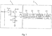
- a process of detecting the current flowing through the second thin film transistor is: first, the current integrator integrating the current flowing through the second thin film transistor, and after integration of the current integrator is accomplished, the CDS sampler collecting an output of the current integrator, and then the analog to digital converter converting an output of an analog signal into a digital signal to obtain the current data and saving the current data in the central process unit.
- I ds Data I ⁇ C / ⁇ ⁇ T ; wherein I ds is the current flowing through the second thin film transistor, and Data I is the current data.
- the central process unit is a FPGA process system.
- a parasitic capacitance is further formed in the sub pixel driving circuit, and the parasitic capacitance is coupled with two ends of the organic light emitting diode in parallel.
- the K value detection method of the OLED drive thin film transistor further comprises: step S5, repeating steps S2 to S4 a plurality of times to perform multiple detections to obtain a plurality of K values of the second thin film transistor, and taking an average value of the plurality of K values of the second thin film transistor as a final K value of the second thin film transistor.
- a different first data voltage and a different second data voltage are used for each detection.
- the first thin film transistor, the second thin film transistor and the third thin film transistor are low temperature polysilicon thin film transistors, amorphous silicon thin film transistors or oxide semiconductor thin film transistors.
- the detected K value of the second thin film transistor is used for compensation for the K value of the second thin film transistor.
- the present invention further provides a K value detection method of an OLED drive thin film transistor, comprising steps of:
- the present invention provides a K value detection method of an OLED drive thin film transistor, comprising steps of:
- I ds K(V gs -V th )2
- K is a constant
- V th is a threshold voltage of the drive thin film transistor
- I ds1 K(V gs1 -V th ) 2
- I ds2 K(V gs2 -V th ) 2
- the present invention further comprises: step 5, repeating steps S2 to S4 a plurality of times to perform multiple detections to obtain a plurality of K values of the second thin film transistor T2, and taking an average value of the plurality of K values of the second thin film transistor T2 as a final K value of the second thin film transistor T2.
- Step 5 uses the method of repeating steps S2 to S4 a plurality of times to perform multiple detections and take the average value.
- the accuracy of the acquired K value of the second thin film transistor T2 can be further promoted to improve the K value compensation result of the OLED drive thin film transistor for promoting the OLED display quality.
- a different first data voltage and a different second data voltage need to be used for each detection in general.
- the K value of the second thin film transistor T2 detected by the present invention can be used for compensation for the K value of the second thin film transistor T2. Because the detected K value of the second thin film transistor T2 is more accurate, the compensation result is better, and the OLED display quality is better.
- the present invention provides a K value detection method of an OLED drive thin film transistor.
- the method sets the data signal to provide two different data voltages to make the drive thin film transistor form two different gate-source voltages, and then the currents flowing through the drive thin film transistor under the two different gate-source voltages are detected by the external detection process circuit, and the central process unit calculates and obtains the K value of the OLED drive thin film transistor according to the two gate-source voltages, the two current data and the formula based on the current formula for the driving thin film transistor.
- the present invention can accurately acquire the K value of the drive thin film transistor of each pixel in the OLED display element to improve the K value compensation result of the OLED drive thin film transistor for promoting the OLED display quality.
Landscapes
- Engineering & Computer Science (AREA)
- Physics & Mathematics (AREA)
- Computer Hardware Design (AREA)
- General Physics & Mathematics (AREA)
- Theoretical Computer Science (AREA)
- Geometry (AREA)
- Microelectronics & Electronic Packaging (AREA)
- Electroluminescent Light Sources (AREA)
- Control Of Indicators Other Than Cathode Ray Tubes (AREA)
- Control Of El Displays (AREA)
Applications Claiming Priority (2)
| Application Number | Priority Date | Filing Date | Title |
|---|---|---|---|
| CN201611247314.7A CN106531041B (zh) | 2016-12-29 | 2016-12-29 | Oled驱动薄膜晶体管的k值侦测方法 |
| PCT/CN2017/073622 WO2018120368A1 (zh) | 2016-12-29 | 2017-02-15 | Oled驱动薄膜晶体管的k值侦测方法 |
Publications (3)
| Publication Number | Publication Date |
|---|---|
| EP3564935A1 true EP3564935A1 (de) | 2019-11-06 |
| EP3564935A4 EP3564935A4 (de) | 2020-05-13 |
| EP3564935B1 EP3564935B1 (de) | 2021-10-06 |
Family
ID=58339140
Family Applications (1)
| Application Number | Title | Priority Date | Filing Date |
|---|---|---|---|
| EP17888832.7A Not-in-force EP3564935B1 (de) | 2016-12-29 | 2017-02-15 | K-wert-messverfahren für einen oled-ansteuernden dünnschichttransistor |
Country Status (6)
| Country | Link |
|---|---|
| US (1) | US10102784B2 (de) |
| EP (1) | EP3564935B1 (de) |
| JP (1) | JP2020515883A (de) |
| KR (1) | KR102232040B1 (de) |
| CN (1) | CN106531041B (de) |
| WO (1) | WO2018120368A1 (de) |
Families Citing this family (13)
| Publication number | Priority date | Publication date | Assignee | Title |
|---|---|---|---|---|
| CN107507572B (zh) * | 2017-09-01 | 2019-10-11 | 深圳市华星光电半导体显示技术有限公司 | Oled驱动薄膜晶体管的参数获取方法 |
| CN109671393B (zh) | 2017-10-13 | 2020-07-31 | 京东方科技集团股份有限公司 | 一种像素补偿方法及系统、显示装置 |
| CN107516484B (zh) * | 2017-10-18 | 2019-10-11 | 深圳市华星光电半导体显示技术有限公司 | Amoled外部电学补偿侦测方法 |
| CN107784971A (zh) * | 2017-10-31 | 2018-03-09 | 昆山国显光电有限公司 | 异形显示屏和集成异形显示屏的显示装置 |
| CN107909965B (zh) * | 2017-12-07 | 2019-08-13 | 京东方科技集团股份有限公司 | 用于显示面板的补偿方法和装置 |
| CN108109588B (zh) * | 2018-01-10 | 2019-11-05 | 京东方科技集团股份有限公司 | 电压采集电路及方法、外部补偿电路及显示装置 |
| CN109935182B (zh) * | 2018-07-27 | 2020-07-17 | 京东方科技集团股份有限公司 | 像素电流检测电路、方法、显示装置 |
| CN110767132B (zh) * | 2019-10-25 | 2021-02-02 | 深圳市华星光电半导体显示技术有限公司 | Tft电性侦测校正方法、装置、系统及显示装置 |
| CN112863444B (zh) * | 2021-01-13 | 2022-05-03 | 深圳市华星光电半导体显示技术有限公司 | 驱动电路的补偿电压计算方法 |
| CN113257184B (zh) | 2021-05-10 | 2022-10-25 | 京东方科技集团股份有限公司 | 采样电路及驱动方法、像素采样电路、显示装置 |
| CN114882842B (zh) * | 2022-05-05 | 2024-01-19 | 云谷(固安)科技有限公司 | 显示驱动方法、装置、设备及存储介质 |
| US11568813B1 (en) * | 2022-05-10 | 2023-01-31 | Meta Platforms Technologies, Llc | Pixel level burn-in compensation for light-emitting diode based displays |
| CN119152810A (zh) * | 2024-09-29 | 2024-12-17 | 合肥维信诺科技有限公司 | 像素电路的驱动方法、显示装置及其驱动方法 |
Family Cites Families (17)
| Publication number | Priority date | Publication date | Assignee | Title |
|---|---|---|---|---|
| US7569849B2 (en) * | 2001-02-16 | 2009-08-04 | Ignis Innovation Inc. | Pixel driver circuit and pixel circuit having the pixel driver circuit |
| JP4552397B2 (ja) * | 2003-07-25 | 2010-09-29 | ソニー株式会社 | 画像処理装置およびその方法 |
| JP2010281872A (ja) * | 2009-06-02 | 2010-12-16 | Casio Computer Co Ltd | 発光装置及びその駆動制御方法、並びに電子機器 |
| KR101041147B1 (ko) * | 2010-04-07 | 2011-06-13 | 삼성모바일디스플레이주식회사 | 박막 트랜지스터, 박막 트랜지스터의 액티브층의 제조 방법 및 표시 장치 |
| KR101859474B1 (ko) * | 2011-09-05 | 2018-05-23 | 엘지디스플레이 주식회사 | 유기 발광 다이오드 표시 장치의 화소 회로 |
| US9171504B2 (en) * | 2013-01-14 | 2015-10-27 | Ignis Innovation Inc. | Driving scheme for emissive displays providing compensation for driving transistor variations |
| KR101661016B1 (ko) * | 2013-12-03 | 2016-09-29 | 엘지디스플레이 주식회사 | 유기발광 표시장치와 그의 화질 보상방법 |
| KR101597037B1 (ko) * | 2014-06-26 | 2016-02-24 | 엘지디스플레이 주식회사 | 구동소자의 전기적 특성 편차를 보상할 수 있는 유기발광 표시장치 |
| KR102168879B1 (ko) * | 2014-07-10 | 2020-10-23 | 엘지디스플레이 주식회사 | 유기발광다이오드의 열화를 센싱할 수 있는 유기발광 표시장치 |
| US10083990B2 (en) * | 2014-08-29 | 2018-09-25 | Lg Display Co., Ltd. | Thin film transistor substrate and display device using the same |
| KR102156784B1 (ko) * | 2014-09-05 | 2020-09-17 | 엘지디스플레이 주식회사 | 구동소자의 전기적 특성을 센싱할 수 있는 유기발광 표시장치 |
| CN104282279B (zh) * | 2014-09-28 | 2016-09-28 | 京东方科技集团股份有限公司 | 移位寄存器单元、移位寄存器、栅极驱动电路和显示装置 |
| KR102290414B1 (ko) * | 2014-12-30 | 2021-08-17 | 엘지디스플레이 주식회사 | 구동부 및 이를 포함하는 표시장치 |
| CN105280140B (zh) * | 2015-11-24 | 2018-02-16 | 深圳市华星光电技术有限公司 | 感测电路与相应的oled显示设备 |
| CN105895020B (zh) * | 2016-06-02 | 2019-07-02 | 深圳市华星光电技术有限公司 | Oled显示装置驱动系统及oled显示装置驱动方法 |
| CN106251798B (zh) * | 2016-08-08 | 2018-06-01 | 深圳市华星光电技术有限公司 | Oled显示装置驱动电路缺陷检测方法 |
| CN106097943B (zh) * | 2016-08-08 | 2018-06-01 | 深圳市华星光电技术有限公司 | Oled驱动薄膜晶体管的阈值电压侦测方法 |
-
2016
- 2016-12-29 CN CN201611247314.7A patent/CN106531041B/zh active Active
-
2017
- 2017-02-15 KR KR1020197022246A patent/KR102232040B1/ko active Active
- 2017-02-15 US US15/508,098 patent/US10102784B2/en active Active
- 2017-02-15 WO PCT/CN2017/073622 patent/WO2018120368A1/zh not_active Ceased
- 2017-02-15 JP JP2019535307A patent/JP2020515883A/ja active Pending
- 2017-02-15 EP EP17888832.7A patent/EP3564935B1/de not_active Not-in-force
Also Published As
| Publication number | Publication date |
|---|---|
| EP3564935B1 (de) | 2021-10-06 |
| KR20190099059A (ko) | 2019-08-23 |
| US10102784B2 (en) | 2018-10-16 |
| KR102232040B1 (ko) | 2021-03-26 |
| US20180226006A1 (en) | 2018-08-09 |
| JP2020515883A (ja) | 2020-05-28 |
| CN106531041B (zh) | 2019-01-22 |
| WO2018120368A1 (zh) | 2018-07-05 |
| EP3564935A4 (de) | 2020-05-13 |
| CN106531041A (zh) | 2017-03-22 |
Similar Documents
| Publication | Publication Date | Title |
|---|---|---|
| EP3564935B1 (de) | K-wert-messverfahren für einen oled-ansteuernden dünnschichttransistor | |
| US10089933B2 (en) | Threshold voltage detection method of OLED drive thin film transistor | |
| US9721507B2 (en) | AMOLED pixel driving circuit and pixel driving method with compensation of threshold voltage changes | |
| US9728131B2 (en) | Five-transistor-one-capacitor AMOLED pixel driving circuit and pixel driving method based on the circuit | |
| CN101960509B (zh) | 显示装置及其控制方法 | |
| US10217412B2 (en) | OLED display device drive system and OLED display drive method | |
| US9373281B2 (en) | Pixel unit circuit, compensating method thereof and display device | |
| CN103310729B (zh) | 发光二极管像素单元电路和显示面板 | |
| US20160307500A1 (en) | Amoled pixel driving circuit and pixel driving method | |
| US20180082636A1 (en) | Amoled pixel driving circuit and pixel driving method | |
| US20180102095A1 (en) | Amoled pixel driving circuit and pixel driving method | |
| US20170140704A1 (en) | Amoled pixel driving circuit and pixel driving method | |
| CN109637444B (zh) | 一种显示装置及其驱动方法 | |
| CN103310728B (zh) | 发光二极管像素单元电路和显示面板 | |
| US9875688B2 (en) | AMOLED pixel driving circuit and method for compensating nonuniform brightness | |
| US20160314740A1 (en) | Amoled pixel driving circuit and pixel driving method | |
| CN108447443A (zh) | 像素电路及驱动方法、显示装置 | |
| CN109523950B (zh) | 一种oled显示面板驱动电路及驱动方法 | |
| US10223967B1 (en) | OLED pixel driving circuit and pixel driving method | |
| US10074309B2 (en) | AMOLED pixel driving circuit and AMOLED pixel driving method | |
| JP2005352148A (ja) | アクティブ駆動型発光表示装置および同表示装置を搭載した電子機器 | |
| JP6533107B2 (ja) | 発光装置 |
Legal Events
| Date | Code | Title | Description |
|---|---|---|---|
| STAA | Information on the status of an ep patent application or granted ep patent |
Free format text: STATUS: THE INTERNATIONAL PUBLICATION HAS BEEN MADE |
|
| PUAI | Public reference made under article 153(3) epc to a published international application that has entered the european phase |
Free format text: ORIGINAL CODE: 0009012 |
|
| STAA | Information on the status of an ep patent application or granted ep patent |
Free format text: STATUS: REQUEST FOR EXAMINATION WAS MADE |
|
| 17P | Request for examination filed |
Effective date: 20190723 |
|
| AK | Designated contracting states |
Kind code of ref document: A1 Designated state(s): AL AT BE BG CH CY CZ DE DK EE ES FI FR GB GR HR HU IE IS IT LI LT LU LV MC MK MT NL NO PL PT RO RS SE SI SK SM TR |
|
| AX | Request for extension of the european patent |
Extension state: BA ME |
|
| DAV | Request for validation of the european patent (deleted) | ||
| DAX | Request for extension of the european patent (deleted) | ||
| A4 | Supplementary search report drawn up and despatched |
Effective date: 20200408 |
|
| RIC1 | Information provided on ipc code assigned before grant |
Ipc: G09G 3/00 20060101AFI20200403BHEP |
|
| GRAP | Despatch of communication of intention to grant a patent |
Free format text: ORIGINAL CODE: EPIDOSNIGR1 |
|
| STAA | Information on the status of an ep patent application or granted ep patent |
Free format text: STATUS: GRANT OF PATENT IS INTENDED |
|
| INTG | Intention to grant announced |
Effective date: 20210323 |
|
| GRAS | Grant fee paid |
Free format text: ORIGINAL CODE: EPIDOSNIGR3 |
|
| RAP3 | Party data changed (applicant data changed or rights of an application transferred) |
Owner name: SHENZHEN CHINA STAR OPTOELECTRONICS TECHNOLOGY CO., LTD. |
|
| GRAA | (expected) grant |
Free format text: ORIGINAL CODE: 0009210 |
|
| STAA | Information on the status of an ep patent application or granted ep patent |
Free format text: STATUS: THE PATENT HAS BEEN GRANTED |
|
| AK | Designated contracting states |
Kind code of ref document: B1 Designated state(s): AL AT BE BG CH CY CZ DE DK EE ES FI FR GB GR HR HU IE IS IT LI LT LU LV MC MK MT NL NO PL PT RO RS SE SI SK SM TR |
|
| REG | Reference to a national code |
Ref country code: GB Ref legal event code: FG4D |
|
| REG | Reference to a national code |
Ref country code: CH Ref legal event code: EP Ref country code: AT Ref legal event code: REF Ref document number: 1436905 Country of ref document: AT Kind code of ref document: T Effective date: 20211015 |
|
| REG | Reference to a national code |
Ref country code: DE Ref legal event code: R096 Ref document number: 602017047355 Country of ref document: DE |
|
| REG | Reference to a national code |
Ref country code: IE Ref legal event code: FG4D |
|
| REG | Reference to a national code |
Ref country code: LT Ref legal event code: MG9D |
|
| REG | Reference to a national code |
Ref country code: NL Ref legal event code: MP Effective date: 20211006 |
|
| REG | Reference to a national code |
Ref country code: AT Ref legal event code: MK05 Ref document number: 1436905 Country of ref document: AT Kind code of ref document: T Effective date: 20211006 |
|
| PG25 | Lapsed in a contracting state [announced via postgrant information from national office to epo] |
Ref country code: RS Free format text: LAPSE BECAUSE OF FAILURE TO SUBMIT A TRANSLATION OF THE DESCRIPTION OR TO PAY THE FEE WITHIN THE PRESCRIBED TIME-LIMIT Effective date: 20211006 Ref country code: LT Free format text: LAPSE BECAUSE OF FAILURE TO SUBMIT A TRANSLATION OF THE DESCRIPTION OR TO PAY THE FEE WITHIN THE PRESCRIBED TIME-LIMIT Effective date: 20211006 Ref country code: FI Free format text: LAPSE BECAUSE OF FAILURE TO SUBMIT A TRANSLATION OF THE DESCRIPTION OR TO PAY THE FEE WITHIN THE PRESCRIBED TIME-LIMIT Effective date: 20211006 Ref country code: BG Free format text: LAPSE BECAUSE OF FAILURE TO SUBMIT A TRANSLATION OF THE DESCRIPTION OR TO PAY THE FEE WITHIN THE PRESCRIBED TIME-LIMIT Effective date: 20220106 Ref country code: AT Free format text: LAPSE BECAUSE OF FAILURE TO SUBMIT A TRANSLATION OF THE DESCRIPTION OR TO PAY THE FEE WITHIN THE PRESCRIBED TIME-LIMIT Effective date: 20211006 |
|
| PG25 | Lapsed in a contracting state [announced via postgrant information from national office to epo] |
Ref country code: IS Free format text: LAPSE BECAUSE OF FAILURE TO SUBMIT A TRANSLATION OF THE DESCRIPTION OR TO PAY THE FEE WITHIN THE PRESCRIBED TIME-LIMIT Effective date: 20220206 Ref country code: SE Free format text: LAPSE BECAUSE OF FAILURE TO SUBMIT A TRANSLATION OF THE DESCRIPTION OR TO PAY THE FEE WITHIN THE PRESCRIBED TIME-LIMIT Effective date: 20211006 Ref country code: PT Free format text: LAPSE BECAUSE OF FAILURE TO SUBMIT A TRANSLATION OF THE DESCRIPTION OR TO PAY THE FEE WITHIN THE PRESCRIBED TIME-LIMIT Effective date: 20220207 Ref country code: PL Free format text: LAPSE BECAUSE OF FAILURE TO SUBMIT A TRANSLATION OF THE DESCRIPTION OR TO PAY THE FEE WITHIN THE PRESCRIBED TIME-LIMIT Effective date: 20211006 Ref country code: NO Free format text: LAPSE BECAUSE OF FAILURE TO SUBMIT A TRANSLATION OF THE DESCRIPTION OR TO PAY THE FEE WITHIN THE PRESCRIBED TIME-LIMIT Effective date: 20220106 Ref country code: NL Free format text: LAPSE BECAUSE OF FAILURE TO SUBMIT A TRANSLATION OF THE DESCRIPTION OR TO PAY THE FEE WITHIN THE PRESCRIBED TIME-LIMIT Effective date: 20211006 Ref country code: LV Free format text: LAPSE BECAUSE OF FAILURE TO SUBMIT A TRANSLATION OF THE DESCRIPTION OR TO PAY THE FEE WITHIN THE PRESCRIBED TIME-LIMIT Effective date: 20211006 Ref country code: HR Free format text: LAPSE BECAUSE OF FAILURE TO SUBMIT A TRANSLATION OF THE DESCRIPTION OR TO PAY THE FEE WITHIN THE PRESCRIBED TIME-LIMIT Effective date: 20211006 Ref country code: GR Free format text: LAPSE BECAUSE OF FAILURE TO SUBMIT A TRANSLATION OF THE DESCRIPTION OR TO PAY THE FEE WITHIN THE PRESCRIBED TIME-LIMIT Effective date: 20220107 Ref country code: ES Free format text: LAPSE BECAUSE OF FAILURE TO SUBMIT A TRANSLATION OF THE DESCRIPTION OR TO PAY THE FEE WITHIN THE PRESCRIBED TIME-LIMIT Effective date: 20211006 |
|
| REG | Reference to a national code |
Ref country code: DE Ref legal event code: R097 Ref document number: 602017047355 Country of ref document: DE |
|
| PG25 | Lapsed in a contracting state [announced via postgrant information from national office to epo] |
Ref country code: SM Free format text: LAPSE BECAUSE OF FAILURE TO SUBMIT A TRANSLATION OF THE DESCRIPTION OR TO PAY THE FEE WITHIN THE PRESCRIBED TIME-LIMIT Effective date: 20211006 Ref country code: SK Free format text: LAPSE BECAUSE OF FAILURE TO SUBMIT A TRANSLATION OF THE DESCRIPTION OR TO PAY THE FEE WITHIN THE PRESCRIBED TIME-LIMIT Effective date: 20211006 Ref country code: RO Free format text: LAPSE BECAUSE OF FAILURE TO SUBMIT A TRANSLATION OF THE DESCRIPTION OR TO PAY THE FEE WITHIN THE PRESCRIBED TIME-LIMIT Effective date: 20211006 Ref country code: EE Free format text: LAPSE BECAUSE OF FAILURE TO SUBMIT A TRANSLATION OF THE DESCRIPTION OR TO PAY THE FEE WITHIN THE PRESCRIBED TIME-LIMIT Effective date: 20211006 Ref country code: DK Free format text: LAPSE BECAUSE OF FAILURE TO SUBMIT A TRANSLATION OF THE DESCRIPTION OR TO PAY THE FEE WITHIN THE PRESCRIBED TIME-LIMIT Effective date: 20211006 Ref country code: CZ Free format text: LAPSE BECAUSE OF FAILURE TO SUBMIT A TRANSLATION OF THE DESCRIPTION OR TO PAY THE FEE WITHIN THE PRESCRIBED TIME-LIMIT Effective date: 20211006 |
|
| PLBE | No opposition filed within time limit |
Free format text: ORIGINAL CODE: 0009261 |
|
| STAA | Information on the status of an ep patent application or granted ep patent |
Free format text: STATUS: NO OPPOSITION FILED WITHIN TIME LIMIT |
|
| REG | Reference to a national code |
Ref country code: DE Ref legal event code: R119 Ref document number: 602017047355 Country of ref document: DE |
|
| 26N | No opposition filed |
Effective date: 20220707 |
|
| PG25 | Lapsed in a contracting state [announced via postgrant information from national office to epo] |
Ref country code: MC Free format text: LAPSE BECAUSE OF FAILURE TO SUBMIT A TRANSLATION OF THE DESCRIPTION OR TO PAY THE FEE WITHIN THE PRESCRIBED TIME-LIMIT Effective date: 20211006 |
|
| REG | Reference to a national code |
Ref country code: CH Ref legal event code: PL |
|
| REG | Reference to a national code |
Ref country code: BE Ref legal event code: MM Effective date: 20220228 |
|
| GBPC | Gb: european patent ceased through non-payment of renewal fee |
Effective date: 20220215 |
|
| PG25 | Lapsed in a contracting state [announced via postgrant information from national office to epo] |
Ref country code: LU Free format text: LAPSE BECAUSE OF NON-PAYMENT OF DUE FEES Effective date: 20220215 Ref country code: AL Free format text: LAPSE BECAUSE OF FAILURE TO SUBMIT A TRANSLATION OF THE DESCRIPTION OR TO PAY THE FEE WITHIN THE PRESCRIBED TIME-LIMIT Effective date: 20211006 |
|
| PG25 | Lapsed in a contracting state [announced via postgrant information from national office to epo] |
Ref country code: SI Free format text: LAPSE BECAUSE OF FAILURE TO SUBMIT A TRANSLATION OF THE DESCRIPTION OR TO PAY THE FEE WITHIN THE PRESCRIBED TIME-LIMIT Effective date: 20211006 |
|
| PG25 | Lapsed in a contracting state [announced via postgrant information from national office to epo] |
Ref country code: FR Free format text: LAPSE BECAUSE OF NON-PAYMENT OF DUE FEES Effective date: 20220228 |
|
| PG25 | Lapsed in a contracting state [announced via postgrant information from national office to epo] |
Ref country code: CH Free format text: LAPSE BECAUSE OF NON-PAYMENT OF DUE FEES Effective date: 20220228 Ref country code: LI Free format text: LAPSE BECAUSE OF NON-PAYMENT OF DUE FEES Effective date: 20220228 Ref country code: IE Free format text: LAPSE BECAUSE OF NON-PAYMENT OF DUE FEES Effective date: 20220215 Ref country code: GB Free format text: LAPSE BECAUSE OF NON-PAYMENT OF DUE FEES Effective date: 20220215 Ref country code: DE Free format text: LAPSE BECAUSE OF NON-PAYMENT OF DUE FEES Effective date: 20220901 |
|
| PG25 | Lapsed in a contracting state [announced via postgrant information from national office to epo] |
Ref country code: BE Free format text: LAPSE BECAUSE OF NON-PAYMENT OF DUE FEES Effective date: 20220228 |
|
| PG25 | Lapsed in a contracting state [announced via postgrant information from national office to epo] |
Ref country code: IT Free format text: LAPSE BECAUSE OF FAILURE TO SUBMIT A TRANSLATION OF THE DESCRIPTION OR TO PAY THE FEE WITHIN THE PRESCRIBED TIME-LIMIT Effective date: 20211006 |
|
| PG25 | Lapsed in a contracting state [announced via postgrant information from national office to epo] |
Ref country code: MK Free format text: LAPSE BECAUSE OF FAILURE TO SUBMIT A TRANSLATION OF THE DESCRIPTION OR TO PAY THE FEE WITHIN THE PRESCRIBED TIME-LIMIT Effective date: 20211006 Ref country code: CY Free format text: LAPSE BECAUSE OF FAILURE TO SUBMIT A TRANSLATION OF THE DESCRIPTION OR TO PAY THE FEE WITHIN THE PRESCRIBED TIME-LIMIT Effective date: 20211006 |
|
| PG25 | Lapsed in a contracting state [announced via postgrant information from national office to epo] |
Ref country code: HU Free format text: LAPSE BECAUSE OF FAILURE TO SUBMIT A TRANSLATION OF THE DESCRIPTION OR TO PAY THE FEE WITHIN THE PRESCRIBED TIME-LIMIT; INVALID AB INITIO Effective date: 20170215 |
|
| PG25 | Lapsed in a contracting state [announced via postgrant information from national office to epo] |
Ref country code: TR Free format text: LAPSE BECAUSE OF FAILURE TO SUBMIT A TRANSLATION OF THE DESCRIPTION OR TO PAY THE FEE WITHIN THE PRESCRIBED TIME-LIMIT Effective date: 20211006 |
|
| PG25 | Lapsed in a contracting state [announced via postgrant information from national office to epo] |
Ref country code: MT Free format text: LAPSE BECAUSE OF FAILURE TO SUBMIT A TRANSLATION OF THE DESCRIPTION OR TO PAY THE FEE WITHIN THE PRESCRIBED TIME-LIMIT Effective date: 20211006 |