EP3562018A1 - Verfahren und system zur sättigungssteuerung in einem flyback-schaltnetzteil (smps) - Google Patents
Verfahren und system zur sättigungssteuerung in einem flyback-schaltnetzteil (smps) Download PDFInfo
- Publication number
- EP3562018A1 EP3562018A1 EP19165117.3A EP19165117A EP3562018A1 EP 3562018 A1 EP3562018 A1 EP 3562018A1 EP 19165117 A EP19165117 A EP 19165117A EP 3562018 A1 EP3562018 A1 EP 3562018A1
- Authority
- EP
- European Patent Office
- Prior art keywords
- smps
- flyback
- flyback smps
- switching period
- stroke
- Prior art date
- Legal status (The legal status is an assumption and is not a legal conclusion. Google has not performed a legal analysis and makes no representation as to the accuracy of the status listed.)
- Granted
Links
Images



Classifications
-
- H—ELECTRICITY
- H02—GENERATION; CONVERSION OR DISTRIBUTION OF ELECTRIC POWER
- H02M—APPARATUS FOR CONVERSION BETWEEN AC AND AC, BETWEEN AC AND DC, OR BETWEEN DC AND DC, AND FOR USE WITH MAINS OR SIMILAR POWER SUPPLY SYSTEMS; CONVERSION OF DC OR AC INPUT POWER INTO SURGE OUTPUT POWER; CONTROL OR REGULATION THEREOF
- H02M1/00—Details of apparatus for conversion
- H02M1/40—Means for preventing magnetic saturation
-
- H—ELECTRICITY
- H02—GENERATION; CONVERSION OR DISTRIBUTION OF ELECTRIC POWER
- H02M—APPARATUS FOR CONVERSION BETWEEN AC AND AC, BETWEEN AC AND DC, OR BETWEEN DC AND DC, AND FOR USE WITH MAINS OR SIMILAR POWER SUPPLY SYSTEMS; CONVERSION OF DC OR AC INPUT POWER INTO SURGE OUTPUT POWER; CONTROL OR REGULATION THEREOF
- H02M3/00—Conversion of DC power input into DC power output
- H02M3/22—Conversion of DC power input into DC power output with intermediate conversion into AC
- H02M3/24—Conversion of DC power input into DC power output with intermediate conversion into AC by static converters
- H02M3/28—Conversion of DC power input into DC power output with intermediate conversion into AC by static converters using discharge tubes with control electrode or semiconductor devices with control electrode to produce the intermediate AC
- H02M3/325—Conversion of DC power input into DC power output with intermediate conversion into AC by static converters using discharge tubes with control electrode or semiconductor devices with control electrode to produce the intermediate AC using devices of a triode or a transistor type requiring continuous application of a control signal
- H02M3/335—Conversion of DC power input into DC power output with intermediate conversion into AC by static converters using discharge tubes with control electrode or semiconductor devices with control electrode to produce the intermediate AC using devices of a triode or a transistor type requiring continuous application of a control signal using semiconductor devices only
- H02M3/33507—Conversion of DC power input into DC power output with intermediate conversion into AC by static converters using discharge tubes with control electrode or semiconductor devices with control electrode to produce the intermediate AC using devices of a triode or a transistor type requiring continuous application of a control signal using semiconductor devices only with automatic control of the output voltage or current, e.g. flyback converters
- H02M3/33515—Conversion of DC power input into DC power output with intermediate conversion into AC by static converters using discharge tubes with control electrode or semiconductor devices with control electrode to produce the intermediate AC using devices of a triode or a transistor type requiring continuous application of a control signal using semiconductor devices only with automatic control of the output voltage or current, e.g. flyback converters with digital control
-
- H—ELECTRICITY
- H02—GENERATION; CONVERSION OR DISTRIBUTION OF ELECTRIC POWER
- H02M—APPARATUS FOR CONVERSION BETWEEN AC AND AC, BETWEEN AC AND DC, OR BETWEEN DC AND DC, AND FOR USE WITH MAINS OR SIMILAR POWER SUPPLY SYSTEMS; CONVERSION OF DC OR AC INPUT POWER INTO SURGE OUTPUT POWER; CONTROL OR REGULATION THEREOF
- H02M3/00—Conversion of DC power input into DC power output
- H02M3/22—Conversion of DC power input into DC power output with intermediate conversion into AC
- H02M3/24—Conversion of DC power input into DC power output with intermediate conversion into AC by static converters
- H02M3/28—Conversion of DC power input into DC power output with intermediate conversion into AC by static converters using discharge tubes with control electrode or semiconductor devices with control electrode to produce the intermediate AC
- H02M3/325—Conversion of DC power input into DC power output with intermediate conversion into AC by static converters using discharge tubes with control electrode or semiconductor devices with control electrode to produce the intermediate AC using devices of a triode or a transistor type requiring continuous application of a control signal
- H02M3/335—Conversion of DC power input into DC power output with intermediate conversion into AC by static converters using discharge tubes with control electrode or semiconductor devices with control electrode to produce the intermediate AC using devices of a triode or a transistor type requiring continuous application of a control signal using semiconductor devices only
- H02M3/33507—Conversion of DC power input into DC power output with intermediate conversion into AC by static converters using discharge tubes with control electrode or semiconductor devices with control electrode to produce the intermediate AC using devices of a triode or a transistor type requiring continuous application of a control signal using semiconductor devices only with automatic control of the output voltage or current, e.g. flyback converters
- H02M3/33523—Conversion of DC power input into DC power output with intermediate conversion into AC by static converters using discharge tubes with control electrode or semiconductor devices with control electrode to produce the intermediate AC using devices of a triode or a transistor type requiring continuous application of a control signal using semiconductor devices only with automatic control of the output voltage or current, e.g. flyback converters with galvanic isolation between input and output of both the power stage and the feedback loop
-
- H—ELECTRICITY
- H02—GENERATION; CONVERSION OR DISTRIBUTION OF ELECTRIC POWER
- H02M—APPARATUS FOR CONVERSION BETWEEN AC AND AC, BETWEEN AC AND DC, OR BETWEEN DC AND DC, AND FOR USE WITH MAINS OR SIMILAR POWER SUPPLY SYSTEMS; CONVERSION OF DC OR AC INPUT POWER INTO SURGE OUTPUT POWER; CONTROL OR REGULATION THEREOF
- H02M7/00—Conversion of AC power input into DC power output; Conversion of DC power input into AC power output
- H02M7/02—Conversion of AC power input into DC power output without possibility of reversal
- H02M7/04—Conversion of AC power input into DC power output without possibility of reversal by static converters
- H02M7/12—Conversion of AC power input into DC power output without possibility of reversal by static converters using discharge tubes with control electrode or semiconductor devices with control electrode
- H02M7/21—Conversion of AC power input into DC power output without possibility of reversal by static converters using discharge tubes with control electrode or semiconductor devices with control electrode using devices of a triode or transistor type requiring continuous application of a control signal
- H02M7/217—Conversion of AC power input into DC power output without possibility of reversal by static converters using discharge tubes with control electrode or semiconductor devices with control electrode using devices of a triode or transistor type requiring continuous application of a control signal using semiconductor devices only
- H02M7/219—Conversion of AC power input into DC power output without possibility of reversal by static converters using discharge tubes with control electrode or semiconductor devices with control electrode using devices of a triode or transistor type requiring continuous application of a control signal using semiconductor devices only in a bridge configuration
Definitions
- Embodiments of the invention relate generally to electrical systems and methods and, more particularly, to power supply circuits and methods for operating power supply circuits.
- a power supply circuit generates a desired power (e.g., an output voltage) based on an input power (e.g., an input voltage).
- a switched-mode power supply SMPS
- an SMPS may be susceptible to transformer saturation, which can degrade the performance (e.g., the power conversion efficiency) of the SMPS. Therefore, there is a need for a system and method for saturation control in an SMPS.
- Embodiments of a saturation controller of a flyback switched-mode power supply (SMPS) and a method for saturation control in a flyback SMPS involve measuring a length related to a primary stroke in the flyback SMPS, comparing the length related to the primary stroke to a length related to a previous primary stroke in the flyback SMPS to generate a comparison result and adjusting a switching period time of the flyback SMPS based on the comparison result such that saturation of the flyback SMPS is reduced.
- Other embodiments are also described.
- measuring the length related to the primary stroke in the flyback SMPS involves measuring a signal pulse width at a switch connected to a primary winding of a transformer of the flyback SMPS.
- measuring the signal pulse width at the switch involves measuring the signal pulse width of a signal at a gate terminal of the switch.
- comparing the length related to the primary stroke to the length related to the previous primary stroke in the flyback SMPS to generate the comparison result involves comparing the signal pulse width at the switch with a previous signal pulse width at the switch to generate the comparison result.
- adjusting the switching period time of the flyback SMPS based on the comparison result involves extending the switching period time of the flyback SMPS if the length related to the primary stroke is shorter than the length related to the previous primary stroke.
- adjusting the switching period time of the flyback SMPS based on the comparison result involves reducing the switching period time of the flyback SMPS if the length related to the primary stroke is longer than or equal to the length related to the previous primary stroke.
- adjusting the switching period time of the flyback SMPS based on the comparison result involves adjusting a signal at a switch connected to a primary winding of a transformer of the flyback SMPS based on the comparison result.
- adjusting the signal at the switch based on the comparison result involves adjusting the signal at the switch based on the comparison result, a second signal at the switch and a third signal from an opto coupler of the flyback SMPS.
- adjusting the switching period time of the flyback SMPS based on the comparison result involves adjusting a signal at a gate terminal of a switch connected to a primary winding of a transformer of the flyback SMPS based on the comparison result.
- adjusting the signal at the gate terminal of the switch based on the comparison result involves adjusting the signal at the gate terminal of the switch based on the comparison result, a second signal at a drain terminal of the switch and a third signal from an opto coupler of the flyback SMPS.
- a saturation controller for a flyback switched-mode power supply includes a stroke length detector configured to measure a length related to a primary stroke in the flyback SMPS, a stroke length comparator configured to compare the length related to the primary stroke to a length related to a previous primary stroke in the flyback SMPS to generate a comparison result and a switching period controller configured to adjust a switching period time of the flyback SMPS based on the comparison result such that saturation of the flyback SMPS is reduced.
- SMPS flyback switched-mode power supply
- the stroke length detector includes a pulse width detector configured to measure a signal pulse width at a switch connected to a primary winding of a transformer of the flyback SMPS.
- the pulse width detector is further configured to measure the signal pulse width of a signal at a gate terminal of the switch.
- the stroke length comparator includes a pulse width comparator configured to compare the signal pulse width at the switch with a previous signal pulse width at the switch to generate the comparison result.
- the switching period controller is further configured to extend the switching period time of the flyback SMPS if the length related to the primary stroke is shorter than the length related to the previous primary stroke.
- the switching period controller is further configured to reduce the switching period time of the flyback SMPS if the length related to the primary stroke is longer than or equal to the length related to the previous primary stroke.
- the switching period controller is further configured to adjust a signal at a switch connected to a primary winding of a transformer of the flyback SMPS based on the comparison result.
- the switching period controller is further configured to adjust the signal at the switch based on the comparison result, a second signal at the switch and a third signal from an opto coupler of the flyback SMPS.
- the switching period controller is further configured to adjust a signal at a gate terminal of a switch connected to a primary winding of a transformer of the flyback SMPS based on the comparison result.
- a method of saturation control for a flyback switched-mode power supply involves measuring a signal pulse width at a switch connected to a primary winding of a transformer of the flyback SMPS, comparing the signal pulse width to a length related to a previous signal pulse width at the switch to generate a comparison result, and adjusting a switching period time of the flyback SMPS based on the comparison result, a second signal at the switch and a third signal from an opto coupler of the flyback SMPS such that saturation of the flyback SMPS is reduced.
- SMPS flyback switched-mode power supply
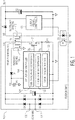
- Fig. 1 is a schematic block diagram of a flyback SMPS 100 in accordance with an embodiment of the invention.
- the flyback SMPS converts an input power to a desired output power (e.g., converts an input voltage level to a stable output voltage level for load currents within an acceptable range).
- the flyback SMPS delivers power available at an input of the flyback SMPS to a load in a controlled manner.
- the input power received at the flyback SMPS is Alternating Current (AC) power and the output power is an output voltage, such as a Direct Current (DC) voltage.
- the flyback SMPS can be used in various applications, such as automotive applications, communications applications, industrial applications, medical applications, computer applications, and/or consumer or appliance applications.
- the flyback SMPS may be included in a computing device, such as a smartphone, a tablet computer, a laptop, etc.
- the flyback converter is a buck-boost converter.
- the flyback SMPS 100 includes input terminals 102-1, 102-2, bridge rectifier diodes, "D1,” “D2,” “D3,” and “D4," an input capacitor, "C1,” a saturation controller 104, a metal-oxide-semiconductor field-effect transistor (MOSFET) switch, "S1,” a resistor, "R1,” a transformer, "T1,” a diode, “D5,” a capacitor, “Cvcc,” an output diode, “D6,” an output capacitor, “C2,” an output voltage controller 106, and an opto coupler, "O1.”
- the transformer, T1 includes an auxiliary winding 108, which is connected to a fixed voltage (e.g., the ground) via the diode, D5, and the capacitor, Cvcc, a primary winding 110, which is connected to the MOSFET switch, S1, and a second winding 112, which is connected to the diode, D
- the opto coupler, O1 may include a phototransistor, "P1,” and a diode, "D7.”
- the primary winding is connected to the drain terminal, "D,” of the MOSFET switch, S1
- the saturation controller is connected to the gate terminal, "G,” of the MOSFET switch, S1
- the resistor, R1 is connected to the source terminal, "S,” of the MOSFET switch, S1.
- at least one of the saturation controller and the output voltage controller is implemented on a substrate, such as a semiconductor wafer or a printed circuit board (PCB).
- at least one of the saturation controller and the output voltage controller is packaged as a stand-alone semiconductor Integrated Circuit (IC) chip.
- IC Integrated Circuit
- the flyback SMPS is shown in Fig. 1 as including certain circuit elements, in other embodiments, the flyback SMPS may include one or more additional/different circuit elements.
- the flyback SMPS is shown in Fig. 1 as including the MOSFET switch, S1, in other embodiments, the flyback SMPS may include other type of switches.
- the input terminals 102-1, 102-2 of the flyback SMPS 100 are connected to AC mains, which supply AC power to the input capacitor C1 through the bridge rectifier diodes, D1, D2, D3 and D4.
- the received energy is transferred to the output capacitor, C2, via the transformer, T1, and the rectifier diode, D6.
- the output voltage of the flyback SMPS is controlled by the output voltage controller 106 via the opto coupler, O1.
- the saturation controller 104 which is powered by the auxiliary winding 108 of the transformer, T1, via the rectifier diode, D5, drives the MOSFET switch, S1, to perform saturation control.
- the output voltage, Vout, of the flyback SMPS is low and the speed at which the current decreases in the output diode, D6, is slow.
- the transformer, T1 may saturate. For example, after a first switching period, if not all the energy from the transformer, T1, is transferred to the output capacitor, C2, the current in the diode, D6, will not have dropped to zero yet at the start of the next switching cycle, which will cause the current in the primary winding 110 to start from a non-zero value and the peak current in the transformer, T1, will increase over a voltage threshold, VL.
- VL voltage threshold
- a saturation controller can detect and control transformer saturation or demagnetisation of the flyback transformer, T1, by sensing the zero-voltage crossing on the auxiliary winding 108.
- an additional pin or electrical terminal is required in the saturation controller (e.g., a microcontroller IC) for the signal connection between the saturation controller and the auxiliary winding.
- the number of pins in an IC, especially a control IC is limited. In some instances, it can be expensive or even impossible to add a new pin to an existing controller IC.
- the saturation controller 104 is configured to reduce the saturation of the transformer, T1, without the need of an additional pin or electrical terminal.
- the saturation controller 104 depicted in Fig. 1 detects and controls the transformer saturation of the flyback transformer, T1, based on the length of primary strokes in the flyback SMPS 100.
- the saturation controller 104 can measure a length related to a primary stroke in the flyback SMPS 100, compare the length related to the primary stroke to a length related to a previous primary stroke in the flyback SMPS to generate a comparison result and adjust a switching period time of the flyback SMPS based on the comparison result such that saturation of the flyback SMPS is reduced.
- the saturation controller 104 is implemented as an IC (e.g., an IC chip) and the transformer, T1, is separate from the IC in which the saturation controller 104 is implemented. Consequently, the saturation controller 104 depicted in Fig. 1 does not require an extra pin for the sensed signal from the auxiliary winding 108. The lower number of pins typically allows a cheaper IC package. In addition, the chip area of the saturation controller 104 can be reduced because no bond pad with Electrostatic discharge (ESD) protection and connected circuitry is needed. Further, the saturation controller 104 depicted in Fig. 1 can be implemented with (i.e., compatible) with existing microcontroller ICs that have predetermined number of pins.
- ESD Electrostatic discharge
- the saturation controller 104 includes a stroke length detector 120, a stroke length comparator 122 and a switching period controller 124.
- each switching cycle or period of the flyback SMPS 100 includes a primary stroke and a secondary stroke.
- the MOSFET switch, S1 In the primary stroke of a switching period, the MOSFET switch, S1, is closed (connected) and energy from the AC mains is transferred to the transformer, T1.
- the MOSFET switch, S1 is opened (disconnected) and the energy stored in the transformer, T1, is discharged.
- the MOSFET switch, S1 In a continuous conduction mode, the MOSFET switch, S1, is controlled such that a primary stroke of the next switching cycle commences before the energy in the transformer, T1, falls to zero during the secondary stroke. In a discontinuous conduction mode, in which the MOSFET switch, S1, is controlled such that a primary stroke of the next switching cycle commences after a delay period has elapsed after the end of the secondary stroke.
- the stroke length detector is configured to measure a length related to a primary stroke in the flyback SMPS 100.
- the stroke length comparator is configured to compare the length related to the primary stroke to a length related to a previous primary stroke in the flyback SMPS to generate a comparison result.
- the switching period controller is configured to adjust a switching period time of the flyback SMPS based on the comparison result such that saturation of the flyback SMPS is reduced.
- the switching period controller 124 is further configured to extend the switching period time of the flyback SMPS if the length related to the primary stroke is shorter than the length related to the previous primary stroke and to reduce the switching period time of the flyback SMPS if the length related to the primary stroke is longer than or equal to the length related to the previous primary stroke.
- the switching period controller is further configured to adjust the signal, S G , at the gate terminal, G, of the MOSFET switch, S1, based on the comparison result, a second signal at the MOSFET switch, S1, and/or a third signal from the opto coupler, O1, of the flyback SMPS.
- Fig. 2 depicts an embodiment of the saturation controller 104 of the flyback SMPS 100 depicted in Fig. 1 .
- a saturation controller 204 includes a pulse width detector 220, a pulse width comparator 222, a switching period controller 224, and pulse width registers, "Reg1," "Reg2.”
- the switching period controller includes a delay element 230, a register 232, a first timer 234, a flip-flop circuit 236, a second timer 238, a comparator 240, an AND logic 242, and a power regulator 244.
- the saturation controller depicted in Fig. 2 is a possible implementation of the saturation controller depicted in Fig. 1 .
- the pulse width detector, the pulse width comparator and the switching period controller depicted in Fig. 2 are embodiments of the stroke length detector 120, the stroke length comparator 122 and the switching period controller 124 depicted in Fig. 1 , respectively.
- the saturation controller depicted in Fig. 1 can be implemented differently from the saturation controller depicted in Fig. 2 .
- the pulse width detector 220 is configured to measure a signal pulse width of the signal, S G , at the gate terminal, G, of the MOSFET switch, S1, that is connected to the primary winding 110 of the transformer, T1, of the flyback SMPS 100.
- the pulse width comparator 222 is configured to compare the signal pulse width of the signal, S G , (during the current switching period) with a previous signal pulse width of the signal, S G , (during the previous switching period) to generate a comparison result.
- the switching period controller 224 is configured to adjust a switching period time of the flyback SMPS based on the comparison result such that saturation of the flyback SMPS is reduced.
- the switching period controller is further configured to extend the switching period time of the flyback SMPS if the length related to the primary stroke is shorter than the length related to the previous primary stroke and to reduce the switching period time of the flyback SMPS if the length related to the primary stroke is longer than or equal to the length related to the previous primary stroke.
- the switching period controller may adjust the signal, S G , at the gate terminal, G, of the MOSFET switch, S1, based on the comparison result, a second signal at the MOSFET switch, S1, (e.g., the voltage signal, V s , at the source terminal, S, of the MOSFET switch, S1), and/or a third signal from the opto coupler, O1, of the flyback SMPS.
- FIG. 2 An example operation of the saturation controller 204 depicted in Fig. 2 is described as follows.
- T1 the timing of the signal, "S G ,” at the gate terminal, G, of the MOSFET switch, S1 is used for transformer saturation control.
- the signal, S G , at the gate terminal, G, of the MOSFET switch, S1 becomes logic high when the first timer 234 sets the flip-flop circuit 236.
- the gate signal, S G is reset after the blanking time when the sense voltage, "V s ,” (i.e., the voltage at the source terminal, S, of the MOSFET switch, S1, that is connected to the primary winding 110 of the transformer, T1), rises above the voltage threshold, VL, at an input of the comparator 240.
- the pulse width detector 220 measures the pulse width of the gate signal, S g , at the gate terminal, G, of the MOSFET switch, S1.
- the stored pulse width is transferred to the second pulse width register, Reg2, at the start of the next switching cycle, when the gate signal, S G , becomes logic high.
- the pulse width comparator 222 compares two pulse widths, "Ton0," and, "Ton1,” and outputs the comparison results to the register 232, which adjusts its value up or down based on the input signal.
- the stored value in the register 232 is updated with a short delay from the delay element 230 after the gate signal, S G , becomes logic low.
- the delay element is required because the output value of the register, Reg1, is also updated when the gate signal, S G , becomes logic low. The small delay generated by the delay element allows the output of the pulse width comparator to settle.
- the register, 232 outputs a delayed value, "dly,” which is used to control the first timer 234, which is triggered on the rising edge of the gate signal, S G . After a delay set by the input signal, dly, the output of the first timer 234 becomes logic high and starts a new switching cycle.
- the voltage threshold, VL is set by the power regulator 244, which receives its input from the opto coupler, O1 (shown in Fig. 1 ).
- the output power of the flyback SMPS 100 is regulated by the power regulator by adjusting the voltage threshold, VL. Specifically, to increase the output power of the flyback SMPS, the voltage threshold, VL, is increased, and to reduce the output power, the voltage threshold, VL, is reduced.
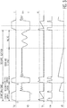
- Fig. 3 is a signal timing diagram corresponding to the flyback SMPS 100 depicted in Fig. 1 with the saturation controller 204 depicted in Fig. 2 .
- the signals illustrated in Fig. 3 include the signal, S G , at the gate terminal, G, of the MOSFET switch, S1, the drain voltage, V D , at the drain terminal, D, of the MOSFET switch, S1, the sense voltage, V s , the comparison result, I pk , from the comparator 240, and the current, Id6, in the output diode, D6.
- the switching sequence is drawn for multiple switching cycles. If a shorter primary stroke is detected (for the same voltage threshold, VL), the start of the next primary stroke is delayed, allowing the current, Id6, in the output diode, D6, to drop to zero again.
- a primary stroke (referred to as the first primary stroke) of a first switching period starts, while at time point, t2, a primary stroke (referred to as the second primary stroke) of a second switching period starts.
- the length of a primary stroke may be detected by measuring the time duration between time point, t0, in which the signal, S G , rises and time point, t1, in which the signal, V D , rises.
- the length of the second primary stroke is shorter than the length of the first primary stroke, and the switching period is increased, which allows the current, Id6, in the output diode, D6, to drop to zero.
- the switching period is increased enough to guarantee the discontinuous operation.
- a ringing period appears.
- the ringing period reflects the free oscillation of the capacitance of the drain terminal, D, of the MOSFET switch, S1, and the primary transformer winding inductance.
- the flyback SMPS 100 is not active during the ringing period and no energy is built up in the transformer, T1, or released to the secondary side.
- the switching period can be reduced in small steps until the length of the primary stroke is shorter than the length of a previous primary stroke.
- the switching period is again increased with a larger step.
- This operation of decreasing the switching period by a smaller step and increasing the switching period by a larger step, resulting in an operation mode which is mostly in discontinuous conduction mode (DCM), and only single switching cycles in continuous conduction mode (CCM).
- DCM discontinuous conduction mode
- CCM continuous conduction mode
- the flyback SMPS operates under DCM mostly.
- the flyback SMPS may operate under CCM if the switching period is reduced to 10 microseconds ( ⁇ s). If the switching period is reduced from 20 ⁇ s by 1 ⁇ s each switching cycle, after 10 switching cycles, the flyback SMPS starts to operate under CCM.
- the flyback SMPS may operate under DCM for the next 5 switching cycles even if the switching period is reduced by 1 ⁇ s each switching cycle.
- the flyback SMPS operates 1 switching cycle under CCM and 5 switching cycles under DCM. Consequently, there is no current run-away and the transformer is not saturated in this operation mode.
- the switching period is changed in certain manner in Fig. 3 , in other embodiments, the switching period may be changed in different manners. For example, smaller/larger steps may be used and the ringing period may be minimized to reduce the non-active time of the flyback SMPS.
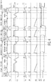
- Fig. 4 is another signal timing diagram corresponding to the flyback SMPS 100 depicted in Fig. 1 with the saturation controller 204 depicted in Fig. 2 .
- the signals illustrated in Fig. 4 include the signal, S G , at the gate terminal, G, of the MOSFET switch, S1, the drain voltage, V D , at the drain terminal, D, of the MOSFET switch, S1, the sense voltage, V s , the comparison result, I pk , from the comparator 240, and the current, Id6, in the output diode, D6, pulse widths, TonO, Ton1, from the pulse width registers, Reg1, Reg2, and the delayed value, dly, from the register, 232.
- the switching sequence is drawn for multiple switching cycles.
- the flyback SMPS 100 is in discontinuous conduction mode.
- the current, Id6, in the output diode, D6, drops to zero before the next switching cycle/period is started.
- the flyback SMPS is not active during the ringing period and no energy is built up in the transformer, T1, or released to the secondary side. Because the flyback SMPS is not active, the flyback SMPS cannot output the maximum output power and the transformer, T1, is not used to its full potential, which is unwanted because that would require a larger transformer than needed.
- the switching period is reduced and the ringing time is reduced, which increases the output power.
- the length of the primary stroke is equal to the length of the first and second primary strokes and the flyback SMPS is still in discontinuous conduction mode.
- the current at the primary stroke starts from zero, at time point t4.
- the third switching period is reduced even further, which results in a situation where not all the energy is transferred to the secondary side.
- the current, Id6, in the diode, d6, has not dropped to zero before the fourth primary stroke has started, at time point t5.
- the sense voltage, V s also does not start from zero, which results in the sense voltage, V s , reaching the voltage threshold, VL, shortly after the switching cycle starts.
- the pulse widths, Ton0, Ton1, from the pulse width registers, Reg1, Reg2, are identical to each other in the first, second and third switching periods.
- the primary stroke is shorter than previous primary strokes and specifically, at time point, t6, the pulse width, Ton0, is narrower/lower than the pulse width, Ton1. Consequently, the saturation controller 204 extends the fourth switching period. Then for the next switching cycle (i.e., the fifth switching period), the flyback SMPS is operating in discontinuous conduction mode again.
- the switching period is changed in certain manner in Fig. 4 , in other embodiments, the switching period may be changed in different manners. For example, smaller/larger steps may be used and the ringing period may be minimized to reduce the non-active time of the flyback SMPS.
- Fig. 5 depicts four operational stages 510, 520, 530, 540 of the saturation controller 204 depicted in Fig. 2 .
- a large switching period is set for discontinuous conduction mode.
- the initial stored value for the primary stroke is short (can be zero).
- the second operational stage 520 the first switching cycle/period is started and when the peak value of the comparison result, Ipk, is reached, the length of the primary stroke is compared to the length of the previous primary stroke. For the first switching cycle, the length of the primary stroke is longer than the initial value.
- the switching period is reduced with a small step for the next switching cycle.
- the length of the primary stroke is compared again to the length of the primary stroke of the previous switching cycle. If the length of the primary stroke is still longer than or equal to the length of the previous primary stroke, the switching period is reduced further in the fourth operational stage 540. If the length of the primary stroke is shorter than the length of the previous primary stroke, continuous conduction mode operation is assumed and for the next switching cycle the switching period time is extended in the third operational stage 530. In some embodiments, the step for switching period extension is larger than the step for switching period reduction. The operation of reducing and increasing the switching period continues, resulting in an operation mode with only single switching cycles in continuous conduction mode followed by multiple switching cycles is discontinuous conduction mode. Because there are only single cycles in continuous conduction mode, there is no chance for current run-away and transformer saturation. The flyback SMPS 100 can be used to its maximum power while saturation is avoided.
- Fig. 6 is a schematic block diagram of a flyback SMPS 600 in accordance with another embodiment of the invention.
- a difference between the flyback SMPS 600 depicted in Fig. 6 and the flyback SMPS 100 depicted in Fig. 1 is that a transformer, T6, of the flyback SMPS 600 depicted in Fig. 6 does not include an auxiliary winding (e.g., the auxiliary winding 108 included in the transformer, T1, of the flyback SMPS 100 depicted in Fig. 1 ).
- auxiliary winding e.g., the auxiliary winding 108 included in the transformer, T1, of the flyback SMPS 100 depicted in Fig. 1 .
- the flyback SMPS includes input terminals 602-1, 602-2, the bridge rectifier diodes, D1, D2, D3, and D4, the input capacitor, C1, the saturation controller 104, the MOSFET switch, S1, resistors, R1, R1, the capacitor, Cvcc, a second resistor, "R2," the transformer, T6, the output diode, D6, the output capacitor, C2, the output voltage controller 106, and the opto coupler, O1.
- the transformer, T6, includes a primary winding 610, which is connected to the MOSFET switch, S1, and the saturation controller via the resistor, R2, and a second winding 612, which is connected to the diode, D6, the output voltage controller and the output capacitor, C2.
- the supply voltage, Vcc, for the saturation controller is from the rectified mains voltage, Vin, via the resistor, R2.
- at least one of the saturation controller and the output voltage controller is implemented on a substrate, such as a semiconductor wafer or a printed circuit board (PCB).
- at least one of the saturation controller and the output voltage controller is packaged as a stand-alone semiconductor IC chip.
- the flyback SMPS is shown in Fig. 6 as including certain circuit elements, in other embodiments, the flyback SMPS may include one or more additional circuit elements.
- the operation of the flyback SMPS 600 depicted in Fig. 6 is similar to the operation of the flyback SMPS 100 depicted in Fig. 1 .
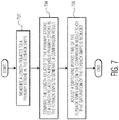
- Fig. 7 is a process flow diagram of a method for saturation control for a flyback SMPS in accordance with an embodiment of the invention.
- a length related to a primary stroke in the flyback SMPS is measured.
- the length related to the primary stroke is compared to a length related to a previous primary stroke in the flyback SMPS to generate a comparison result.
- a switching period time of the flyback SMPS is adjusted based on the comparison result such that saturation of the flyback SMPS is reduced.
- the flyback SMPS may be the same as or similar to the flyback SMPS 100 depicted in Fig. 1 and/or the flyback SMPS 600 depicted in Fig. 3 .
- an embodiment of a computer program product includes a computer useable storage medium to store a computer readable program.
- the computer-useable or computer-readable storage medium can be an electronic, magnetic, optical, electromagnetic, infrared, or semiconductor system (or apparatus or device).
- Examples of non-transitory computer-useable and computer-readable storage media include a semiconductor or solid state memory, magnetic tape, a removable computer diskette, a random access memory (RAM), a read-only memory (ROM), a rigid magnetic disk, and an optical disk.
- Current examples of optical disks include a compact disk with read only memory (CD-ROM), a compact disk with read/write (CD-R/W), and a digital video disk (DVD).
- embodiments of the invention may be implemented entirely in hardware or in an implementation containing both hardware and software elements.
- the software may include but is not limited to firmware, resident software, microcode, etc.
Landscapes
- Engineering & Computer Science (AREA)
- Power Engineering (AREA)
- Dc-Dc Converters (AREA)
Applications Claiming Priority (1)
| Application Number | Priority Date | Filing Date | Title |
|---|---|---|---|
| US15/956,649 US10158296B1 (en) | 2018-04-18 | 2018-04-18 | Method and system for saturation control in a flyback switched-mode power supply (SMPS) |
Publications (2)
| Publication Number | Publication Date |
|---|---|
| EP3562018A1 true EP3562018A1 (de) | 2019-10-30 |
| EP3562018B1 EP3562018B1 (de) | 2020-10-28 |
Family
ID=64604947
Family Applications (1)
| Application Number | Title | Priority Date | Filing Date |
|---|---|---|---|
| EP19165117.3A Active EP3562018B1 (de) | 2018-04-18 | 2019-03-26 | Verfahren und system zur sättigungssteuerung in einem flyback-schaltnetzteil (smps) |
Country Status (3)
| Country | Link |
|---|---|
| US (1) | US10158296B1 (de) |
| EP (1) | EP3562018B1 (de) |
| CN (1) | CN110391750B (de) |
Families Citing this family (1)
| Publication number | Priority date | Publication date | Assignee | Title |
|---|---|---|---|---|
| US10895601B2 (en) * | 2019-05-10 | 2021-01-19 | Infineon Technologies Ag | System and method of monitoring a switching transistor |
Citations (1)
| Publication number | Priority date | Publication date | Assignee | Title |
|---|---|---|---|---|
| WO2012088505A1 (en) * | 2010-12-23 | 2012-06-28 | Marvell World Trade Ltd | Reducing voltage stress in a flyback converter design |
Family Cites Families (30)
| Publication number | Priority date | Publication date | Assignee | Title |
|---|---|---|---|---|
| NL8900509A (nl) | 1989-03-02 | 1990-10-01 | Philips Nv | Geschakelde voedingsspanningsschakeling. |
| ES2051950T3 (es) | 1989-09-29 | 1994-07-01 | Siemens Ag | Disposicion de circuito para una fuente de alimentacion de conexion de transformador de bloqueo. |
| DE4001324A1 (de) | 1990-01-18 | 1991-07-25 | Philips Patentverwaltung | Gleichspannungssperrwandler |
| AT406319B (de) * | 1995-10-24 | 2000-04-25 | Siemens Ag Oesterreich | Sperrwandler |
| US6219493B1 (en) * | 1998-08-19 | 2001-04-17 | Konica Corporation | Electronic flash device of a separate excitation oscillating type |
| EP1001513B1 (de) * | 1998-11-16 | 2009-06-03 | Alcatel Lucent | Universeller Schaltstromwandler |
| JP2000324683A (ja) | 1999-05-06 | 2000-11-24 | Matsushita Electric Ind Co Ltd | 保護回路 |
| US6487097B2 (en) | 2000-03-16 | 2002-11-26 | Altel Technology | Feedforward clamping applied to the control voltage in switch mode power supplies (SMPS) |
| JP3707409B2 (ja) | 2001-09-10 | 2005-10-19 | 株式会社村田製作所 | スイッチング電源装置 |
| JP3707436B2 (ja) | 2002-01-25 | 2005-10-19 | 株式会社村田製作所 | スイッチング電源装置 |
| JP4148760B2 (ja) * | 2002-11-13 | 2008-09-10 | 新電元工業株式会社 | スイッチング電源装置 |
| US6768657B1 (en) * | 2003-03-19 | 2004-07-27 | System General Corp. | Current-driven PWM controller having a power saving means |
| US6836415B1 (en) * | 2003-06-18 | 2004-12-28 | Systems General Corp. | Primary-side regulated pulse width modulation controller with improved load regulation |
| WO2005101624A1 (en) * | 2004-04-13 | 2005-10-27 | System General Corp. | Pwm controller having a modulator for saving power and reducing acoustic noise |
| US7589983B1 (en) * | 2005-11-10 | 2009-09-15 | Iwatt Inc. | Power converter controller controlled by variable reference voltage generated by dual output digital to analog converter |
| US7724547B1 (en) * | 2006-09-15 | 2010-05-25 | Iwatt Inc. | Compensating on-time delay of switching transistor in switching power converters |
| US7554473B2 (en) | 2007-05-02 | 2009-06-30 | Cirrus Logic, Inc. | Control system using a nonlinear delta-sigma modulator with nonlinear process modeling |
| GB2460266A (en) * | 2008-05-23 | 2009-11-25 | Cambridge Semiconductor Ltd | Estimating conduction times of a switch mode power supply transformer |
| CN101686014B (zh) * | 2008-09-24 | 2012-11-28 | 通嘉科技股份有限公司 | 返驰式交换电源供应器及其控制方法 |
| TWI379496B (en) * | 2010-04-02 | 2012-12-11 | Macroblock Inc | Isolated primary side regulator |
| CN102364859B (zh) | 2011-05-31 | 2014-11-26 | 杭州士兰微电子股份有限公司 | 开关电源控制装置及包含该控制装置的反激式开关电源 |
| EP2557674B1 (de) * | 2011-08-11 | 2018-11-14 | Nxp B.V. | Schaltung für ein Schaltnetzteil |
| WO2013080403A1 (ja) * | 2011-11-28 | 2013-06-06 | パナソニック株式会社 | スイッチング電源装置および半導体装置 |
| US9602006B2 (en) * | 2012-10-24 | 2017-03-21 | Infineon Technologies Ag | Method and a controller for determining a demagnetization zero current time for a switched mode power supply |
| US9564817B2 (en) * | 2014-03-17 | 2017-02-07 | Semiconductor Components Industries, Llc | Method and apparatus for dedicated skip mode for resonant converters |
| TWI568159B (zh) * | 2014-04-24 | 2017-01-21 | 立錡科技股份有限公司 | 返馳式電源供應器及其控制電路與控制方法 |
| JP2016059138A (ja) * | 2014-09-08 | 2016-04-21 | シャープ株式会社 | スイッチング電源装置 |
| WO2016076121A1 (ja) * | 2014-11-12 | 2016-05-19 | 株式会社村田製作所 | 電源モジュールおよびその実装構造 |
| CN104617792B (zh) * | 2014-12-24 | 2017-12-15 | 昂宝电子(上海)有限公司 | 用于初级侧调节的电源变换系统的电压调节的系统和方法 |
| US10522306B2 (en) * | 2016-05-27 | 2019-12-31 | North Carolina State University | System and method of causing a zero-current crossing in an electrical circuit |
-
2018
- 2018-04-18 US US15/956,649 patent/US10158296B1/en active Active
-
2019
- 2019-03-26 EP EP19165117.3A patent/EP3562018B1/de active Active
- 2019-04-18 CN CN201910315850.3A patent/CN110391750B/zh active Active
Patent Citations (1)
| Publication number | Priority date | Publication date | Assignee | Title |
|---|---|---|---|---|
| WO2012088505A1 (en) * | 2010-12-23 | 2012-06-28 | Marvell World Trade Ltd | Reducing voltage stress in a flyback converter design |
Non-Patent Citations (1)
| Title |
|---|
| ADRAGNA C: "L6565 Quasi-Resonant Controller", INTERNET CITATION, 1 November 2002 (2002-11-01), XP002407906, Retrieved from the Internet <URL:http://www.st.com/stonline/products/literature/an/7578.pdf> [retrieved on 10771101] * |
Also Published As
| Publication number | Publication date |
|---|---|
| EP3562018B1 (de) | 2020-10-28 |
| CN110391750A (zh) | 2019-10-29 |
| CN110391750B (zh) | 2024-01-09 |
| US10158296B1 (en) | 2018-12-18 |
Similar Documents
| Publication | Publication Date | Title |
|---|---|---|
| US9479067B2 (en) | System and method for a switched-mode power supply | |
| US9231483B2 (en) | DC/DC converter | |
| US8749994B2 (en) | Switched-mode power supply | |
| CN102273057B (zh) | 用于切换功率转换器的谷模式切换方案 | |
| US7592790B2 (en) | Start-up circuit with feedforward compensation for power converters | |
| US9948187B2 (en) | System and method for a switched-mode power supply | |
| US20110002068A1 (en) | Switching regulator with fault protection and method thereof | |
| US20110122659A1 (en) | Power transistor driving circuits and methods for switching mode power supplies | |
| US20160190942A1 (en) | Insulated synchronous rectification dc/dc converter | |
| TW202226724A (zh) | 返馳變換器電源及其控制方法 | |
| US9318961B2 (en) | Switching power-supply device | |
| US9742299B2 (en) | Insulated synchronous rectification DC/DC converter | |
| CN108173434A (zh) | 开关电源电路 | |
| US8964412B2 (en) | Split current mirror line sensing | |
| CN104795997A (zh) | 正向转换器及次级侧开关控制器 | |
| TWI649948B (zh) | 具有主動式突波吸收器的控制模組及相關的返馳式電源轉換裝置 | |
| JP7421075B2 (ja) | スイッチング電源用半導体装置並びにスイッチング電源装置 | |
| US20140160803A1 (en) | Dc/dc converter | |
| TW201933739A (zh) | 具限功率電源保護功能的返馳式開關電源 | |
| TW202127783A (zh) | 電源轉換系統 | |
| CN207098932U (zh) | 一种开关电源控制电路、开关电源电路 | |
| US20240322699A1 (en) | Synchronous Rectifier Scheme to Avoid Cross-conduction in a Fly-Back Converter | |
| EP3562018B1 (de) | Verfahren und system zur sättigungssteuerung in einem flyback-schaltnetzteil (smps) | |
| CN116111819A (zh) | Acf变换器中的逐周期反向电流限制 | |
| CN115693590A (zh) | 电流采样电阻短路保护电路、方法、芯片、系统及设备 |
Legal Events
| Date | Code | Title | Description |
|---|---|---|---|
| PUAI | Public reference made under article 153(3) epc to a published international application that has entered the european phase |
Free format text: ORIGINAL CODE: 0009012 |
|
| STAA | Information on the status of an ep patent application or granted ep patent |
Free format text: STATUS: THE APPLICATION HAS BEEN PUBLISHED |
|
| AK | Designated contracting states |
Kind code of ref document: A1 Designated state(s): AL AT BE BG CH CY CZ DE DK EE ES FI FR GB GR HR HU IE IS IT LI LT LU LV MC MK MT NL NO PL PT RO RS SE SI SK SM TR |
|
| AX | Request for extension of the european patent |
Extension state: BA ME |
|
| STAA | Information on the status of an ep patent application or granted ep patent |
Free format text: STATUS: REQUEST FOR EXAMINATION WAS MADE |
|
| 17P | Request for examination filed |
Effective date: 20200430 |
|
| RBV | Designated contracting states (corrected) |
Designated state(s): AL AT BE BG CH CY CZ DE DK EE ES FI FR GB GR HR HU IE IS IT LI LT LU LV MC MK MT NL NO PL PT RO RS SE SI SK SM TR |
|
| GRAP | Despatch of communication of intention to grant a patent |
Free format text: ORIGINAL CODE: EPIDOSNIGR1 |
|
| STAA | Information on the status of an ep patent application or granted ep patent |
Free format text: STATUS: GRANT OF PATENT IS INTENDED |
|
| RIC1 | Information provided on ipc code assigned before grant |
Ipc: H02M 1/40 20070101ALI20200514BHEP Ipc: H02M 3/335 20060101AFI20200514BHEP |
|
| INTG | Intention to grant announced |
Effective date: 20200612 |
|
| GRAS | Grant fee paid |
Free format text: ORIGINAL CODE: EPIDOSNIGR3 |
|
| GRAA | (expected) grant |
Free format text: ORIGINAL CODE: 0009210 |
|
| STAA | Information on the status of an ep patent application or granted ep patent |
Free format text: STATUS: THE PATENT HAS BEEN GRANTED |
|
| AK | Designated contracting states |
Kind code of ref document: B1 Designated state(s): AL AT BE BG CH CY CZ DE DK EE ES FI FR GB GR HR HU IE IS IT LI LT LU LV MC MK MT NL NO PL PT RO RS SE SI SK SM TR |
|
| REG | Reference to a national code |
Ref country code: GB Ref legal event code: FG4D |
|
| REG | Reference to a national code |
Ref country code: CH Ref legal event code: EP |
|
| REG | Reference to a national code |
Ref country code: AT Ref legal event code: REF Ref document number: 1329239 Country of ref document: AT Kind code of ref document: T Effective date: 20201115 |
|
| REG | Reference to a national code |
Ref country code: DE Ref legal event code: R096 Ref document number: 602019001078 Country of ref document: DE |
|
| REG | Reference to a national code |
Ref country code: IE Ref legal event code: FG4D |
|
| REG | Reference to a national code |
Ref country code: AT Ref legal event code: MK05 Ref document number: 1329239 Country of ref document: AT Kind code of ref document: T Effective date: 20201028 |
|
| REG | Reference to a national code |
Ref country code: NL Ref legal event code: MP Effective date: 20201028 |
|
| PG25 | Lapsed in a contracting state [announced via postgrant information from national office to epo] |
Ref country code: FI Free format text: LAPSE BECAUSE OF FAILURE TO SUBMIT A TRANSLATION OF THE DESCRIPTION OR TO PAY THE FEE WITHIN THE PRESCRIBED TIME-LIMIT Effective date: 20201028 Ref country code: PT Free format text: LAPSE BECAUSE OF FAILURE TO SUBMIT A TRANSLATION OF THE DESCRIPTION OR TO PAY THE FEE WITHIN THE PRESCRIBED TIME-LIMIT Effective date: 20210301 Ref country code: RS Free format text: LAPSE BECAUSE OF FAILURE TO SUBMIT A TRANSLATION OF THE DESCRIPTION OR TO PAY THE FEE WITHIN THE PRESCRIBED TIME-LIMIT Effective date: 20201028 Ref country code: GR Free format text: LAPSE BECAUSE OF FAILURE TO SUBMIT A TRANSLATION OF THE DESCRIPTION OR TO PAY THE FEE WITHIN THE PRESCRIBED TIME-LIMIT Effective date: 20210129 Ref country code: NO Free format text: LAPSE BECAUSE OF FAILURE TO SUBMIT A TRANSLATION OF THE DESCRIPTION OR TO PAY THE FEE WITHIN THE PRESCRIBED TIME-LIMIT Effective date: 20210128 |
|
| REG | Reference to a national code |
Ref country code: LT Ref legal event code: MG4D |
|
| PG25 | Lapsed in a contracting state [announced via postgrant information from national office to epo] |
Ref country code: SE Free format text: LAPSE BECAUSE OF FAILURE TO SUBMIT A TRANSLATION OF THE DESCRIPTION OR TO PAY THE FEE WITHIN THE PRESCRIBED TIME-LIMIT Effective date: 20201028 Ref country code: PL Free format text: LAPSE BECAUSE OF FAILURE TO SUBMIT A TRANSLATION OF THE DESCRIPTION OR TO PAY THE FEE WITHIN THE PRESCRIBED TIME-LIMIT Effective date: 20201028 Ref country code: LV Free format text: LAPSE BECAUSE OF FAILURE TO SUBMIT A TRANSLATION OF THE DESCRIPTION OR TO PAY THE FEE WITHIN THE PRESCRIBED TIME-LIMIT Effective date: 20201028 Ref country code: IS Free format text: LAPSE BECAUSE OF FAILURE TO SUBMIT A TRANSLATION OF THE DESCRIPTION OR TO PAY THE FEE WITHIN THE PRESCRIBED TIME-LIMIT Effective date: 20210228 Ref country code: BG Free format text: LAPSE BECAUSE OF FAILURE TO SUBMIT A TRANSLATION OF THE DESCRIPTION OR TO PAY THE FEE WITHIN THE PRESCRIBED TIME-LIMIT Effective date: 20210128 Ref country code: ES Free format text: LAPSE BECAUSE OF FAILURE TO SUBMIT A TRANSLATION OF THE DESCRIPTION OR TO PAY THE FEE WITHIN THE PRESCRIBED TIME-LIMIT Effective date: 20201028 Ref country code: AT Free format text: LAPSE BECAUSE OF FAILURE TO SUBMIT A TRANSLATION OF THE DESCRIPTION OR TO PAY THE FEE WITHIN THE PRESCRIBED TIME-LIMIT Effective date: 20201028 |
|
| PG25 | Lapsed in a contracting state [announced via postgrant information from national office to epo] |
Ref country code: HR Free format text: LAPSE BECAUSE OF FAILURE TO SUBMIT A TRANSLATION OF THE DESCRIPTION OR TO PAY THE FEE WITHIN THE PRESCRIBED TIME-LIMIT Effective date: 20201028 Ref country code: NL Free format text: LAPSE BECAUSE OF FAILURE TO SUBMIT A TRANSLATION OF THE DESCRIPTION OR TO PAY THE FEE WITHIN THE PRESCRIBED TIME-LIMIT Effective date: 20201028 |
|
| REG | Reference to a national code |
Ref country code: DE Ref legal event code: R097 Ref document number: 602019001078 Country of ref document: DE |
|
| PG25 | Lapsed in a contracting state [announced via postgrant information from national office to epo] |
Ref country code: RO Free format text: LAPSE BECAUSE OF FAILURE TO SUBMIT A TRANSLATION OF THE DESCRIPTION OR TO PAY THE FEE WITHIN THE PRESCRIBED TIME-LIMIT Effective date: 20201028 Ref country code: LT Free format text: LAPSE BECAUSE OF FAILURE TO SUBMIT A TRANSLATION OF THE DESCRIPTION OR TO PAY THE FEE WITHIN THE PRESCRIBED TIME-LIMIT Effective date: 20201028 Ref country code: SK Free format text: LAPSE BECAUSE OF FAILURE TO SUBMIT A TRANSLATION OF THE DESCRIPTION OR TO PAY THE FEE WITHIN THE PRESCRIBED TIME-LIMIT Effective date: 20201028 Ref country code: SM Free format text: LAPSE BECAUSE OF FAILURE TO SUBMIT A TRANSLATION OF THE DESCRIPTION OR TO PAY THE FEE WITHIN THE PRESCRIBED TIME-LIMIT Effective date: 20201028 Ref country code: EE Free format text: LAPSE BECAUSE OF FAILURE TO SUBMIT A TRANSLATION OF THE DESCRIPTION OR TO PAY THE FEE WITHIN THE PRESCRIBED TIME-LIMIT Effective date: 20201028 Ref country code: CZ Free format text: LAPSE BECAUSE OF FAILURE TO SUBMIT A TRANSLATION OF THE DESCRIPTION OR TO PAY THE FEE WITHIN THE PRESCRIBED TIME-LIMIT Effective date: 20201028 |
|
| PG25 | Lapsed in a contracting state [announced via postgrant information from national office to epo] |
Ref country code: DK Free format text: LAPSE BECAUSE OF FAILURE TO SUBMIT A TRANSLATION OF THE DESCRIPTION OR TO PAY THE FEE WITHIN THE PRESCRIBED TIME-LIMIT Effective date: 20201028 |
|
| PLBE | No opposition filed within time limit |
Free format text: ORIGINAL CODE: 0009261 |
|
| STAA | Information on the status of an ep patent application or granted ep patent |
Free format text: STATUS: NO OPPOSITION FILED WITHIN TIME LIMIT |
|
| 26N | No opposition filed |
Effective date: 20210729 |
|
| PG25 | Lapsed in a contracting state [announced via postgrant information from national office to epo] |
Ref country code: IT Free format text: LAPSE BECAUSE OF FAILURE TO SUBMIT A TRANSLATION OF THE DESCRIPTION OR TO PAY THE FEE WITHIN THE PRESCRIBED TIME-LIMIT Effective date: 20201028 Ref country code: MC Free format text: LAPSE BECAUSE OF FAILURE TO SUBMIT A TRANSLATION OF THE DESCRIPTION OR TO PAY THE FEE WITHIN THE PRESCRIBED TIME-LIMIT Effective date: 20201028 Ref country code: AL Free format text: LAPSE BECAUSE OF FAILURE TO SUBMIT A TRANSLATION OF THE DESCRIPTION OR TO PAY THE FEE WITHIN THE PRESCRIBED TIME-LIMIT Effective date: 20201028 |
|
| PG25 | Lapsed in a contracting state [announced via postgrant information from national office to epo] |
Ref country code: SI Free format text: LAPSE BECAUSE OF FAILURE TO SUBMIT A TRANSLATION OF THE DESCRIPTION OR TO PAY THE FEE WITHIN THE PRESCRIBED TIME-LIMIT Effective date: 20201028 |
|
| REG | Reference to a national code |
Ref country code: BE Ref legal event code: MM Effective date: 20210331 |
|
| PG25 | Lapsed in a contracting state [announced via postgrant information from national office to epo] |
Ref country code: IE Free format text: LAPSE BECAUSE OF NON-PAYMENT OF DUE FEES Effective date: 20210326 Ref country code: FR Free format text: LAPSE BECAUSE OF NON-PAYMENT OF DUE FEES Effective date: 20210331 Ref country code: LU Free format text: LAPSE BECAUSE OF NON-PAYMENT OF DUE FEES Effective date: 20210326 |
|
| PG25 | Lapsed in a contracting state [announced via postgrant information from national office to epo] |
Ref country code: IS Free format text: LAPSE BECAUSE OF FAILURE TO SUBMIT A TRANSLATION OF THE DESCRIPTION OR TO PAY THE FEE WITHIN THE PRESCRIBED TIME-LIMIT Effective date: 20210228 |
|
| PG25 | Lapsed in a contracting state [announced via postgrant information from national office to epo] |
Ref country code: BE Free format text: LAPSE BECAUSE OF NON-PAYMENT OF DUE FEES Effective date: 20210331 |
|
| REG | Reference to a national code |
Ref country code: CH Ref legal event code: PL |
|
| PG25 | Lapsed in a contracting state [announced via postgrant information from national office to epo] |
Ref country code: LI Free format text: LAPSE BECAUSE OF NON-PAYMENT OF DUE FEES Effective date: 20220331 Ref country code: CH Free format text: LAPSE BECAUSE OF NON-PAYMENT OF DUE FEES Effective date: 20220331 |
|
| PG25 | Lapsed in a contracting state [announced via postgrant information from national office to epo] |
Ref country code: CY Free format text: LAPSE BECAUSE OF FAILURE TO SUBMIT A TRANSLATION OF THE DESCRIPTION OR TO PAY THE FEE WITHIN THE PRESCRIBED TIME-LIMIT Effective date: 20201028 |
|
| PG25 | Lapsed in a contracting state [announced via postgrant information from national office to epo] |
Ref country code: HU Free format text: LAPSE BECAUSE OF FAILURE TO SUBMIT A TRANSLATION OF THE DESCRIPTION OR TO PAY THE FEE WITHIN THE PRESCRIBED TIME-LIMIT; INVALID AB INITIO Effective date: 20190326 |
|
| P01 | Opt-out of the competence of the unified patent court (upc) registered |
Effective date: 20230725 |
|
| GBPC | Gb: european patent ceased through non-payment of renewal fee |
Effective date: 20230326 |
|
| PG25 | Lapsed in a contracting state [announced via postgrant information from national office to epo] |
Ref country code: GB Free format text: LAPSE BECAUSE OF NON-PAYMENT OF DUE FEES Effective date: 20230326 |
|
| PG25 | Lapsed in a contracting state [announced via postgrant information from national office to epo] |
Ref country code: GB Free format text: LAPSE BECAUSE OF NON-PAYMENT OF DUE FEES Effective date: 20230326 |
|
| PG25 | Lapsed in a contracting state [announced via postgrant information from national office to epo] |
Ref country code: MK Free format text: LAPSE BECAUSE OF FAILURE TO SUBMIT A TRANSLATION OF THE DESCRIPTION OR TO PAY THE FEE WITHIN THE PRESCRIBED TIME-LIMIT Effective date: 20201028 |
|
| PG25 | Lapsed in a contracting state [announced via postgrant information from national office to epo] |
Ref country code: MT Free format text: LAPSE BECAUSE OF FAILURE TO SUBMIT A TRANSLATION OF THE DESCRIPTION OR TO PAY THE FEE WITHIN THE PRESCRIBED TIME-LIMIT Effective date: 20201028 |
|
| PG25 | Lapsed in a contracting state [announced via postgrant information from national office to epo] |
Ref country code: TR Free format text: LAPSE BECAUSE OF FAILURE TO SUBMIT A TRANSLATION OF THE DESCRIPTION OR TO PAY THE FEE WITHIN THE PRESCRIBED TIME-LIMIT Effective date: 20201028 |
|
| PGFP | Annual fee paid to national office [announced via postgrant information from national office to epo] |
Ref country code: DE Payment date: 20260219 Year of fee payment: 8 |