EP3561884A1 - Lichtemittierende vorrichtung - Google Patents
Lichtemittierende vorrichtung Download PDFInfo
- Publication number
- EP3561884A1 EP3561884A1 EP19170592.0A EP19170592A EP3561884A1 EP 3561884 A1 EP3561884 A1 EP 3561884A1 EP 19170592 A EP19170592 A EP 19170592A EP 3561884 A1 EP3561884 A1 EP 3561884A1
- Authority
- EP
- European Patent Office
- Prior art keywords
- light
- insulating film
- contact surface
- type semiconductor
- semiconductor layer
- Prior art date
- Legal status (The legal status is an assumption and is not a legal conclusion. Google has not performed a legal analysis and makes no representation as to the accuracy of the status listed.)
- Pending
Links
Images



Classifications
-
- H—ELECTRICITY
- H10—SEMICONDUCTOR DEVICES; ELECTRIC SOLID-STATE DEVICES NOT OTHERWISE PROVIDED FOR
- H10H—INORGANIC LIGHT-EMITTING SEMICONDUCTOR DEVICES HAVING POTENTIAL BARRIERS
- H10H20/00—Individual inorganic light-emitting semiconductor devices having potential barriers, e.g. light-emitting diodes [LED]
- H10H20/80—Constructional details
- H10H20/84—Coatings, e.g. passivation layers or antireflective coatings
- H10H20/841—Reflective coatings, e.g. dielectric Bragg reflectors
-
- H—ELECTRICITY
- H10—SEMICONDUCTOR DEVICES; ELECTRIC SOLID-STATE DEVICES NOT OTHERWISE PROVIDED FOR
- H10H—INORGANIC LIGHT-EMITTING SEMICONDUCTOR DEVICES HAVING POTENTIAL BARRIERS
- H10H20/00—Individual inorganic light-emitting semiconductor devices having potential barriers, e.g. light-emitting diodes [LED]
- H10H20/80—Constructional details
- H10H20/83—Electrodes
- H10H20/831—Electrodes characterised by their shape
-
- H—ELECTRICITY
- H10—SEMICONDUCTOR DEVICES; ELECTRIC SOLID-STATE DEVICES NOT OTHERWISE PROVIDED FOR
- H10H—INORGANIC LIGHT-EMITTING SEMICONDUCTOR DEVICES HAVING POTENTIAL BARRIERS
- H10H20/00—Individual inorganic light-emitting semiconductor devices having potential barriers, e.g. light-emitting diodes [LED]
- H10H20/80—Constructional details
- H10H20/83—Electrodes
- H10H20/832—Electrodes characterised by their material
- H10H20/835—Reflective materials
-
- H—ELECTRICITY
- H10—SEMICONDUCTOR DEVICES; ELECTRIC SOLID-STATE DEVICES NOT OTHERWISE PROVIDED FOR
- H10H—INORGANIC LIGHT-EMITTING SEMICONDUCTOR DEVICES HAVING POTENTIAL BARRIERS
- H10H20/00—Individual inorganic light-emitting semiconductor devices having potential barriers, e.g. light-emitting diodes [LED]
- H10H20/80—Constructional details
- H10H20/84—Coatings, e.g. passivation layers or antireflective coatings
-
- H—ELECTRICITY
- H10—SEMICONDUCTOR DEVICES; ELECTRIC SOLID-STATE DEVICES NOT OTHERWISE PROVIDED FOR
- H10H—INORGANIC LIGHT-EMITTING SEMICONDUCTOR DEVICES HAVING POTENTIAL BARRIERS
- H10H20/00—Individual inorganic light-emitting semiconductor devices having potential barriers, e.g. light-emitting diodes [LED]
- H10H20/80—Constructional details
- H10H20/81—Bodies
- H10H20/819—Bodies characterised by their shape, e.g. curved or truncated substrates
-
- H—ELECTRICITY
- H10—SEMICONDUCTOR DEVICES; ELECTRIC SOLID-STATE DEVICES NOT OTHERWISE PROVIDED FOR
- H10H—INORGANIC LIGHT-EMITTING SEMICONDUCTOR DEVICES HAVING POTENTIAL BARRIERS
- H10H20/00—Individual inorganic light-emitting semiconductor devices having potential barriers, e.g. light-emitting diodes [LED]
- H10H20/80—Constructional details
- H10H20/83—Electrodes
- H10H20/831—Electrodes characterised by their shape
- H10H20/8312—Electrodes characterised by their shape extending at least partially through the bodies
Definitions
- the present disclosure relates to a light emitting device.
- a light-emitting device includes a semiconductor stacked body.
- the semiconductor stacked body includes an n-type semiconductor layer, a light-emitting layer, and a p-type semiconductor layer.
- the n-type semiconductor layer has a light extraction surface and an n-side contact surface.
- the n-side contact surface is provided on a side opposite to the light extraction surface.
- the light-emitting layer is provided at a region of the n-type semiconductor layer other than the n-side contact surface.
- the p-type semiconductor layer is provided on the light-emitting layer.
- the p-type semiconductor layer is provided to surround the n-side contact surface when viewed in top-view.
- the light-emitting device includes a first insulating film, an n-side electrode, and a p-side electrode.
- the first insulating film is provided at a region including a central portion of the n-side contact surface.
- the n-side electrode includes an n-contact portion provided at the n-side contact surface at a periphery of the first insulating film. The n-contact portion contacts the n-side contact surface.
- the p-side electrode is provided on the p-type semiconductor layer and contacts the p-type semiconductor layer.
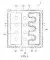
- FIG. 1 is a schematic top view of a light-emitting device 1 of a first embodiment of the invention.
- FIG. 2 is a cross-sectional view of the light-emitting device of the first embodiment, taken along the line II-II in FIG. 1 .
- the light-emitting device 1 includes a substrate 100, and a semiconductor stacked body 10 provided on the substrate 100.
- the semiconductor stacked body 10 includes an n-type semiconductor layer 11 provided on the substrate 100, a light-emitting layer 12 provided on the n-type semiconductor layer 11, and a p-type semiconductor layer 13 provided on the light-emitting layer 12.
- the substrate 100 is transmissive to the light emitted by the light-emitting layer 12.
- the semiconductor stacked body 10 can be epitaxially grown on the substrate 100.
- sapphire, spinel (MgAl 2 O 4 ), silicon carbide (SiC), silicon, ZnS, ZnO, GaAs, diamond, lithium niobate, neodymium gallate, etc. are examples of the material of the substrate 100.
- the semiconductor stacked body 10 includes, for example, a semiconductor such as In X Al Y Ga 1- X - Y N (0 ⁇ X , 0 ⁇ Y , and X + Y ⁇ 1), etc.
- the n-type semiconductor layer 11 has a light extraction surface 11a, and an n-side contact surface 11b provided on the side opposite to the light extraction surface 11a.
- the light extraction surface 11a is positioned at the interface between the n-type semiconductor layer 11 and the substrate 100.
- the light from the light extraction surface 11a passes through the substrate 100 and is extracted from mainly the side surface of the substrate 100.
- the light from the light-emitting layer 12 is extracted mainly from the side surface of the substrate 100.
- the light-emitting layer 12 and the p-type semiconductor layer 13 are not provided at the n-side contact surface 11b.
- the n-type semiconductor layer 11, the light-emitting layer 12, and the p-type semiconductor layer 13 are epitaxially grown in order on the substrate 100, and subsequently, the n-side contact surface 11b is formed by performing etching to remove a portion of the stacked portion of the p-type semiconductor layer 13 and the light-emitting layer 12.
- the portion where the p-type semiconductor layer 13 and the light-emitting layer 12 are stacked remains in a mesa-shaped configuration on the n-type semiconductor layer 11.
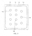
- FIG. 3 is a schematic top view of the semiconductor stacked body 10.
- FIG. 3 is a top view as viewed from the side opposite to the light extraction surface 11a shown in FIG. 2 .
- n-side contact surfaces 11b that have circular configurations are provided in the surface of the n-type semiconductor layer 11 on the side opposite to the light extraction surface 11a.
- the light-emitting layer 12 and the p-type semiconductor layer 13 are provided at a region of the surface of the n-type semiconductor layer 11 on the side opposite to the light extraction surface 11a other than the n-side contact surface 11b and an outer perimeter region 11c.
- the light-emitting layer 12 and the p-type semiconductor layer 13 are provided to surround the n-side contact surfaces 11b.
- a first p-side electrode 21 is provided on the p-type semiconductor layer 13.
- the first p-side electrode 21 contacts the upper surface of the p-type semiconductor layer 13.
- An insulating film 41 is provided on the p-type semiconductor layer 13 to cover the upper surfaces of the first p-side electrode 21 and the p-type semiconductor layer 13.
- An insulating film 42 is provided to cover the insulating film 41.
- the insulating film 42 covers the side surface of the p-type semiconductor layer 13, the side surface of the light-emitting layer 12, and the side surface of the n-type semiconductor layer 11 continuing from the side surfaces of the p-type semiconductor layer 13 and the light-emitting layer 12.
- the insulating film 42 covers the side surface of a mesa-shaped portion 15, which is the portion where the light-emitting layer 12 and the p-type semiconductor layer 13 are stacked.
- n-side electrode 22 is provided on the insulating film 42.
- the insulating film 42 has steps covering the side surfaces of the members, and the n-side electrode 22 is provided along the steps.
- the n-side electrode 22 includes an n-contact portion 22a contacting the n-side contact surface 11b, an external connection portion 22c provided on the insulating film 42 on the mesa-shaped portion 15, and an outer perimeter contact portion 22b contacting the outer perimeter region 11c of the n-type semiconductor layer 11.
- the n-contact portion 22a, the external connection portion 22c, and the outer perimeter contact portion 22b are connected as one body.
- n-side post electrode 32 is provided on the external connection portion 22c.
- the n-side post electrode 32 is electrically connected to the n-type semiconductor layer 11 via the n-side electrode 22.
- An opening is made in a portion of the insulating films 41 and 42 covering the first p-side electrode 21; and a second p-side electrode 23 is provided in the opening.
- the second p-side electrode 23 contacts the first p-side electrode 21.
- a portion of the second p-side electrode 23 is provided on the insulating film 42.
- a p-side post electrode 31 is provided on the second p-side electrode 23. The p-side post electrode 31 is electrically connected to the p-type semiconductor layer 13 via the second p-side electrode 23 and the first p-side electrode 21.
- FIG. 4 is a schematic enlarged cross-sectional view of the region of the light-emitting device 1 where the n-side contact surface 11b is provided.
- an insulating film 43 is provided in a region of the circular n-side contact surface 11b including the central portion.
- the n-side contact surface 11b includes the region including the central portion, and a region surrounding the periphery of the region including the central portion.
- the "region including the central portion” is a region including the center of the circle.
- the "region including the central portion” is a region including the center of the inscribed circle of the polygon.
- the "region including the central portion” is a region including the center of the circle formed by the inner or outer perimeter of the circular ring.
- FIG. 5 is a schematic plan view showing the arrangement, in a plan view, of the n-side contact surface 11b, the insulating film 43, and the n-contact portion 22a of the n-side electrode 22.
- the insulating film 42 is formed to cover the entire semiconductor stacked body 10.
- the insulating film 42 is patterned so that the insulating film 43 remains in, for example, a circular configuration at the n-side contact surface 11b. Accordingly, the insulating film 42 and the insulating film 43 are films of the same type of material.
- the film thickness of the insulating film 42 and the film thickness of the insulating film 43 are substantially the same.
- a portion 42a of the insulating film 42 remains in, for example, a circular ring configuration at the outer perimeter region of the n-side contact surface 11b.
- the n-contact portion 22a of the n-side electrode 22 is provided at the periphery of the insulating film 43 and is provided in, for example, a circular ring configuration surrounding the circular insulating film 43.
- the trapezoid includes an upper base 43a, and a lower base 43b that is longer than the upper base 43a.
- the lower base 43b is positioned at the interface with the n-side contact surface 11b.
- the first p-side electrode 21 it is favorable for the first p-side electrode 21 to include, for example, Ag, Al, Ni, Ti, or Pt, or an alloy including these metals as major components.
- the first p-side electrode 21 may be a single layer or a stack of these metal materials.
- the n-side electrode 22 and the second p-side electrode 23 are obtained by patterning a film of the same metal material. It is favorable for the n-side electrode 22 and the second p-side electrode 23 to include, for example, Ag, Al, Ni, Rh, Au, Cu, Ti, Pt, Pd, Mo, Cr, or W, or an alloy including these metals as major components.
- the n-side electrode 22 and the second p-side electrode 23 may be single layers or stacks of these metal materials.
- the n-side electrode 22 and the second p-side electrode 23 each include, for example, an Al film, a Ti film, a Pt film, and a Au film formed in order from the foundation interface side.
- the n-side post electrode 32 and the p-side post electrode 31 prefferably include, for example, a metal such as Cu, Au, Ni, etc.
- the n-side post electrode 32 and the p-side post electrode 31 can be formed by electroplating.
- the insulating film 41 is, for example, a silicon nitride film.
- the insulating film 41 prevents, for example, the migration of Ag included in the first p-side electrode 21.
- the insulating film 42 and the insulating film 43 are, for example, silicon oxide films.
- the n-side post electrode 32 and the p-side post electrode 31 are bonded via a conductive material such as, for example, solder, etc., to pads formed on a wiring substrate where the light-emitting device 1 is mounted.
- a conductive material such as, for example, solder, etc.
- the substrate 100 and the light extraction surface 11a of the n-type semiconductor layer 11 face upward from the wiring substrate in a state in which the n-side post electrode 32 and the p-side post electrode 31 face the wiring substrate.
- the substrate 100 may not be provided.
- the light that is emitted from the light-emitting layer 12 is extracted to the outside via the light extraction surface 11a.
- the greater part of the region on the side opposite to the light extraction surface 11a is covered with the metal films of the p-side electrodes 21 and 23 and the n-side electrode 22 (including, for example, Ag and Al which have good light reflectivity). Therefore, the light that is not oriented directly toward the light extraction surface 11a from the light-emitting layer 12 and the light that is reflected at the interface between the n-type semiconductor layer 11 and the substrate 100 can be oriented toward the light extraction surface 11a by being reflected by the metal films.
- the n-side electrode 22 is not provided; and the insulating film 43 is provided. Therefore, at the region including the central portion of the n-side contact surface 11b, the light absorption by the metal included in the n-side electrode 22 can be reduced; and the total internal reflection component at the interface between the insulating film 43 and the n-type semiconductor layer 11 can be increased. This increases the reflectance at the n-side contact surface 11b of the light propagating through the n-type semiconductor layer 11 toward the n-side contact surface 11b and increases the light extraction efficiency from the light extraction surface 11a side.
- FIG. 6 is a graph of a simulation of the relationship between a forward voltage Vf at 1000 mA and the surface area of the n-contact portion 22a of the n-side electrode 22 contacting the n-side contact surface 11b.
- ⁇ 1 illustrates the change of Vf with respect to the decrease of the surface area of the n-contact portion 22a accompanying a decrease of the diameter ⁇ 1 of the n-side contact surface 11b shown in FIG. 5 .
- ⁇ 2 illustrates the change of Vf with respect to the decrease of the surface area of the n-contact portion 22a accompanying an increase of the diameter ⁇ 2 of the insulating film 43 shown in FIG. 5 .
- the portion 42a of the insulating film 42 shown in FIG. 4 is not provided at the outer perimeter region of the n-side contact surface 11b. Accordingly, the surface area of the n-contact portion 22a is the surface area of the insulating film 43 subtracted from the surface area of the n-side contact surface 11b.
- FIG. 7 is a graph of a simulation of the relationship between the diameter ⁇ 2 of the insulating film 43 and the forward voltage Vf at 1000 mA.
- FIG. 7 illustrates the average value of the forward voltage Vf.
- FIG. 8 is a graph of a simulation of the relationship between the diameter ⁇ 2 of the insulating film 43 and a light intensity Po at 1000 mA.
- FIG. 8 illustrates the average value of the light intensity Po.
- the diameter ⁇ 1 of the n-side contact surface 11b is fixed at 21 ⁇ m.
- the portion 42a of the insulating film 42 shown in FIG. 4 is not provided at the outer perimeter region of the n-side contact surface 11b.
- the light intensity Po can be increased due to the increase of the total internal reflection region of the insulating film 43 while maintaining a forward voltage Vf equivalent to when ⁇ 2 is 0 ⁇ m (when the insulating film 43 is not provided at the n-side contact surface 11b).
- the light extraction efficiency can be increased while suppressing the increase of the forward voltage Vf.
- the configurations of the n-side contact surface 11b and the insulating film 43 are not limited to circular configurations, and may be polygonal configurations.
- the configuration of the n-contact portion 22a provided at the periphery of the insulating film 43 can be a circular ring without corners.
- the current density distribution can be easily made uniform using the n-contact portion 22a having such a configuration.
- the cross-sectional configuration of the insulating film 43 is a trapezoid as shown in FIG. 4 , a large interface region between the lower surface (the lower base of the trapezoid) 43b of the insulating film 43 and the n-type semiconductor layer 11 can be ensured. Thereby, the coverage of the n-side electrode 22 for the insulating film 43 can be better than that in the case in which the cross-sectional configuration of the insulating film 43 is, for example, a rectangle.
- FIG. 9 is a schematic plan view showing another arrangement pattern of the components shown in FIG. 5 .
- the n-contact portion 22a is not limited to being continuous along the direction surrounding the periphery of the insulating film 43, and may have a broken line configuration.
- the insulating film 43 that remains in an island configuration at the central portion of the n-side contact surface 11b can be connected to the portion 42a of the insulating film 42 which is provided in a wide region to cover the mesa-shaped portion 15, and peeling of the insulating film 43 can be suppressed.
- FIG. 10 is a schematic top view of the semiconductor stacked body 10 of the light-emitting device of a second embodiment of the invention.
- FIG. 11 is a schematic enlarged cross-sectional view of the region of the second light-emitting device where the n-side contact surface 11b is provided.
- the n-side contact surface 11b is formed in a circular ring configuration.
- a part of the semiconductor stacked body 10 is provided on a region surrounded by the n-side contact surface 11b.
- the part of the semiconductor stacked body 10 is a mesa-shaped portion 15 where the light-emitting layer 12 and the p-type semiconductor layer 13 are stacked.
- the mesa-shaped portion 15 protrudes from the n-side contact surface 11b.
- the insulating film 43 covers a top surface and a side surface of the mesa-shaped portion 15.
- the insulating film 43 is provided directly on the side surface of the mesa-shaped portion 15.
- the insulating film 41 and the first p-side electrode 21 are provided between the insulating film 43 and the top surface of the mesa-shaped portion 15.
- the insulating film 43 may be provided directly on the top surface of the mesa-shaped portion 15 without the insulating film 41 and the first p-side electrode 21 between the insulating film 43 and the top surface of the mesa-shaped portion 15.
- the n-side electrode 22 is provided on the insulating film 43.
- the n-contact portion 22a of the n-side electrode 22 contacts the circular ring shaped n-side contact surface 11b surrounding the mesa-shaped portion 15. Or, as shown in FIG. 12 , the n-side electrode 22 may not be provided on the insulating film 43 surrounded by the n-side contact surface 11b.
- the three-dimensional insulating film 43 covering the top surface and the side surface of the mesa-shaped portion 15 increases an area of the insulating film 43 in a region including the central portion of the n-side contact surface 11b compared to the planar insulating film 43 shown in FIG. 4 . This increases a total reflection light by the insulating film 43 of the emitted light of the light-emitting layer 12 in a region including the central portion of the n-side contact surface 11b.
- a reflecting film 24 may be provided between the insulating film 43 and the mesa-shaped portion 15. It is favorable for the reflecting film 24 to include, for example, Ag, Al, or an alloy including these metals as major components.
- the insulating film 43 covers the reflecting film 24. The insulating film 43 prevents the migration of the metal when the reflecting film 24 includes the metal such as Ag or Al.
- a part 11d of the n-type semiconductor layer 11 may be provided on a region surrounded by the n-side contact surface 11b.
- the part 11d of the n-type semiconductor layer 11 does not include the light-emitting layer 12 and the p-type semiconductor layer 13.
- the part 11d of the n-type semiconductor layer 11 protrudes from the n-side contact surface 11b.
- the insulating film 43 is provided directly on a top surface and a side surface of the part 11d of the n-type semiconductor layer 11.
- the step between the n-side contact surface 11b and the top surface of the part 11d of the n-type semiconductor layer 11 can be smaller than the step between the n-side contact surface 11b and the top surface of the above mesa-shaped portion 15.
- the insulating film 43 can be easily formed with superior coverage compare to the large step.
- the reflecting film 24 shown in FIG. 13 may be provided between the top and side surfaces of the part 11d of the n-type semiconductor layer 11 and the insulating film 43.
Landscapes
- Led Devices (AREA)
Applications Claiming Priority (2)
| Application Number | Priority Date | Filing Date | Title |
|---|---|---|---|
| JP2018085386 | 2018-04-26 | ||
| JP2019062394A JP7054430B2 (ja) | 2018-04-26 | 2019-03-28 | 発光素子 |
Publications (1)
| Publication Number | Publication Date |
|---|---|
| EP3561884A1 true EP3561884A1 (de) | 2019-10-30 |
Family
ID=66248610
Family Applications (1)
| Application Number | Title | Priority Date | Filing Date |
|---|---|---|---|
| EP19170592.0A Pending EP3561884A1 (de) | 2018-04-26 | 2019-04-23 | Lichtemittierende vorrichtung |
Country Status (3)
| Country | Link |
|---|---|
| US (1) | US11043614B2 (de) |
| EP (1) | EP3561884A1 (de) |
| CN (1) | CN110416381B (de) |
Citations (4)
| Publication number | Priority date | Publication date | Assignee | Title |
|---|---|---|---|---|
| US20150263236A1 (en) * | 2014-03-11 | 2015-09-17 | Kabushiki Kaisha Toshiba | Semiconductor light emitting element |
| US20160315225A1 (en) * | 2015-04-27 | 2016-10-27 | Nichia Corporation | Light emitting device |
| US20170141260A1 (en) * | 2015-11-13 | 2017-05-18 | Epistar Corporation | Light-emitting device |
| US9887334B1 (en) * | 2016-08-03 | 2018-02-06 | Samsung Electronics Co., Ltd. | Semiconductor light emitting device |
Family Cites Families (16)
| Publication number | Priority date | Publication date | Assignee | Title |
|---|---|---|---|---|
| TWI404227B (zh) * | 2005-12-20 | 2013-08-01 | Semiconductor Energy Lab | 半導體裝置及其製造方法、以及顯示裝置和電子設備 |
| CN102779918B (zh) | 2007-02-01 | 2015-09-02 | 日亚化学工业株式会社 | 半导体发光元件 |
| JP5130730B2 (ja) | 2007-02-01 | 2013-01-30 | 日亜化学工業株式会社 | 半導体発光素子 |
| JP4882792B2 (ja) * | 2007-02-25 | 2012-02-22 | 日亜化学工業株式会社 | 半導体発光素子 |
| JP2009164423A (ja) * | 2008-01-08 | 2009-07-23 | Nichia Corp | 発光素子 |
| JP5217787B2 (ja) * | 2008-08-27 | 2013-06-19 | 日亜化学工業株式会社 | 半導体発光素子 |
| JP5333382B2 (ja) * | 2010-08-27 | 2013-11-06 | 豊田合成株式会社 | 発光素子 |
| JP5849388B2 (ja) | 2010-11-04 | 2016-01-27 | サンケン電気株式会社 | 半導体発光装置 |
| KR101179606B1 (ko) | 2011-03-03 | 2012-09-05 | 주식회사 세미콘라이트 | 반도체 발광소자 |
| JP2013048200A (ja) * | 2011-07-26 | 2013-03-07 | Mitsubishi Chemicals Corp | GaN系LED素子 |
| KR101493321B1 (ko) * | 2012-11-23 | 2015-02-13 | 일진엘이디(주) | 전류 분산 효과가 우수한 발광소자 및 그 제조 방법 |
| JP6485019B2 (ja) * | 2013-12-19 | 2019-03-20 | 日亜化学工業株式会社 | 半導体発光素子 |
| JP6160726B2 (ja) | 2015-04-27 | 2017-07-12 | 日亜化学工業株式会社 | 発光装置 |
| DE102015107577A1 (de) * | 2015-05-13 | 2016-11-17 | Osram Opto Semiconductors Gmbh | Optoelektronischer Halbleiterchip |
| JP6260640B2 (ja) * | 2015-05-22 | 2018-01-17 | 日亜化学工業株式会社 | 発光素子 |
| KR102443694B1 (ko) | 2016-03-11 | 2022-09-15 | 삼성전자주식회사 | 전류 확산 특성 및 광 추출 효율을 향상시킬 수 있는 발광 소자 |
-
2019
- 2019-04-23 EP EP19170592.0A patent/EP3561884A1/de active Pending
- 2019-04-23 CN CN201910327489.6A patent/CN110416381B/zh active Active
- 2019-04-25 US US16/395,135 patent/US11043614B2/en active Active
Patent Citations (4)
| Publication number | Priority date | Publication date | Assignee | Title |
|---|---|---|---|---|
| US20150263236A1 (en) * | 2014-03-11 | 2015-09-17 | Kabushiki Kaisha Toshiba | Semiconductor light emitting element |
| US20160315225A1 (en) * | 2015-04-27 | 2016-10-27 | Nichia Corporation | Light emitting device |
| US20170141260A1 (en) * | 2015-11-13 | 2017-05-18 | Epistar Corporation | Light-emitting device |
| US9887334B1 (en) * | 2016-08-03 | 2018-02-06 | Samsung Electronics Co., Ltd. | Semiconductor light emitting device |
Also Published As
| Publication number | Publication date |
|---|---|
| US20190334062A1 (en) | 2019-10-31 |
| CN110416381B (zh) | 2025-04-25 |
| CN110416381A (zh) | 2019-11-05 |
| US11043614B2 (en) | 2021-06-22 |
Similar Documents
| Publication | Publication Date | Title |
|---|---|---|
| JP7853658B2 (ja) | 発光素子 | |
| CN108063173B (zh) | 发光元件及其制造方法 | |
| US11271146B2 (en) | Semiconductor light emitting element | |
| JP2016208012A (ja) | 発光装置 | |
| JP2003017757A (ja) | フリップチップ形半導体発光素子 | |
| US9553238B2 (en) | Method of manufacturing light emitting element | |
| CN210516746U (zh) | 发光元件 | |
| JP7054430B2 (ja) | 発光素子 | |
| US11043614B2 (en) | Light-emitting device | |
| JP7506327B2 (ja) | 発光素子、発光素子の製造方法、及び発光装置 | |
| EP2228837B1 (de) | Lichtemittierendes Bauelement, Herstellungsverfahren dafür und lichtemittierende Vorrichtung | |
| TWI764528B (zh) | 發光元件及其製造方法 | |
| JP7525787B2 (ja) | 発光装置 | |
| US12408493B2 (en) | Light-emitting element including first semiconductor layer having exposed portion with first region and second regions | |
| WO2025243570A1 (ja) | 発光素子の製造方法及び発光素子 | |
| CN113555482A (zh) | 发光元件及其制造方法 | |
| TW202230832A (zh) | 發光元件及其製造方法 |
Legal Events
| Date | Code | Title | Description |
|---|---|---|---|
| PUAI | Public reference made under article 153(3) epc to a published international application that has entered the european phase |
Free format text: ORIGINAL CODE: 0009012 |
|
| STAA | Information on the status of an ep patent application or granted ep patent |
Free format text: STATUS: THE APPLICATION HAS BEEN PUBLISHED |
|
| AK | Designated contracting states |
Kind code of ref document: A1 Designated state(s): AL AT BE BG CH CY CZ DE DK EE ES FI FR GB GR HR HU IE IS IT LI LT LU LV MC MK MT NL NO PL PT RO RS SE SI SK SM TR |
|
| AX | Request for extension of the european patent |
Extension state: BA ME |
|
| STAA | Information on the status of an ep patent application or granted ep patent |
Free format text: STATUS: REQUEST FOR EXAMINATION WAS MADE |
|
| 17P | Request for examination filed |
Effective date: 20200327 |
|
| RBV | Designated contracting states (corrected) |
Designated state(s): AL AT BE BG CH CY CZ DE DK EE ES FI FR GB GR HR HU IE IS IT LI LT LU LV MC MK MT NL NO PL PT RO RS SE SI SK SM TR |
|
| STAA | Information on the status of an ep patent application or granted ep patent |
Free format text: STATUS: EXAMINATION IS IN PROGRESS |
|
| 17Q | First examination report despatched |
Effective date: 20211223 |
|
| P01 | Opt-out of the competence of the unified patent court (upc) registered |
Effective date: 20230522 |