EP3554845B1 - Anordnung zur binären farbentwicklung (bid) für liquid-electrophotography (lep)-druckvorrichtung - Google Patents
Anordnung zur binären farbentwicklung (bid) für liquid-electrophotography (lep)-druckvorrichtung Download PDFInfo
- Publication number
- EP3554845B1 EP3554845B1 EP17894841.0A EP17894841A EP3554845B1 EP 3554845 B1 EP3554845 B1 EP 3554845B1 EP 17894841 A EP17894841 A EP 17894841A EP 3554845 B1 EP3554845 B1 EP 3554845B1
- Authority
- EP
- European Patent Office
- Prior art keywords
- ink
- exterior coating
- pip
- roller
- bid
- Prior art date
- Legal status (The legal status is an assumption and is not a legal conclusion. Google has not performed a legal analysis and makes no representation as to the accuracy of the status listed.)
- Active
Links
Images


Classifications
-
- G—PHYSICS
- G03—PHOTOGRAPHY; CINEMATOGRAPHY; ANALOGOUS TECHNIQUES USING WAVES OTHER THAN OPTICAL WAVES; ELECTROGRAPHY; HOLOGRAPHY
- G03G—ELECTROGRAPHY; ELECTROPHOTOGRAPHY; MAGNETOGRAPHY
- G03G15/00—Apparatus for electrographic processes using a charge pattern
- G03G15/06—Apparatus for electrographic processes using a charge pattern for developing
- G03G15/10—Apparatus for electrographic processes using a charge pattern for developing using a liquid developer
- G03G15/104—Preparing, mixing, transporting or dispensing developer
-
- C—CHEMISTRY; METALLURGY
- C09—DYES; PAINTS; POLISHES; NATURAL RESINS; ADHESIVES; COMPOSITIONS NOT OTHERWISE PROVIDED FOR; APPLICATIONS OF MATERIALS NOT OTHERWISE PROVIDED FOR
- C09D—COATING COMPOSITIONS, e.g. PAINTS, VARNISHES OR LACQUERS; FILLING PASTES; CHEMICAL PAINT OR INK REMOVERS; INKS; CORRECTING FLUIDS; WOODSTAINS; PASTES OR SOLIDS FOR COLOURING OR PRINTING; USE OF MATERIALS THEREFOR
- C09D11/00—Inks
- C09D11/02—Printing inks
-
- G—PHYSICS
- G03—PHOTOGRAPHY; CINEMATOGRAPHY; ANALOGOUS TECHNIQUES USING WAVES OTHER THAN OPTICAL WAVES; ELECTROGRAPHY; HOLOGRAPHY
- G03G—ELECTROGRAPHY; ELECTROPHOTOGRAPHY; MAGNETOGRAPHY
- G03G15/00—Apparatus for electrographic processes using a charge pattern
- G03G15/06—Apparatus for electrographic processes using a charge pattern for developing
- G03G15/10—Apparatus for electrographic processes using a charge pattern for developing using a liquid developer
- G03G15/11—Removing excess liquid developer, e.g. by heat
-
- G—PHYSICS
- G03—PHOTOGRAPHY; CINEMATOGRAPHY; ANALOGOUS TECHNIQUES USING WAVES OTHER THAN OPTICAL WAVES; ELECTROGRAPHY; HOLOGRAPHY
- G03G—ELECTROGRAPHY; ELECTROPHOTOGRAPHY; MAGNETOGRAPHY
- G03G9/00—Developers
-
- G—PHYSICS
- G03—PHOTOGRAPHY; CINEMATOGRAPHY; ANALOGOUS TECHNIQUES USING WAVES OTHER THAN OPTICAL WAVES; ELECTROGRAPHY; HOLOGRAPHY
- G03G—ELECTROGRAPHY; ELECTROPHOTOGRAPHY; MAGNETOGRAPHY
- G03G15/00—Apparatus for electrographic processes using a charge pattern
- G03G15/06—Apparatus for electrographic processes using a charge pattern for developing
- G03G15/08—Apparatus for electrographic processes using a charge pattern for developing using a solid developer, e.g. powder developer
- G03G15/0806—Apparatus for electrographic processes using a charge pattern for developing using a solid developer, e.g. powder developer on a donor element, e.g. belt, roller
- G03G15/0818—Apparatus for electrographic processes using a charge pattern for developing using a solid developer, e.g. powder developer on a donor element, e.g. belt, roller characterised by the structure of the donor member, e.g. surface properties
-
- G—PHYSICS
- G03—PHOTOGRAPHY; CINEMATOGRAPHY; ANALOGOUS TECHNIQUES USING WAVES OTHER THAN OPTICAL WAVES; ELECTROGRAPHY; HOLOGRAPHY
- G03G—ELECTROGRAPHY; ELECTROPHOTOGRAPHY; MAGNETOGRAPHY
- G03G2215/00—Apparatus for electrophotographic processes
- G03G2215/06—Developing structures, details
- G03G2215/0634—Developing device
Definitions
- Electrophotography is a printing technique first employed by laser printers, in which toner is applied to a drum in accordance with an electrostatic image that has been formed on the drum, and then subsequently transferred to a medium. More recently, electrophotography has been leveraged for use with liquid ink, in a process referred to as liquid electrophotography (LEP). LEP technology can equal or exceed the print quality of conventional offset lithographic and flexographic printing processes.
- liquid electrophotography is a printing technology that employs liquid ink instead of (typically dry) toner as in laser printing and other conventional electrophotography technologies.
- electrically charged liquid ink is transferred to a roller assembly referred to as a binary ink developer (BID) assembly, which includes a developer roller and which increases the concentration of solids such as resin and pigments within the liquid ink.
- BID binary ink developer
- the ink is transferred to a photoconductive imaging cylinder, referred to as a print-imaging plate (PIP), in accordance with an electrostatic latent image on the cylinder.
- PIP print-imaging plate
- the ink is then transferred from the PIP to a heated blanket cylinder, or warming blanket, which evaporates carrier liquids and transforms the liquid ink into a hot melt, which is almost 100% solid, before the ink is finally transferred to media being advanced via an impression drum.
- the liquid ink is negatively charged prior to the BID assembly and BID assembly increases the solid concentration of the ink.
- the PIP is also negatively charged, but more so than the ink, and is selectively discharged in accordance with the image to be formed on a medium.
- the liquid ink is thus attracted to areas of the PIP that have been selectively discharged, while being repelled from those areas that have not. In this way, the liquid ink is transferred to the PIP in accordance with the image to be formed on a medium.
- the pigments in the ink that ultimately are transferred to a medium may be those that correspond to color components that permit a full color image to be created on the medium.
- the different colors may be cyan, magenta, yellow, and black, or cyan, light cyan, magenta, light magenta, yellow, and black to provide more accurate color rendition.
- the developer roller is biased with a specific voltage, such as -450 volts, and has compacted negatively charged ink on its exterior surface.
- a specific voltage such as -450 volts
- the developer roller meets the PIP, which is itself biased at a lower voltage, such as -1,000 volts at background portions of the image
- a positive charge is induced at the exterior surface of the developer roller to satisfy an electrostatic voltage boundary condition of the developer roller.
- conductive inks are just that - electrically conductive - this positive charge can bleed into the ink, resulting in changes in ink polarity from negative to positive.
- a developer roller includes an electrically insulating exterior coating surrounding an electrically conductive rubber roller, which itself can include a conductive metal core.
- the techniques described herein place negative charges on the exterior surface of the assembly to negatively charge the ink. No positive charge can bleed into the ink, because there is no positive charge on the developer roller. No ink polarity changes occur that can cause transfer of conductive ink onto the PIP at background portions of the image, mitigating if not eliminating print artifacts that result from such an electric field.
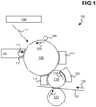
- FIG. 1 shows an example LEP printing device 100.
- the printing device 100 includes a PIP 102, which is more generally a photoconductive imaging cylinder.
- the PIP 102 rotates counterclockwise as indicated by arrow 104.
- the PIP 102 rotates past a charge roller 106 of the printing device 100, which negatively charges the PIP 102.
- a laser 108 or other discharge mechanism of the printing device 100 selectively discharges the PIP 102 via a laser beam 110 or other optical beam, in accordance with an image to be formed on a print medium like paper, as the PIP 102 rotates past the laser beam 110 and the laser 110 beam is normal to the PIP 102. Therefore, an electrostatic latent image is formed on the PIP 102.
- the LEP printing device 100 includes a BID assembly 112. There can be more than one BID assembly 112, rotationally arranged the PIP 102 counterclockwise from the depicted BID assembly 112 in FIG. 1 . Each BID assembly 112 corresponds to a different color or type of ink.
- the BID assembly 112 includes a developer roller 113 rotating clockwise as indicated by arrow 115 to transfer electrically charged liquid ink onto the PIP 102 in accordance with the electrostatic image on the PIP 102 by the laser beam 110 of the laser 108.
- the ink is electrically attracted to the PIP 102, and is not electrically attracted to the PIP 102 where the image is not to be formed on the medium, which is a background portion of the image.
- the PIP 102 rotates past a pre-transfer discharge unit 114 of the LEP printing device 100, which electrically discharges remaining charge corresponding to the background portion of the prior electrostatic image on the PIP 102.
- the printing device 100 includes a blanket 116, which is also referred to as a blanket cylinder, which rotates counterclockwise as indicated by the arrow 118.
- the blanket 116 rotates past a heating mechanism 120 that heats the blanket 116.
- the heated blanket 116 and the PIP 102 contact one another as they rotate, which transfers the ink from the PIP 102 to the heated blanket 116.
- the heated blanket 116 reduces the liquid content of the ink, rendering the ink as a sticky film on the blanket 116.
- the PIP 102 continues to rotate past a cleaning station 128, which removes any ink residue from the PIP 102 and prepares it for another rotation past the charge roller 106.
- the cleaning station 128 may include a wetting roller to wet the PIP 102, and a sponge and a wiper to then remove the wetted ink residue from the PIP 102, for instance.
- the LEP printing device 100 includes an impression cylinder 121, or impression drum, which rotates clockwise as indicated by arrow 122. Rotation of the impression cylinder 121, together with rotation of the blanket 116, advances a print medium 124, like paper, in the direction indicated by arrow 126. The film of ink is transferred from the blanket 116 onto the medium 124 against the impression cylinder 121, as the medium 124 advances between the impression cylinder 121 and the blanket 116.
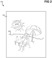
- FIG. 2 shows an example image 200 that can be formed on the print medium 124 by the LEP printing device 100.
- the image 200 includes an image portion 202 and a background portion 204.
- the image portion 202 includes those parts of the image 200 corresponding to ink - that is, where the image 200 is actively printed on the print medium 124 by the printing device 100.
- the background portion 204 includes those parts of the image 200 that do not correspond to ink - that is, where the image 200 is not actively printed by the device 100.
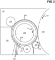
- FIG. 3 shows the example BID assembly 112 of the LEP printing device 100.
- the developer roller 113 of the BID assembly 112 includes a conductive rubber roller 308 having a conductive core roller 302, and an electrical insulating exterior coating 306 around the roller 308.
- the developer roller 113 rotates clockwise as indicated by arrow 115.
- the exterior coating 306 can have a thickness between two or three micrometres and tens of micrometres, such as between ten and eighteen micrometres. More generally, the exterior coating 306 has a thickness in micrometres having an order of magnitude between zero and one.
- the exterior coating 306 may be fabricated from a poly (p-xylylene) polymer, or another material.
- the BID assembly 112 includes a charger roller 310, which is not to be confused with the separate charge roller 106 for the PIP 102 in FIG. 1 .
- the charge roller 310 is in contact with the electrically insulating exterior coating 306 and places a negative charge on the exterior coating 306 as the developer roller 113 rotates past the charge roller 310.
- Liquid ink 320 initially has a low percentage of solids, such as resins and pigments.
- the liquid ink 320 can include negatively charged ink particles and counter charges in the form of positive micelles.
- the liquid ink 320 which thus has a zero total charge, is pumped within a channel 304 of the BID assembly 112, resulting in the negatively charged ink particles and positively charged micelles to separate due to an electric field between an electrode 301 and the developer roller 113.
- the exterior coating 306 thus receives negatively charged ink 320. That is, the electrode 301 is said to plate the negatively charged ink 320 onto the exterior coating 306.
- the developer roller 113 continues to rotate towards a squeeze roller 312 of the BID assembly 112, which is in near contact with the exterior coating 306.
- the developer roller 113 rotates past the squeeze roller 312.
- the squeeze roller 312 reduces a thickness of the liquid ink 320 on the exterior coating 306, which reduces the liquid content of the ink.
- the squeeze roller 312 compacts the ink 320 both mechanically and electrostatically.
- the liquid content of the ink 320 may be reduced from about 80% as initially plated onto the exterior coating 306 to about 75% after passing against the squeeze roller 312.
- the developer roller 113, with the reduced-thickness liquid ink 320 on its exterior coating 306, continues to rotate past the PIP 102 of the LEP printing device 100, which is rotating counterclockwise per the arrow 104.
- the ink 320 is thus transferred to image portions 202 of the electrostatic image 200 formed on the PIP 102, as described above in relation to FIG. 1 .
- the ink 320 is not transferred to the PIP 102 at background portions 204 of the image 200 because there is more negative charge on the PIP 102 than on the developer roller 113 and because the resulting electric field is directed towards the PIP 102.
- the developer roller 113 rotates past a cleaning roller 316, which rotates counterclockwise per arrow 318.
- the cleaning roller 316 removes (any) remaining ink 320 from the exterior coating 306, preparing the developer roller 113 for another rotation past the charge roller 310.
- a charge roller 310 instead places negative charges on the electrically non-conductive surface of the exterior coating 306.
- the rubber roller 308 of the developer roller 113 can be electrically conductive since it is not in direct contact with the ink 320 due to the presence of the exterior coating 306. That the roller 308 is rubber can provide a degree of flexibility or softness to the developer roller 113 of the BID assembly 112. Such flexibility or softness can lessen the potential for mechanical problems resulting when the exterior coating 306 makes contact with the PIP 102, particularly if the exterior coating 306 is itself a hard coating.
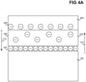
- FIG. 4A shows an example of the electrostatic charge at a background portion 204 of an electrostatic image 200 formed on the PIP 102 in relation to the electrically insulating exterior coating 306 having a layer of electrically conductive ink 320, at the location in FIG. 3 at which the developer roller 113 is in contact with the PIP 102.
- FIG. 4A thus shows a charge-specified boundary condition at the boundary between the exterior coating 306 of the developer roller 113 of the BID assembly 112 and the ink 320.
- FIG. 4A shows the PIP 102 as to a background portion 204 of an electrostatic image 200 formed on the PIP 102 because the PIP 102 still has negative charge 404 placed by the charge roller 106 of FIG. 1 .
- an image portion 202 of the image 200 formed on the PIP 102 would not have any negative charge, because the PIP 102 is optically discharged at the image portion 202 of the image 200, which is subsequently in relation to FIG. 4B below.
- the electrically insulating exterior coating 306 of the developer roller 113 has negative charge 408, placed by the charge roller 310 of FIG. 3 .
- the developer roller 113 is not, in other words, biased with a negative voltage (and its exterior coating 306 is not electrically conductive).
- the boundary condition between the ink 320 and the exterior coating 306 is a charged-specified electrostatic boundary condition, because the charge placed on the exterior coating 306 is specified (and maintained).
- the boundary condition is not a voltage-specified electrostatic boundary condition as would be the case if there were no exterior insulating coating 306 and biased with a specified negative voltage that is maintained.
- the electrically conductive ink 320 has the negative charge 406 throughout its volume. Within FIG. 4A , there is no positive charge therefore; no positive charge can thus be transferred to the ink 320 within the BID assembly 112 that includes the exterior coating 306.
- the exterior insulating coating 306 were absent and the developer roller 113 instead biased with a negative voltage, the maintenance of a voltage-specified electrostatic boundary condition between the ink 320 and the developer roller 113 would result in a positive charge being induced at the exterior coating 306.
- Such positive charge could leak into the ink 320, because the ink 320 is conductive, resulting in the ink 320 transferring to the PIP 102 even at a background portion 204 of the electrostatic image 200, since the ink 320 would become positive and thus not repelled from the negative charge 406 on the PIP 102.
- a resulting electric field 410 is directed downwards, from the exterior coating 306 of the BID assembly 112 through the electrically conductive ink 320 and towards the PIP 102. This is because the charge on the exterior coating 306 is less dense than the charge on the PIP 102 at the background portion 202 of the image 200. A resulting electrostatic force 412 is thus directed upwards, from the PIP 102 towards the exterior coating 306. Therefore, the ink 320 remains on the exterior coating 306 and is not transferred to the PIP 102, since the electrostatic force 412 is directed upwards towards the exterior coating 306 and not downwards towards the PIP 102.
- FIG. 4B shows an example of the electrostatic charge at an image portion 202 of an electrostatic image 200 formed on the PIP 102 in relation to the electrically insulating exterior coating 306 having a layer of electrically conductive ink 320, at the location in FIG. 3 at which the developer roller 113 is in contact with the PIP 102.
- FIG. 4B thus shows a charge-specified boundary condition at the boundary between the exterior coating 306 of the developer roller 113 of the BID assembly 112 and the ink 320.
- FIG. 4B shows the PIP 102 as to an image portion 202 of an electrostatic image 200 formed on the PIP 102 because the PIP 102 no longer has negative charge placed by the charge roller 106 of FIG. 1 .
- a background portion 204 of the image 200 formed on the PIP 102 would have negative charge, because the PIP 102 is not optically discharged at the background portion 204 of the image 200, as previously described in relation to FIG. 4A .
- the electrically insulating exterior coating 306 of the developer roller 113 again has negative charge 408, placed by the charge roller 310 of FIG. 3 .
- the developer roller 113 is not, in other words, biased with a negative voltage (and its exterior coating 306 is not electrically conductive) in FIG. 4B . Therefore, electrostatically, the boundary condition between the ink 320 and the exterior coating 306 is in FIG. 4B a charged-specified electrostatic boundary condition, because the charge placed on the exterior coating 306 is specified (and maintained).
- the boundary condition is not a voltage-specified electrostatic boundary condition as would be the case if the exterior coating 306 were electrically conductive and biased with a specified negative voltage that is maintained.
- the electrically conductive ink 320 also has negative charge 406 in FIG. 4B throughout its volume. As in FIG. 4A , within FIG. 4B there is no positive charge therefore; no positive charge can thus be transferred to the ink 320 within the BID assembly 112 that includes the exterior coating 306. In FIG. 4B , however, a resulting electric field 450 is directed upwards, from the exterior coating 306 of the developer roller 113 through the electrically conductive ink 320 and towards the PIP 102. This is because there is no charge on the PIP 102 at the image portion 202 of the image 200, while there is negative charge 408 on the exterior coating 306. A resulting electrostatic force 452 is thus directed downwards in FIG. 4A , from the exterior coating 306 towards the PIP 102. Therefore, the ink 320 is transferred from the exterior coating 306 to the PIP 102, since the electrostatic force 102 is directed downwards towards the PIP 102.
- FIG. 5 shows an example graph 500 of the electric field in the scenario of FIG. 4 , at a background portion 204 of an electrostatic image 200 formed on the PIP 102 in relation to the exterior coating 306 having electrically conductive ink 320, at the location in FIG. 3 at which the developer roller 113 is in contact with the PIP 102.
- the axis 502 of the graph 500 denotes distance, and is spatially divided into regions corresponding to the PIP 102, the ink 320, and the electrically insulating coating 306.
- the axis 504 of the graph 500 denotes the electric field, with a zero electric field (i.e., no electric field) specifically called out in FIG. 5 .
- a solid line 508 indicates the electric field among the PIP 102, the electrically conductive ink 320, and the electrically insulating exterior coating 306 of the BID assembly 112.
- the electric field is positive at the PIP 102, and at the boundary between the PIP 102 and the electrically conductive ink 320 decreases and becomes negative.
- This discontinuity of the electric field towards negative is a representation of negative surface charges on the PIP 102.
- Electrically conductive ink 320 can have a non-conductive portion that can have a charge, rendering charge to the ink 320 as a whole.
- the non-conductive portion can be a charged polymer that can be removed in a later part of the printing process.
- the electric field becomes zero, since this portion is electrically conductive.
- the non-conductive portion of the conductive ink 320 having charge can be distributed throughout the volume of the ink 320, such that the charge itself is distributed throughout the volume, causing the electrical field to slowly decrease (i.e., for a constant volume distribution, a linear decrease).
- the electric field exhibits another negative discontinuity that represents negative surface charge on the electrically insulating exterior coating 306 of the developer roller 113 of the BID assembly 112.
- the solid line 508 therefore depicts that there is no enhancement of the electric field within the electrically conductive ink 320.
- the electric field at the non-conductive portion of the conductive ink 320 would increase. This is because the imposed voltage-specific boundary condition specifies a higher electric field to compensate for the zero electric field within the conductive portion of the ink 320.
- This enhancement of the electric field can result in electrical breakdown of the non-conductive portion of the ink 320 as well as dielectric carrier fluids (e.g., isoparaffinic fluids) within the ink 320, and therefore, positively charge the ink 320.
- FIG. 5 demonstrates how placing charge on an electrically insulating exterior coating 306 of a developer roller 113, instead of biasing a voltage on a developer roller 113 that lacks an exterior coating 306 that is electrically insulating, can minimize, if not eliminate, electric field enhancement within electrically conductive ink 320. Minimizing or eliminating this electric field enhancement in turn reduces or eliminates transfer of the electrically conductive ink 320 to the PIP 102 at a background portion 204 of the image 200 electrostatically formed on the PIP 102.
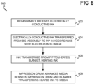
- FIG. 6 shows an example method 600 for printing an image 200 on a print medium 124 using the LEP printing device 100.
- the electrically insulating exterior coating 306 of the developer roller 113 of the BID assembly 112 receives electrically conductive ink 320 (602).
- the ink 320 is transferred from the exterior coating 306 of the developer roller 113 of the BID assembly 112 to the PIP 102 in accordance with the electrostatic image 200 (604).
- the ink 320 is transferred to the PIP 102 at image portions 202 of the image 200, and not to background portions 204 of the image 200.
- the ink 320 is then transferred from the PIP 102 to a heated blanked 116 (606).
- An impression cylinder 121 advances the media 124 between the cylinder 121 and the blanket 116, causing the heated ink 320 to be transferred from the blanket 116 to the media 124.
Landscapes
- Physics & Mathematics (AREA)
- General Physics & Mathematics (AREA)
- Chemical & Material Sciences (AREA)
- Life Sciences & Earth Sciences (AREA)
- Engineering & Computer Science (AREA)
- Materials Engineering (AREA)
- Wood Science & Technology (AREA)
- Organic Chemistry (AREA)
- Wet Developing In Electrophotography (AREA)
Claims (7)
- Anordnung eines binären Tintenentwicklers (Binary Ink Developer - BID) (112), die Folgendes umfasst:eine Entwicklerwalze (113), die drehbar ist;eine elektrisch isolierende äußeren Beschichtung (306) der Entwicklerwalze (113), um Tinte von einem Tintenvorrat zu empfangen und die empfangene Tinte gemäß einem elektrostatischen Bild auf dem Bildgebungszylinder (102) an einen fotoleitenden Bildgebungszylinder (102) zu übertragen, während sich die Entwicklerwalze (113) dreht, unddadurch gekennzeichnet, dass die BID-Anordnung (112) ferner Folgendes umfasst:eine Ladewalze (310) in Kontakt mit der elektrisch isolierenden äußeren Beschichtung (306), um eine Ladung auf der äußeren Beschichtung (306) zu platzieren, bevor die äußere Beschichtung (306) die Tinte empfängt,wobei die äußere Beschichtung (306) innerhalb der BID-Anordnung (112) nicht spannungsvorgespannt ist.
- BID-Anordnung (112) nach Anspruch 1, wobei die elektrisch isolierende äußere Beschichtung (306) eine Dicke in Mikrometer aufweist, die eine Größenordnung zwischen null und eins aufweisen.
- BID-Anordnung (112) nach Anspruch 1, die ferner Folgendes umfasst:eine Quetschwalze (312) in einem drehbaren Kontakt mit der elektrisch isolierenden äußeren Beschichtung (306), um eine Dicke der Tinte, die auf der äußeren Beschichtung (306) empfangen wird, vor einer Übertragung der empfangenen Tinte an den fotoleitenden Bildgebungszylinder (102) zu verringern; undeine Reinigungswalze (316) in drehbarem Kontakt mit der äußeren Beschichtung (306), um beliebige Resttinte von der äußeren Beschichtung (306) nach der Übertragung der empfangenen Tinte an den Bildgebungszylinder (102) zu entfernen.
- Flüssig-Elektrofotographie(Liquid Electrography - LEP)-Druckvorrichtung (100), die Folgendes umfasst:Anordnung eines binären Tintenentwicklers (BID) (112) nach einem der Ansprüche 1 bis 3; undeinen fotoleitenden Bildgebungszylinder (102), an den die BID-Anordnung (112) die Tinte gemäß einem elektrostatischen Bild auf dem Bildgebungszylinder (102) zu übertragen hat.
- LEP-Druckvorrichtung (100) nach Anspruch 4, wobei die Tinte, die durch den Tintenvorrat an die BID-Anordnung (112) bereitgestellt wird, elektrisch leitfähige Tinte ist,
wobei keine positive Ladung durch die BID-Anordnung (112) an die elektrisch leitfähige Tinte übertragen wird. - Verfahren, das Folgendes umfasst:Empfangen, durch eine Flüssig-Elektrofotografie(LEP)-Druckvorrichtung (100) nach einem beliebigen der Ansprüche 4 bis 5, elektrisch leitfähiger Tinte, während die Entwicklerwalze (113) der LEP-Druckvorrichtung (100) in drehbarem Kontakt mit einem fotoleitenden Bildgebungszylinder (102) steht; undÜbertragen der empfangenen elektrisch leitfähigen Tinte von der Entwicklerwalze (113) an den fotoleitenden Bildgebungszylinder (102) gemäß einem elektrostatischen Bild auf dem fotoleitenden Bildgebungszylinder (102).
- Verfahren nach Anspruch 6, wobei keine positive Ladung an die elektrisch leitfähige Tinte innerhalb der BID-Anordnung (112) übertragen wird.
Applications Claiming Priority (1)
| Application Number | Priority Date | Filing Date | Title |
|---|---|---|---|
| PCT/US2017/015849 WO2018143949A1 (en) | 2017-01-31 | 2017-01-31 | Binary ink developer (bid) assembly for liquid electrophotography (lep) printing device |
Publications (3)
| Publication Number | Publication Date |
|---|---|
| EP3554845A1 EP3554845A1 (de) | 2019-10-23 |
| EP3554845A4 EP3554845A4 (de) | 2020-10-21 |
| EP3554845B1 true EP3554845B1 (de) | 2023-05-24 |
Family
ID=63040975
Family Applications (1)
| Application Number | Title | Priority Date | Filing Date |
|---|---|---|---|
| EP17894841.0A Active EP3554845B1 (de) | 2017-01-31 | 2017-01-31 | Anordnung zur binären farbentwicklung (bid) für liquid-electrophotography (lep)-druckvorrichtung |
Country Status (4)
| Country | Link |
|---|---|
| US (2) | US10459372B2 (de) |
| EP (1) | EP3554845B1 (de) |
| CN (1) | CN110267820B (de) |
| WO (1) | WO2018143949A1 (de) |
Families Citing this family (4)
| Publication number | Priority date | Publication date | Assignee | Title |
|---|---|---|---|---|
| EP3837586A4 (de) * | 2018-08-13 | 2022-03-30 | Hewlett-Packard Development Company, L.P. | Lichtempfindliche bildgebungsoberflächen |
| TWI852977B (zh) | 2019-01-10 | 2024-08-21 | 美商健生生物科技公司 | 前列腺新抗原及其用途 |
| EP4175664A2 (de) | 2020-07-06 | 2023-05-10 | Janssen Biotech, Inc. | Prostata-neoantigene und ihre verwendungen |
| US12204260B2 (en) * | 2020-10-16 | 2025-01-21 | Hewlett-Packard Development Company, L.P. | Developer roller |
Family Cites Families (15)
| Publication number | Priority date | Publication date | Assignee | Title |
|---|---|---|---|---|
| IL103705A (en) * | 1991-11-15 | 1995-12-08 | Kuehnle Manfred R | Electro-thermal printing ink and method and printing device with its help |
| JP3217509B2 (ja) | 1992-12-18 | 2001-10-09 | 株式会社リコー | 現像装置 |
| KR0174689B1 (ko) * | 1996-09-11 | 1999-04-01 | 삼성전자주식회사 | 현상롤러의 고스트 방지장치 |
| KR100622402B1 (ko) * | 2003-12-29 | 2006-09-18 | 삼성전자주식회사 | 보조 대전롤러를 구비하는 화상 형성 장치 |
| JP4378303B2 (ja) | 2005-03-03 | 2009-12-02 | 株式会社リコー | 現像装置の評価方法 |
| KR100739746B1 (ko) * | 2005-10-25 | 2007-07-13 | 삼성전자주식회사 | 전자사진방식 화상형성장치 및 현상방법 |
| US7734244B2 (en) | 2007-02-23 | 2010-06-08 | Xerox Corporation | Apparatus for conditioning a substrate |
| JP2008233419A (ja) | 2007-03-19 | 2008-10-02 | Ricoh Co Ltd | 現像装置、トナー、画像形成方法、画像形成装置及びプロセスカートリッジ |
| EP2110715B1 (de) | 2008-04-15 | 2012-06-06 | Ten Cate Enbi International B.V. | Entwicklungsrolle, Entwicklungsvorrichtung mit einer solchen Entwicklungsrolle sowie Verfahren zur Bereitstellung einer solchen Entwicklungsrolle |
| EP2296900B1 (de) | 2008-05-30 | 2014-09-10 | Hewlett-Packard Development Company | Verfahren zum messen der leitfähigkeit von tinte |
| US8750763B2 (en) | 2011-12-30 | 2014-06-10 | Lexmark International, Inc. | Charge roller for an image forming apparatus using hard filler particles |
| US10261437B2 (en) * | 2012-02-07 | 2019-04-16 | Hp Indigo B.V. | Liquid electrophotograpy |
| US9248641B2 (en) * | 2012-11-23 | 2016-02-02 | Hewlett-Packard Indigo B.V. | Ink transfer element |
| JP5336680B1 (ja) * | 2013-06-11 | 2013-11-06 | 株式会社アフィット | 導電性粒子を含有する液体現像剤及びそれを用いた導電パターン形成方法及び導電パターン形成装置 |
| CN108713169B (zh) * | 2016-04-06 | 2022-01-04 | 惠普印迪戈股份公司 | 液体电子照相墨水 |
-
2017
- 2017-01-13 US US16/076,342 patent/US10459372B2/en active Active
- 2017-01-31 EP EP17894841.0A patent/EP3554845B1/de active Active
- 2017-01-31 WO PCT/US2017/015849 patent/WO2018143949A1/en not_active Ceased
- 2017-01-31 CN CN201780085269.6A patent/CN110267820B/zh active Active
-
2019
- 2019-10-10 US US16/598,120 patent/US10901344B2/en active Active
Also Published As
| Publication number | Publication date |
|---|---|
| EP3554845A1 (de) | 2019-10-23 |
| WO2018143949A1 (en) | 2018-08-09 |
| US10459372B2 (en) | 2019-10-29 |
| CN110267820A (zh) | 2019-09-20 |
| EP3554845A4 (de) | 2020-10-21 |
| US20190041771A1 (en) | 2019-02-07 |
| CN110267820B (zh) | 2020-12-22 |
| US20200041933A1 (en) | 2020-02-06 |
| US10901344B2 (en) | 2021-01-26 |
Similar Documents
| Publication | Publication Date | Title |
|---|---|---|
| US10901344B2 (en) | Binary ink developer (BID) assembly for liquid electrophotography (LEP) printing device | |
| EP0309588B1 (de) | Verfahren zum mehrfarbigen bedrucken von metallischen behältern und metallischen blättern | |
| EP2332015B1 (de) | Druckervorrichtung mit einer entwicklungswalze | |
| US8787800B2 (en) | Apparatus to receive a developer roller | |
| EP2670597B1 (de) | Drucker sowie verfahren und vorrichtung zur erzeugung eines bildes auf einem druckträger | |
| EP2467757B1 (de) | Zwischentransferelementstuch, vorrichtung und transferverfahren | |
| US10948853B2 (en) | Liquid electro-photographic printing transfer devices | |
| KR100394380B1 (ko) | 습식형 현상장치 및 그것을 이용한 화상 형성장치 | |
| US10222719B2 (en) | Electro-photographic printing | |
| KR100462616B1 (ko) | 습식 화상형성시스템 및 그를 이용한 화상형성방법 | |
| US20200241448A1 (en) | Cleaning station sponges | |
| EP1971900B1 (de) | Vorichtung und verfahren zur minimierung von restladungseffekten bei einem drucker | |
| US20200241447A1 (en) | Printing fluid developer assembly | |
| WO2019212477A1 (en) | Optical density adjustment | |
| US8355035B2 (en) | Digital gravure printing with a pixilated photoconductor | |
| EP3676668B1 (de) | Hemmung von tintenflussstreifen | |
| EP3039489B1 (de) | Elektrofotografischer flüssigdruck | |
| US8375853B2 (en) | Transfer unit in an electrophoretic printing or copying apparatus | |
| WO2016165736A1 (en) | Liquid electrophotographic printing | |
| JPH01301279A (ja) | 容器の多色印刷方法 | |
| JP2002062714A (ja) | 液体現像フルカラー電子写真装置 | |
| JP2002040752A (ja) | 液体現像フルカラー電子写真装置 | |
| JP2001324877A (ja) | 液体現像電子写真装置 | |
| JP2001125403A (ja) | 電極式中間転写ベルトを備える直列式多色複写機 | |
| JPH01301280A (ja) | 容器の多色印刷方法 |
Legal Events
| Date | Code | Title | Description |
|---|---|---|---|
| STAA | Information on the status of an ep patent application or granted ep patent |
Free format text: STATUS: THE INTERNATIONAL PUBLICATION HAS BEEN MADE |
|
| PUAI | Public reference made under article 153(3) epc to a published international application that has entered the european phase |
Free format text: ORIGINAL CODE: 0009012 |
|
| STAA | Information on the status of an ep patent application or granted ep patent |
Free format text: STATUS: REQUEST FOR EXAMINATION WAS MADE |
|
| 17P | Request for examination filed |
Effective date: 20190716 |
|
| AK | Designated contracting states |
Kind code of ref document: A1 Designated state(s): AL AT BE BG CH CY CZ DE DK EE ES FI FR GB GR HR HU IE IS IT LI LT LU LV MC MK MT NL NO PL PT RO RS SE SI SK SM TR |
|
| AX | Request for extension of the european patent |
Extension state: BA ME |
|
| DAV | Request for validation of the european patent (deleted) | ||
| DAX | Request for extension of the european patent (deleted) | ||
| REG | Reference to a national code |
Ref country code: DE Ref legal event code: R079 Free format text: PREVIOUS MAIN CLASS: B41J0002410000 Ipc: G03G0015100000 Ref country code: DE Ref legal event code: R079 Ref document number: 602017069111 Country of ref document: DE Free format text: PREVIOUS MAIN CLASS: B41J0002410000 Ipc: G03G0015100000 |
|
| A4 | Supplementary search report drawn up and despatched |
Effective date: 20200922 |
|
| RIC1 | Information provided on ipc code assigned before grant |
Ipc: G03G 15/10 20060101AFI20200916BHEP |
|
| STAA | Information on the status of an ep patent application or granted ep patent |
Free format text: STATUS: EXAMINATION IS IN PROGRESS |
|
| 17Q | First examination report despatched |
Effective date: 20210914 |
|
| GRAP | Despatch of communication of intention to grant a patent |
Free format text: ORIGINAL CODE: EPIDOSNIGR1 |
|
| STAA | Information on the status of an ep patent application or granted ep patent |
Free format text: STATUS: GRANT OF PATENT IS INTENDED |
|
| INTG | Intention to grant announced |
Effective date: 20230302 |
|
| GRAS | Grant fee paid |
Free format text: ORIGINAL CODE: EPIDOSNIGR3 |
|
| GRAA | (expected) grant |
Free format text: ORIGINAL CODE: 0009210 |
|
| STAA | Information on the status of an ep patent application or granted ep patent |
Free format text: STATUS: THE PATENT HAS BEEN GRANTED |
|
| AK | Designated contracting states |
Kind code of ref document: B1 Designated state(s): AL AT BE BG CH CY CZ DE DK EE ES FI FR GB GR HR HU IE IS IT LI LT LU LV MC MK MT NL NO PL PT RO RS SE SI SK SM TR |
|
| REG | Reference to a national code |
Ref country code: GB Ref legal event code: FG4D |
|
| REG | Reference to a national code |
Ref country code: CH Ref legal event code: EP |
|
| REG | Reference to a national code |
Ref country code: DE Ref legal event code: R096 Ref document number: 602017069111 Country of ref document: DE |
|
| REG | Reference to a national code |
Ref country code: AT Ref legal event code: REF Ref document number: 1569895 Country of ref document: AT Kind code of ref document: T Effective date: 20230615 |
|
| REG | Reference to a national code |
Ref country code: IE Ref legal event code: FG4D |
|
| REG | Reference to a national code |
Ref country code: LT Ref legal event code: MG9D |
|
| REG | Reference to a national code |
Ref country code: NL Ref legal event code: MP Effective date: 20230524 |
|
| REG | Reference to a national code |
Ref country code: AT Ref legal event code: MK05 Ref document number: 1569895 Country of ref document: AT Kind code of ref document: T Effective date: 20230524 |
|
| PG25 | Lapsed in a contracting state [announced via postgrant information from national office to epo] |
Ref country code: SE Free format text: LAPSE BECAUSE OF FAILURE TO SUBMIT A TRANSLATION OF THE DESCRIPTION OR TO PAY THE FEE WITHIN THE PRESCRIBED TIME-LIMIT Effective date: 20230524 Ref country code: PT Free format text: LAPSE BECAUSE OF FAILURE TO SUBMIT A TRANSLATION OF THE DESCRIPTION OR TO PAY THE FEE WITHIN THE PRESCRIBED TIME-LIMIT Effective date: 20230925 Ref country code: NO Free format text: LAPSE BECAUSE OF FAILURE TO SUBMIT A TRANSLATION OF THE DESCRIPTION OR TO PAY THE FEE WITHIN THE PRESCRIBED TIME-LIMIT Effective date: 20230824 Ref country code: NL Free format text: LAPSE BECAUSE OF FAILURE TO SUBMIT A TRANSLATION OF THE DESCRIPTION OR TO PAY THE FEE WITHIN THE PRESCRIBED TIME-LIMIT Effective date: 20230524 Ref country code: ES Free format text: LAPSE BECAUSE OF FAILURE TO SUBMIT A TRANSLATION OF THE DESCRIPTION OR TO PAY THE FEE WITHIN THE PRESCRIBED TIME-LIMIT Effective date: 20230524 Ref country code: AT Free format text: LAPSE BECAUSE OF FAILURE TO SUBMIT A TRANSLATION OF THE DESCRIPTION OR TO PAY THE FEE WITHIN THE PRESCRIBED TIME-LIMIT Effective date: 20230524 |
|
| PG25 | Lapsed in a contracting state [announced via postgrant information from national office to epo] |
Ref country code: RS Free format text: LAPSE BECAUSE OF FAILURE TO SUBMIT A TRANSLATION OF THE DESCRIPTION OR TO PAY THE FEE WITHIN THE PRESCRIBED TIME-LIMIT Effective date: 20230524 Ref country code: PL Free format text: LAPSE BECAUSE OF FAILURE TO SUBMIT A TRANSLATION OF THE DESCRIPTION OR TO PAY THE FEE WITHIN THE PRESCRIBED TIME-LIMIT Effective date: 20230524 Ref country code: LV Free format text: LAPSE BECAUSE OF FAILURE TO SUBMIT A TRANSLATION OF THE DESCRIPTION OR TO PAY THE FEE WITHIN THE PRESCRIBED TIME-LIMIT Effective date: 20230524 Ref country code: LT Free format text: LAPSE BECAUSE OF FAILURE TO SUBMIT A TRANSLATION OF THE DESCRIPTION OR TO PAY THE FEE WITHIN THE PRESCRIBED TIME-LIMIT Effective date: 20230524 Ref country code: IS Free format text: LAPSE BECAUSE OF FAILURE TO SUBMIT A TRANSLATION OF THE DESCRIPTION OR TO PAY THE FEE WITHIN THE PRESCRIBED TIME-LIMIT Effective date: 20230924 Ref country code: HR Free format text: LAPSE BECAUSE OF FAILURE TO SUBMIT A TRANSLATION OF THE DESCRIPTION OR TO PAY THE FEE WITHIN THE PRESCRIBED TIME-LIMIT Effective date: 20230524 Ref country code: GR Free format text: LAPSE BECAUSE OF FAILURE TO SUBMIT A TRANSLATION OF THE DESCRIPTION OR TO PAY THE FEE WITHIN THE PRESCRIBED TIME-LIMIT Effective date: 20230825 |
|
| PG25 | Lapsed in a contracting state [announced via postgrant information from national office to epo] |
Ref country code: FI Free format text: LAPSE BECAUSE OF FAILURE TO SUBMIT A TRANSLATION OF THE DESCRIPTION OR TO PAY THE FEE WITHIN THE PRESCRIBED TIME-LIMIT Effective date: 20230524 |
|
| PG25 | Lapsed in a contracting state [announced via postgrant information from national office to epo] |
Ref country code: SK Free format text: LAPSE BECAUSE OF FAILURE TO SUBMIT A TRANSLATION OF THE DESCRIPTION OR TO PAY THE FEE WITHIN THE PRESCRIBED TIME-LIMIT Effective date: 20230524 |
|
| PG25 | Lapsed in a contracting state [announced via postgrant information from national office to epo] |
Ref country code: SM Free format text: LAPSE BECAUSE OF FAILURE TO SUBMIT A TRANSLATION OF THE DESCRIPTION OR TO PAY THE FEE WITHIN THE PRESCRIBED TIME-LIMIT Effective date: 20230524 Ref country code: SK Free format text: LAPSE BECAUSE OF FAILURE TO SUBMIT A TRANSLATION OF THE DESCRIPTION OR TO PAY THE FEE WITHIN THE PRESCRIBED TIME-LIMIT Effective date: 20230524 Ref country code: RO Free format text: LAPSE BECAUSE OF FAILURE TO SUBMIT A TRANSLATION OF THE DESCRIPTION OR TO PAY THE FEE WITHIN THE PRESCRIBED TIME-LIMIT Effective date: 20230524 Ref country code: EE Free format text: LAPSE BECAUSE OF FAILURE TO SUBMIT A TRANSLATION OF THE DESCRIPTION OR TO PAY THE FEE WITHIN THE PRESCRIBED TIME-LIMIT Effective date: 20230524 Ref country code: DK Free format text: LAPSE BECAUSE OF FAILURE TO SUBMIT A TRANSLATION OF THE DESCRIPTION OR TO PAY THE FEE WITHIN THE PRESCRIBED TIME-LIMIT Effective date: 20230524 Ref country code: CZ Free format text: LAPSE BECAUSE OF FAILURE TO SUBMIT A TRANSLATION OF THE DESCRIPTION OR TO PAY THE FEE WITHIN THE PRESCRIBED TIME-LIMIT Effective date: 20230524 |
|
| REG | Reference to a national code |
Ref country code: DE Ref legal event code: R097 Ref document number: 602017069111 Country of ref document: DE |
|
| PLBE | No opposition filed within time limit |
Free format text: ORIGINAL CODE: 0009261 |
|
| STAA | Information on the status of an ep patent application or granted ep patent |
Free format text: STATUS: NO OPPOSITION FILED WITHIN TIME LIMIT |
|
| 26N | No opposition filed |
Effective date: 20240227 |
|
| PG25 | Lapsed in a contracting state [announced via postgrant information from national office to epo] |
Ref country code: SI Free format text: LAPSE BECAUSE OF FAILURE TO SUBMIT A TRANSLATION OF THE DESCRIPTION OR TO PAY THE FEE WITHIN THE PRESCRIBED TIME-LIMIT Effective date: 20230524 |
|
| PG25 | Lapsed in a contracting state [announced via postgrant information from national office to epo] |
Ref country code: SI Free format text: LAPSE BECAUSE OF FAILURE TO SUBMIT A TRANSLATION OF THE DESCRIPTION OR TO PAY THE FEE WITHIN THE PRESCRIBED TIME-LIMIT Effective date: 20230524 Ref country code: IT Free format text: LAPSE BECAUSE OF FAILURE TO SUBMIT A TRANSLATION OF THE DESCRIPTION OR TO PAY THE FEE WITHIN THE PRESCRIBED TIME-LIMIT Effective date: 20230524 |
|
| PG25 | Lapsed in a contracting state [announced via postgrant information from national office to epo] |
Ref country code: MC Free format text: LAPSE BECAUSE OF FAILURE TO SUBMIT A TRANSLATION OF THE DESCRIPTION OR TO PAY THE FEE WITHIN THE PRESCRIBED TIME-LIMIT Effective date: 20230524 |
|
| PG25 | Lapsed in a contracting state [announced via postgrant information from national office to epo] |
Ref country code: MC Free format text: LAPSE BECAUSE OF FAILURE TO SUBMIT A TRANSLATION OF THE DESCRIPTION OR TO PAY THE FEE WITHIN THE PRESCRIBED TIME-LIMIT Effective date: 20230524 |
|
| REG | Reference to a national code |
Ref country code: CH Ref legal event code: PL |
|
| PG25 | Lapsed in a contracting state [announced via postgrant information from national office to epo] |
Ref country code: LU Free format text: LAPSE BECAUSE OF NON-PAYMENT OF DUE FEES Effective date: 20240131 |
|
| GBPC | Gb: european patent ceased through non-payment of renewal fee |
Effective date: 20240131 |
|
| PG25 | Lapsed in a contracting state [announced via postgrant information from national office to epo] |
Ref country code: LU Free format text: LAPSE BECAUSE OF NON-PAYMENT OF DUE FEES Effective date: 20240131 |
|
| PG25 | Lapsed in a contracting state [announced via postgrant information from national office to epo] |
Ref country code: GB Free format text: LAPSE BECAUSE OF NON-PAYMENT OF DUE FEES Effective date: 20240131 |
|
| PG25 | Lapsed in a contracting state [announced via postgrant information from national office to epo] |
Ref country code: BE Free format text: LAPSE BECAUSE OF NON-PAYMENT OF DUE FEES Effective date: 20240131 |
|
| PG25 | Lapsed in a contracting state [announced via postgrant information from national office to epo] |
Ref country code: FR Free format text: LAPSE BECAUSE OF NON-PAYMENT OF DUE FEES Effective date: 20240131 |
|
| PG25 | Lapsed in a contracting state [announced via postgrant information from national office to epo] |
Ref country code: CH Free format text: LAPSE BECAUSE OF NON-PAYMENT OF DUE FEES Effective date: 20240131 |
|
| PG25 | Lapsed in a contracting state [announced via postgrant information from national office to epo] |
Ref country code: GB Free format text: LAPSE BECAUSE OF NON-PAYMENT OF DUE FEES Effective date: 20240131 Ref country code: FR Free format text: LAPSE BECAUSE OF NON-PAYMENT OF DUE FEES Effective date: 20240131 Ref country code: CH Free format text: LAPSE BECAUSE OF NON-PAYMENT OF DUE FEES Effective date: 20240131 Ref country code: BE Free format text: LAPSE BECAUSE OF NON-PAYMENT OF DUE FEES Effective date: 20240131 |
|
| REG | Reference to a national code |
Ref country code: BE Ref legal event code: MM Effective date: 20240131 |
|
| PG25 | Lapsed in a contracting state [announced via postgrant information from national office to epo] |
Ref country code: BG Free format text: LAPSE BECAUSE OF FAILURE TO SUBMIT A TRANSLATION OF THE DESCRIPTION OR TO PAY THE FEE WITHIN THE PRESCRIBED TIME-LIMIT Effective date: 20230524 |
|
| PG25 | Lapsed in a contracting state [announced via postgrant information from national office to epo] |
Ref country code: BG Free format text: LAPSE BECAUSE OF FAILURE TO SUBMIT A TRANSLATION OF THE DESCRIPTION OR TO PAY THE FEE WITHIN THE PRESCRIBED TIME-LIMIT Effective date: 20230524 |
|
| PG25 | Lapsed in a contracting state [announced via postgrant information from national office to epo] |
Ref country code: IE Free format text: LAPSE BECAUSE OF NON-PAYMENT OF DUE FEES Effective date: 20240131 |
|
| PG25 | Lapsed in a contracting state [announced via postgrant information from national office to epo] |
Ref country code: IE Free format text: LAPSE BECAUSE OF NON-PAYMENT OF DUE FEES Effective date: 20240131 |
|
| PGFP | Annual fee paid to national office [announced via postgrant information from national office to epo] |
Ref country code: DE Payment date: 20241218 Year of fee payment: 9 |
|
| PG25 | Lapsed in a contracting state [announced via postgrant information from national office to epo] |
Ref country code: CY Free format text: LAPSE BECAUSE OF FAILURE TO SUBMIT A TRANSLATION OF THE DESCRIPTION OR TO PAY THE FEE WITHIN THE PRESCRIBED TIME-LIMIT; INVALID AB INITIO Effective date: 20170131 |
|
| PG25 | Lapsed in a contracting state [announced via postgrant information from national office to epo] |
Ref country code: HU Free format text: LAPSE BECAUSE OF FAILURE TO SUBMIT A TRANSLATION OF THE DESCRIPTION OR TO PAY THE FEE WITHIN THE PRESCRIBED TIME-LIMIT; INVALID AB INITIO Effective date: 20170131 |
|
| PG25 | Lapsed in a contracting state [announced via postgrant information from national office to epo] |
Ref country code: TR Free format text: LAPSE BECAUSE OF FAILURE TO SUBMIT A TRANSLATION OF THE DESCRIPTION OR TO PAY THE FEE WITHIN THE PRESCRIBED TIME-LIMIT Effective date: 20230524 |