EP3547376A1 - Semiconductor device and display device comprising same - Google Patents
Semiconductor device and display device comprising same Download PDFInfo
- Publication number
- EP3547376A1 EP3547376A1 EP17872964.6A EP17872964A EP3547376A1 EP 3547376 A1 EP3547376 A1 EP 3547376A1 EP 17872964 A EP17872964 A EP 17872964A EP 3547376 A1 EP3547376 A1 EP 3547376A1
- Authority
- EP
- European Patent Office
- Prior art keywords
- light
- layer
- emitting parts
- wavelength conversion
- conductive type
- Prior art date
- Legal status (The legal status is an assumption and is not a legal conclusion. Google has not performed a legal analysis and makes no representation as to the accuracy of the status listed.)
- Granted
Links
Images












Classifications
-
- H—ELECTRICITY
- H10—SEMICONDUCTOR DEVICES; ELECTRIC SOLID-STATE DEVICES NOT OTHERWISE PROVIDED FOR
- H10H—INORGANIC LIGHT-EMITTING SEMICONDUCTOR DEVICES HAVING POTENTIAL BARRIERS
- H10H20/00—Individual inorganic light-emitting semiconductor devices having potential barriers, e.g. light-emitting diodes [LED]
- H10H20/80—Constructional details
- H10H20/81—Bodies
- H10H20/813—Bodies having a plurality of light-emitting regions, e.g. multi-junction LEDs or light-emitting devices having photoluminescent regions within the bodies
-
- H—ELECTRICITY
- H10—SEMICONDUCTOR DEVICES; ELECTRIC SOLID-STATE DEVICES NOT OTHERWISE PROVIDED FOR
- H10H—INORGANIC LIGHT-EMITTING SEMICONDUCTOR DEVICES HAVING POTENTIAL BARRIERS
- H10H29/00—Integrated devices, or assemblies of multiple devices, comprising at least one light-emitting semiconductor element covered by group H10H20/00
- H10H29/10—Integrated devices comprising at least one light-emitting semiconductor component covered by group H10H20/00
-
- H—ELECTRICITY
- H10—SEMICONDUCTOR DEVICES; ELECTRIC SOLID-STATE DEVICES NOT OTHERWISE PROVIDED FOR
- H10H—INORGANIC LIGHT-EMITTING SEMICONDUCTOR DEVICES HAVING POTENTIAL BARRIERS
- H10H20/00—Individual inorganic light-emitting semiconductor devices having potential barriers, e.g. light-emitting diodes [LED]
- H10H20/80—Constructional details
- H10H20/81—Bodies
- H10H20/819—Bodies characterised by their shape, e.g. curved or truncated substrates
-
- H—ELECTRICITY
- H10—SEMICONDUCTOR DEVICES; ELECTRIC SOLID-STATE DEVICES NOT OTHERWISE PROVIDED FOR
- H10H—INORGANIC LIGHT-EMITTING SEMICONDUCTOR DEVICES HAVING POTENTIAL BARRIERS
- H10H20/00—Individual inorganic light-emitting semiconductor devices having potential barriers, e.g. light-emitting diodes [LED]
- H10H20/80—Constructional details
- H10H20/85—Packages
- H10H20/851—Wavelength conversion means
-
- H—ELECTRICITY
- H10—SEMICONDUCTOR DEVICES; ELECTRIC SOLID-STATE DEVICES NOT OTHERWISE PROVIDED FOR
- H10H—INORGANIC LIGHT-EMITTING SEMICONDUCTOR DEVICES HAVING POTENTIAL BARRIERS
- H10H20/00—Individual inorganic light-emitting semiconductor devices having potential barriers, e.g. light-emitting diodes [LED]
- H10H20/80—Constructional details
- H10H20/85—Packages
- H10H20/851—Wavelength conversion means
- H10H20/8514—Wavelength conversion means characterised by their shape, e.g. plate or foil
-
- H—ELECTRICITY
- H10—SEMICONDUCTOR DEVICES; ELECTRIC SOLID-STATE DEVICES NOT OTHERWISE PROVIDED FOR
- H10H—INORGANIC LIGHT-EMITTING SEMICONDUCTOR DEVICES HAVING POTENTIAL BARRIERS
- H10H20/00—Individual inorganic light-emitting semiconductor devices having potential barriers, e.g. light-emitting diodes [LED]
- H10H20/80—Constructional details
- H10H20/85—Packages
- H10H20/855—Optical field-shaping means, e.g. lenses
-
- H—ELECTRICITY
- H10—SEMICONDUCTOR DEVICES; ELECTRIC SOLID-STATE DEVICES NOT OTHERWISE PROVIDED FOR
- H10H—INORGANIC LIGHT-EMITTING SEMICONDUCTOR DEVICES HAVING POTENTIAL BARRIERS
- H10H20/00—Individual inorganic light-emitting semiconductor devices having potential barriers, e.g. light-emitting diodes [LED]
- H10H20/80—Constructional details
- H10H20/85—Packages
- H10H20/857—Interconnections, e.g. lead-frames, bond wires or solder balls
-
- H—ELECTRICITY
- H10—SEMICONDUCTOR DEVICES; ELECTRIC SOLID-STATE DEVICES NOT OTHERWISE PROVIDED FOR
- H10W—GENERIC PACKAGES, INTERCONNECTIONS, CONNECTORS OR OTHER CONSTRUCTIONAL DETAILS OF DEVICES COVERED BY CLASS H10
- H10W90/00—Package configurations
-
- H—ELECTRICITY
- H10—SEMICONDUCTOR DEVICES; ELECTRIC SOLID-STATE DEVICES NOT OTHERWISE PROVIDED FOR
- H10H—INORGANIC LIGHT-EMITTING SEMICONDUCTOR DEVICES HAVING POTENTIAL BARRIERS
- H10H20/00—Individual inorganic light-emitting semiconductor devices having potential barriers, e.g. light-emitting diodes [LED]
- H10H20/80—Constructional details
- H10H20/83—Electrodes
- H10H20/831—Electrodes characterised by their shape
-
- H—ELECTRICITY
- H10—SEMICONDUCTOR DEVICES; ELECTRIC SOLID-STATE DEVICES NOT OTHERWISE PROVIDED FOR
- H10H—INORGANIC LIGHT-EMITTING SEMICONDUCTOR DEVICES HAVING POTENTIAL BARRIERS
- H10H20/00—Individual inorganic light-emitting semiconductor devices having potential barriers, e.g. light-emitting diodes [LED]
- H10H20/80—Constructional details
- H10H20/85—Packages
- H10H20/855—Optical field-shaping means, e.g. lenses
- H10H20/856—Reflecting means
Definitions
- Embodiments relate to a semiconductor device and a display device including the same.
- a light-emitting diode is one of light-emitting devices that emit light when current is applied.
- the LED may emit high-efficiency light at a low voltage and thus has an excellent energy saving effect.
- LEDs are being applied to various devices such as backlight units of liquid crystal display devices, electric signboards, indicators, and home appliances.
- a typical liquid crystal display device controls light emitted from a light-emitting diode and the transmittance of a liquid crystal to display images or pictures with light passing through a color filter.
- a display device having high definition and a large-screen liquid crystal display devices and organic light-emitting display devices, which have complex configurations and are most commonly used, have difficulty in realizing high-definition, large-screen display devices due to yield and cost.
- Embodiments provide a semiconductor device with improved color purity.
- embodiments provide a semiconductor device with improved luminous intensity.
- a chip level light-emitting device including individually driven first to third light-emitting parts may be provided as a pixel of a display device.
- the first to third light-emitting parts function as each subpixel of the pixel, and thus a large-sized display device of high resolution may be realized.
- One aspect of the present invention provides a semiconductor device including a plurality of light-emitting parts, a plurality of wavelength conversion layers disposed on the plurality of light-emitting parts, respectively, partitions disposed between the plurality of light-emitting parts and between the plurality of wavelength conversion layers, a plurality of color filters disposed on the plurality of wavelength conversion layers, respectively, and black matrix disposed between the plurality of color filters.
- a width between the plurality of wavelength conversion layers may be greater than the maximum width between the plurality of light-emitting parts.
- Each of the light-emitting parts may include a first conductive type semiconductor layer, a second conductive type semiconductor layer, and an active layer disposed between the first conductive type semiconductor layer and the second conductive type semiconductor layer.
- the first conductive type semiconductor layer of the plurality of light-emitting parts may have a width that narrows toward the wavelength conversion layer.
- the second conductive type semiconductor layer of the plurality of light-emitting parts may have a width that increases toward the wavelength conversion layer.
- the semiconductor device may include a first bump electrode commonly connected to the plurality of light-emitting parts, a plurality of second bump electrodes electrically connected to the plurality of light-emitting parts, respectively, a first electrode electrically connecting the first conductive type semiconductor layers of the plurality of light-emitting parts to each other, and a first insulating layer covering lower portions of the plurality of light-emitting parts.
- the semiconductor device may further include a first insulating layer covering lower portions of the plurality of light-emitting parts.
- the first electrode may be electrically connected to the first conductive type semiconductor layer through the first insulating layer.
- the first electrode may be electrically connected to the first bump electrode.
- the semiconductor device may include a plurality of first bump electrodes electrically connected to the plurality of light-emitting parts, respectively, a second bump electrode commonly connected to the plurality of light-emitting parts, and a second electrode electrically connecting the second conductive type semiconductor layers of the plurality of light-emitting parts to each other.
- the second electrode may be electrically connected to the second bump electrode.
- the semiconductor device may further include a first insulating layer covering lower portions of the plurality of light-emitting parts.
- the semiconductor device may further include a plurality of reflective electrodes passing through the first insulating layer and disposed below the second conductive type semiconductor layers of the plurality of light-emitting parts, respectively, and the second electrode may electrically connect the plurality of reflective electrodes to each other.
- a width between the neighboring wavelength conversion layers may be in a range of 30 ⁇ m to 50 ⁇ m.
- the partitions may include reflective particles.
- the semiconductor device may further include a color filter layer disposed on the wavelength conversion layer, and the color filter layer may include the plurality of color filters and the black matrix.
- a display device may include the semiconductor device.
- the display device may include a panel having a plurality of pixel regions defined as regions in which common wirings intersect driving wirings, and the semiconductor device is disposed on each pixel region so that the first, second, and third light-emitting parts may be first, second, and third subpixels emitting light of green, red, and blue wavelength bands, respectively.
- color purity can be improved.
- relative luminous intensity can be improved.
- a chip level light-emitting device including individually driven first to third light-emitting parts can be provided as a pixel of a display device.
- the first to third light-emitting parts can function as each subpixel of the pixel, and a large-sized display device of a high-resolution can be realized.
- the term “on” or “under” refers to either a direct connection between two elements or an indirect connection between two elements having one or more elements formed therebetween.
- the term “on” or “under” when used, it may refer to a downward direction as well as an upward direction with respect to an element.
- a semiconductor device may include various electronic devices such as a light-emitting device and a light-receiving device, and both the light-emitting device and the light-receiving device may include first conductive type semiconductor layers 110a, 110b, and 110c, active layers 120a, 120b, and 120c, and second conductive type semiconductor layers 130a, 130b, and 130c.
- the semiconductor device according to the present embodiment may be a light-emitting device.
- the light-emitting device emits light by the recombination of electrons and holes, and the wavelength of the light is determined by an inherent energy band gap of a material. Thus, the light emitted may vary depending on the composition of the material.
- FIG. 1 is a plan view of a semiconductor device according to a first embodiment of the present invention
- FIG. 2 is a cross-sectional view taken along line A-A in FIG. 2 .
- the semiconductor device may include a plurality of light emitting parts P1, P2, and P3.
- the plurality of light emitting parts P1, P2, and P3 may each emit light of the same wavelength or different wavelengths.
- the plurality of light emitting parts P1, P2, and P3 may be defined as regions that may be controlled independently from each other. As an example, only one of first to third light-emitting parts P1, P2, and P3 among the plurality of light emitting parts P1, P2, and P3 may be independently turned on by selectively applying current thereto.
- the plurality of light emitting parts P1, P2, and P3 may include the first light-emitting part P1 configured to emit light of a first wavelength band, a second light-emitting part P2 configured to emit light of a second wavelength band, and a third light-emitting part P3 configured to emit light of a third wavelength band.
- the first light-emitting part P1 may emit green light
- the second light-emitting part P2 and the third light-emitting part P3 may emit blue light
- the present invention is not limited thereto.
- the first light-emitting part P1 may emit blue light
- the second light-emitting part P2 and the third light-emitting part P3 may emit green light
- all of the first to third light-emitting parts P1, P2, and P3 may emit blue light.
- the first to third light-emitting parts P1, P2, and P3 may each emit light having wavelength bands different from each other according to an applied current.
- a semiconductor device 1A may include the first to third light-emitting parts P1, P2, and P3, a first electrode 151 electrically connecting separated first conductive type semiconductor layers 110a, 110b, and 110c, a first bump electrode 150 connected to the first electrode 151, and a plurality of second bump electrodes 160a, 160b, and 160c electrically connected to separated second conductive type semiconductor layers 130a, 130b, and 130c, respectively.
- the first bump electrode 150 and the second bump electrodes 160a, 160b, and 160c of the semiconductor device may be disposed below the plurality of light emitting parts P1, P2, and P3.
- the first bump electrode 150 and the second bump electrodes 160a, 160b, and 160c are illustrated as being disposed below the second conductive type semiconductor layers 130a, 130b, and 130c in the drawing, the present invention is not necessarily limited thereto.
- the first bump electrode 150 and the second bump electrodes 160a, 160b, and 160c may be disposed above the first conductive type semiconductor layers 110a, 110b, and 110c.
- the first to third light-emitting parts P1, P2, and P3 may include the first conductive type semiconductor layers 110a, 110b, and 110c, the active layers 120a, 120b, and 120c, and the second conductive type semiconductor layers 130a, 130b, and 130c, respectively.
- the first light-emitting part P1 may include the first conductive type semiconductor layer 110a, the active layer 120a, and the second conductive type semiconductor layer 130a
- the second light-emitting part P2 may include the first conductive type semiconductor layer 110b, the active layer 120b, and the second conductive type semiconductor layer 130b
- the third light-emitting part P3 may include the first conductive type semiconductor layer 110c, the active layer 120c, and the second conductive type semiconductor layer 130c.
- the first conductive type semiconductor layers 110a, 110b, and 110c of the first to third light-emitting parts P1, P2, and P3 may be disposed to have a narrower width in an upward direction
- the second conductive type semiconductor layers 130a, 130b, and 130c of the first to third light-emitting parts P1, P2, and P3 may be disposed to have a narrower width in a downward direction. That is, the first conductive type semiconductor layers 110a, 110b, and 110c and the second conductive type semiconductor layers 130a, 130b, and 130c may be formed to have narrower widths in directions opposite to each other.
- the first conductive type semiconductor layers 110a, 110b, and 110c may be formed of compound semiconductors such as Group III-V and Group II-VI, and may be doped with an n-type dopant.
- the first conductive type semiconductor layers 110a, 110b, and 110c may be formed of a semiconductor material having a composition formula of In x Al y Ga 1-x-y N (0 ⁇ x ⁇ 1, 0 ⁇ y ⁇ 1, and 0 ⁇ x+y ⁇ 1) or a semiconductor material having a composition formula of In x Al y Ga 1-x-y P (0 ⁇ x ⁇ 1, 0 ⁇ y ⁇ 1, and 0 ⁇ x+y ⁇ 1).
- the first conductive type semiconductor layers 110a, 110b, and 110c may be formed of a material selected from AlInN, AlGaAs, GaP, GaAs, GaAsP, and AlGaInP, but the present invention is not limited thereto.
- the n-type dopant may be selected from Si, Ge, Sn, Se, Te, and the like, but the present invention is not limited thereto.
- the active layers 120a, 120b, and 120c may have one structure of, but not limited to, a single well structure, a multi-well structure, a single quantum well structure, a multi-quantum well (MQW) structure, a quantum dot structure, and a quantum wire structure.
- the active layers 120a, 120b, and 120c may have a single well or a quantum well structure including a well layer having a composition formula of In x Al y Ga 1-x-y N (0 ⁇ x ⁇ 1, 0 ⁇ y ⁇ 1, and 0 ⁇ x+y ⁇ 1) and a blocking layer having a composition formula of In a Al b Ga 1-a-b N (0 ⁇ a ⁇ 1, and 0 ⁇ b ⁇ 1, 0 ⁇ a+b ⁇ 1).
- the active layers 120a, 120b, and 120c may include a well layer having a composition of an (Al p Ga 1-p ) q In 1-q P layer (wherein, 0 ⁇ p ⁇ 1 and 0 ⁇ q ⁇ 1) and a blocking layer having a composition of an (Al p1 Ga 1-p1 ) q1 In 1-q1 P layer (wherein, 0 ⁇ p1 ⁇ 1 and 0 ⁇ q1 ⁇ 1), but the present invention is not limited thereto.
- the active layers 120a, 120b, and 120c may be formed of one or more pairs of InGaN/GaN, InGaN/InGaN, GaN/AlGaN, InAlGaN/GaN, GaAs (InGaAs)/AlGaAs, and GaP(InGaP)/AlGaP, but the present invention is not limited thereto.
- the well layer may be formed of a material having a band gap smaller than a band gap of the blocking layer.
- the active layers 120a, 120b, and 120c are layers in which electrons (or holes) injected through the first conductive type semiconductor layers 110a, 110b, and 110c and holes (or electrons) injected through the second conductive type semiconductor layers 130a, 130b, and 130c meet.
- the active layers 120a, 120b, and 120c transition to a low energy level as the electrons and the holes are recombined, and may generate light having a wavelength corresponding thereto.
- the active layers 120a, 120b, and 120c of the first, second, and third light-emitting parts P1, P2, and P3 may generate light of a blue wavelength band.
- the second conductive type semiconductor layers 130a, 130b, and 130c may be formed of compound semiconductors such as Group III-V and Group II-VI, and may be doped with a p-type dopant.
- the second conductive type semiconductor layers 130a, 130b, and 130c may be formed of a semiconductor material having a composition formula of In x Al y Ga 1-x-y N (0 ⁇ x ⁇ 1, 0 ⁇ y ⁇ 1, and 0 ⁇ x+y ⁇ 1) or a semiconductor material having a composition formula of In x Al y Ga 1-x-y P (0 ⁇ x ⁇ 1, 0 ⁇ y ⁇ 1, and 0 ⁇ x+y ⁇ 1).
- the second conductive type semiconductor layers 130a, 130b, and 130c may be formed of a material selected from AlInN, AlGaAs, GaP, GaAs, GaAsP, and AlGaInP.
- the p-type dopant may be selected from Mg, Zn, Ca, Sr, Ba, and the like, but the present invention is not limited thereto.
- the first to third light-emitting parts P1, P2, and P3 may emit light of a blue wavelength band through the first conductive type semiconductor layers 110a, 110b, and 110c.
- a first insulating layer 140 may be disposed below the first to third light-emitting parts P1, P2, and P3.
- the first insulating layer 140 may be formed of at least one selected from the group consisting of SiO 2 , Si x O y , Si 3 N 4 , Si x N y , SiO x N y , Al 2 O 3 , TiO 2 , AlN, and the like, but the present invention is not limited thereto.
- the first insulating layer 140 may electrically insulate the first electrode 151 from the second conductive type semiconductor layers 130a, 130b, and 130c and the active layers 120a, 120b, and 120c.
- the first insulating layer 140 may be a distributed Bragg reflector (DBR) having a multi-layer structure including a Si oxide or a Ti compound.
- DBR distributed Bragg reflector
- the present invention is not necessarily limited thereto, and the first insulating layer 140 may include various reflection structures.
- the first electrode 151 may be disposed between the separated first conductive type semiconductor layers 110a, 110b, and 110c. Further, the first electrode 151 may electrically connect the separated first conductive type semiconductor layers 110a, 110b, and 110c to each other. For example, the first electrode 151 may be electrically connected to the first conductive type semiconductor layers 110a, 110b, and 110c through the first insulating layer 140.
- the first electrode 151 may be disposed to be spaced apart from the second bump electrodes 160a, 160b, and 160c. In addition, the first electrode 151 may electrically connect the first conductive type semiconductor layers 110a, 110b, and 110c of each light-emitting structure to each other. The first electrode 151 may be disposed to partially overlap the first conductive type semiconductor layers 110a, 110b, and 110c and electrically connected thereto. The first electrode 151 may be an ohmic electrode, but the present invention is not limited thereto
- the first bump electrode 150 may be electrically connected to the first electrode 151. Accordingly, the first conductive type semiconductor layers 110a, 110b, and 110c disposed to be spaced apart from each other may be electrically connected to the first bump electrode 150.
- the first bump electrode 150 and the first electrode 151 may serve as a common electrode, but the present invention is not limited thereto.
- the plurality of second bump electrodes 160a, 160b, and 160c may be electrically connected to the second conductive type semiconductor layers 130a, 130b, and 130c.
- a second-first bump electrode 160a may be electrically connected to a second-first conductive type semiconductor layer 130a
- a second-second bump electrode 160b may be electrically connected to a second-second conductive type semiconductor layer 130b
- a second-third bump electrode 160c may be electrically connected to a second-third conductive type semiconductor layer 130c.
- the first bump electrode 150 and the second bump electrodes 160a, 160b, and 160c may be formed of a metal such as Ag, Ni, Al, Rh, Pd, Ir, Ru, Mg, Zn, Pt, Au, Hf, and Cu. Further, the first bump electrode 150 and the second bump electrodes 160a, 160b, and 160c may be formed of one or a plurality of layers in which a conductive oxide film and a metal are mixed, but the present invention is not limited thereto.
- a reflective layer may be further disposed below the second conductive type semiconductor layers 130a, 130b, and 130c, but the present invention is not limited thereto.
- Second electrodes 161a, 161b, and 161c may be disposed between the plurality of second bump electrodes 160a, 160b, and 160c and the second conductive type semiconductor layers 130a, 130b, and 130c, respectively.
- the present invention is not necessarily limited thereto, and the second bump electrodes 160a, 160b, and 160c may include materials which are in ohmic contact with the second conductive type semiconductor layers 130a, 130b, and 130c
- a support layer 170 may be disposed below the semiconductor device to support the insulating layer 140, the first electrode 151, the first conductive type semiconductor layers 110a, 110b, and 110c, the active layers 120a, 120b, and 120c, and the second conductive type semiconductor layers 130a, 130b, and 130c. Further, the support layer 170 has low light transmittance and may function as a light reflective layer and/or a light absorption layer.
- the support layer 170 may have a structure in which reflective particles are dispersed in a base material.
- the base material may be at least one of an epoxy resin, a silicone resin, a polyimide resin, a urea resin, and an acrylic resin.
- a polymer resin may be a silicone resin.
- the reflective particles may include inorganic particles such as TiO 2 or SiO 2 .
- the support layer may be an epoxy molding compound (EMC) resin or a silicone molding compound (SMC) resin.
- the support layer 170 may include 10 to 50 wt%, or 15 to 30 wt% of inorganic particles. When the content of the particles is less than 10 wt%, it is difficult to control the transmittance to 20% or less, and when the content is greater than 50 wt%, the content of the inorganic particles is great and thus cracks may occur.
- the support layer 170 may have a thermal expansion coefficient (CTE) of 50 ppm/°C or less.
- CTE thermal expansion coefficient
- the transmittance of the support layer 170 may be 20% or less.
- the semiconductor device according to the embodiment may provide improved light emission efficiency.
- FIG. 3 is a cross-sectional view of a semiconductor device according to a second embodiment of the present invention
- FIGS. 4A and 4B are graphs illustrating changes in luminous flux and color purity according to the width of a partition of the semiconductor device according to the embodiments.
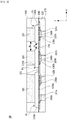
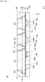
- a semiconductor device 1B according to the second embodiment may further include wavelength conversion layers 181, 182, and 183 and partitions 190 disposed on first to third light-emitting parts P1, P2, and P3.
- the wavelength conversion layers 181, 182, and 183 may convert wavelengths of light emitted from the first to third light-emitting parts P1, P2, and P3.
- a first wavelength conversion layer 181 may convert light emitted from the first light-emitting part P1 into green light
- a second wavelength conversion layer 182 may convert light emitted from the second light-emitting part P2 into red light
- a third wavelength conversion layer 183 may convert light emitted from the third light-emitting part P3 into blue light.
- the third wavelength conversion layer 183 may not change the wavelength or may not be disposed.
- the present invention is not necessarily limited thereto, and the first to third wavelength conversion layers 181, 182, and 183 may absorb light of a blue (B) wavelength band emitted from the first to third light-emitting parts P1, P2, and P3 and convert the light into light of a white (W) wavelength band.
- B blue
- W white
- the wavelength conversion layers 181, 182, and 183 may have a structure in which wavelength conversion particles are dispersed in a polymer resin selected from an epoxy resin, a silicone resin, a polyimide resin, a urea resin, an acrylic resin, and the like, but the present invention is not limited thereto.
- the wavelength conversion particles may include at least one of a phosphor and a quantum dot (QD).
- QD quantum dot
- the phosphor may include one fluorescent material among a YAG-based fluorescent material, a TAG-based fluorescent material, a silicate-based fluorescent material, a sulfide-based fluorescent material, and a nitride-based fluorescent material, but the embodiment is not limited to the type of the phosphor.
- the YAG-based and TAG-based fluorescent materials may be selected from among (Y, Tb, Lu, Sc, La, Gd, Sm) 3 (Al, Ga, In, Si, Fe) 5 (O, S) 12 :Ce, and the silicate-based fluorescent material may be selected from among (Sr, Ba, Ca, Mg) 2 SiO 4 :(Eu, F, Cl).
- the sulfide-based fluorescent material may be selected from among (Ca, Sr) S: Eu and (Sr,Ca,Ba)(Al,Ga) 2 S 4 :Eu
- the nitride-based phosphor may be (Sr, Ca, Si, Al, O)N:Eu (for example, CaAlSiN 4 :Eu ⁇ -SiAlON:Eu) or (Cax,My)(Si,Al) 12 (O,N) 16 which is a Ca- ⁇ SiAlON:Eu-based phosphor.
- M is at least one material among Eu, Tb, Yb, and Er, and may be selected from among phosphor components satisfying 0.05 ⁇ (x+y) ⁇ 0.3, 0.02 ⁇ x ⁇ 0.27, and 0.03 ⁇ y ⁇ 0.3.
- the wavelength conversion layers 181, 182, and 183 described above may be separated into regions overlapping the first to third light-emitting parts P1, P2, and P3 in a vertical direction by the partitions 190.
- the partitions 190 may be disposed between the wavelength conversion layers 181, 182, and 183 and between the light-emitting parts P1, P2, and P3.
- the partition 190 may include a light absorbing material such as carbon black or graphite, but may also include a reflective material that reflects the light.
- the partition 190 may have a structure in which reflective particles are dispersed in a base material.
- the base material may be at least one of an epoxy resin, a silicone resin, a polyimide resin, a urea resin, and an acrylic resin.
- the polymer resin may be a silicone resin.
- the reflective particles may include inorganic particles such as TiO 2 or SiO 2 , but the present invention is not limited thereto.
- the partition 190 may include 20 wt% or more of the inorganic particles.
- the inorganic particles in the partition may be in a range of 20 wt% to 70 wt%.
- reflectance of the partition 190 is lowered and thus color purity is lowered.
- the partition 190 when only the first light-emitting part P1 is turned on to emit green light, a portion of the light emitted from the first light-emitting part P1 may pass through the partition 190 and may be converted into red light by the second wavelength conversion layer 182. As a result, the color purity may be lowered.
- the partition 190 when the inorganic particles are more than 70 wt%, the content of the polymer resin becomes small, and thus cracks may occur.
- the partition 190 may include a first region disposed between the wavelength conversion layers 181, 182, and 183 and a second region disposed between the first to third light-emitting parts P1, P2, and P3.
- a width d1 of the first region may be greater than a width d2 of the second region.
- the present invention is not necessarily limited thereto, and the width d1 of the first region and the width d2 of the second region may be the same.
- the widths d1 and d2 of the first and second regions may be distances in a direction (an X axis direction) perpendicular to a thickness direction of the plurality of light emitting parts P1, P2, and P3.
- the width d1 of the first region of the partition 190 may be 10 ⁇ m or more.
- the width d1 of the first region may be in a range of 10 ⁇ m to 50 ⁇ m.
- the partition 190 may block the light emitted from the first to third light-emitting parts P1, P2, and P3 to improve color purity.
- the partition 190 blocks the light emitted from the first to third light-emitting parts P1, P2, and P3 to prevent color mixing and superposition of the light.
- the width d1 of the first region is greater than 50 ⁇ m, widths between first to third light-emitting parts P1, P2, and P3 are widened, and thus the size of the semiconductor device may be increased.
- the method of forming the partition 190 is not particularly limited.
- the partition 190 may be formed using photolithography, imprinting, roll-to-roll printing, and ink-jet printing, or the like.
- the width d1 of the first region may be greater than the maximum width d2 of the second region. Accordingly, the widths of the first to third wavelength conversion layers 181, 182, and 183 in the X axis direction may be smaller than the widths of the first to third light-emitting parts P1, P2, and P3, respectively. With such a structure, the width d1 of the partition may be increased while manufacturing the semiconductor device to have the same size. As an example, the width of each of the first to third wavelength conversion layers 181, 182, and 183 in the X axis direction may be 80% to 90% of the width of each of the first to third light-emitting parts P1, P2, and P3, respectively.
- the color purity was improved by 102% when the width of the first region was 20 ⁇ m
- the color purity was improved by 105% when the width of the first region was 30 ⁇ m
- the color purity was improved by 106% when the width of the first region was 50 ⁇ m.
- FIG. 5 is a cross-sectional view of a semiconductor device according to a third embodiment of the present invention
- FIG. 6 is a modified example of FIG. 5 .
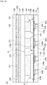
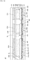
- a semiconductor device 1C may include a color filter layer 220 disposed above wavelength conversion layers 181, 182, and 183 and partitions 190
- the color filter layer 220 may include a plurality of color filters 221, 222, and 223 and a black matrix 224.
- First to third color filters 221, 222, and 223 may be disposed in the color filter layer 220.
- the first color filter 221 may be a green filter
- the second color filter 222 may be a red filter
- the third color filter 223 may be a blue filter.
- the plurality of color filters 221, 222, and 223 may be formed by mixing green/red/blue pigments with an acryl-based resin such as methylmethacrylate-butadiene-styrene (MBS).
- MBS methylmethacrylate-butadiene-styrene
- the color filter layer 220 may be formed by coating, exposing, developing, and curing (firing) a pigment composition dispersed in a photoresist.
- the color filter layer 220 may improve the color purity of light converted by the wavelength conversion layers 181, 182, and 183.
- the first color filter 221 may block light other than green light converted by a first wavelength conversion layer 181 to improve the color purity of the green light.
- the color filter layer 220 may separate light of a white (W) wavelength band into light of blue (B), green (G), and red (R) wavelength bands.
- the color filter layer 220 may include the black matrix 224 disposed between the first to third color filters 221, 222, and 223.
- the present invention is not necessarily limited thereto and a structure is not particularly limited as long as it is a structure that may be disposed and partitioned between the first to third color filters 221, 222, and 223.
- a thickness of the black matrix 224 may be in a range of 5 ⁇ m to 55 ⁇ m.
- the first to third color filters 221, 222, and 223 may not be partitioned due to a thickness that is too thin, and when the thickness is greater than 55 ⁇ m, there is a problem in that the entire thickness of the filter becomes thick.
- the thickness of the black matrix 224 is not necessarily limited thereto.
- a width of the black matrix 224 may be in a range of +/- 5 ⁇ m of a width d1 of a first region of the partition 190 disposed below the black matrix 224.
- the width of the black matrix 224 may be in a range of 5 ⁇ m to 55 ⁇ m.
- a first intermediate layer 210 may be disposed between the color filter layer 220 and the wavelength conversion layers 181, 182, and 183 to perform the role of adhering them.
- the color filters 221, 222, and 223 may use an acrylic resin as a main raw material
- the partitions and the wavelength conversion layers 181, 182, and 183 may use a silicone resin as a main raw material.
- the acrylic resin and the silicone resin have a poor adhesive property due to differences in physical properties, it may not be easy to form the color filters 221, 222, and 223 directly on the wavelength conversion layers 181, 182, and 183.
- the first intermediate layer 210 may include an oxide or a nitride as an inorganic material.
- the first intermediate layer 210 may be formed as a single layer or a multilayer including at least one of indium tin oxide (ITO), indium zinc oxide (IZO), indium zinc tin oxide (IZTO), indium aluminum zinc oxide (IAZO), indium gallium zinc oxide (IGZO), indium gallium tin oxide (IGTO), aluminum zinc oxide (AZO), antimony tin oxide (ATO), gallium zinc oxide (GZO), IZO Nitride (IZON), Al-Ga ZnO (AGZO), In-Ga ZnO (IGZO), ZnO, IrOx, RuOx, NiO, RuOx/ITO, ZnO, SiO 2 , Si x O y , Si 3 N 4 , Si x N y , SiO x N y , Al 2 O 3 , TiO 2 , and AlN.
- a thickness of the first intermediate layer 210 may be in a range of 5 nm to 1,000 nm, or 40 nm to 200 nm. When the thickness is less than 5 nm, it is difficult to prevent the acrylic resin from diffusing into a phosphor, and when the thickness is more than 1000 nm, there is a problem in that transmittance becomes smaller than 70%, leading to a decrease in luminous flux.
- a total thickness L 1 of the partition 190, the first intermediate layer 210, the color filter layer 220, and an encapsulation layer 230 may be in a range of 30 ⁇ m to 100 ⁇ m.
- the total thickness L 1 of the partition 190, the first intermediate layer 210, the color filter layer 220, and the encapsulation layer 230 is less than 30 ⁇ m, the number of particles in the wavelength conversion layers 181, 182, and 183 is small, such that color conversion may be reduced and the process may be difficult.
- the total thickness L 1 of the partition 190, the first intermediate layer 210, the color filter layer 220, and the encapsulation layer 230 is greater than 100 ⁇ m, the light transmittance may be reduced due to the thickness.
- the thickness denotes a distance in a Y-axis direction.
- a second intermediate layer 240 may be disposed between a first intermediate layer 210 and wavelength conversion layers 181, 182, and 183.
- the wavelength conversion layers 181, 182, and 183 may not have a flat surface due to a process or the dispersion of phosphor particles in a resin. Accordingly, when a color filter layer is formed on surfaces of the wavelength conversion layers 181, 182, and 183, there is a problem that reliability is lowered.
- the first intermediate layer 210 may be disposed on the second intermediate layer 240 to provide the flat surface.
- the present invention is not necessarily limited thereto, and the configuration of the second intermediate layer 240 may be omitted.
- the second intermediate layer 240 may be omitted.
- the surface roughness of the first intermediate layer 210 may be determined by the surface roughness of the wavelength conversion layers 181, 182, and 183 and the partitions 190.
- a leveling or polishing process may be performed to control the surface roughness of the wavelength conversion layers 181, 182, and 183 and the partitions 190.
- the second intermediate layer 240 may include the same material as the wavelength conversion layers 181, 182, and 183 for adhesion therewith.
- both the second intermediate layer 240 and the wavelength conversion layers 181, 182, and 183 may include a silicone resin.
- a thickness of the second intermediate layer 240 may be in a range of 3,000 nm to 20,000 nm. When the thickness of the second intermediate layer 240 is less than 3,000 nm, the surface planarization of the second intermediate layer 240 may be poor, and when the thickness is greater than 20,000 nm, light transmittance is decreased. Thus, a thickness ratio of the first intermediate layer 210 to the second intermediate layer 240 may be in a range of 1:4000 to 1:3.
- An encapsulation layer 230 may be disposed on a color filter layer 220.
- the encapsulation layer 230 may protect a plurality of light emitting parts P1, P2, and P3, the wavelength conversion layers 181, 182, and 183, and the partitions 190 by being disposed on the color filter layer 220 so as to cover pixels and the semiconductor device.
- the encapsulation layer 230 is made of a heat- and/or light-curable resin and coated on the color filter layer 220 in a liquid state, and may be cured by a curing process using heat and/or light.
- the encapsulation layer 230 may also serve to buffer external pressing.
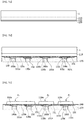
- FIGS. 7A to 7F are views illustrating a method of manufacturing the semiconductor device according to the third embodiment.
- a first conductive type semiconductor layer 110, an active layer 120, and a second conductive type semiconductor layer 130 may be sequentially formed on a substrate 1.
- the substrate 1 may be formed of a material selected from the group consisting of sapphire (Al 2 O 3 ), SiC, GaAs, GaN, ZnO, Si, GaP, InP, and Ge, but the present invention is not limited thereto.
- a buffer layer (not shown) may be further provided between the first conductive type semiconductor layer 110 and the substrate 1.
- the buffer layer may mitigate a lattice mismatch between the first conductive type semiconductor layer 110, the active layer 120, and the second conductive type semiconductor layer 130, and the substrate 1.
- the buffer layer may include a combination of a Group III element and a Group V element or any one selected from the group consisting of GaN, InN, AlN, InGaN, AlGaN, InAlGaN, and AlInN.
- the buffer layer may be doped with a dopant, but the present invention is not limited thereto.
- the first conductive type semiconductor layer 110, the active layer 120, and the second conductive type semiconductor layer 130 may be formed by a method such as a metal organic chemical vapor deposition (MOCVD) method, a chemical vapor deposition (CVD) method, a plasma-enhanced chemical vapor deposition (PECVD) method, a molecular beam epitaxy (MBE) method, a hydride vapor phase epitaxy (HVPE) method, or a sputtering method, but the present invention is not limited thereto.
- MOCVD metal organic chemical vapor deposition
- CVD chemical vapor deposition
- PECVD plasma-enhanced chemical vapor deposition
- MBE molecular beam epitaxy
- HVPE hydride vapor phase epitaxy
- a first insulating layer 140, a first electrode 151, and second electrodes 161a, 161b, and 161c may be formed on the second conductive type semiconductor layer 130. Subsequently, a support layer 170 is formed, and then a first bump electrode 150 and second bump electrodes 160a, 160b, and 160c may be formed to pass through the support layer 170.
- the present invention is not limited thereto, and the first bump electrode 150 and the second bump electrodes 160a, 160b, and 160c may be formed, and then the support layer 170 may be formed.
- second conductive type semiconductor layers 130a, 130b, and 130c and active layers 120a, 120b, and 120c may be mesa-etched and separated from each other. Accordingly, the second conductivity type semiconductor layers 130a, 130b, and 130c and the active layers 120a, 120b, and 120c may be formed to narrow in width in a direction away from the substrate 1.
- the substrate 1 may be removed.
- the substrate 1 may be removed using a laser lift off (LLO) method, but the present invention is not limited thereto.
- LLO laser lift off
- the first conductive type semiconductor layer 110 may be separated into each part unit of the light-emitting parts P1, P2, and P3. Accordingly, the first conductive type semiconductor layer 110 may be formed to have a smaller width in a direction opposite to the second conductive type semiconductor layer 130 during a mesa etching process.
- wavelength conversion layers 181, 182, and 183 and partitions 190 may be formed on the first conductive type semiconductor layer 110.
- the wavelength conversion layers 181, 182, and 183 may be formed first, and then the partitions 190 may be formed, but the present invention is not necessarily limited thereto, and the partitions 190 may be formed first to form through holes, and the wavelength conversion layers 181, 182, and 183 may be formed in the through holes.
- a first intermediate layer 210 may be formed on the wavelength conversion layers 181, 182, and 183, and then first to third color filters 221, 222, and 223 may be formed on the first intermediate layer 210.
- black matrix may be formed first and aligned with the wavelength conversion layers 181, 182, and 183, and then the first to third color filters 221, 222, and 223 may be formed after, but the present invention is not limited thereto.
- the first color filter 221 may be formed on a region corresponding to the first wavelength conversion layer 181 by applying a green pigment over the entire surface by a method such as spin coating or bar coating, and performing a mask process.
- the second color filter 222 may be formed on a region corresponding to the second wavelength conversion layer 182 by applying a red pigment over the entire surface by a method such as spin coating or bar coating, and performing a mask process.
- the third color filter 223 may be formed on a region corresponding to the third wavelength conversion layer 183 by applying a blue pigment over the entire surface by a method such as spin coating or bar coating, and performing a mask process.
- an encapsulation layer 230 may be formed on the color filter layer 220 as shown in FIG. 7F .
- FIG. 8 is a cross-sectional view of a semiconductor device according to a fourth embodiment of the present invention.
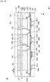
- a semiconductor device 1D may further include a blocking layer 200 disposed between wavelength conversion layers 181, 182, and 183 and between first to third light-emitting parts P1, P2, and P3.
- the blocking layer 200 may also be disposed on a first insulating layer 140.
- the blocking layer 200 may block the emission of light emitted from the first to third light-emitting parts P1, P2, and P3 to the adjacent wavelength conversion layers 181, 182, and 183.
- the blocking layer 200 may prevent the light emitted from the first light-emitting part P1 from being incident on the second wavelength conversion layer 182. With such a configuration, the blocking layer 200 may prevent color mixing and superposition of the light.
- the blocking layer 200 may include a metal.
- the blocking layer 200 may include a light reflective metal to reflect the light traveling to the adjacent wavelength conversion layers 181, 182, and 183.
- the metal may include, but is not limited to, Ag, Ni, Ti, or Al.
- a width d3 of the blocking layer 200 may be 20 nm or more, and preferably, the width d3 of the blocking layer 200 may be in a range of 100 nm to 1000 nm.
- the width d3 of the blocking layer 200 is less than 100 nm, it is difficult to fix the blocking layer 200, and thus the surface roughness may be increased.
- the width d3 of the blocking layer 200 is greater than 1000 nm, peeling may occur due to stress caused by weight or the like.
- the blocking layer 200 may be formed by the deposition of a metal, but the present invention is not limited thereto.
- the color filter layer 220 may include a plurality of color filters 221, 222, and 223 and black matrix 224.
- First to third color filters 221, 222, and 223 may be disposed in the color filter layer 220.
- the first color filter 221 may be a green filter
- the second color filter 222 may be a red filter
- the third color filter 223 may be a blue filter.
- a first intermediate layer 210 may be disposed between the color filter layer 220 and the wavelength conversion layers 181, 182, and 183 to perform the role of adhering them.
- the features described in FIG. 5 may be applied as they are to the color filter layer 220 and the first intermediate layer 210. Further, the second intermediate layer of FIG. 6 may be further disposed.
- FIGS. 9A to 9D are views illustrating a method of manufacturing the semiconductor device according to the fourth embodiment.
- the manufacturing process described with reference to FIGS. 7A to 7C may be applied as it is to the light-emitting device according to FIG. 9A . That is, after removing a substrate, a first conductive type semiconductor layer 110 may be separated into each part unit of light-emitting parts P1, P2, and P3. Accordingly, the first conductive type semiconductor layer 110 may be formed to have a smaller width in a direction opposite to a second conductive type semiconductor layer 130 during a mesa etching process.
- wavelength conversion layers 181, 182, and 183 and photosensitive layers S may be formed on the first conductive type semiconductor layer 110.
- the wavelength conversion layers 181, 182, and 183 may be formed first, and then the photosensitive layers S may be formed, but the present invention is not necessarily limited thereto, and the photosensitive layers S are formed first to form through holes and the wavelength conversion layers 181, 182, and 183 may be formed in the through holes.
- a blocking layer 200 may be formed between the wavelength conversion layers 181, 182, and 183, the first to third light-emitting parts P1, P2, and P3, and a first electrode 151, and partitions 190.
- the blocking layer 200 may be deposited after removing the photosensitive layers S.
- the blocking layer 200 may be formed using methods such as a metal organic chemical vapor deposition (MOCVD) method, a chemical vapor deposition (CVD) method, a sputtering method, or the like, but the present invention is not limited thereto.
- MOCVD metal organic chemical vapor deposition
- CVD chemical vapor deposition
- sputtering method or the like
- the blocking layer 200 may be formed, and then the partition 190 may be formed on the blocking layer 200.
- parts of the wavelength conversion layers 181, 182, and 183, the partitions 190, and the blocking layer 200 may be removed such that an upper surface of each of the wavelength conversion layers 181, 182, and 183, the partitions 190, and the blocking layer 200 is exposed.
- a leveling or polishing process may be applied to the removing method, but the present invention is not necessarily limited thereto.
- FIG. 10 is a cross-sectional view of a modified example of the semiconductor device according to the fourth embodiment shown in FIG. 8 .
- a blocking layer 200 of a semiconductor device ID' is formed between wavelength conversion layers 181, 182, and 183 and first to third light-emitting parts P1, P2, and P3, and partitions 190.
- a first insulating layer 140 may be exposed through the blocking layer 200.
- the blocking layer 200 may block the emission of light emitted from the first to third light-emitting parts P1, P2, and P3 to the adjacent wavelength conversion layers 181, 182, and 183. With such a configuration, the blocking layer 200 may prevent color mixing and superposition of the light. The above description may be equally applied to the blocking layers 200
- FIG. 11 is a cross-sectional view of a semiconductor device according to a fifth embodiment of the present invention.
- a semiconductor device 1E may include first to third light-emitting parts P1, P2, and P3, first bump electrodes 150a, 150b, and 150c electrically connected to first conductive type semiconductor layers 110a, 110b, and 110c spaced apart from each other, respectively, a second electrode 162 electrically connecting separated second conductive type semiconductor layers 130a, 130b, and 130c, and a second bump electrode 160 electrically connected to the second electrode 162.
- the first bump electrodes 150a, 150b, and 150c are electrically connected to the first conductive type semiconductor layers 110a, 110b, and 110c, respectively, and the second bump electrode 160 may be electrically connected to the second conductive type semiconductor layers 130a, 130b, and 130c through the second electrode 162.
- the second electrode 162 may be disposed between the second conductive type semiconductor layers 130a, 130b, and 130c spaced apart from each other in the first to third light-emitting parts P1, P2, and P3. Further, the second electrode 162 may electrically connect the separated second conductive type semiconductor layers 130a, 130b, and 130c to each other.
- a first insulating layer 140 may be disposed below the first to third light-emitting parts P1, P2, and P3.
- reflective electrodes 161 may be disposed below the second conductive type semiconductor layers 130a, 130b, and 130c.
- first electrodes 151a, 151b, and 151c may be disposed between the first conductive type semiconductor layers 110a, 110b, and 110c of the first to third light-emitting parts P1, P2, and P3, and the first bump electrodes 150a, 150b, and 150c, respectively.
- the reflective electrode 161 may be formed of a material having a high reflectance such as Ag, Ni, Al, Rh, Pd, Ir, Ru, Mg, Zn, Pt, Au, or Hf, or may be formed as a single layer or a multilayer by mixing the material having a high reflectance and a conductive material such as IZO, IZTO, IAZO, IGZO, IGTO, AZO, or ATO, but the present invention is not limited thereto.
- a material having a high reflectance such as Ag, Ni, Al, Rh, Pd, Ir, Ru, Mg, Zn, Pt, Au, or Hf
- a conductive material such as IZO, IZTO, IAZO, IGZO, IGTO, AZO, or ATO, but the present invention is not limited thereto.
- the second electrode 162 may be disposed between the reflective electrodes 161 to electrically connect the second conductive type semiconductor layers 130a, 130b, and 130c to the second bump electrode 160.
- the second electrode 162 may serve as a common electrode configured to apply power to the first to third light-emitting parts P1, P2, and P3.
- the first insulating layer 140 may be disposed to cover lower portions of the first to third light-emitting parts P1, P2, and P3.
- a second insulating layer 141 may cover a part of the first electrodes 151a, 151b, and 151c, a part of the reflective electrodes 161, and the entire second electrode 162.
- the first insulating layer 140 and the second insulating layer 141 may be formed of at least one selected from the group consisting of SiO 2 , Si x O y , Si 3 N 4 , Si x N y , SiO x N y , Al 2 O 3 , TiO 2 , AlN, and the like, but the present invention is not limited thereto.
- the first insulating layer 140 may be a DBR having a multi-layer structure including a Si oxide or a Ti compound. However, the present invention is not necessarily limited thereto, and the first insulating layer 140 may include various reflection structures.
- a support layer 170 may be disposed below the plurality of light emitting parts P1, P2, and P3 to support the plurality of light emitting parts P1, P2, and P3 and the second electrode 162. Further, the support layer 170 has low light transmittance and may function as a light reflective layer and/or a light absorption layer.
- the support layer 170 may have a structure in which reflective particles are dispersed in a base material.
- the base material may be at least one of a light-transmitting epoxy resin, a silicone resin, a polyimide resin, a urea resin, and an acrylic resin.
- a polymer resin may be a silicone resin.
- the reflective particles may include inorganic particles such as TiO 2 or SiO 2 .
- the present invention is not necessarily limited thereto, and the support layer may be an EMC resin or an SMC resin.
- the support layer 170 may include 10 to 50 wt%, or 15 to 30 wt% of inorganic particles. When the content of the particles is less than 10 wt%, it is difficult to control the transmittance to 20% or less, and when the content is greater than 50 wt%, the content of the inorganic particles is great, and thus cracks may occur.
- the support layer 170 may have a CTE of 50 ppm/°C or less. Accordingly, when the thickness of the support layer 170 is 70 ⁇ m or more, the transmittance of the support layer 170 may be 20 % or less. As a result, light generated in the first to third light-emitting parts P1, P2, and P3 may be reflected at the support layer 170 toward upper portions of the first conductive type semiconductor layers 110a, 110b, and 110c. Thus, the semiconductor device according to one embodiment may provide improved light emission efficiency.
- the first bump electrodes 150a, 150b, and 150c may be electrically connected to the first electrodes 151a, 151b, and 151c through the support layer 170.
- the second bump electrode 160 may be electrically connected to the reflective electrode 161 through the support layer 170.
- the reflective electrodes 161 may be electrically connected to each other by the second electrode 162.
- the present invention is not limited thereto.
- the second bump electrode 160 may be electrically connected to the second conductive type semiconductor layers 130a, 130b, and 130c of the first to third light-emitting parts P1, P2, and P3 through the reflective electrodes 161 and the second electrode 162.
- FIG. 12 is a cross-sectional view of a semiconductor device according to a sixth embodiment of the present invention
- FIG. 13 is a cross-sectional view of a semiconductor device according to a seventh embodiment of the present invention.
- a semiconductor device 1F may further include wavelength conversion layers 181, 182, and 183 and partitions 190 disposed on first to third light-emitting parts P1, P2, and P3.
- the wavelength conversion layers 181, 182, and 183 may convert the wavelengths of light emitted from the first to third light-emitting parts P1, P2, and P3.
- a first wavelength conversion layer 181 may convert light emitted from the first light-emitting part P1 into green light
- a second wavelength conversion layer 182 may convert light emitted from the second light-emitting part P2 into red light
- a third wavelength conversion layer 183 may convert light emitted from the third light-emitting part P3 into blue light.
- the third wavelength conversion layer 183 may not change the wavelength.
- the present invention is not necessarily limited thereto, and the first to third wavelength conversion layers 181, 182, and 183 may absorb light of a blue (B) wavelength band emitted from the first to third light-emitting parts P1, P2, and P3 and convert the light into light of a white (W) wavelength band.
- B blue
- W white
- the wavelength conversion layers 181, 182, and 183 may have a structure in which wavelength conversion particles are dispersed in a polymer resin selected from a transmitting epoxy resin, a silicone resin, a polyimide resin, a urea resin, an acrylic resin, and the like, but the present invention is not limited thereto.
- the wavelength conversion particles may include at least one of a phosphor and a QD.
- the wavelength conversion particles will be described as a phosphor.
- the phosphor may include one fluorescent material among a YAG-based fluorescent material, a TAG-based fluorescent material, a silicate-based fluorescent material, a sulfide-based fluorescent material, and a nitride-based fluorescent material, but the embodiment is not limited to the type of the phosphor.
- the YAG-based and TAG-based fluorescent materials may be selected from among (Y, Tb, Lu, Sc, La, Gd, Sm) 3 (Al, Ga, In, Si, Fe) 5 (O, S) 12 :Ce, and the silicate-based fluorescent material may be selected from among (Sr, Ba, Ca, Mg) 2 SiO 4 :(Eu, F, Cl).
- the sulfide-based fluorescent material may be selected from among (Ca, Sr) S: Eu and (Sr,Ca,Ba)(Al,Ga) 2 S 4 :Eu
- the nitride-based phosphor may be (Sr, Ca, Si, Al, O)N:Eu (for example, CaAlSiN 4 :Eu ⁇ -SiAlON:Eu) or (Cax,My)(Si,Al) 12 (O,N) 16 which is a Ca- ⁇ SiAlON:Eu-based phosphor.
- M is at least one material among Eu, Tb, Yb, and Er, and may be selected from among phosphor components satisfying 0.05 ⁇ (x+y) ⁇ 0.3, 0.02 ⁇ x ⁇ 0.27 and 0.03 ⁇ y ⁇ 0.3.
- the wavelength conversion layers 181, 182, and 183 described above may be separated into regions overlapping the first to third light-emitting parts P1, P2, and P3 in a vertical direction by the partitions 190.
- the partitions 190 may be disposed between the wavelength conversion layers 181, 182, and 183 and between the light-emitting parts P1, P2, and P3.
- the partitions 190 may include a light absorbing material such as carbon black or graphite, but may also include a reflective material that reflects the light.
- the partition 190 may be a structure in which reflective particles are dispersed in a base material.
- the base material may be at least one of an epoxy resin, a silicone resin, a polyimide resin, a urea resin, and an acrylic resin.
- the polymer resin may be a silicone resin.
- the reflective particles may include inorganic particles such as TiO 2 or SiO 2 , but the present invention is not limited thereto.
- the partition 190 may include 20 wt% or more of the inorganic particles.
- the inorganic particles in the partition may be in a range of 20 wt% to 70 wt%.
- reflectance of the partition 190 is lowered and thus color purity is lowered.
- the inorganic particles exceed 70 wt%, cracks may occur in the partition 190.
- the partition 190 may include a first region disposed between the wavelength conversion layers 181, 182, and 183 and a second region disposed between the first to third light-emitting parts P1, P2, and P3.
- the description of the partition 190 may be applied in the same manner as described above.
- a semiconductor device 1G may include a color filter layer 220 disposed above wavelength conversion layers 181, 182, and 183 and partition 190
- First to third color filters 221, 222, and 223 may be disposed in the color filter layer 220.
- the first color filter 221 may be a green filter
- the second color filter 222 may be a red filter
- the third color filter 223 may be a blue filter.
- the color filter layer 220 may be formed by mixing green/red/blue pigments with an acrylic resin such as methylmethacrylate-butadiene-styrene (MBS).
- MBS methylmethacrylate-butadiene-styrene
- the color filter layer 220 may be formed by coating, exposing, developing, and curing (firing) a pigment composition dispersed in a photoresist.
- the color filter layer 220 may improve the color purity of light converted by the wavelength conversion layers 181, 182, and 183.
- the first color filter 221 may block light other than green light converted by a first wavelength conversion layer 181 to improve the color purity of the green light.
- the color filter layer 220 may separate light of a white (W) wavelength band into light of blue (B), green (G), and red (R) wavelength bands.
- the color filter layer 220 may include black matrix 224 disposed between the first to third color filters 221, 222, and 223.
- a first intermediate layer 210 may be disposed between the color filter layer 220 and the wavelength conversion layers 181, 182, and 183.
- the color filter layer 220 may use an acrylic resin as a main raw material
- the partitions and the wavelength conversion layers 181, 182, and 183 may use a silicone resin as a main raw material.
- the acrylic resin and the silicone resin have a poor adhesive property, it may not be easy to form the color filter layer 220 directly on the wavelength conversion layers 181, 182, and 183.
- the first intermediate layer 210 may include an oxide or a nitride as an inorganic material.
- the first intermediate layer 210 may include ITO, ZnO, AZO, or SiO 2 .
- the present invention is not necessarily limited thereto, and any material having excellent adhesion to both the acrylic resin and the silicone resin may be selected for the first intermediate layer 210.
- a thickness of the first intermediate layer 210 may be in a range of 5 nm to 1000 nm, or 40 nm to 200 nm. When the thickness is less than 5 nm, it is difficult to prevent the acrylic resin from diffusing into a phosphor, and when the thickness is more than 1000 nm, there is a problem in that transmittance becomes smaller than 70% and thus luminous flux decreases.
- a second intermediate layer may be disposed between the first intermediate layer 210 and the wavelength conversion layers 181, 182, and 183.
- An encapsulation layer 230 may be disposed on the color filter layer 220.
- the encapsulation layer 230 may protect the plurality of light emitting parts P1, P2, and P3, the wavelength conversion layers 181, 182, and 183, and the partitions 190 by being disposed on the color filter layer 220 so as to cover pixels and the semiconductor device.
- the encapsulation layer 230 is made of a heat- and/or light-curable resin and coated on the color filter layer 220 in a liquid state, and may be cured by a curing process using heat and/or light.
- the encapsulation layer 230 also serves to buffer external pressing.
- FIG. 14 is a plan view of a display device according to one embodiment of the present invention
- FIG. 15 is a view illustrating a state in which a semiconductor device and a circuit board are electrically connected to each other.
- the display device may include a panel 40 having a plurality of pixel regions defined as regions in which common wirings 41 intersect driving wirings 42, semiconductor devices disposed in each pixel region, a first driver 30 configured to apply driving signals to the common wirings 41, a second driver 20 configured to apply driving signals to the driving wirings 42, and a controller 50 configured to control the first driver 30 and the second driver 20.
- Second partitions 46 disposed on the panel 40 are disposed between the semiconductor devices disposed in each pixel region to support the semiconductor devices, the common wirings 41, the driving wirings 42, and the like. Thus, even when the panel 40 is enlarged to have a large area, disconnection of the common wiring 41 and the driving wiring 42 may be prevented.
- the second partitions 46 may be formed of a material such as carbon black, graphite, and the like to prevent light leakage between adjacent pixel regions, but the present invention is not limited thereto.
- the common wiring 41 may be electrically connected to a first electrode 150 of the semiconductor device.
- first, second, and third driving wirings 43, 44, and 45 may be electrically connected to second electrodes 160a, 160b, and 160c of first, second, and third light-emitting parts P1, P2, and P3, respectively.
- the common wiring 41 and the driving wiring 42 may have a structure separated from each other with at least one insulating film interposed therebetween, but the present invention is not limited thereto.
- first and second insulating films 1a and 1b are illustrated.
- the semiconductor device may be disposed for each pixel region of the panel 40.
- One semiconductor device may function as a pixel of the display device.
- the first to third light-emitting parts P1, P2, and P3 of the semiconductor device may function as first, second, and third subpixels.
- the first light-emitting part P1 may function as a blue subpixel
- the second light-emitting part P2 may function as a green subpixel
- the third light-emitting part P3 may function as a red subpixel. Accordingly, white light may be realized by mixing light of blue, green, and red wavelength bands emitted from one semiconductor device.
- the semiconductor devices may be disposed on a substrate in a chip scale package (CSP).
- CSP chip scale package
- the controller 50 may output control signals to the first and second drivers 30 and 20 such that power is selectively applied to the common wirings 41 and the driving wirings 42. Accordingly, the first to third light-emitting parts P1, P2, and P3 of the semiconductor device may be controlled individually.
- light-emitting devices may be individually disposed on each subpixel of a pixel, or a semiconductor device including two or more light-emitting devices packaged through an additional packaging process such as die bonding and wire bonding may be disposed on a pixel. Accordingly, since a packaging area should be taken into consideration in the typical display device, the area of the actual light-emitting region of the entire area of a panel becomes narrow, and light emission efficiency is low.
- a chip-level semiconductor device is disposed in the pixel region, and the first, second, and third light-emitting parts P1, P2, and P3 of the semiconductor device may function as first to third subpixels of R, G, and B.
- the first, second, and third light-emitting parts P1, P2, and P3 of the semiconductor device may function as first to third subpixels of R, G, and B.
- the semiconductor device of the embodiments does not need to secure the above-described bonding regions. Accordingly, the light emission efficiency may be high, and the widths between the first to third light-emitting parts P1, P2, and P3 are reduced as described above, and thus the size of the semiconductor device may be reduced.
- SD standard definition
- HD high definition
- FHD full HD
- UH ultra HD
- the display device of the embodiments may also be applied to an electric signboard or TV with a diagonal size of 100 inches or more. This is because, as described above, the semiconductor device according to the embodiments functions as each pixel and thus may have low power consumption and a long lifespan, with low maintenance costs.
Landscapes
- Led Devices (AREA)
- Led Device Packages (AREA)
Abstract
Description
- Embodiments relate to a semiconductor device and a display device including the same.
- A light-emitting diode (LED) is one of light-emitting devices that emit light when current is applied. The LED may emit high-efficiency light at a low voltage and thus has an excellent energy saving effect. Recently, since the luminance problem of the LED has been significantly improved, LEDs are being applied to various devices such as backlight units of liquid crystal display devices, electric signboards, indicators, and home appliances.
- A typical liquid crystal display device controls light emitted from a light-emitting diode and the transmittance of a liquid crystal to display images or pictures with light passing through a color filter. Recently, although there has been a need for a display device having high definition and a large-screen, liquid crystal display devices and organic light-emitting display devices, which have complex configurations and are most commonly used, have difficulty in realizing high-definition, large-screen display devices due to yield and cost.
- Embodiments provide a semiconductor device with improved color purity.
- Also, embodiments provide a semiconductor device with improved luminous intensity.
- In the embodiments, a chip level light-emitting device including individually driven first to third light-emitting parts may be provided as a pixel of a display device. Here, the first to third light-emitting parts function as each subpixel of the pixel, and thus a large-sized display device of high resolution may be realized.
- Problems to be solved in the embodiments are not limited to the above-described problems, and objects and effects which may be grasped from the solution means, and the exemplary embodiments of the problems described below are also included.
- One aspect of the present invention provides a semiconductor device including a plurality of light-emitting parts, a plurality of wavelength conversion layers disposed on the plurality of light-emitting parts, respectively, partitions disposed between the plurality of light-emitting parts and between the plurality of wavelength conversion layers, a plurality of color filters disposed on the plurality of wavelength conversion layers, respectively, and black matrix disposed between the plurality of color filters.
- A width between the plurality of wavelength conversion layers may be greater than the maximum width between the plurality of light-emitting parts.
- Each of the light-emitting parts may include a first conductive type semiconductor layer, a second conductive type semiconductor layer, and an active layer disposed between the first conductive type semiconductor layer and the second conductive type semiconductor layer.
- The first conductive type semiconductor layer of the plurality of light-emitting parts may have a width that narrows toward the wavelength conversion layer.
- The second conductive type semiconductor layer of the plurality of light-emitting parts may have a width that increases toward the wavelength conversion layer.
- The semiconductor device may include a first bump electrode commonly connected to the plurality of light-emitting parts, a plurality of second bump electrodes electrically connected to the plurality of light-emitting parts, respectively, a first electrode electrically connecting the first conductive type semiconductor layers of the plurality of light-emitting parts to each other, and a first insulating layer covering lower portions of the plurality of light-emitting parts.
- The semiconductor device may further include a first insulating layer covering lower portions of the plurality of light-emitting parts.
- The first electrode may be electrically connected to the first conductive type semiconductor layer through the first insulating layer.
- The first electrode may be electrically connected to the first bump electrode.
- The semiconductor device may include a plurality of first bump electrodes electrically connected to the plurality of light-emitting parts, respectively, a second bump electrode commonly connected to the plurality of light-emitting parts, and a second electrode electrically connecting the second conductive type semiconductor layers of the plurality of light-emitting parts to each other.
- The second electrode may be electrically connected to the second bump electrode.
- The semiconductor device may further include a first insulating layer covering lower portions of the plurality of light-emitting parts.
- The semiconductor device may further include a plurality of reflective electrodes passing through the first insulating layer and disposed below the second conductive type semiconductor layers of the plurality of light-emitting parts, respectively, and the second electrode may electrically connect the plurality of reflective electrodes to each other.
- A width between the neighboring wavelength conversion layers may be in a range of 30 µm to 50 µm.
- The partitions may include reflective particles.
- The semiconductor device may further include a color filter layer disposed on the wavelength conversion layer, and the color filter layer may include the plurality of color filters and the black matrix.
- A display device according to one embodiment of the present invention may include the semiconductor device.
- The display device may include a panel having a plurality of pixel regions defined as regions in which common wirings intersect driving wirings, and the semiconductor device is disposed on each pixel region so that the first, second, and third light-emitting parts may be first, second, and third subpixels emitting light of green, red, and blue wavelength bands, respectively.
- In a semiconductor device of the embodiments, color purity can be improved.
- In a semiconductor device of the embodiments, relative luminous intensity can be improved.
- In a semiconductor device of the embodiments, a chip level light-emitting device including individually driven first to third light-emitting parts can be provided as a pixel of a display device. Here, the first to third light-emitting parts can function as each subpixel of the pixel, and a large-sized display device of a high-resolution can be realized.
- Various advantages and effects of the present invention are not limited to the above description and can be more easily understood through the description of specific exemplary embodiments of the present invention.
-
-
FIG. 1 is a plan view of a semiconductor device according to a first embodiment of the present invention. -
FIG. 2 is a cross-sectional view taken along line A-A inFIG. 1 . -
FIG. 3 is a cross-sectional view of a semiconductor device according to a second embodiment of the present invention. -
FIGS. 4A and 4B are graphs illustrating changes in luminous flux and color purity according to the width of a partition of the semiconductor device according to the embodiments. -
FIG. 5 is a cross-sectional view of a semiconductor device according to a third embodiment of the present invention. -
FIG. 6 is a modified example ofFIG. 5 . -
FIGS. 7A to 7F are views illustrating a method of manufacturing the semiconductor device according to the third embodiment. -
FIG. 8 is a cross-sectional view of a semiconductor device according to a fourth embodiment of the present invention. -
FIGS. 9A to 9D are views illustrating a method of manufacturing the semiconductor device according to the fourth embodiment. -
FIG. 10 is a cross-sectional view of a modified example of the semiconductor device according to the fourth embodiment shown inFIG. 8 . -
FIG. 11 is a cross-sectional view of a semiconductor device according to a fifth embodiment of the present invention. -
FIG. 12 is a cross-sectional view of a semiconductor device according to a sixth embodiment of the present invention. -
FIG. 13 is a cross-sectional view of a semiconductor device according to a seventh embodiment of the present invention. -
FIG. 14 is a plan view of a display device according to one embodiment of the present invention. -
FIG. 15 is a view illustrating a state in which a semiconductor device and a circuit board are electrically connected to each other. - The embodiments may be modified in other forms, or several embodiments may be combined with one another, and the scope of the present invention is not limited to each of the embodiments described below.
- Even when content described in a specific embodiment is not described in other embodiments, the content may be understood as being related to other embodiments unless described otherwise or the content contradicts a specific embodiment in the other embodiments.
- For example, when features of a component A are described in a specific embodiment and features of a component B are described in another embodiment, it should be understood that embodiments in which the component A is combined with the component B fall within the scope and spirit of the present invention even when they are not explicitly described, unless there is an opposite or contradictory explanation.
- In the description of the embodiments, when one element is referred to as being "on" or "under" another element, the term "on" or "under" refers to either a direct connection between two elements or an indirect connection between two elements having one or more elements formed therebetween. In addition, when the term "on" or "under" is used, it may refer to a downward direction as well as an upward direction with respect to an element.
- Hereinafter, embodiments of the present invention will be described in detail with reference to the accompanying drawings so that those of ordinary skill in the art can easily implement them.
- A semiconductor device may include various electronic devices such as a light-emitting device and a light-receiving device, and both the light-emitting device and the light-receiving device may include first conductive
type semiconductor layers active layers type semiconductor layers - The semiconductor device according to the present embodiment may be a light-emitting device.
- The light-emitting device emits light by the recombination of electrons and holes, and the wavelength of the light is determined by an inherent energy band gap of a material. Thus, the light emitted may vary depending on the composition of the material.
- Hereinafter, the semiconductor device of the embodiment will be described in detail with reference to the accompanying drawings.
-
FIG. 1 is a plan view of a semiconductor device according to a first embodiment of the present invention, andFIG. 2 is a cross-sectional view taken along line A-A inFIG. 2 . - Referring to
FIG. 1 , the semiconductor device may include a plurality of light emitting parts P1, P2, and P3. The plurality of light emitting parts P1, P2, and P3 may each emit light of the same wavelength or different wavelengths. The plurality of light emitting parts P1, P2, and P3 may be defined as regions that may be controlled independently from each other. As an example, only one of first to third light-emitting parts P1, P2, and P3 among the plurality of light emitting parts P1, P2, and P3 may be independently turned on by selectively applying current thereto. - The plurality of light emitting parts P1, P2, and P3 may include the first light-emitting part P1 configured to emit light of a first wavelength band, a second light-emitting part P2 configured to emit light of a second wavelength band, and a third light-emitting part P3 configured to emit light of a third wavelength band.
- The first light-emitting part P1 may emit green light, and the second light-emitting part P2 and the third light-emitting part P3 may emit blue light, but the present invention is not limited thereto. As an example, the first light-emitting part P1 may emit blue light, and the second light-emitting part P2 and the third light-emitting part P3 may emit green light. Also, all of the first to third light-emitting parts P1, P2, and P3 may emit blue light. The first to third light-emitting parts P1, P2, and P3 may each emit light having wavelength bands different from each other according to an applied current.
- Referring to
FIG. 2 , asemiconductor device 1A may include the first to third light-emitting parts P1, P2, and P3, afirst electrode 151 electrically connecting separated first conductivetype semiconductor layers first bump electrode 150 connected to thefirst electrode 151, and a plurality ofsecond bump electrodes type semiconductor layers - The
first bump electrode 150 and thesecond bump electrodes first bump electrode 150 and thesecond bump electrodes type semiconductor layers first bump electrode 150 and thesecond bump electrodes type semiconductor layers - The first to third light-emitting parts P1, P2, and P3 may include the first conductive
type semiconductor layers active layers type semiconductor layers - As an example, the first light-emitting part P1 may include the first conductive
type semiconductor layer 110a, theactive layer 120a, and the second conductivetype semiconductor layer 130a, the second light-emitting part P2 may include the first conductivetype semiconductor layer 110b, theactive layer 120b, and the second conductivetype semiconductor layer 130b, and the third light-emitting part P3 may include the first conductivetype semiconductor layer 110c, theactive layer 120c, and the second conductivetype semiconductor layer 130c. - The first conductive
type semiconductor layers type semiconductor layers type semiconductor layers type semiconductor layers - The first conductive
type semiconductor layers type semiconductor layers type semiconductor layers - The
active layers active layers active layers - Further, the
active layers active layers - The
active layers type semiconductor layers type semiconductor layers active layers active layers - The second conductive
type semiconductor layers type semiconductor layers type semiconductor layers - The first to third light-emitting parts P1, P2, and P3 may emit light of a blue wavelength band through the first conductive
type semiconductor layers - A first insulating
layer 140 may be disposed below the first to third light-emitting parts P1, P2, and P3. The first insulatinglayer 140 may be formed of at least one selected from the group consisting of SiO2, SixOy, Si3N4, SixNy, SiOxNy, Al2O3, TiO2, AlN, and the like, but the present invention is not limited thereto. The first insulatinglayer 140 may electrically insulate thefirst electrode 151 from the second conductivetype semiconductor layers active layers - The first insulating
layer 140 may be a distributed Bragg reflector (DBR) having a multi-layer structure including a Si oxide or a Ti compound. However, the present invention is not necessarily limited thereto, and the first insulatinglayer 140 may include various reflection structures. - The
first electrode 151 may be disposed between the separated first conductivetype semiconductor layers first electrode 151 may electrically connect the separated first conductivetype semiconductor layers first electrode 151 may be electrically connected to the first conductivetype semiconductor layers layer 140. - The
first electrode 151 may be disposed to be spaced apart from thesecond bump electrodes first electrode 151 may electrically connect the first conductivetype semiconductor layers first electrode 151 may be disposed to partially overlap the first conductivetype semiconductor layers first electrode 151 may be an ohmic electrode, but the present invention is not limited thereto - The
first bump electrode 150 may be electrically connected to thefirst electrode 151. Accordingly, the first conductivetype semiconductor layers first bump electrode 150. Thefirst bump electrode 150 and thefirst electrode 151 may serve as a common electrode, but the present invention is not limited thereto. - The plurality of
second bump electrodes type semiconductor layers first bump electrode 160a may be electrically connected to a second-first conductivetype semiconductor layer 130a, and a second-second bump electrode 160b may be electrically connected to a second-second conductivetype semiconductor layer 130b, and a second-third bump electrode 160c may be electrically connected to a second-third conductivetype semiconductor layer 130c. - The
first bump electrode 150 and thesecond bump electrodes first bump electrode 150 and thesecond bump electrodes - A reflective layer may be further disposed below the second conductive
type semiconductor layers -
Second electrodes second bump electrodes type semiconductor layers second bump electrodes type semiconductor layers - A
support layer 170 may be disposed below the semiconductor device to support the insulatinglayer 140, thefirst electrode 151, the first conductivetype semiconductor layers active layers type semiconductor layers support layer 170 has low light transmittance and may function as a light reflective layer and/or a light absorption layer. - The
support layer 170 may have a structure in which reflective particles are dispersed in a base material. The base material may be at least one of an epoxy resin, a silicone resin, a polyimide resin, a urea resin, and an acrylic resin. As an example, a polymer resin may be a silicone resin. The reflective particles may include inorganic particles such as TiO2 or SiO2. However, the present invention is not necessarily limited thereto, and the support layer may be an epoxy molding compound (EMC) resin or a silicone molding compound (SMC) resin. - The
support layer 170 may include 10 to 50 wt%, or 15 to 30 wt% of inorganic particles. When the content of the particles is less than 10 wt%, it is difficult to control the transmittance to 20% or less, and when the content is greater than 50 wt%, the content of the inorganic particles is great and thus cracks may occur. - The
support layer 170 may have a thermal expansion coefficient (CTE) of 50 ppm/°C or less. When the thickness of thesupport layer 170 is 70 µm or more, the transmittance of thesupport layer 170 may be 20% or less. As a result, the light generated in the first to third light-emitting parts P1, P2, and P3 may be reflected at thesupport layer 170 toward upper portions of the first conductivetype semiconductor layers -
FIG. 3 is a cross-sectional view of a semiconductor device according to a second embodiment of the present invention, andFIGS. 4A and 4B are graphs illustrating changes in luminous flux and color purity according to the width of a partition of the semiconductor device according to the embodiments. - Referring to
FIG. 3 , asemiconductor device 1B according to the second embodiment may further include wavelength conversion layers 181, 182, and 183 andpartitions 190 disposed on first to third light-emitting parts P1, P2, and P3. - The wavelength conversion layers 181, 182, and 183 may convert wavelengths of light emitted from the first to third light-emitting parts P1, P2, and P3.
- As an example, a first
wavelength conversion layer 181 may convert light emitted from the first light-emitting part P1 into green light, a secondwavelength conversion layer 182 may convert light emitted from the second light-emitting part P2 into red light, and a thirdwavelength conversion layer 183 may convert light emitted from the third light-emitting part P3 into blue light. When the third light-emitting part P3 emits the blue light, the thirdwavelength conversion layer 183 may not change the wavelength or may not be disposed. - However, the present invention is not necessarily limited thereto, and the first to third wavelength conversion layers 181, 182, and 183 may absorb light of a blue (B) wavelength band emitted from the first to third light-emitting parts P1, P2, and P3 and convert the light into light of a white (W) wavelength band.
- The wavelength conversion layers 181, 182, and 183 may have a structure in which wavelength conversion particles are dispersed in a polymer resin selected from an epoxy resin, a silicone resin, a polyimide resin, a urea resin, an acrylic resin, and the like, but the present invention is not limited thereto.
- The wavelength conversion particles may include at least one of a phosphor and a quantum dot (QD). Hereinafter, the wavelength conversion particles will be described as a phosphor.
- The phosphor may include one fluorescent material among a YAG-based fluorescent material, a TAG-based fluorescent material, a silicate-based fluorescent material, a sulfide-based fluorescent material, and a nitride-based fluorescent material, but the embodiment is not limited to the type of the phosphor.
- As an example, the YAG-based and TAG-based fluorescent materials may be selected from among (Y, Tb, Lu, Sc, La, Gd, Sm)3(Al, Ga, In, Si, Fe)5(O, S)12:Ce, and the silicate-based fluorescent material may be selected from among (Sr, Ba, Ca, Mg)2SiO4:(Eu, F, Cl). In addition, the sulfide-based fluorescent material may be selected from among (Ca, Sr) S: Eu and (Sr,Ca,Ba)(Al,Ga)2S4:Eu, and the nitride-based phosphor may be (Sr, Ca, Si, Al, O)N:Eu (for example, CaAlSiN4:Eu β-SiAlON:Eu) or (Cax,My)(Si,Al)12(O,N)16 which is a Ca-α SiAlON:Eu-based phosphor. In this case, M is at least one material among Eu, Tb, Yb, and Er, and may be selected from among phosphor components satisfying 0.05 < (x+y) < 0.3, 0.02 < x < 0.27, and 0.03 < y < 0.3.
- The wavelength conversion layers 181, 182, and 183 described above may be separated into regions overlapping the first to third light-emitting parts P1, P2, and P3 in a vertical direction by the
partitions 190. Thepartitions 190 may be disposed between the wavelength conversion layers 181, 182, and 183 and between the light-emitting parts P1, P2, and P3. Thepartition 190 may include a light absorbing material such as carbon black or graphite, but may also include a reflective material that reflects the light. - The
partition 190 may have a structure in which reflective particles are dispersed in a base material. The base material may be at least one of an epoxy resin, a silicone resin, a polyimide resin, a urea resin, and an acrylic resin. As an example, the polymer resin may be a silicone resin. The reflective particles may include inorganic particles such as TiO2 or SiO2, but the present invention is not limited thereto. - The
partition 190 may include 20 wt% or more of the inorganic particles. As an example, the inorganic particles in the partition may be in a range of 20 wt% to 70 wt%. When the inorganic particles are included in an amount of less than 20 wt%, there is a problem in that reflectance of thepartition 190 is lowered and thus color purity is lowered. For example, when only the first light-emitting part P1 is turned on to emit green light, a portion of the light emitted from the first light-emitting part P1 may pass through thepartition 190 and may be converted into red light by the secondwavelength conversion layer 182. As a result, the color purity may be lowered. In thepartition 190, when the inorganic particles are more than 70 wt%, the content of the polymer resin becomes small, and thus cracks may occur. - The
partition 190 may include a first region disposed between the wavelength conversion layers 181, 182, and 183 and a second region disposed between the first to third light-emitting parts P1, P2, and P3. - As an example, a width d1 of the first region may be greater than a width d2 of the second region. However, the present invention is not necessarily limited thereto, and the width d1 of the first region and the width d2 of the second region may be the same.
- The widths d1 and d2 of the first and second regions may be distances in a direction (an X axis direction) perpendicular to a thickness direction of the plurality of light emitting parts P1, P2, and P3.
- The width d1 of the first region of the
partition 190 may be 10 µm or more. The width d1 of the first region may be in a range of 10 µm to 50 µm. When the width d1 of the first region is 10 µm or more, thepartition 190 may block the light emitted from the first to third light-emitting parts P1, P2, and P3 to improve color purity. - As an example, when the content of the inorganic particles is 20 wt% or more and the thickness is 30 µm or more, the
partition 190 blocks the light emitted from the first to third light-emitting parts P1, P2, and P3 to prevent color mixing and superposition of the light. - When the width d1 of the first region is greater than 50 µm, widths between first to third light-emitting parts P1, P2, and P3 are widened, and thus the size of the semiconductor device may be increased. The method of forming the
partition 190 is not particularly limited. For example, thepartition 190 may be formed using photolithography, imprinting, roll-to-roll printing, and ink-jet printing, or the like. - The width d1 of the first region may be greater than the maximum width d2 of the second region. Accordingly, the widths of the first to third wavelength conversion layers 181, 182, and 183 in the X axis direction may be smaller than the widths of the first to third light-emitting parts P1, P2, and P3, respectively. With such a structure, the width d1 of the partition may be increased while manufacturing the semiconductor device to have the same size. As an example, the width of each of the first to third wavelength conversion layers 181, 182, and 183 in the X axis direction may be 80% to 90% of the width of each of the first to third light-emitting parts P1, P2, and P3, respectively.
- Referring to
FIGS. 4A and 4B , it can be seen that as the width of the first region increases, the luminous flux of the plurality of light-emitting parts decreases slightly, but the color purity is greatly improved. That is, the color purity was improved by 102% when the width of the first region was 20 µm, the color purity was improved by 105% when the width of the first region was 30 µm, and the color purity was improved by 106% when the width of the first region was 50 µm. -
FIG. 5 is a cross-sectional view of a semiconductor device according to a third embodiment of the present invention, andFIG. 6 is a modified example ofFIG. 5 . - Referring to
FIG. 5 , asemiconductor device 1C according to the third embodiment may include acolor filter layer 220 disposed above wavelength conversion layers 181, 182, and 183 andpartitions 190 - The
color filter layer 220 may include a plurality ofcolor filters black matrix 224. First tothird color filters color filter layer 220. As an example, thefirst color filter 221 may be a green filter, thesecond color filter 222 may be a red filter, and thethird color filter 223 may be a blue filter. - The plurality of
color filters color filter layer 220 may be formed by coating, exposing, developing, and curing (firing) a pigment composition dispersed in a photoresist. - The
color filter layer 220 may improve the color purity of light converted by the wavelength conversion layers 181, 182, and 183. As an example, thefirst color filter 221 may block light other than green light converted by a firstwavelength conversion layer 181 to improve the color purity of the green light. - Further, when the wavelength conversion layers 181, 182, and 183 convert light of the first to third light-emitting parts P1, P2, and P3 into white light, the
color filter layer 220 may separate light of a white (W) wavelength band into light of blue (B), green (G), and red (R) wavelength bands. - The
color filter layer 220 may include theblack matrix 224 disposed between the first tothird color filters third color filters - A thickness of the
black matrix 224 may be in a range of 5 µm to 55 µm. When the thickness is smaller than 5 µm, the first tothird color filters black matrix 224 is not necessarily limited thereto. - Further, a width of the
black matrix 224 may be in a range of +/- 5 µm of a width d1 of a first region of thepartition 190 disposed below theblack matrix 224. The width of theblack matrix 224 may be in a range of 5 µm to 55 µm. - A first
intermediate layer 210 may be disposed between thecolor filter layer 220 and the wavelength conversion layers 181, 182, and 183 to perform the role of adhering them. As described above, thecolor filters color filters - The first
intermediate layer 210 may include an oxide or a nitride as an inorganic material. As an example, the firstintermediate layer 210 may be formed as a single layer or a multilayer including at least one of indium tin oxide (ITO), indium zinc oxide (IZO), indium zinc tin oxide (IZTO), indium aluminum zinc oxide (IAZO), indium gallium zinc oxide (IGZO), indium gallium tin oxide (IGTO), aluminum zinc oxide (AZO), antimony tin oxide (ATO), gallium zinc oxide (GZO), IZO Nitride (IZON), Al-Ga ZnO (AGZO), In-Ga ZnO (IGZO), ZnO, IrOx, RuOx, NiO, RuOx/ITO, ZnO, SiO2, SixOy, Si3N4, SixNy, SiOxNy, Al2O3, TiO2, and AlN. However, the present invention is not necessarily limited thereto, and the material may be selected for the firstintermediate layer 210 without limitation as long as it is a material having excellent adhesion to both the acrylic resin and the silicone resin. - A thickness of the first
intermediate layer 210 may be in a range of 5 nm to 1,000 nm, or 40 nm to 200 nm. When the thickness is less than 5 nm, it is difficult to prevent the acrylic resin from diffusing into a phosphor, and when the thickness is more than 1000 nm, there is a problem in that transmittance becomes smaller than 70%, leading to a decrease in luminous flux. - A total thickness L1 of the
partition 190, the firstintermediate layer 210, thecolor filter layer 220, and anencapsulation layer 230 may be in a range of 30 µm to 100 µm. Here, when the total thickness L1 of thepartition 190, the firstintermediate layer 210, thecolor filter layer 220, and theencapsulation layer 230 is less than 30 µm, the number of particles in the wavelength conversion layers 181, 182, and 183 is small, such that color conversion may be reduced and the process may be difficult. In addition, when the total thickness L1 of thepartition 190, the firstintermediate layer 210, thecolor filter layer 220, and theencapsulation layer 230 is greater than 100 µm, the light transmittance may be reduced due to the thickness. Here, the thickness denotes a distance in a Y-axis direction. - Referring to
FIG. 6 , in asemiconductor device 1C' of the modified example, a secondintermediate layer 240 may be disposed between a firstintermediate layer 210 and wavelength conversion layers 181, 182, and 183. The wavelength conversion layers 181, 182, and 183 may not have a flat surface due to a process or the dispersion of phosphor particles in a resin. Accordingly, when a color filter layer is formed on surfaces of the wavelength conversion layers 181, 182, and 183, there is a problem that reliability is lowered. The firstintermediate layer 210 may be disposed on the secondintermediate layer 240 to provide the flat surface. - However, the present invention is not necessarily limited thereto, and the configuration of the second
intermediate layer 240 may be omitted. As an example, when the surface roughness of the wavelength conversion layers 181, 182, and 183 andpartitions 190 is 10 µm or less or 5 µm or less, the secondintermediate layer 240 may be omitted. Here, the surface roughness of the firstintermediate layer 210 may be determined by the surface roughness of the wavelength conversion layers 181, 182, and 183 and thepartitions 190. A leveling or polishing process may be performed to control the surface roughness of the wavelength conversion layers 181, 182, and 183 and thepartitions 190. - The second
intermediate layer 240 may include the same material as the wavelength conversion layers 181, 182, and 183 for adhesion therewith. As an example, both the secondintermediate layer 240 and the wavelength conversion layers 181, 182, and 183 may include a silicone resin. - A thickness of the second
intermediate layer 240 may be in a range of 3,000 nm to 20,000 nm. When the thickness of the secondintermediate layer 240 is less than 3,000 nm, the surface planarization of the secondintermediate layer 240 may be poor, and when the thickness is greater than 20,000 nm, light transmittance is decreased. Thus, a thickness ratio of the firstintermediate layer 210 to the secondintermediate layer 240 may be in a range of 1:4000 to 1:3. - An
encapsulation layer 230 may be disposed on acolor filter layer 220. Theencapsulation layer 230 may protect a plurality of light emitting parts P1, P2, and P3, the wavelength conversion layers 181, 182, and 183, and thepartitions 190 by being disposed on thecolor filter layer 220 so as to cover pixels and the semiconductor device. - The
encapsulation layer 230 is made of a heat- and/or light-curable resin and coated on thecolor filter layer 220 in a liquid state, and may be cured by a curing process using heat and/or light. Here, theencapsulation layer 230 may also serve to buffer external pressing. -
FIGS. 7A to 7F are views illustrating a method of manufacturing the semiconductor device according to the third embodiment. - Referring to
FIG. 7A , a first conductivetype semiconductor layer 110, anactive layer 120, and a second conductivetype semiconductor layer 130 may be sequentially formed on asubstrate 1. Thesubstrate 1 may be formed of a material selected from the group consisting of sapphire (Al2O3), SiC, GaAs, GaN, ZnO, Si, GaP, InP, and Ge, but the present invention is not limited thereto. - Although not shown in the drawing, a buffer layer (not shown) may be further provided between the first conductive
type semiconductor layer 110 and thesubstrate 1. The buffer layer may mitigate a lattice mismatch between the first conductivetype semiconductor layer 110, theactive layer 120, and the second conductivetype semiconductor layer 130, and thesubstrate 1. The buffer layer may include a combination of a Group III element and a Group V element or any one selected from the group consisting of GaN, InN, AlN, InGaN, AlGaN, InAlGaN, and AlInN. The buffer layer may be doped with a dopant, but the present invention is not limited thereto. - The first conductive
type semiconductor layer 110, theactive layer 120, and the second conductivetype semiconductor layer 130 may be formed by a method such as a metal organic chemical vapor deposition (MOCVD) method, a chemical vapor deposition (CVD) method, a plasma-enhanced chemical vapor deposition (PECVD) method, a molecular beam epitaxy (MBE) method, a hydride vapor phase epitaxy (HVPE) method, or a sputtering method, but the present invention is not limited thereto. - Referring to
FIG. 7B , a first insulatinglayer 140, afirst electrode 151, andsecond electrodes type semiconductor layer 130. Subsequently, asupport layer 170 is formed, and then afirst bump electrode 150 andsecond bump electrodes support layer 170. However, the present invention is not limited thereto, and thefirst bump electrode 150 and thesecond bump electrodes support layer 170 may be formed. - Here, second conductive
type semiconductor layers active layers type semiconductor layers active layers substrate 1. - Referring to
FIG. 7C , thesubstrate 1 may be removed. Thesubstrate 1 may be removed using a laser lift off (LLO) method, but the present invention is not limited thereto. Thereafter, the first conductivetype semiconductor layer 110 may be separated into each part unit of the light-emitting parts P1, P2, and P3. Accordingly, the first conductivetype semiconductor layer 110 may be formed to have a smaller width in a direction opposite to the second conductivetype semiconductor layer 130 during a mesa etching process. - Referring to
FIG. 7D , wavelength conversion layers 181, 182, and 183 andpartitions 190 may be formed on the first conductivetype semiconductor layer 110. Here, the wavelength conversion layers 181, 182, and 183 may be formed first, and then thepartitions 190 may be formed, but the present invention is not necessarily limited thereto, and thepartitions 190 may be formed first to form through holes, and the wavelength conversion layers 181, 182, and 183 may be formed in the through holes. - Referring to
FIG. 7E , a firstintermediate layer 210 may be formed on the wavelength conversion layers 181, 182, and 183, and then first tothird color filters intermediate layer 210. Here, black matrix may be formed first and aligned with the wavelength conversion layers 181, 182, and 183, and then the first tothird color filters - Specifically, the
first color filter 221 may be formed on a region corresponding to the firstwavelength conversion layer 181 by applying a green pigment over the entire surface by a method such as spin coating or bar coating, and performing a mask process. - Thereafter, the
second color filter 222 may be formed on a region corresponding to the secondwavelength conversion layer 182 by applying a red pigment over the entire surface by a method such as spin coating or bar coating, and performing a mask process. - Subsequently, the
third color filter 223 may be formed on a region corresponding to the thirdwavelength conversion layer 183 by applying a blue pigment over the entire surface by a method such as spin coating or bar coating, and performing a mask process. Afterward, anencapsulation layer 230 may be formed on thecolor filter layer 220 as shown inFIG. 7F . -
FIG. 8 is a cross-sectional view of a semiconductor device according to a fourth embodiment of the present invention,
Referring toFIG. 8 , asemiconductor device 1D may further include ablocking layer 200 disposed between wavelength conversion layers 181, 182, and 183 and between first to third light-emitting parts P1, P2, and P3. Theblocking layer 200 may also be disposed on a first insulatinglayer 140. - The
blocking layer 200 may block the emission of light emitted from the first to third light-emitting parts P1, P2, and P3 to the adjacent wavelength conversion layers 181, 182, and 183. As an example, theblocking layer 200 may prevent the light emitted from the first light-emitting part P1 from being incident on the secondwavelength conversion layer 182. With such a configuration, theblocking layer 200 may prevent color mixing and superposition of the light. - The
blocking layer 200 may include a metal. Theblocking layer 200 may include a light reflective metal to reflect the light traveling to the adjacent wavelength conversion layers 181, 182, and 183. As an example, the metal may include, but is not limited to, Ag, Ni, Ti, or Al. - A width d3 of the
blocking layer 200 may be 20 nm or more, and preferably, the width d3 of theblocking layer 200 may be in a range of 100 nm to 1000 nm. When the width d3 of theblocking layer 200 is less than 100 nm, it is difficult to fix theblocking layer 200, and thus the surface roughness may be increased. Further, when the width d3 of theblocking layer 200 is greater than 1000 nm, peeling may occur due to stress caused by weight or the like. - The
blocking layer 200 may be formed by the deposition of a metal, but the present invention is not limited thereto. - The
color filter layer 220 may include a plurality ofcolor filters black matrix 224. First tothird color filters color filter layer 220. As an example, thefirst color filter 221 may be a green filter, thesecond color filter 222 may be a red filter, and thethird color filter 223 may be a blue filter. - A first
intermediate layer 210 may be disposed between thecolor filter layer 220 and the wavelength conversion layers 181, 182, and 183 to perform the role of adhering them. The features described inFIG. 5 may be applied as they are to thecolor filter layer 220 and the firstintermediate layer 210. Further, the second intermediate layer ofFIG. 6 may be further disposed. -
FIGS. 9A to 9D are views illustrating a method of manufacturing the semiconductor device according to the fourth embodiment. - The manufacturing process described with reference to
FIGS. 7A to 7C may be applied as it is to the light-emitting device according toFIG. 9A . That is, after removing a substrate, a first conductivetype semiconductor layer 110 may be separated into each part unit of light-emitting parts P1, P2, and P3. Accordingly, the first conductivetype semiconductor layer 110 may be formed to have a smaller width in a direction opposite to a second conductivetype semiconductor layer 130 during a mesa etching process. - Referring to
FIG. 9B , wavelength conversion layers 181, 182, and 183 and photosensitive layers S may be formed on the first conductivetype semiconductor layer 110. Here, the wavelength conversion layers 181, 182, and 183 may be formed first, and then the photosensitive layers S may be formed, but the present invention is not necessarily limited thereto, and the photosensitive layers S are formed first to form through holes and the wavelength conversion layers 181, 182, and 183 may be formed in the through holes. - Referring to
FIG. 9C , ablocking layer 200 may be formed between the wavelength conversion layers 181, 182, and 183, the first to third light-emitting parts P1, P2, and P3, and afirst electrode 151, andpartitions 190. As an example, theblocking layer 200 may be deposited after removing the photosensitive layers S. - The
blocking layer 200 may be formed using methods such as a metal organic chemical vapor deposition (MOCVD) method, a chemical vapor deposition (CVD) method, a sputtering method, or the like, but the present invention is not limited thereto. - The
blocking layer 200 may be formed, and then thepartition 190 may be formed on theblocking layer 200. - Referring to
FIG. 9D , parts of the wavelength conversion layers 181, 182, and 183, thepartitions 190, and theblocking layer 200 may be removed such that an upper surface of each of the wavelength conversion layers 181, 182, and 183, thepartitions 190, and theblocking layer 200 is exposed. A leveling or polishing process may be applied to the removing method, but the present invention is not necessarily limited thereto. -
FIG. 10 is a cross-sectional view of a modified example of the semiconductor device according to the fourth embodiment shown inFIG. 8 . - Referring to
FIG. 10 , ablocking layer 200 of a semiconductor device ID' is formed between wavelength conversion layers 181, 182, and 183 and first to third light-emitting parts P1, P2, and P3, andpartitions 190. Here, a first insulatinglayer 140 may be exposed through theblocking layer 200. - The
blocking layer 200 may block the emission of light emitted from the first to third light-emitting parts P1, P2, and P3 to the adjacent wavelength conversion layers 181, 182, and 183. With such a configuration, theblocking layer 200 may prevent color mixing and superposition of the light. The above description may be equally applied to the blocking layers 200 -
FIG. 11 is a cross-sectional view of a semiconductor device according to a fifth embodiment of the present invention, - Referring to
FIG. 11 , asemiconductor device 1E may include first to third light-emitting parts P1, P2, and P3,first bump electrodes type semiconductor layers second electrode 162 electrically connecting separated second conductivetype semiconductor layers second bump electrode 160 electrically connected to thesecond electrode 162. - In the
semiconductor device 1E according to the embodiment, thefirst bump electrodes type semiconductor layers second bump electrode 160 may be electrically connected to the second conductivetype semiconductor layers second electrode 162. - The
second electrode 162 may be disposed between the second conductivetype semiconductor layers second electrode 162 may electrically connect the separated second conductivetype semiconductor layers - Further, a first insulating
layer 140 may be disposed below the first to third light-emitting parts P1, P2, and P3. In addition,reflective electrodes 161 may be disposed below the second conductivetype semiconductor layers - As an example,
first electrodes type semiconductor layers first bump electrodes reflective electrode 161 may be formed of a material having a high reflectance such as Ag, Ni, Al, Rh, Pd, Ir, Ru, Mg, Zn, Pt, Au, or Hf, or may be formed as a single layer or a multilayer by mixing the material having a high reflectance and a conductive material such as IZO, IZTO, IAZO, IGZO, IGTO, AZO, or ATO, but the present invention is not limited thereto. - In addition, the
second electrode 162 may be disposed between thereflective electrodes 161 to electrically connect the second conductivetype semiconductor layers second bump electrode 160. Thesecond electrode 162 may serve as a common electrode configured to apply power to the first to third light-emitting parts P1, P2, and P3. - Referring again to
FIG. 11 , the first insulatinglayer 140 may be disposed to cover lower portions of the first to third light-emitting parts P1, P2, and P3. A second insulatinglayer 141 may cover a part of thefirst electrodes reflective electrodes 161, and the entiresecond electrode 162. - The first insulating
layer 140 and the second insulatinglayer 141 may be formed of at least one selected from the group consisting of SiO2, SixOy, Si3N4, SixNy, SiOxNy, Al2O3, TiO2, AlN, and the like, but the present invention is not limited thereto. - The first insulating
layer 140 may be a DBR having a multi-layer structure including a Si oxide or a Ti compound. However, the present invention is not necessarily limited thereto, and the first insulatinglayer 140 may include various reflection structures. - A
support layer 170 may be disposed below the plurality of light emitting parts P1, P2, and P3 to support the plurality of light emitting parts P1, P2, and P3 and thesecond electrode 162. Further, thesupport layer 170 has low light transmittance and may function as a light reflective layer and/or a light absorption layer. - The
support layer 170 may have a structure in which reflective particles are dispersed in a base material. The base material may be at least one of a light-transmitting epoxy resin, a silicone resin, a polyimide resin, a urea resin, and an acrylic resin. As an example, a polymer resin may be a silicone resin. The reflective particles may include inorganic particles such as TiO2 or SiO2. However, the present invention is not necessarily limited thereto, and the support layer may be an EMC resin or an SMC resin. - The
support layer 170 may include 10 to 50 wt%, or 15 to 30 wt% of inorganic particles. When the content of the particles is less than 10 wt%, it is difficult to control the transmittance to 20% or less, and when the content is greater than 50 wt%, the content of the inorganic particles is great, and thus cracks may occur. - The
support layer 170 may have a CTE of 50 ppm/°C or less. Accordingly, when the thickness of thesupport layer 170 is 70 µm or more, the transmittance of thesupport layer 170 may be 20 % or less. As a result, light generated in the first to third light-emitting parts P1, P2, and P3 may be reflected at thesupport layer 170 toward upper portions of the first conductivetype semiconductor layers - The
first bump electrodes first electrodes support layer 170. - The
second bump electrode 160 may be electrically connected to thereflective electrode 161 through thesupport layer 170. Thereflective electrodes 161 may be electrically connected to each other by thesecond electrode 162. However, the present invention is not limited thereto. - Further, the
second bump electrode 160 may be electrically connected to the second conductivetype semiconductor layers reflective electrodes 161 and thesecond electrode 162. -
FIG. 12 is a cross-sectional view of a semiconductor device according to a sixth embodiment of the present invention, andFIG. 13 is a cross-sectional view of a semiconductor device according to a seventh embodiment of the present invention. - Referring to
FIG. 12 , asemiconductor device 1F according to the embodiment may further include wavelength conversion layers 181, 182, and 183 andpartitions 190 disposed on first to third light-emitting parts P1, P2, and P3. - The wavelength conversion layers 181, 182, and 183 may convert the wavelengths of light emitted from the first to third light-emitting parts P1, P2, and P3.
- As an example, a first
wavelength conversion layer 181 may convert light emitted from the first light-emitting part P1 into green light, a secondwavelength conversion layer 182 may convert light emitted from the second light-emitting part P2 into red light, and a thirdwavelength conversion layer 183 may convert light emitted from the third light-emitting part P3 into blue light. When the third light-emitting part P3 emits the blue light, the thirdwavelength conversion layer 183 may not change the wavelength. - However, the present invention is not necessarily limited thereto, and the first to third wavelength conversion layers 181, 182, and 183 may absorb light of a blue (B) wavelength band emitted from the first to third light-emitting parts P1, P2, and P3 and convert the light into light of a white (W) wavelength band.
- The wavelength conversion layers 181, 182, and 183 may have a structure in which wavelength conversion particles are dispersed in a polymer resin selected from a transmitting epoxy resin, a silicone resin, a polyimide resin, a urea resin, an acrylic resin, and the like, but the present invention is not limited thereto.
- The wavelength conversion particles may include at least one of a phosphor and a QD. Hereinafter, the wavelength conversion particles will be described as a phosphor.
- The phosphor may include one fluorescent material among a YAG-based fluorescent material, a TAG-based fluorescent material, a silicate-based fluorescent material, a sulfide-based fluorescent material, and a nitride-based fluorescent material, but the embodiment is not limited to the type of the phosphor.
- As an example, the YAG-based and TAG-based fluorescent materials may be selected from among (Y, Tb, Lu, Sc, La, Gd, Sm)3(Al, Ga, In, Si, Fe)5(O, S)12:Ce, and the silicate-based fluorescent material may be selected from among (Sr, Ba, Ca, Mg)2SiO4:(Eu, F, Cl). In addition, the sulfide-based fluorescent material may be selected from among (Ca, Sr) S: Eu and (Sr,Ca,Ba)(Al,Ga)2S4:Eu, and the nitride-based phosphor may be (Sr, Ca, Si, Al, O)N:Eu (for example, CaAlSiN4:Eu β-SiAlON:Eu) or (Cax,My)(Si,Al)12(O,N)16 which is a Ca-α SiAlON:Eu-based phosphor. In this case, M is at least one material among Eu, Tb, Yb, and Er, and may be selected from among phosphor components satisfying 0.05<(x+y)<0.3, 0.02<x<0.27 and 0.03<y<0.3.
- The wavelength conversion layers 181, 182, and 183 described above may be separated into regions overlapping the first to third light-emitting parts P1, P2, and P3 in a vertical direction by the
partitions 190. Thepartitions 190 may be disposed between the wavelength conversion layers 181, 182, and 183 and between the light-emitting parts P1, P2, and P3. Thepartitions 190 may include a light absorbing material such as carbon black or graphite, but may also include a reflective material that reflects the light. - The
partition 190 may be a structure in which reflective particles are dispersed in a base material. The base material may be at least one of an epoxy resin, a silicone resin, a polyimide resin, a urea resin, and an acrylic resin. As an example, the polymer resin may be a silicone resin. The reflective particles may include inorganic particles such as TiO2 or SiO2, but the present invention is not limited thereto. - The
partition 190 may include 20 wt% or more of the inorganic particles. As an example, the inorganic particles in the partition may be in a range of 20 wt% to 70 wt%. When the inorganic particles are included in an amount of less than 20 wt%, there is a problem in that reflectance of thepartition 190 is lowered and thus color purity is lowered. For example, when only the first light-emitting part P1 is turned on to emit green light, a portion of the light emitted from the first light-emitting part P1 may pass through thepartition 190 and may be converted into red light by the secondwavelength conversion layer 182. As a result, the color purity may be lowered. When the inorganic particles exceed 70 wt%, cracks may occur in thepartition 190. - The
partition 190 may include a first region disposed between the wavelength conversion layers 181, 182, and 183 and a second region disposed between the first to third light-emitting parts P1, P2, and P3. The description of thepartition 190 may be applied in the same manner as described above. - Referring to
FIG. 13 , asemiconductor device 1G according to the embodiment may include acolor filter layer 220 disposed above wavelength conversion layers 181, 182, and 183 andpartition 190 - First to
third color filters color filter layer 220. As an example, thefirst color filter 221 may be a green filter, thesecond color filter 222 may be a red filter, and thethird color filter 223 may be a blue filter. - The
color filter layer 220 may be formed by mixing green/red/blue pigments with an acrylic resin such as methylmethacrylate-butadiene-styrene (MBS). As an example, thecolor filter layer 220 may be formed by coating, exposing, developing, and curing (firing) a pigment composition dispersed in a photoresist. - The
color filter layer 220 may improve the color purity of light converted by the wavelength conversion layers 181, 182, and 183. As an example, thefirst color filter 221 may block light other than green light converted by a firstwavelength conversion layer 181 to improve the color purity of the green light. - Further, when the wavelength conversion layers 181, 182, and 183 convert light of the first to third light-emitting parts P1, P2, and P3 into white light, the
color filter layer 220 may separate light of a white (W) wavelength band into light of blue (B), green (G), and red (R) wavelength bands. - The
color filter layer 220 may includeblack matrix 224 disposed between the first tothird color filters - A first
intermediate layer 210 may be disposed between thecolor filter layer 220 and the wavelength conversion layers 181, 182, and 183. As described above, thecolor filter layer 220 may use an acrylic resin as a main raw material, and the partitions and the wavelength conversion layers 181, 182, and 183 may use a silicone resin as a main raw material. However, since the acrylic resin and the silicone resin have a poor adhesive property, it may not be easy to form thecolor filter layer 220 directly on the wavelength conversion layers 181, 182, and 183. - The first
intermediate layer 210 may include an oxide or a nitride as an inorganic material. As an example, the firstintermediate layer 210 may include ITO, ZnO, AZO, or SiO2. However, the present invention is not necessarily limited thereto, and any material having excellent adhesion to both the acrylic resin and the silicone resin may be selected for the firstintermediate layer 210. - A thickness of the first
intermediate layer 210 may be in a range of 5 nm to 1000 nm, or 40 nm to 200 nm. When the thickness is less than 5 nm, it is difficult to prevent the acrylic resin from diffusing into a phosphor, and when the thickness is more than 1000 nm, there is a problem in that transmittance becomes smaller than 70% and thus luminous flux decreases. Although not shown in the drawing, a second intermediate layer may be disposed between the firstintermediate layer 210 and the wavelength conversion layers 181, 182, and 183. - An
encapsulation layer 230 may be disposed on thecolor filter layer 220. Theencapsulation layer 230 may protect the plurality of light emitting parts P1, P2, and P3, the wavelength conversion layers 181, 182, and 183, and thepartitions 190 by being disposed on thecolor filter layer 220 so as to cover pixels and the semiconductor device. - The
encapsulation layer 230 is made of a heat- and/or light-curable resin and coated on thecolor filter layer 220 in a liquid state, and may be cured by a curing process using heat and/or light. Here, theencapsulation layer 230 also serves to buffer external pressing. -
FIG. 14 is a plan view of a display device according to one embodiment of the present invention, andFIG. 15 is a view illustrating a state in which a semiconductor device and a circuit board are electrically connected to each other. - Referring to
FIGS. 14 and15 , the display device may include apanel 40 having a plurality of pixel regions defined as regions in whichcommon wirings 41 intersect drivingwirings 42, semiconductor devices disposed in each pixel region, afirst driver 30 configured to apply driving signals to thecommon wirings 41, asecond driver 20 configured to apply driving signals to the drivingwirings 42, and acontroller 50 configured to control thefirst driver 30 and thesecond driver 20. -
Second partitions 46 disposed on thepanel 40 are disposed between the semiconductor devices disposed in each pixel region to support the semiconductor devices, thecommon wirings 41, the drivingwirings 42, and the like. Thus, even when thepanel 40 is enlarged to have a large area, disconnection of thecommon wiring 41 and the drivingwiring 42 may be prevented. Thesecond partitions 46 may be formed of a material such as carbon black, graphite, and the like to prevent light leakage between adjacent pixel regions, but the present invention is not limited thereto. - The
common wiring 41 may be electrically connected to afirst electrode 150 of the semiconductor device. In addition, first, second, and third driving wirings 43, 44, and 45 may be electrically connected tosecond electrodes - Since both the
first electrode 150 and thesecond electrodes type semiconductor layers active layers common wiring 41 and the drivingwiring 42 may have a structure separated from each other with at least one insulating film interposed therebetween, but the present invention is not limited thereto. In the embodiment, first and second insulatingfilms - The semiconductor device may be disposed for each pixel region of the
panel 40. One semiconductor device may function as a pixel of the display device. In addition, the first to third light-emitting parts P1, P2, and P3 of the semiconductor device may function as first, second, and third subpixels. For example, the first light-emitting part P1 may function as a blue subpixel, the second light-emitting part P2 may function as a green subpixel, and the third light-emitting part P3 may function as a red subpixel. Accordingly, white light may be realized by mixing light of blue, green, and red wavelength bands emitted from one semiconductor device. - Further, the semiconductor devices may be disposed on a substrate in a chip scale package (CSP).
- The
controller 50 may output control signals to the first andsecond drivers common wirings 41 and the drivingwirings 42. Accordingly, the first to third light-emitting parts P1, P2, and P3 of the semiconductor device may be controlled individually. - In a typical display device, light-emitting devices may be individually disposed on each subpixel of a pixel, or a semiconductor device including two or more light-emitting devices packaged through an additional packaging process such as die bonding and wire bonding may be disposed on a pixel. Accordingly, since a packaging area should be taken into consideration in the typical display device, the area of the actual light-emitting region of the entire area of a panel becomes narrow, and light emission efficiency is low.
- On the other hand, in the display device of the embodiments, a chip-level semiconductor device is disposed in the pixel region, and the first, second, and third light-emitting parts P1, P2, and P3 of the semiconductor device may function as first to third subpixels of R, G, and B. Thus, there is no need to package the first to third light-emitting parts P1, P2, and P3 functioning as the first to third subpixels, using an additional process such as die bonding and wire bonding. Accordingly, since an area for performing the wire bonding or the like may be removed, widths between the first to third light-emitting parts P1, P2, and P3 of the semiconductor device may be reduced. That is, pitch widths of the subpixels and the pixel regions are reduced, and thus pixel density and resolution of the display device may be improved.
- In particular, since the
first electrode 150 and thesecond electrodes - Accordingly, the display device of the embodiments including the semiconductor device of the embodiments has no limitation in implementing a standard definition (SD) resolution (760 × 480), a high definition (HD) resolution (1180 × 720), a full HD (FHD) resolution (1920 × 1080), and an ultra HD (UH) resolution (3480 × 2160) or a UHD or higher resolution (for example: 4K (K = 1000), 8K, or the like).
- Furthermore, the display device of the embodiments may also be applied to an electric signboard or TV with a diagonal size of 100 inches or more. This is because, as described above, the semiconductor device according to the embodiments functions as each pixel and thus may have low power consumption and a long lifespan, with low maintenance costs.
- While the embodiments have been mainly described, they are only examples but do not limit the present invention, and it may be known to those skilled in the art that various modifications and applications, which have not been described above, may be made without departing from the essential properties of the embodiments. For example, the specific components according to the embodiments may be modified. In addition, it will be interpreted that differences related to the modifications and applications fall within the scope of the present invention defined by the appended claims.
Claims (10)
- A semiconductor device comprising:a plurality of light-emitting parts;a plurality of wavelength conversion layers disposed on the plurality of light-emitting parts, respectively;partitions disposed between the plurality of light-emitting parts and between the plurality of wavelength conversion layers;a plurality of color filters disposed on the plurality of wavelength conversion layers, respectively; anda black matrix disposed between the plurality of color filters.
- The semiconductor device of claim 1, wherein a width between the plurality of wavelength conversion layers is greater than the maximum width between the plurality of light-emitting parts.
- The semiconductor device of claim 1, wherein each of the light-emitting parts includes a first conductive type semiconductor layer, a second conductive type semiconductor layer, and an active layer disposed between the first conductive type semiconductor layer and the second conductive type semiconductor layer, and the first conductive type semiconductor layer of the plurality of light-emitting parts has a width that narrows toward the wavelength conversion layer.
- The semiconductor device of claim 3, wherein the second conductive type semiconductor layer of the plurality of light-emitting parts has a width that increases toward the wavelength conversion layer.
- The semiconductor device of claim 3, further comprising:a first bump electrode commonly connected to the plurality of light-emitting parts;a plurality of second bump electrodes electrically connected to the plurality of light-emitting parts, respectively;a first electrode electrically connecting the first conductive type semiconductor layers of the plurality of light-emitting parts to each other; anda first insulating layer covering lower portions of the plurality of light-emitting parts.
- The semiconductor device of claim 5, wherein the first electrode is electrically connected to the first conductive type semiconductor layer through the first insulating layer, and the first electrode is electrically connected to the first bump electrode.
- The semiconductor device of claim 3, further comprising:a plurality of first bump electrodes electrically connected to the plurality of light-emitting parts, respectively;a second bump electrode commonly connected to the plurality of light-emitting parts; anda second electrode electrically connecting the second conductive type semiconductor layers of the plurality of light-emitting parts to each other,wherein the second electrode is electrically connected to the second bump electrode.
- The semiconductor device of claim 7, further comprising:a first insulating layer covering lower portions of the plurality of light-emitting parts; anda plurality of reflective electrodes passing through the first insulating layer and disposed below the second conductive type semiconductor layers of the plurality of light-emitting parts, respectively,wherein the second electrode electrically connects the plurality of reflective electrodes to each other.
- The semiconductor device of claim 1, wherein a width between the neighboring wavelength conversion layers is in a range of 30 µm to 50 µm, and the partitions include reflective particles.
- The semiconductor device of claim 1, further comprising a first intermediate layer disposed between the wavelength conversion layer and the color filter,
wherein the wavelength conversion layer includes a silicone resin, the color filter includes an acrylic resin, and the first intermediate layer includes an oxide or a nitride.
Priority Applications (1)
| Application Number | Priority Date | Filing Date | Title |
|---|---|---|---|
| EP23165030.0A EP4224526A1 (en) | 2016-11-24 | 2017-11-24 | Semiconductor device and display device comprising same |
Applications Claiming Priority (3)
| Application Number | Priority Date | Filing Date | Title |
|---|---|---|---|
| KR1020160157703A KR102639100B1 (en) | 2016-11-24 | 2016-11-24 | Semiconductor device package and display device including the same |
| KR1020160160753A KR102739437B1 (en) | 2016-11-29 | 2016-11-29 | Semiconductor device package and display device including the same |
| PCT/KR2017/013560 WO2018097667A1 (en) | 2016-11-24 | 2017-11-24 | Semiconductor device and display device comprising same |
Related Child Applications (2)
| Application Number | Title | Priority Date | Filing Date |
|---|---|---|---|
| EP23165030.0A Division-Into EP4224526A1 (en) | 2016-11-24 | 2017-11-24 | Semiconductor device and display device comprising same |
| EP23165030.0A Division EP4224526A1 (en) | 2016-11-24 | 2017-11-24 | Semiconductor device and display device comprising same |
Publications (3)
| Publication Number | Publication Date |
|---|---|
| EP3547376A1 true EP3547376A1 (en) | 2019-10-02 |
| EP3547376A4 EP3547376A4 (en) | 2020-07-01 |
| EP3547376B1 EP3547376B1 (en) | 2023-05-17 |
Family
ID=62196218
Family Applications (2)
| Application Number | Title | Priority Date | Filing Date |
|---|---|---|---|
| EP23165030.0A Pending EP4224526A1 (en) | 2016-11-24 | 2017-11-24 | Semiconductor device and display device comprising same |
| EP17872964.6A Active EP3547376B1 (en) | 2016-11-24 | 2017-11-24 | Semiconductor device and display device comprising same |
Family Applications Before (1)
| Application Number | Title | Priority Date | Filing Date |
|---|---|---|---|
| EP23165030.0A Pending EP4224526A1 (en) | 2016-11-24 | 2017-11-24 | Semiconductor device and display device comprising same |
Country Status (5)
| Country | Link |
|---|---|
| US (1) | US10790330B2 (en) |
| EP (2) | EP4224526A1 (en) |
| JP (1) | JP7171568B2 (en) |
| CN (1) | CN110024142B (en) |
| WO (1) | WO2018097667A1 (en) |
Cited By (3)
| Publication number | Priority date | Publication date | Assignee | Title |
|---|---|---|---|---|
| JP2021071645A (en) * | 2019-10-31 | 2021-05-06 | シャープ福山セミコンダクター株式会社 | Display device and manufacturing method therefor |
| WO2021148282A1 (en) * | 2020-01-22 | 2021-07-29 | Osram Opto Semiconductors Gmbh | Radiation-emitting component having a converter layer and method for producing a radiation-emitting component having a converter layer |
| EP4243071A4 (en) * | 2020-11-30 | 2024-10-09 | Seoul Viosys Co., Ltd. | UNIT PIXEL AND DISPLAY APPARATUS COMPRISING SAME |
Families Citing this family (31)
| Publication number | Priority date | Publication date | Assignee | Title |
|---|---|---|---|---|
| JP6824501B2 (en) * | 2017-02-08 | 2021-02-03 | ウシオ電機株式会社 | Semiconductor light emitting device |
| TWI707491B (en) * | 2019-12-04 | 2020-10-11 | 錼創顯示科技股份有限公司 | Micro light emitting diode display panel |
| KR102523976B1 (en) | 2017-11-21 | 2023-04-20 | 삼성전자주식회사 | Display apparatus |
| TWI900136B (en) * | 2018-01-23 | 2025-10-01 | 晶元光電股份有限公司 | Light-emitting device, manufacturing method thereof and display module using the same |
| KR102551354B1 (en) * | 2018-04-20 | 2023-07-04 | 삼성전자 주식회사 | Semiconductor light emitting devices and methods of manufacturing the same |
| WO2020003056A1 (en) * | 2018-06-29 | 2020-01-02 | 株式会社半導体エネルギー研究所 | Display panel, display device, input/output device and information processing device |
| KR102701627B1 (en) * | 2018-07-03 | 2024-09-02 | 삼성디스플레이 주식회사 | Display device and method of manufacturing the same |
| US11289463B2 (en) * | 2018-07-20 | 2022-03-29 | PlayNitride Inc. | Display panel |
| TWI683445B (en) * | 2018-07-20 | 2020-01-21 | 英屬開曼群島商錼創科技股份有限公司 | Display panel |
| KR102663635B1 (en) | 2018-09-19 | 2024-05-14 | 삼성디스플레이 주식회사 | Light emitting device and display device including the same |
| KR102671368B1 (en) * | 2018-12-12 | 2024-06-04 | 삼성디스플레이 주식회사 | Organic light emitting display apparatus and manufacturing method thoreof |
| TWI775712B (en) * | 2019-05-24 | 2022-08-21 | 晶元光電股份有限公司 | Package and display module |
| CN110649181B (en) * | 2019-10-08 | 2022-04-26 | 京东方科技集团股份有限公司 | Display substrate, display device and preparation method of display substrate |
| TW202119652A (en) * | 2019-10-31 | 2021-05-16 | 隆達電子股份有限公司 | Display device and manufacturing method thereof |
| US12463077B2 (en) | 2019-10-31 | 2025-11-04 | Lextar Electronics Corporation | Method of manufacturing display device |
| CN110752242B (en) * | 2019-10-31 | 2021-09-21 | 武汉天马微电子有限公司 | Display panel and display device |
| JP7239451B2 (en) * | 2019-11-14 | 2023-03-14 | アオイ電子株式会社 | Light-emitting device and method for manufacturing light-emitting device |
| CN211555890U (en) * | 2019-12-02 | 2020-09-22 | 深圳市绎立锐光科技开发有限公司 | LED display device |
| US11476394B2 (en) * | 2020-01-09 | 2022-10-18 | Samsung Electronics Co., Ltd. | Light emitting device and display apparatus |
| JP2021125616A (en) * | 2020-02-07 | 2021-08-30 | ソニーセミコンダクタソリューションズ株式会社 | Display device |
| CN113707037A (en) * | 2020-05-22 | 2021-11-26 | 北京芯海视界三维科技有限公司 | Light-emitting module, display screen and display |
| CN113851502A (en) * | 2020-06-10 | 2021-12-28 | 华为机器有限公司 | Display panel, display device and manufacturing method of display panel |
| US12523805B2 (en) * | 2020-07-01 | 2026-01-13 | Shenzhen China Star Optoelectronics Semiconductor Display Technology Co., Ltd. | Quantum dot color filter substrate, manufacturing method thereof, and display panel |
| KR20220019198A (en) * | 2020-08-07 | 2022-02-16 | 삼성디스플레이 주식회사 | Display device |
| KR102912395B1 (en) * | 2020-09-29 | 2026-01-14 | 삼성디스플레이 주식회사 | Display device and method of fabricating the same |
| US12154936B2 (en) * | 2021-02-02 | 2024-11-26 | Samsung Electronics Co., Ltd. | Display module and manufacturing method thereof |
| US12532591B2 (en) * | 2021-04-30 | 2026-01-20 | Samsung Display Co., Ltd. | Display device having partition wall structure that finely divides wavelength conversion portions |
| EP4283680A4 (en) * | 2021-05-17 | 2024-07-24 | Samsung Electronics Co., Ltd. | DISPLAY MODULE AND ELECTRONIC DEVICE INCLUDING SAME |
| US12095012B2 (en) * | 2021-07-16 | 2024-09-17 | Epistar Corporation | Light-emitting device |
| KR102847517B1 (en) * | 2021-07-27 | 2025-08-19 | 삼성디스플레이 주식회사 | Display device |
| KR20230099023A (en) * | 2021-12-27 | 2023-07-04 | 엘지디스플레이 주식회사 | Display device |
Family Cites Families (21)
| Publication number | Priority date | Publication date | Assignee | Title |
|---|---|---|---|---|
| JP3306130B2 (en) * | 1992-11-17 | 2002-07-24 | 三洋電機株式会社 | Light emitting diode array device |
| JPH11251059A (en) * | 1998-02-27 | 1999-09-17 | Sanyo Electric Co Ltd | Color display |
| JP2008010298A (en) * | 2006-06-29 | 2008-01-17 | Idemitsu Kosan Co Ltd | Color conversion substrate and color display device |
| JP4979020B2 (en) * | 2008-06-30 | 2012-07-18 | シャープ株式会社 | Image display device |
| EP2460191A2 (en) * | 2009-07-30 | 2012-06-06 | 3M Innovative Properties Company | Pixelated led |
| JP2011108588A (en) * | 2009-11-20 | 2011-06-02 | Koito Mfg Co Ltd | Light emitting module and vehicle lamp |
| TW201216512A (en) * | 2010-10-12 | 2012-04-16 | Ubilux Optoelectronics Corp | LED capable of laterally emitting light |
| KR20130007037A (en) * | 2011-06-28 | 2013-01-18 | (주)세미머티리얼즈 | Light emitting device package and method for fabricating thereof |
| JP2014199267A (en) * | 2011-08-05 | 2014-10-23 | シャープ株式会社 | Phosphor substrate, display unit, and electronic apparatus |
| JP2013196854A (en) * | 2012-03-16 | 2013-09-30 | Sharp Corp | Fluorescent substrate and display device including the same |
| KR101422037B1 (en) * | 2012-09-04 | 2014-07-23 | 엘지전자 주식회사 | Display device using semiconductor light emitting device |
| KR101948207B1 (en) * | 2012-09-24 | 2019-04-26 | 삼성디스플레이 주식회사 | White light emitting device, the white light emitting panel comprising the same, the method of manufacturing of the white light emitting panel, and the display apparatus comprising the white light emitting device |
| JP2015056650A (en) * | 2013-09-13 | 2015-03-23 | 株式会社東芝 | Light-emitting device |
| JP2015156431A (en) * | 2014-02-20 | 2015-08-27 | スタンレー電気株式会社 | Semiconductor light emitting element and semiconductor light emitting device |
| US9831387B2 (en) * | 2014-06-14 | 2017-11-28 | Hiphoton Co., Ltd. | Light engine array |
| US9711552B2 (en) | 2014-08-19 | 2017-07-18 | Heptagon Micro Optics Pte. Ltd. | Optoelectronic modules having a silicon substrate, and fabrication methods for such modules |
| GB201420452D0 (en) | 2014-11-18 | 2014-12-31 | Mled Ltd | Integrated colour led micro-display |
| KR101688163B1 (en) * | 2015-03-30 | 2016-12-20 | 엘지전자 주식회사 | Display device using semiconductor light emitting device and method for manufacturing the same |
| WO2016171207A1 (en) * | 2015-04-24 | 2016-10-27 | シャープ株式会社 | Wavelength conversion substrate, light emitting device, and display apparatus, lighting apparatus and electronic equipment that are provided therewith |
| WO2017209437A1 (en) * | 2016-05-31 | 2017-12-07 | Lg Electronics Inc. | Display device using semiconductor light emitting device and fabrication method thereof |
| EP3518626B1 (en) * | 2016-09-22 | 2022-03-16 | LG Electronics Inc. | Display apparatus using semiconductor light emitting device and manufacturing method therefor |
-
2017
- 2017-11-24 WO PCT/KR2017/013560 patent/WO2018097667A1/en not_active Ceased
- 2017-11-24 EP EP23165030.0A patent/EP4224526A1/en active Pending
- 2017-11-24 US US16/463,730 patent/US10790330B2/en active Active
- 2017-11-24 CN CN201780072900.9A patent/CN110024142B/en active Active
- 2017-11-24 JP JP2019527891A patent/JP7171568B2/en active Active
- 2017-11-24 EP EP17872964.6A patent/EP3547376B1/en active Active
Cited By (4)
| Publication number | Priority date | Publication date | Assignee | Title |
|---|---|---|---|---|
| JP2021071645A (en) * | 2019-10-31 | 2021-05-06 | シャープ福山セミコンダクター株式会社 | Display device and manufacturing method therefor |
| WO2021148282A1 (en) * | 2020-01-22 | 2021-07-29 | Osram Opto Semiconductors Gmbh | Radiation-emitting component having a converter layer and method for producing a radiation-emitting component having a converter layer |
| EP4243071A4 (en) * | 2020-11-30 | 2024-10-09 | Seoul Viosys Co., Ltd. | UNIT PIXEL AND DISPLAY APPARATUS COMPRISING SAME |
| US12136610B2 (en) | 2020-11-30 | 2024-11-05 | Seoul Viosys Co., Ltd. | Unit pixel and displaying apparatus including the unit pixel |
Also Published As
| Publication number | Publication date |
|---|---|
| US10790330B2 (en) | 2020-09-29 |
| EP3547376B1 (en) | 2023-05-17 |
| CN110024142A (en) | 2019-07-16 |
| CN110024142B (en) | 2023-02-17 |
| EP4224526A1 (en) | 2023-08-09 |
| JP2019536292A (en) | 2019-12-12 |
| US20190378873A1 (en) | 2019-12-12 |
| EP3547376A4 (en) | 2020-07-01 |
| JP7171568B2 (en) | 2022-11-15 |
| WO2018097667A1 (en) | 2018-05-31 |
Similar Documents
| Publication | Publication Date | Title |
|---|---|---|
| EP3547376B1 (en) | Semiconductor device and display device comprising same | |
| EP2660883B1 (en) | Light emitting device, light emitting device manufacturing method, light emitting package, and lighting system | |
| US10615311B2 (en) | Light emitting device and display comprising same | |
| US20170062680A1 (en) | Light-emitting diode (led), led package and apparatus including the same | |
| CN104241487B (en) | Light emitting device and lighting apparatus including the same | |
| KR20170142022A (en) | Display device and method of fabricating the same | |
| CN102315346B (en) | Luminescent device and manufacture method thereof | |
| KR102462658B1 (en) | Light emitting device and display device having thereof | |
| KR102639100B1 (en) | Semiconductor device package and display device including the same | |
| KR20170143336A (en) | Semiconductor device and display device having thereof | |
| KR102739437B1 (en) | Semiconductor device package and display device including the same | |
| EP3447808B1 (en) | Semiconductor device | |
| CN102315349B (en) | Luminescent device and manufacture method thereof | |
| KR20200057448A (en) | Micro light emitting device | |
| KR20170043312A (en) | The light- | |
| KR20170011824A (en) | The light- | |
| KR20170120962A (en) | Light emitting device and display device having thereof | |
| US20180083165A1 (en) | Light-emitting element | |
| KR102367758B1 (en) | Semiconductor device | |
| KR20170124281A (en) | Light emitting device package | |
| KR20170058775A (en) | Light emitting device package | |
| KR102507444B1 (en) | Light emitting device and display device including the same | |
| KR20190119852A (en) | Semiconductor device | |
| KR20190038105A (en) | Light emitting device package and method of manufacturing the same | |
| KR20170085307A (en) | Light emitting device package |
Legal Events
| Date | Code | Title | Description |
|---|---|---|---|
| STAA | Information on the status of an ep patent application or granted ep patent |
Free format text: STATUS: THE INTERNATIONAL PUBLICATION HAS BEEN MADE |
|
| PUAI | Public reference made under article 153(3) epc to a published international application that has entered the european phase |
Free format text: ORIGINAL CODE: 0009012 |
|
| STAA | Information on the status of an ep patent application or granted ep patent |
Free format text: STATUS: REQUEST FOR EXAMINATION WAS MADE |
|
| 17P | Request for examination filed |
Effective date: 20190524 |
|
| AK | Designated contracting states |
Kind code of ref document: A1 Designated state(s): AL AT BE BG CH CY CZ DE DK EE ES FI FR GB GR HR HU IE IS IT LI LT LU LV MC MK MT NL NO PL PT RO RS SE SI SK SM TR |
|
| AX | Request for extension of the european patent |
Extension state: BA ME |
|
| DAV | Request for validation of the european patent (deleted) | ||
| DAX | Request for extension of the european patent (deleted) | ||
| A4 | Supplementary search report drawn up and despatched |
Effective date: 20200529 |
|
| RIC1 | Information provided on ipc code assigned before grant |
Ipc: H01L 25/075 20060101ALN20200525BHEP Ipc: H01L 33/38 20100101ALN20200525BHEP Ipc: H01L 33/60 20100101ALN20200525BHEP Ipc: H01L 33/50 20100101AFI20200525BHEP Ipc: H01L 33/08 20100101ALI20200525BHEP Ipc: H01L 33/20 20100101ALI20200525BHEP |
|
| STAA | Information on the status of an ep patent application or granted ep patent |
Free format text: STATUS: EXAMINATION IS IN PROGRESS |
|
| 17Q | First examination report despatched |
Effective date: 20220124 |
|
| REG | Reference to a national code |
Ref legal event code: R079 Ipc: H01L0033080000 Ref country code: DE Ref legal event code: R079 Ref document number: 602017068902 Country of ref document: DE Free format text: PREVIOUS MAIN CLASS: H01L0033500000 Ipc: H01L0033080000 |
|
| GRAP | Despatch of communication of intention to grant a patent |
Free format text: ORIGINAL CODE: EPIDOSNIGR1 |
|
| STAA | Information on the status of an ep patent application or granted ep patent |
Free format text: STATUS: GRANT OF PATENT IS INTENDED |
|
| RIC1 | Information provided on ipc code assigned before grant |
Ipc: H01L 33/38 20100101ALN20221102BHEP Ipc: H01L 33/60 20100101ALN20221102BHEP Ipc: H01L 33/20 20100101ALI20221102BHEP Ipc: H01L 33/50 20100101ALI20221102BHEP Ipc: H01L 25/075 20060101ALI20221102BHEP Ipc: H01L 33/08 20100101AFI20221102BHEP |
|
| INTG | Intention to grant announced |
Effective date: 20221125 |
|
| RAP3 | Party data changed (applicant data changed or rights of an application transferred) |
Owner name: LG INNOTEK CO., LTD. |
|
| GRAS | Grant fee paid |
Free format text: ORIGINAL CODE: EPIDOSNIGR3 |
|
| GRAA | (expected) grant |
Free format text: ORIGINAL CODE: 0009210 |
|
| STAA | Information on the status of an ep patent application or granted ep patent |
Free format text: STATUS: THE PATENT HAS BEEN GRANTED |
|
| AK | Designated contracting states |
Kind code of ref document: B1 Designated state(s): AL AT BE BG CH CY CZ DE DK EE ES FI FR GB GR HR HU IE IS IT LI LT LU LV MC MK MT NL NO PL PT RO RS SE SI SK SM TR |
|
| REG | Reference to a national code |
Ref country code: GB Ref legal event code: FG4D |
|
| REG | Reference to a national code |
Ref country code: DE Ref legal event code: R096 Ref document number: 602017068902 Country of ref document: DE |
|
| REG | Reference to a national code |
Ref country code: CH Ref legal event code: EP |
|
| REG | Reference to a national code |
Ref country code: IE Ref legal event code: FG4D |
|
| REG | Reference to a national code |
Ref country code: AT Ref legal event code: REF Ref document number: 1568772 Country of ref document: AT Kind code of ref document: T Effective date: 20230615 |
|
| REG | Reference to a national code |
Ref country code: NL Ref legal event code: FP |
|
| REG | Reference to a national code |
Ref country code: LT Ref legal event code: MG9D |
|
| REG | Reference to a national code |
Ref country code: AT Ref legal event code: MK05 Ref document number: 1568772 Country of ref document: AT Kind code of ref document: T Effective date: 20230517 |
|
| PG25 | Lapsed in a contracting state [announced via postgrant information from national office to epo] |
Ref country code: SE Free format text: LAPSE BECAUSE OF FAILURE TO SUBMIT A TRANSLATION OF THE DESCRIPTION OR TO PAY THE FEE WITHIN THE PRESCRIBED TIME-LIMIT Effective date: 20230517 Ref country code: PT Free format text: LAPSE BECAUSE OF FAILURE TO SUBMIT A TRANSLATION OF THE DESCRIPTION OR TO PAY THE FEE WITHIN THE PRESCRIBED TIME-LIMIT Effective date: 20230918 Ref country code: NO Free format text: LAPSE BECAUSE OF FAILURE TO SUBMIT A TRANSLATION OF THE DESCRIPTION OR TO PAY THE FEE WITHIN THE PRESCRIBED TIME-LIMIT Effective date: 20230817 Ref country code: ES Free format text: LAPSE BECAUSE OF FAILURE TO SUBMIT A TRANSLATION OF THE DESCRIPTION OR TO PAY THE FEE WITHIN THE PRESCRIBED TIME-LIMIT Effective date: 20230517 Ref country code: AT Free format text: LAPSE BECAUSE OF FAILURE TO SUBMIT A TRANSLATION OF THE DESCRIPTION OR TO PAY THE FEE WITHIN THE PRESCRIBED TIME-LIMIT Effective date: 20230517 |
|
| PG25 | Lapsed in a contracting state [announced via postgrant information from national office to epo] |
Ref country code: RS Free format text: LAPSE BECAUSE OF FAILURE TO SUBMIT A TRANSLATION OF THE DESCRIPTION OR TO PAY THE FEE WITHIN THE PRESCRIBED TIME-LIMIT Effective date: 20230517 Ref country code: PL Free format text: LAPSE BECAUSE OF FAILURE TO SUBMIT A TRANSLATION OF THE DESCRIPTION OR TO PAY THE FEE WITHIN THE PRESCRIBED TIME-LIMIT Effective date: 20230517 Ref country code: LV Free format text: LAPSE BECAUSE OF FAILURE TO SUBMIT A TRANSLATION OF THE DESCRIPTION OR TO PAY THE FEE WITHIN THE PRESCRIBED TIME-LIMIT Effective date: 20230517 Ref country code: LT Free format text: LAPSE BECAUSE OF FAILURE TO SUBMIT A TRANSLATION OF THE DESCRIPTION OR TO PAY THE FEE WITHIN THE PRESCRIBED TIME-LIMIT Effective date: 20230517 Ref country code: IS Free format text: LAPSE BECAUSE OF FAILURE TO SUBMIT A TRANSLATION OF THE DESCRIPTION OR TO PAY THE FEE WITHIN THE PRESCRIBED TIME-LIMIT Effective date: 20230917 Ref country code: HR Free format text: LAPSE BECAUSE OF FAILURE TO SUBMIT A TRANSLATION OF THE DESCRIPTION OR TO PAY THE FEE WITHIN THE PRESCRIBED TIME-LIMIT Effective date: 20230517 Ref country code: GR Free format text: LAPSE BECAUSE OF FAILURE TO SUBMIT A TRANSLATION OF THE DESCRIPTION OR TO PAY THE FEE WITHIN THE PRESCRIBED TIME-LIMIT Effective date: 20230818 |
|
| PG25 | Lapsed in a contracting state [announced via postgrant information from national office to epo] |
Ref country code: FI Free format text: LAPSE BECAUSE OF FAILURE TO SUBMIT A TRANSLATION OF THE DESCRIPTION OR TO PAY THE FEE WITHIN THE PRESCRIBED TIME-LIMIT Effective date: 20230517 |
|
| PG25 | Lapsed in a contracting state [announced via postgrant information from national office to epo] |
Ref country code: SK Free format text: LAPSE BECAUSE OF FAILURE TO SUBMIT A TRANSLATION OF THE DESCRIPTION OR TO PAY THE FEE WITHIN THE PRESCRIBED TIME-LIMIT Effective date: 20230517 |
|
| PG25 | Lapsed in a contracting state [announced via postgrant information from national office to epo] |
Ref country code: SM Free format text: LAPSE BECAUSE OF FAILURE TO SUBMIT A TRANSLATION OF THE DESCRIPTION OR TO PAY THE FEE WITHIN THE PRESCRIBED TIME-LIMIT Effective date: 20230517 Ref country code: SK Free format text: LAPSE BECAUSE OF FAILURE TO SUBMIT A TRANSLATION OF THE DESCRIPTION OR TO PAY THE FEE WITHIN THE PRESCRIBED TIME-LIMIT Effective date: 20230517 Ref country code: RO Free format text: LAPSE BECAUSE OF FAILURE TO SUBMIT A TRANSLATION OF THE DESCRIPTION OR TO PAY THE FEE WITHIN THE PRESCRIBED TIME-LIMIT Effective date: 20230517 Ref country code: EE Free format text: LAPSE BECAUSE OF FAILURE TO SUBMIT A TRANSLATION OF THE DESCRIPTION OR TO PAY THE FEE WITHIN THE PRESCRIBED TIME-LIMIT Effective date: 20230517 Ref country code: DK Free format text: LAPSE BECAUSE OF FAILURE TO SUBMIT A TRANSLATION OF THE DESCRIPTION OR TO PAY THE FEE WITHIN THE PRESCRIBED TIME-LIMIT Effective date: 20230517 Ref country code: CZ Free format text: LAPSE BECAUSE OF FAILURE TO SUBMIT A TRANSLATION OF THE DESCRIPTION OR TO PAY THE FEE WITHIN THE PRESCRIBED TIME-LIMIT Effective date: 20230517 |
|
| REG | Reference to a national code |
Ref country code: DE Ref legal event code: R097 Ref document number: 602017068902 Country of ref document: DE |
|
| PLBE | No opposition filed within time limit |
Free format text: ORIGINAL CODE: 0009261 |
|
| STAA | Information on the status of an ep patent application or granted ep patent |
Free format text: STATUS: NO OPPOSITION FILED WITHIN TIME LIMIT |
|
| 26N | No opposition filed |
Effective date: 20240220 |
|
| PG25 | Lapsed in a contracting state [announced via postgrant information from national office to epo] |
Ref country code: SI Free format text: LAPSE BECAUSE OF FAILURE TO SUBMIT A TRANSLATION OF THE DESCRIPTION OR TO PAY THE FEE WITHIN THE PRESCRIBED TIME-LIMIT Effective date: 20230517 |
|
| PG25 | Lapsed in a contracting state [announced via postgrant information from national office to epo] |
Ref country code: SI Free format text: LAPSE BECAUSE OF FAILURE TO SUBMIT A TRANSLATION OF THE DESCRIPTION OR TO PAY THE FEE WITHIN THE PRESCRIBED TIME-LIMIT Effective date: 20230517 Ref country code: IT Free format text: LAPSE BECAUSE OF FAILURE TO SUBMIT A TRANSLATION OF THE DESCRIPTION OR TO PAY THE FEE WITHIN THE PRESCRIBED TIME-LIMIT Effective date: 20230517 |
|
| REG | Reference to a national code |
Ref country code: CH Ref legal event code: PL |
|
| PG25 | Lapsed in a contracting state [announced via postgrant information from national office to epo] |
Ref country code: MC Free format text: LAPSE BECAUSE OF FAILURE TO SUBMIT A TRANSLATION OF THE DESCRIPTION OR TO PAY THE FEE WITHIN THE PRESCRIBED TIME-LIMIT Effective date: 20230517 |
|
| PG25 | Lapsed in a contracting state [announced via postgrant information from national office to epo] |
Ref country code: LU Free format text: LAPSE BECAUSE OF NON-PAYMENT OF DUE FEES Effective date: 20231124 |
|
| PG25 | Lapsed in a contracting state [announced via postgrant information from national office to epo] |
Ref country code: CH Free format text: LAPSE BECAUSE OF NON-PAYMENT OF DUE FEES Effective date: 20231130 |
|
| GBPC | Gb: european patent ceased through non-payment of renewal fee |
Effective date: 20231124 |
|
| PG25 | Lapsed in a contracting state [announced via postgrant information from national office to epo] |
Ref country code: MC Free format text: LAPSE BECAUSE OF FAILURE TO SUBMIT A TRANSLATION OF THE DESCRIPTION OR TO PAY THE FEE WITHIN THE PRESCRIBED TIME-LIMIT Effective date: 20230517 Ref country code: LU Free format text: LAPSE BECAUSE OF NON-PAYMENT OF DUE FEES Effective date: 20231124 Ref country code: CH Free format text: LAPSE BECAUSE OF NON-PAYMENT OF DUE FEES Effective date: 20231130 |
|
| REG | Reference to a national code |
Ref country code: BE Ref legal event code: MM Effective date: 20231130 |
|
| REG | Reference to a national code |
Ref country code: IE Ref legal event code: MM4A |
|
| PG25 | Lapsed in a contracting state [announced via postgrant information from national office to epo] |
Ref country code: IE Free format text: LAPSE BECAUSE OF NON-PAYMENT OF DUE FEES Effective date: 20231124 |
|
| PG25 | Lapsed in a contracting state [announced via postgrant information from national office to epo] |
Ref country code: GB Free format text: LAPSE BECAUSE OF NON-PAYMENT OF DUE FEES Effective date: 20231124 |
|
| PG25 | Lapsed in a contracting state [announced via postgrant information from national office to epo] |
Ref country code: BE Free format text: LAPSE BECAUSE OF NON-PAYMENT OF DUE FEES Effective date: 20231130 |
|
| PG25 | Lapsed in a contracting state [announced via postgrant information from national office to epo] |
Ref country code: FR Free format text: LAPSE BECAUSE OF NON-PAYMENT OF DUE FEES Effective date: 20231130 |
|
| PG25 | Lapsed in a contracting state [announced via postgrant information from national office to epo] |
Ref country code: IE Free format text: LAPSE BECAUSE OF NON-PAYMENT OF DUE FEES Effective date: 20231124 Ref country code: GB Free format text: LAPSE BECAUSE OF NON-PAYMENT OF DUE FEES Effective date: 20231124 Ref country code: FR Free format text: LAPSE BECAUSE OF NON-PAYMENT OF DUE FEES Effective date: 20231130 Ref country code: BE Free format text: LAPSE BECAUSE OF NON-PAYMENT OF DUE FEES Effective date: 20231130 |
|
| PG25 | Lapsed in a contracting state [announced via postgrant information from national office to epo] |
Ref country code: BG Free format text: LAPSE BECAUSE OF FAILURE TO SUBMIT A TRANSLATION OF THE DESCRIPTION OR TO PAY THE FEE WITHIN THE PRESCRIBED TIME-LIMIT Effective date: 20230517 |
|
| REG | Reference to a national code |
Ref country code: DE Ref legal event code: R079 Ref document number: 602017068902 Country of ref document: DE Free format text: PREVIOUS MAIN CLASS: H01L0033080000 Ipc: H10H0020813000 |
|
| PG25 | Lapsed in a contracting state [announced via postgrant information from national office to epo] |
Ref country code: BG Free format text: LAPSE BECAUSE OF FAILURE TO SUBMIT A TRANSLATION OF THE DESCRIPTION OR TO PAY THE FEE WITHIN THE PRESCRIBED TIME-LIMIT Effective date: 20230517 |
|
| PG25 | Lapsed in a contracting state [announced via postgrant information from national office to epo] |
Ref country code: CY Free format text: LAPSE BECAUSE OF FAILURE TO SUBMIT A TRANSLATION OF THE DESCRIPTION OR TO PAY THE FEE WITHIN THE PRESCRIBED TIME-LIMIT; INVALID AB INITIO Effective date: 20171124 |
|
| PG25 | Lapsed in a contracting state [announced via postgrant information from national office to epo] |
Ref country code: HU Free format text: LAPSE BECAUSE OF FAILURE TO SUBMIT A TRANSLATION OF THE DESCRIPTION OR TO PAY THE FEE WITHIN THE PRESCRIBED TIME-LIMIT; INVALID AB INITIO Effective date: 20171124 |
|
| PGFP | Annual fee paid to national office [announced via postgrant information from national office to epo] |
Ref country code: NL Payment date: 20251020 Year of fee payment: 9 |
|
| PG25 | Lapsed in a contracting state [announced via postgrant information from national office to epo] |
Ref country code: TR Free format text: LAPSE BECAUSE OF FAILURE TO SUBMIT A TRANSLATION OF THE DESCRIPTION OR TO PAY THE FEE WITHIN THE PRESCRIBED TIME-LIMIT Effective date: 20230517 |
|
| PGFP | Annual fee paid to national office [announced via postgrant information from national office to epo] |
Ref country code: DE Payment date: 20251020 Year of fee payment: 9 |