EP3545653B1 - Distributed control synchronized ring network architecture - Google Patents
Distributed control synchronized ring network architecture Download PDFInfo
- Publication number
- EP3545653B1 EP3545653B1 EP17874888.5A EP17874888A EP3545653B1 EP 3545653 B1 EP3545653 B1 EP 3545653B1 EP 17874888 A EP17874888 A EP 17874888A EP 3545653 B1 EP3545653 B1 EP 3545653B1
- Authority
- EP
- European Patent Office
- Prior art keywords
- node
- message
- nodes
- point
- ordered
- Prior art date
- Legal status (The legal status is an assumption and is not a legal conclusion. Google has not performed a legal analysis and makes no representation as to the accuracy of the status listed.)
- Active
Links
- 230000001360 synchronised effect Effects 0.000 title claims description 16
- 230000004044 response Effects 0.000 claims description 39
- 238000004891 communication Methods 0.000 claims description 12
- 239000004065 semiconductor Substances 0.000 claims description 6
- 238000000034 method Methods 0.000 description 25
- 238000010586 diagram Methods 0.000 description 14
- 230000008569 process Effects 0.000 description 13
- 239000000872 buffer Substances 0.000 description 9
- 230000001934 delay Effects 0.000 description 8
- 230000005540 biological transmission Effects 0.000 description 7
- 238000013461 design Methods 0.000 description 4
- 238000012937 correction Methods 0.000 description 3
- 230000003111 delayed effect Effects 0.000 description 3
- 238000012546 transfer Methods 0.000 description 3
- 230000007704 transition Effects 0.000 description 3
- 230000003213 activating effect Effects 0.000 description 2
- 238000012545 processing Methods 0.000 description 2
- 241001522296 Erithacus rubecula Species 0.000 description 1
- 239000003795 chemical substances by application Substances 0.000 description 1
- 230000006870 function Effects 0.000 description 1
- 238000005457 optimization Methods 0.000 description 1
- 230000001902 propagating effect Effects 0.000 description 1
- 230000008929 regeneration Effects 0.000 description 1
- 238000011069 regeneration method Methods 0.000 description 1
Images


Classifications
-
- H—ELECTRICITY
- H04—ELECTRIC COMMUNICATION TECHNIQUE
- H04L—TRANSMISSION OF DIGITAL INFORMATION, e.g. TELEGRAPHIC COMMUNICATION
- H04L12/00—Data switching networks
- H04L12/28—Data switching networks characterised by path configuration, e.g. LAN [Local Area Networks] or WAN [Wide Area Networks]
- H04L12/42—Loop networks
- H04L12/422—Synchronisation for ring networks
-
- G—PHYSICS
- G06—COMPUTING; CALCULATING OR COUNTING
- G06F—ELECTRIC DIGITAL DATA PROCESSING
- G06F1/00—Details not covered by groups G06F3/00 - G06F13/00 and G06F21/00
- G06F1/04—Generating or distributing clock signals or signals derived directly therefrom
- G06F1/10—Distribution of clock signals, e.g. skew
-
- G—PHYSICS
- G06—COMPUTING; CALCULATING OR COUNTING
- G06F—ELECTRIC DIGITAL DATA PROCESSING
- G06F30/00—Computer-aided design [CAD]
- G06F30/30—Circuit design
- G06F30/39—Circuit design at the physical level
- G06F30/396—Clock trees
-
- H—ELECTRICITY
- H04—ELECTRIC COMMUNICATION TECHNIQUE
- H04J—MULTIPLEX COMMUNICATION
- H04J3/00—Time-division multiplex systems
- H04J3/02—Details
- H04J3/06—Synchronising arrangements
- H04J3/0635—Clock or time synchronisation in a network
- H04J3/0638—Clock or time synchronisation among nodes; Internode synchronisation
-
- H—ELECTRICITY
- H04—ELECTRIC COMMUNICATION TECHNIQUE
- H04L—TRANSMISSION OF DIGITAL INFORMATION, e.g. TELEGRAPHIC COMMUNICATION
- H04L12/00—Data switching networks
- H04L12/28—Data switching networks characterised by path configuration, e.g. LAN [Local Area Networks] or WAN [Wide Area Networks]
- H04L12/42—Loop networks
- H04L12/437—Ring fault isolation or reconfiguration
-
- H—ELECTRICITY
- H04—ELECTRIC COMMUNICATION TECHNIQUE
- H04L—TRANSMISSION OF DIGITAL INFORMATION, e.g. TELEGRAPHIC COMMUNICATION
- H04L7/00—Arrangements for synchronising receiver with transmitter
- H04L7/0008—Synchronisation information channels, e.g. clock distribution lines
-
- H—ELECTRICITY
- H04—ELECTRIC COMMUNICATION TECHNIQUE
- H04L—TRANSMISSION OF DIGITAL INFORMATION, e.g. TELEGRAPHIC COMMUNICATION
- H04L7/00—Arrangements for synchronising receiver with transmitter
- H04L7/0016—Arrangements for synchronising receiver with transmitter correction of synchronization errors
- H04L7/0033—Correction by delay
- H04L7/0037—Delay of clock signal
-
- H—ELECTRICITY
- H04—ELECTRIC COMMUNICATION TECHNIQUE
- H04L—TRANSMISSION OF DIGITAL INFORMATION, e.g. TELEGRAPHIC COMMUNICATION
- H04L7/00—Arrangements for synchronising receiver with transmitter
- H04L7/04—Speed or phase control by synchronisation signals
Definitions
- the present invention relates to an improved ring network architecture for achieving high bandwidth and low latency on-chip communications.
- a conventional semiconductor chip may include an extensive low-skew clock tree that distributes a global clock signal to each of a plurality of circuit blocks fabricated on the chip.
- the clock tree is designed to ensure that each of the plurality of circuit blocks receives the same input clock signal as each of the other circuit blocks.
- Implementing such a global clock tree requires extensive layout (die) area and a relatively complex interconnect structure (to enable point-to- point communication, broadcast communication, arbitration and synchronization). Pipeline stages are included along the interconnect structure to maintain a minimum delay.
- a centralized controller is required to establish and control the global clock tree. As a result of these structures, the global clock tree consumes a significant amount of power.
- clock skew may eventually degrade the performance of the global clock tree.
- the variance of the physical distance among all the communication agents makes eliminating this clock skew difficult.
- US 7,280,550 describes a ring topology digital network where propagation delay is reduced through propogation delay compensation.
- a master node transmits a clock signal into the network in one direction. Each slave node propagates the signal to the next slave node without regeneration until the signal is received by the master node. The amount of time the signal takes to travel around the ring, is measured and is the total ring propagation delay.
- the master node then transmits a clock signal in both directions to the first slave node which measures the difference in their arrival times and transmits the difference to the master node. The process is repeated for each other slave node. Based upon each difference the master node computes the propagation delay for each ring segment. The master node transmits to each slave node the corresponding ring segment propagation delay and each slave node adjusts the phase of the node's clock.
- US 2013/279525 describes ring based precise time data network clock phase adjustments where clock phase errors are detected and adjusted in a network with loop back connections for clock signals.
- a method is performed in a ring network with slave clock nodes.
- a timing packet is sent from the master clock node to a first slave clock node of the ring.
- a timing packet is received from a last slave clock node of the ring.
- a phase alignment offset is determined by comparing a recovered time from the received timing packet with the time of the master clock node local clock and a phase correction value is determined for the slave clock nodes based on the determined phase alignment offset.
- a phase correction packet including the phase correction value is then sent from the master clock node to at least one of the slave clock nodes.
- the present invention provides a ring network architecture, wherein multiple communication nodes are configured in a ring.
- the ring network architecture uses wave pipelining to provide for high bandwidth and low latency on- chip communications.
- a very high operating frequency can be achieved using the ring network architecture of the present invention.
- each of the communication nodes includes node logic for forwarding messages on the ring network, wherein the node logic includes less than 12 levels of logic with a fan-out of four (FO4), with each logic gate having a 100 picosecond (ps) gate delay.
- the ring network architecture of the present invention is capable of providing data transfer frequencies of 5 GHz or more, even considering wire delays between nodes.
- each of the nodes of the ring network implements a source-synchronized clocking scheme, such that there is no need to build an extensive low skew clock-tree across a large die area.
- the required control logic is distributed among the nodes, such that no centralized controller is necessary.
- the clocking and control schemes implemented by the ring network architecture of the present invention significantly simplify the physical implementation of the network, while allowing for very high speed operation.
- a reference clock signal is generated within a root node of the ring network. This reference clock signal is routed through each of the nodes of the ring network in a uni-directional manner. Messages are transmitted between the nodes with the reference clock signal, wherein each message received by a node is clocked into the node using the corresponding received reference clock signal.
- Each node of the ring network includes a timestamp counter and a color bit register. The timestamp counter of each node is updated using the received reference clock signal each time a node generates and transmits an original ordered message, and each time a node receives an ordered message that it did not originally generate.
- a pulse message continuously cycles through the nodes of the ring network, wherein the pulse message toggles the color bit register of a node each time the pulse message is received by the node.
- Each of the timestamp counters and color bit registers is initialized prior to normal operation, such that each timestamp counter stores an identical timestamp value and each color bit register stores an identical color bit value.
- the timestamp values and color bit values enable each node to resolve the transaction messages issued by the other nodes in a precise order, even though the nodes are operating independently, and receive the various transaction messages in totally different timing orders. This capability provides a powerful instrument for arbitration and synchronization.
- each node appends a timestamp value from its timestamp counter to each ordered message generated.
- Each node further includes a message snooper that stores the ordered messages received on the ring network. When the color bit is toggled within a node, the node analyzes the ordered messages stored in its message snooper, and awards priority to the ordered message having the oldest timestamp value.
- the ring network architecture of the present invention can be used, for example, to implement a MOSEI (Modified Owned Shared Exclusive Invalid) cache coherence protocol memory bus or a communication network on a massive parallel processor.
- MOSEI Modified Owned Shared Exclusive Invalid
- Fig. 1 is a block diagram of a distributed control synchronized ring network 100 in accordance with one embodiment of the present invention.
- Ring network 100 includes root node N0 and branch nodes N1-N5, which are connected in a ring. Although six communication nodes N0-N5 are included in the described examples, it is understood that other numbers of nodes can be included in other embodiments. However, each ring network will include one root node and one or more branch nodes. Each of the nodes N0-N5 receives a corresponding clock input signal and corresponding message input signals, and transmits a corresponding clock output signal and corresponding message output signals. The signals of the ring network 100 are unidirectional.
- each of the nodes N0-N5 has a transmitting neighbor and a receiving neighbor.
- branch node N3 includes transmitting neighbor N2, and receiving neighbor N4.
- Nodes N0, N1, N2, N3, N4 and N5 transmit clock signals CLK_01, CLK_12, CLK_23, CLK_34, CLK_45 and CLK_50, respectively, and corresponding output messages MSG_01, MSG_12, MSG_23, MSG_34, MSG_45, and MSG_50, respectively, to receiving neighbors N1, N2, N3, N4, N5 and N0, respectively.
- the clock signals CLK_01, CLK_12, CLK_23, CLK_34, CLK_45 and CLK_50 are transmitted on a clock path 101 of the ring network 100, and the messages MSG_01, MSG_12, MSG_23, MSG_34, MSG_45, and MSG_50 are transmitted on a message bus 102 of the ring network 100.
- Root node N0 includes master clock generator 201, delay line 202, resynchronizer 205, node logic 210, synchronizer 220, message snooper 230, receive first in first out (FIFO) memory 231, transmit FIFO memory 232, client logic 240, node identifier (ID) memory 250, color bit register 251, time stamp (TS) counter 255, message assembler 260 and multiplexer 265.
- FIFO first in first out
- ID node identifier
- TS time stamp
- root node N0 includes circuitry that operates in two clock domains, including a ring network clock domain (specified by reference clock CK_REF) and a client logic clock domain (specified by local clock signal CK0). The division between these clock domains is illustrated by dashed line 270 in Fig. 2 .
- client logic 240 and transfers between client logic 240 and color bit register 251, node ID register 250, timestamp counter 255, message snooper 230, receive FIFO 231 and transmit FIFO 232 are performed in the client logic clock domain.
- Clock generator 201 Clock generator 201, delay line 202, resynchronizer 205, node logic 210, node identifier (ID) memory 250, color bit register 251, time stamp (TS) counter 255, message assembler 260 and multiplexer 265 operate in the ring network clock domain.
- write operations to message snooper 230 and receive FIFO 231 and read operations from transmit FIFO 232 are performed in the ring network clock domain.
- synchronization circuit 220 (which receives the reference clock signal CK_REF and the local clock signal CK0) performs the synchronization between the ring network clock domain and the client logic clock domain using resynchronization methods known in the art. The requirements of the ring network clock domain and the client logic clock domain are described in more detail below.
- Master clock generator 201 of root node N0 generates the reference clock signal CK_REF of the ring network 100.
- Conventional clock generation circuitry e.g., a phase locked loop circuit
- the reference clock signal CK_REF has a frequency of about 5 GHz or more.
- the reference clock signal CK REF can have other frequencies in other embodiments.
- the frequency and voltage of the reference clock signal CK_REF can be scaled based on the bandwidth demands and power optimization of the ring network architecture. Note that a setup process (described below) can be performed at a lower reference clock frequency than normal operation, so that the wire delay between nodes N0-N5 has no impact on the setup process.
- root node N0 is the only node that includes a master clock generator 201.
- each of the branch nodes N1, N2, N3, N4 and N5 operate in response to the corresponding clock signals CLK_01, CLK_12, CLK_23, CLK_34 and CLK_45 sent by their transmitting neighbors N0, N1, N2, N3 and N4. That is, the reference clock signal CK_REF is effectively transmitted through branch nodes N0-N5 in series.
- Root node N0 uses the reference clock signal CK_REF to synchronize the incoming message MSG_50 (sent by transmitting neighbor N5 along with incoming clock signal CLK_50). More specifically, the incoming message MSG_50 was initially synchronized to the network clock domain of the transmitting neighbor N5. As a result, clock domain crossing synchronization is necessary within the root node N0 (i.e., the message MSG_50 received from the transmitting neighbor N5 must be resynchronized with the reference clock signal CK_REF within root node N0). In one embodiment, resynchronization circuit 205 performs this resynchronizing operation by latching the incoming message MSG_50 into a first flip-flop in response to the incoming clock signal CLK_50.
- the message MSG_50 provided at the output of the first flip-flop is then latched into a second flip flop in response to the reference clock signal CK_REF.
- the second flip-flop provides the synchronized message MSC_0, which is provided to node logic 210. This synchronized message MSG_0 is stored in node logic 210 in response to the reference clock signal CK_REF.
- Fig. 3 is a block diagram illustrating branch node N1 in more detail.
- branch nodes N2-N5 are substantially identical to branch node N1 (although these nodes may implement different client logic).
- Branch node N1 includes clock delay line 302, node logic 310, synchronization circuit 320, message snooper 330, receive FIFO memory 331, transmit FIFO memory 332, client logic 340, node identifier (ID) memory 350, color bit register 351, time stamp (TS) counter 355, message assembler 360 and multiplexer 365. Note that the above-listed elements of branch node N1 are similar to the similarly named elements of root node N0.
- the client logic 340 of node N1 operates in response to a local node clock domain signal CK1.
- Dashed line 370 designates the boundary of the local clock domain (CK1) and the ring network clock domain (CK_REF), wherein synchronization circuit 320 provides for communications across these clock domains.
- branch node N1 does not include circuits equivalent to the master clock generator 201 or the resynchronizer 205 of root node N0. That is, root node N0 includes the only master clock generator 201 of ring network 100.
- Fig. 4 is a block diagram illustrating relevant portions of nodes N0 and N1 for the transmission of messages and clock signals from node N0 to N1, including node logic 210, delay line 202, message assembler 260, multiplexer 265, ring network clock signal path 101, ring network message bus 102 and node logic 310.
- Fig. 5 is a waveform diagram illustrating the source synchronous timing of various signals of Fig. 4 , in accordance with one embodiment of the present invention.
- node N0 can transmit output messages on two paths.
- the message MSG_0 received by node logic 210 is forwarded to node logic N1.
- node logic 210 determines that the received message MSG_0 should be forwarded (e.g., determines that the received message MSG_0 does not address node N0), and forwards the message to multiplexer 265.
- Multiplexer 265 is controlled to route this message as the output message MSG_01 (which is designated as MSG_01 IN in Figs. 4 and 5 ).
- Node logic 210 and multiplexer 265 introduce a node delay D N0 with respect to the reference clock signal CK_REF.
- a message MSG_0 CL provided by client logic 240 is routed through transmit FIFO 232 and provided to message assembler 260 (in response to the reference clock signal CK_REF).
- message assembler 260 provides required information (e.g., a timestamp value from timestamp counter 250 and the node ID value from node ID memory 350) to the message MSG_0 CL , and provides the resulting message to multiplexer 265.
- Multiplexer 265 is controlled to route this message as the output message MSG_01 (which is designated as MSG_01 IN in Figs. 4 and 5 ).
- Message assembler 260 and multiplexer 265 introduce the node delay D N0 to the message MSG_0 CL , with respect to the reference clock signal CK_REF.
- message assembler 260 and node logic 210 are designed such that these circuits introduce the same (or a similar) delay to the received messages MSG_0 CL and MSG_0, respectively, with respect to the reference clock signal CK_REF.
- Fig. 5 illustrates the node delay D N0 that exists between the reference clock signal and the transmitted message MSG_01 IN for either the message MSG_0 or the message MSG_0 CL .
- delay line 202 is used to add a delay D 202 to the reference clock signal CK_REF, thereby creating the output clock signal CLK_01 of root node N0 (shown as clock signal CLK_01 IN in Figs. 4 and 5 ).
- the delay D 202 introduced by delay line 202 is selected to ensure that the clock signal CLK_01 IN has a proper setup and hold time with respect to the message MSG_01 IN transmitted from node N0.
- the delay D 202 of delay line 202 is equalized to the node delay D N0 described above.
- the transmitted message MSG_01 IN is synchronized to the output clock signal CLK_01 IN using the known internal delays of the node N0.
- the delay D 202 is adjustable (e.g., can be lengthened or shorted as desired under the control of node logic 210 and/or client logic 240).
- the structures 101D and 102D used to implement the clock signal path 101 and the message bus 102 between nodes N0 and N1 may exhibit significant delays (e.g., buffer delays).
- the delays introduced by clock signal line structure 101D and the message bus structure 102D are designated as delays D 101 and D 102 , respectively.
- the clock signal CLK_01 OUT received by node N1 is delayed by D 101 with respect to the clock signal CLK_01 IN transmitted by node N0.
- the message MSG_01 OUT received by node N1 is delayed by D 102 with respect to the message MSG_01 IN transmitted by node N0. This relationship is shown in Fig. 5 .
- the delays D 101 and D 102 In order to maintain the desired setup and hold times established by node N0 (when generating CLK_01 IN and MSG_01 IN ), the delays D 101 and D 102 must be the same. It is therefore very important that the wires and buffers used to implement the clock signal line structure 101D and the message bus structure 102D are highly equalized and balanced in order to minimize setup and hold time loss. That is, the clock path structure 101D and message bus structure 102D should provide substantially identical transmission characteristics between nodes N0 and N1, such that the relative phases of the transmitted clock signal CLK_01 IN and the transmitted message MSG_01 IN are maintained at the receiving node N1 by received clock signal CLK_01 OUT and received message MSG_01 OUT .
- the clock path 101 and the message bus 102 operate as a wave pipeline system, wherein messages transmitted on the message bus 102 are latched into the receiving node in a source-synchronous manner using the clock signal transmitted on the clock path 101. In this manner, messages are transmitted from node N0 to node N1 at the frequency of the reference clock signal CK_REF, allowing for fast data transfer from node N0 to node N1.
- the node logic within each of the nodes N0-N5 latches incoming messages in response to the received clock signal (e.g., node logic 210 and 310 latch the incoming messages MSG_0 and MSG_01, respectively, in response to the received clock signals CK_REF and CLK_01, respectively).
- the wire and buffer delays D 101 and D 102 of the clock signal line structure 101D and the message bus structure 102D will not degrade the operating frequency of the ring network 100.
- the wave pipelining may allow a transmitting node to send a first message to a receiving node, and then send a second message to the receiving node, before the receiving node has received the first message. That is, there may be a plurality of messages simultaneously propagating from node N0 to node N1 on the message bus structure 102D.
- the wire/buffer delay D 101 /D 102 between each pair of adjacent nodes must be long enough (i.e., exhibit a minimum delay) to ensure that a first plurality of messages being transmitted from a first node (e.g., node N0) to an adjacent second node (e.g., node N1) do not overtake a second plurality of messages being transmitted from the second node (e.g., node N1) to an adjacent third node (e.g., node N2).
- the gate delay of the node logic 210 and multiplexer 265 may determine the maximum frequency of the reference clock signal CK_REF. For maximum efficiency, the period of the generated reference clock signal CK_REF should be equalized to the node delay D N0 .
- the node logic 210 includes sequential logic (e.g., 10 levels of fan out 4 (FO4) logic), which allows the reference clock signal CK_REF to have a frequency of 5 GHz or greater.
- Client logic 240 typically includes a more complicated design, and may operate at a slower frequency than the frequency of the reference clock signal CK_REF. That is, while client logic 240 may receive messages from the ring network at the frequency of the reference clock signal CK_REF, the client logic 240 is not required to respond at the frequency of the reference clock signal CK_REF.
- the ring network 100 can also be operated in response to a reference clock signal CK_REF having a relatively low frequency, wherein the period of the reference clock signal CK_REF is greater than the wire/buffer delay D 101 /D 102 between adjacent nodes.
- each message transmitted by a node is received (and latched) by the adjacent node before the transmitting node sends the next message.
- the wire/buffer delay D 101 /D 102 between adjacent nodes has no impact on the signal pipeline.
- the reference clock signal CK_REF is reduced to such a low frequency during a setup phase (described below), but is increased to a high frequency (e.g., 5GHz or more) during normal operation.
- Fig. 6 is a flow diagram 600 illustrating a method of initializing ring network 100 in accordance with one embodiment of the present invention.
- a setup process is started (e.g., by activating the RESET signal provided to client logic 240 of root node N0).
- client logic 240 starts a node initialization process (Step 602), wherein the node ID values stored in the node ID registers of nodes N0-N5 are initialized, the color bits stored in the color bit registers of nodes N0-N5 are reset to a predetermined value (e.g., '0'), and the time stamp values stored by the time stamp counters within each of the nodes N0-N5 are reset to a predetermined value (e.g., '0').
- a pulse message which cycles through each of the nodes N0-N5 is initiated (e.g., by activating the PULSE signal provided to client logic 240 of root node N0). Normal operation of the ring network 100 then begins (Step 604).
- Fig. 7 is a flow diagram 700 illustrating a method of implementing the node initialization process of step 602 in accordance with one embodiment of the present invention.
- Root node N0 is hardwired such that node ID register 250 stores a node ID value equal to '0'.
- client logic 240 In response to receiving the activated RESET signal, client logic 240 generates an ID_setup message, which is a read-modify-write message (step 701).
- This ID_setup message includes an node ID field, which is initially set to have a value of '0' (based on the node ID value stored by node ID register 250 of node N0).
- Client logic 240 also resets its timestamp counter 255 to store a timestamp value of '0', and also resets its color bit register 251 to store a color bit value of '0' (Step 702).
- Client logic 240 transmits the ID_setup message to adjacent receiving node N1 (via transmit FIFO 232, message assembler 260 and multiplexer 265). This ID_setup message is synchronized with the reference clock signal CK_REF in the manner described above in connection with Figs. 4 and 5 .
- Node logic 310 receives the ID_setup message (using the corresponding clock signal CLK_01) within node N1. Node logic 310 sends the ID_setup message to the client logic 340 within node N1 (via receive FIFO 331). In response, client logic 340 increments the ID value in the ID field of the ID_setup message by one (Step 703). Client logic 340 then writes the updated ID value (e.g., '1') to its node ID register 350 (step 704). Client logic 340 also resets its timestamp counter 355 to store a timestamp value of '0', and also resets its color bit register 351 to store a color bit value of '0' (Step 705). Thus, branch node N1 is assigned an node ID value equal to '1', a timestamp value equal to '0' and a color bit value equal to '0'.
- the client logic 340 transmits the modified ID_setup message, which includes the updated node ID value, to the adjacent receiving node N2 (via transmit FIFO 332, message assembler 360 and multiplexer 365) (Step 706).
- step 707, YES branch If the downstream receiving node is the root node N0 (step 707, YES branch), then the ID_setup operation is complete (step 708). If the downstream receiving node is not the root node N0 (step 707, NO branch), then processing returns to step 703, whereby the client logic in the receiving branch node increments the node ID value in the ID_setup message by one (step 703), stores the incremented node ID value in its node ID register (step 704), and resets its timestamp counter and color bit (step 705). This process continues such that nodes N0 to N5 are assigned unique node ID values of 0 to 5, respectively. At the end of the ID_setup operation, the timestamp counters of nodes N0-N5 all store the same timestamp value (e.g., '0') and the same color bit value (e.g., '0').
- the client logic 240 in node N0 transmits a pulse message on ring network 100.
- the pulse message is initiated by an activated PULSE signal provided to client logic 240).
- client logic 240 initiates the pulse message in response to receiving the modified ID_setup message from transmitting node N5.
- the pulse message continuously traverses the ring network 100.
- the pulse message is sequentially provided to the node logic within nodes N0-N5. Each time that the node logic within a node receives the pulse message, the node logic toggles the color bit value stored in its corresponding color bit register.
- the node logic 310 in node N1 changes the value of the color bit stored in color bit register 351 from '0' to '1'.
- the color bits are used in the arbitration of ordered messages received by the nodes N0-N5.
- nodes N0-N5 are ready for normal operation. Normal operation of ring network 100 in accordance with one embodiment of the present invention will now be described.
- the client logic (e.g., client logic 240) of nodes N0-N5 communicate by exchanging messages through the message bus 102.
- the width and the format of the message bus 102 must satisfy the following requirements.
- Message bus 102 must be able to encapsulate all of the message types described in more detail below.
- Message bus 102 is also designed to provide the required bandwidth and timing, while minimizing the required layout area of the wires/buffers.
- message bus 102 four message types are implemented on message bus 102, including: 1) broadcast messages, 2) read-modify-write messages, 3) point-to-point unordered messages and 4) point-to-point ordered messages. Most of these messages are generated by the client logic within the nodes N0-N5, which may include, for example, a central processing unit (CPU) or a memory controller.
- client logic within the nodes N0-N5, which may include, for example, a central processing unit (CPU) or a memory controller.
- the client logic of the transmitting node sends the broadcast message to its receiving neighbor (e.g., node N1, via transmit FIFO 232, message assembler 260 and multiplexer 265).
- the node logic within the receiving neighbor e.g., node logic 310) receives the broadcast message.
- this node logic routes the broadcast message to its corresponding client logic (e.g., client logic 340, via its corresponding receive FIFO 331).
- This node logic also forwards the broadcast message to its receiving neighbor (e.g., node N2, via multiplexer 365.) The forwarding is stopped when the original transmitting node (e.g., node N0) receives the broadcast message from its transmitting neighbor (e.g., node N5). For example, a cache line invalidation request may be transmitted as a broadcast message.
- the client logic of the transmitting node sends a message to its receiving neighbor (e.g., node N1, via transmit FIFO 232, message assembler 260 and multiplexer 265).
- the node logic within the receiving neighbor e.g., node logic 310) receives the read-modify-write message, and forwards this message to its corresponding client logic (e.g., client logic 340, via its corresponding receive FIFO 331).
- This client logic may modify the message, if necessary.
- the client logic subsequently forwards the read-modify-write message to its receiving neighbor (e.g., node N2, via transmit FIFO 332, message assembler 360 and multiplexer 365).
- the client logic will forward the read-modify-write message at its own discretion (e.g., using corresponding flow control and bandwidth allocation logic), which may be some number of cycles (of the local clock signal) after receiving the read-modify-write message.
- This forwarding process is repeated by each of the nodes, until the read-modify-write message is returned to the original transmitting node (e.g., node N0) by its transmitting neighbor (e.g., node N5).
- the original transmitting node processes the received read-modify-write, and stops the propagation of the read-modify-write message.
- the ID_setup message described above in connection with the setup process is an example of a read-modify-write message.
- a cache-line snoop response from a CPU may be transmitted as a read-modify-write message.
- the client logic of the transmitting node (e.g., client logic 240 of node N0) sends a message to its receiving neighbor (e.g., node N1, via transmit FIFO 232, message assembler 260 and multiplexer 265).
- the point-to-point unordered message addresses a particular one of the other nodes (e.g., node N2), wherein the node ID value of the addressed node is included in the message.
- the node logic within each intermediate node between the transmitting node and the addressed node forwards the message to its receiving neighbor, until the message reaches the addressed node.
- the node logic 310 in node N1 may receive a point-to-point unordered message from node N0, compare its node ID value (e.g., '1') with the node ID value included in the message (e.g., '2'), and in response, determine that the message does not address node N1. In response, node logic 310 forwards the point-to-point unordered message to receiving node N2 (via multiplexer 365). Note that the node logic 310 does not forward the message to the client logic 340 within the non-addressed node N1.
- the node logic within node N2 Upon receiving the point-to-point unordered message, the node logic within node N2 would then determine that the node ID value included in the point-to-point unordered message (e.g., '2') is equal to its own node ID value (e.g., '2'), and in response, provide the point-to-point unordered message to its corresponding client logic (via its corresponding receive FIFO).
- the point-to-point unordered message is not transmitted beyond the addressed node on the ring network 100 (e.g., node N2 does not forward the point-to-point unordered message to node N3).
- a data response to a read request may be transmitted as a point-to-point unordered message.
- the client logic of the transmitting node e.g., client logic 240 of node N0
- the client logic of the transmitting node sends a message to its receiving neighbor (e.g., node N1, via transmit FIFO 232, message assembler 260 and multiplexer 265).
- the point-to-point ordered message addresses a particular one of the other nodes (e.g., node N2), wherein the node ID value of the addressed node is included in the message.
- the transmitting node also attaches its own unique node ID value from its own node ID register (e.g., node ID value '0' from node ID register 250) and a current time stamp value (TS) from its own time stamp counter (e.g., time stamp counter 255) to the message.
- TS current time stamp value
- the message assembler 260 increments the time stamp counter 255 upon transmitting the point-to-point ordered message.
- each intermediate node e.g., node N1
- node logic 310 of this intermediate node N1 forwards the point-to-point ordered message to its corresponding receiving node N2 (via multiplexer 365).
- the node logic in each node Upon receiving the point-to-point ordered message, the node logic in each node increments its corresponding timestamp counter, and stores the ordered message in its message snooper (e.g., within node N1, node logic 310 increments its timestamp counter 355 and stores the ordered message in its message snooper 330).
- the node logic within the addressed node Upon receiving the point-to-point ordered message, the node logic within the addressed node (e.g., node N2) increments its timestamp counter, and determines that the addressed node ID value included in the point-to-point ordered message is equal to its own node ID value (e.g., '2'). In response, the node logic within the addressed node N2 causes the color bit value stored in its color bit register to be stored in its message snooper, along with the point-to-point ordered message. The node logic within the addressed node N2 then forwards the ordered message to its corresponding receiving node (e.g., node N3).
- node N3 e.g., node N3
- the original transmitting node e.g., node N0
- each intermediate node increments its timestamp counter and captures the ordered message into its message snooper.
- the original transmitting node e.g., node N0
- the original transmitting node does not increment its timestamp counter.
- the original transmitting node can determine whether its ordered message will be awarded priority by the addressed node by examining the contents of its own message snooper.
- the addressed node waits until the pulse message changes the state of the color bit stored in its corresponding color bit register to resolve the priority of the point-to-point ordered message.
- the information in the message snooper in each node provides a consistent view of the order in which messages are issued, even though messages are received by each node in different orders.
- the information in the message snoopers will be used for arbitration and conflict resolution in a manner described in more detail below.
- each of the nodes N0-N5 temporarily stores each of the received point-to-point ordered messages into its message snooper (e.g., message snoopers 230 and 330 of nodes N0 and N1 store the ordered messages received by node logic 210 and 310, respectively).
- each of the message snoopers is a FIFO, wherein the depth of the message snooper FIFO is a design parameter of the ring network 100.
- the depth of each message snooper is selected to provide an appropriate tradeoff in layout area, operating speed, power consumption and required bandwidth. As described below, the depth of the message snooper limits the number of point-to-point ordered message requests that can be outstanding on the ring network 100 at any given time.
- each node of the ring network 100 is assigned a quota of point-to-point ordered message requests, wherein this quota ranges from 0 to a value equal to the depth of the message snooper minus one.
- Each node cannot have a number of outstanding point-to-point ordered messages exceeding its quota, wherein a point-to-point ordered message is considered outstanding until it has looped back to its originating node.
- the quota assigned to each node does not need to be the same.
- the quota of a node not capable of sending out point-to-point ordered messages can be set to zero, while a performance critical node (e.g., a CPU) can be assigned a larger quota of point-to-point ordered messages.
- a performance critical node e.g., a CPU
- the total number of possible outstanding point-to-point ordered message requests e.g., the sum of the quotas assigned to each of the nodes N0-N5
- the depth of the message snooper must be less than the depth of the message snooper.
- Each message snooper captures the point-to-point ordered messages passing through the corresponding node. As described in more detail below, these captured ordered messages are used to identify the order in which the messages were issued on the ring network 100.
- each of the timestamp counters in nodes N0-N5 is initialized to a value of '0', and each is incremented when the corresponding node transmits an original point-to-point ordered message, or receives a point-to-point ordered message that originated in another node.
- Each of the timestamp counters counts up to a MAX_COUNT value. After reaching the MAX_COUNT value, the timestamp counters wrap around to a value of '0'.
- the MAX_COUNT value is selected to be at least two times the number of entries of each message snooper to avoid counter aliasing.
- initializing (or wrapping around) the timestamp counter also inverts a sign bit of the timestamp counter value.
- the nodes N0-N5 use the timestamp value (and the sign bit) to determine the order of point-to-point ordered messages received on the message bus 102.
- the point-to-point ordered message with a lower timestamp value is older (and therefore has priority). If the sign bits of the timestamp values associated with two point-to-point ordered messages are different, then the point-to-point ordered message with a higher timestamp value is older (and therefore has priority). If the sign bits and timestamp values associated with two point-to-point ordered messages are equal, then the two point-to-point ordered messages were sent at the same time. Under these conditions, a 'tie-breaker' is necessary to provide a resolution. For example, an address hashing function may be applied to each point-to-point ordered message to generate a random value. The point-to-point ordered message associated with the larger value may be designated as the older message and awarded priority. Other methods can also be used to provide a priority resolution under these conditions.
- the client logic 240 of root node N0 includes a first CPU (e.g., CPU_0), the client logic of branch node N3 includes a second CPU (e.g., CPU_1), and the client logic of branch node N5 includes a system memory.
- CPU_0 node N0
- CPU_1 node N3
- the timestamp counter of each of the nodes N0-N5 initially has a value of '0'.
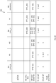
- Fig. 8A is a table 800 that illustrates the status of the ring network 100 at time T0, including: the actions performed by nodes N0-N5, the output messages provided on the message bus 102 by nodes and the contents of the message snoopers of nodes the values of the timestamp counters of nodes the values of the color bits of nodes and the location of the pulse message that continuously travels around the ring network 100.
- the CPU_0 of root node N0 transmits a message M*0_5(0) on the message bus 102 (e.g., as MSG_01).
- M* specifies a point-to-point ordered message
- X specifies the source node ID (i.e., the contents of the node ID register 250 of the node N0 that originates the message)
- Y corresponds with the destination node ID (i.e., the contents of the node ID register of the node N5 to receive the point-to-point ordered message)
- Z corresponds with the timestamp value of the originating node N0 (at the time the message is initially sent).
- message M*0_5(0) specifies a point-to-point ordered message transmitted from node N0 to node N5, initiated when the timestamp counter of node N0 has a value of 0.
- message M*0_5(0) includes additional information (not shown) that indicates that the transaction is an access to a cache line 'A' in the system memory of node N5.
- the CPU_0 of node N0 increments its timestamp counter 255 from a value of 0 to a value of 1.
- the message snooper 230 of node N0 stores the message M*0_5(0).
- the node N2 transmits an ordered point-to-point message M*2_4(0) on the message bus 102 (e.g., as MSG_23).
- message M*2_4(0) specifies a point-to-point ordered message transmitted from node N2 to node N4, initiated when the timestamp counter of node N2 has a value of 0.
- the node N2 increments its timestamp counter from a value of 0 to a value of 1.
- the message snooper of node N2 stores the message M*2_4(0).
- nodes N1 and N3-N5 do not initiate any actions (or provide any messages on the message bus 102) and the message snoopers of nodes N1 and N3-N5 are empty. Because none of these nodes N1 and N3-N5 has received or transmitted a point-to-point ordered message, the timestamp counters of these nodes remain unchanged.
- the pulse message reaches node N4 at time T0, thereby causing the color bit of node N4 to transition from a '0' value to a '1' value.
- the color bit values and the pulse location are arbitrarily selected for the present example.
- Fig. 8B is a table 801 that illustrates the status of the ring network 100 during the next cycle T1.
- none of the nodes N0-N5 transmit any new messages.
- the message M*0_5(0) is received by node N1, and this node N1 stores the message M*0_5(0) in its message snooper. Because node N1 has received a point-to-point ordered message, node N1 increments its timestamp counter from 0 to 1.
- the node logic 310 within node N1 then transmits the point-to-point ordered message M*0_5(0) to node N2.
- the point-to-point ordered message M*2_4(0) is received by node N3, and this node N3 stores the message M*2_4(0) in its message snooper. Because node N3 has received a point-to-point ordered message, node N3 increments its timestamp counter from 0 to 1. The node logic within node N3 then transmits the point-to-point ordered message M*2_4(0) to node N4.
- the pulse message reaches node N5 during cycle T1, thereby causing the color bit of node N5 to toggle from a '0' value to a '1' value.
- Fig. 8C is a table 802 that illustrates the status of the ring network 100 during the next cycle T2.
- the CPU_1 of node N3 transmits a message M*3_5(1) on the message bus 102 (e.g., as MSG_34) and stores this message M*3_5(1) in its message snooper.
- message M*3_5(1) specifies a point-to-point ordered message from node N3 to node N5. Note that the timestamp value of node N3 is '1' at the time the message M*3_5(1) is generated.
- message M*3_5(1) includes additional information (not shown) that indicates that the transaction is an access to a cache line 'A' in the system memory of node N5. Because node N3 has transmitted an ordered message M*3_5(1), the timestamp counter of node N3 is incremented, from 1 to 2. Note that nodes N0-N2 and N4-N5 do not initiate any new actions during cycle T2.
- the point-to-point ordered message M*0_5(0) is received by node N2, and this node N2 stores the message M*0_5(0) in its message snooper. Because node N2 has received an ordered message, node N2 increments its timestamp counter from 1 to 2. The node logic within node N2 then transmits the point-to-point ordered message M*0_5(0) to node N3.
- the point-to-point ordered message M*2_4(0) is received by node N4, and this node N4 stores the message M*2_4(0) in its message snooper. Because node N4 has received an ordered message, node N4 increments its timestamp counter from 0 to 1. The node logic within node N4 then transmits the point-to-point ordered message M*2_4(0) to node N5.
- the pulse message reaches node N0 during cycle T2, thereby causing the color bit of node N0 to toggle from a '1' value to a '0' value.
- Fig. 8D is a table 803 that illustrates the status of the ring network 100 during the next cycle T3.
- nodes N0-N5 transmit any new messages.
- the point-to-point ordered message M*0_5(0) is received by node N3, and this node N3 stores the message M*0_5(0) in its message snooper. Because node N3 has received an ordered message, node N3 increments its timestamp counter from 2 to 3. Node logic within node N3 then transmits the point-to-point ordered message M*0_5(0) to node N4.
- the point-to-point ordered message M*2_4(0) is received by node N5, and this node N5 stores the message M*2_4(0) in its message snooper. Because node N5 has received an ordered message, node N5 increments its timestamp counter from 0 to 1. The node logic within node N5 then transmits the point-to-point ordered message M*2_4(0) to node N0.
- the point-to-point ordered message M*3_5(1) is received by node N4, and this node N4 stores the message M*3_5(1) in its message snooper. Because node N4 has received an ordered message, node N4 increments its timestamp counter from 1 to 2. Node logic within node N4 then transmits the point-to-point ordered message M*3_5(1) to node N5.
- the pulse message reaches node N1 during cycle T3, thereby causing the color bit of node N1 to toggle from a '1' value to a '0' value.
- Fig. 8E is a table 804 that illustrates the status of the ring network 100 during the next cycle T4.
- nodes N0-N5 transmit any new messages.
- the point-to-point ordered message M*0_5(0) is received by node N4, and this node N4 stores the message M*0_5(0) in its message snooper. Because node N4 has received an ordered message, node N4 increments its timestamp counter from 2 to 3.
- the node logic within node N4 then transmits the point-to-point ordered message M*0_5(0) to node N5.
- the point-to-point ordered message M*2_4(0) is received by node N0, and this node N0 stores the message M*2_4(0) in its message snooper. Because node N0 has received an ordered message, node N0 increments its timestamp counter from 1 to 2. The node logic within node N0 then transmits the point-to-point ordered message M*2_4(0) to node N1.
- node N5 To ensure that node N5 resolves point-to-point ordered messages in the proper order, node N5 must wait to resolve the received point-to-point ordered message M*3_5(1) until the value of the color bit is toggled (e.g., the color bit transitions to a value of 0 within node N5). The node logic of node N5 then transmits the point-to-point ordered message M*3_5(1) to node N0.
- the pulse message reaches node N2 during cycle T4, thereby causing the color bit of node N2 to toggle from a '1' value to a '0' value.
- Fig. 8F is a table 805 that illustrates the status of the ring network 100 during the next cycle T5.
- node N5 receives the point-to-point ordered message M*0_5(0) from node N5
- this node N5 stores the message M*0_5(0) in its message snooper.
- node N5 To ensure that node N5 resolves ordered messages in the proper order, node N5 must wait to resolve the received point-to-point ordered message M*0_5(0) until the value of the color bit is toggled (e.g., the color bit transitions to a value of 0 within node N5). The node logic of node N5 then transmits the point-to-point ordered message M*0_5(0) to node N0.
- the point-to-point ordered message M*2_4(0) is received by node N1, and this node N1 stores the message M*2_4(0) in its message snooper. Because node N1 has received an ordered message, node N1 increments its timestamp counter from 1 to 2. The node logic of node N1 then transmits the message M*2_4(0) to node N2.
- the point-to-point ordered message M*3_5(1) is received by node N0, and this node N0 stores the message M*3_5(1) in its message snooper. Because node N0 has received an ordered message, node N0 increments its timestamp counter from 2 to 3. The node logic of node N0 then transmits the point-to-point ordered message M*3_5(1) to node N1.
- the pulse message reaches node N3 during cycle T5, thereby causing the color bit of node N3 to toggle from a '1' value to a '0' value.
- Fig. 8G is a table 806 that illustrates the status of the ring network 100 during the next cycle T6.
- none of the nodes N0-N5 transmit any new messages.
- the point-to-point ordered message M*0_5(0) loops back to the originating node N0.
- node N0 stops the propagation of this message M*0_5(0) on ring network 200. Note that node N0 does not increment its timestamp counter in response to receiving the ordered message that it originally transmitted.
- node N0 Upon receiving the message M*0_5(0), node N0 accesses its message snooper, and compares the stored ordered messages to determine that its point-to-point ordered message M*0_5(0) has priority over the other point-to-point ordered message M*3_5(1) that addressed the same node N5 (because the message M*0_5(0) has a lower timestamp than the other ordered message M*3_5(1)). As a result, node N0 is informed that its point-to-point ordered message M*0_5(0) will be awarded priority by node N5, and will be processed by node N5.
- the point-to-point ordered message M*2_4(0) loops back to the originating node N2.
- node N2 stops the propagation of this message M*2_4(0) on ring network 200.
- Node N2 does not increment its timestamp counter in response to receiving the ordered message that it originally transmitted.
- node N2 accesses its message snooper, and compares the stored ordered messages to determine that its message M*2_4(0) has priority over the other ordered messages stored in its message snooper (because none of these other messages addresses node N4).
- node N2 is informed that its message M*2_4(0) will be awarded priority by node N4, and will be processed by node N4.
- the point-to-point ordered message M*3_5(1) is received by node N1, and this node N1 stores the message M*3_5(1) in its message snooper. Because node N1 has received an ordered message, node N1 increments its timestamp counter from 2 to 3. The node logic of node N1 then transmits the point-to-point ordered message M*3_5(1) to node N2.
- the pulse message reaches node N4 during cycle T6, thereby causing the color bit of node N4 to toggle from a '1' value to a '0' value.
- node N4 resolves the priority of the ordered messages stored in its message snooper in response to the toggling of its color bit. As described above, node N4 awards priority to the only ordered message M*2_4(0) in its message buffer that addressed node N4.
- Fig. 8H is a table 807 that illustrates the status of the ring network 100 during the next cycle T7.
- none of the nodes N0-N5 transmit any new messages.
- the pulse message reaches node N5 during cycle T7, thereby causing the color bit of node N5 to toggle from a '1' value to a '0' value.
- node N5 performs arbitration of the ordered messages stored in its message snooper while the color bit had the previous value of '1'.
- node N5 determines that point-to-point ordered message M*0_5(0) has priority over other point-to-point ordered message M*3_5(1), because the message M*0_5(0) has a lower timestamp value than the other message M*3_5(1).
- node N5 will access the data requested by message M*0_5(0) in cache line 'A' of the system memory. Note that node N5 will generate a separate message (not shown) transmitting this requested data to node N0. Further note that node N5 ignores the point-to-point ordered message M*2_4(0) stored in its message snooper, because this message does not address node N5.
- the point-to-point ordered message M*3_5(1) is received by node N2, and this node N2 stores the message M*3_5(1) in its message snooper. Because node N2 has received an ordered message, node N2 increments its timestamp counter from 2 to 3. The node logic of node N2 then transmits the point-to-point ordered message M*3_5(1) to node N3.
- Fig. 8I is a table 808 that illustrates the status of the ring network 100 during the next cycle T8.
- none of the nodes N0-N5 transmit any new messages.
- the point-to-point ordered message M*3_5(1) loops back to the originating node N3.
- node N3 stops the propagation of this message M*3_5(1) on ring network 200.
- Node N3 does not increment its timestamp counter in response to receiving the point-to-point ordered message that it originally transmitted.
- node N3 Upon receiving the message M*3_5(1), node N3 accesses its message snooper, and compares the stored ordered messages to determine that the point-to-point ordered message M*0_5(0) transmitted by node N0 has priority over its own point-to-point ordered message M*3_5(1) (because message M*0_5(0) has a lower timestamp value than message M*3_5(1)). As a result, node N3 is informed that its message M*3_5(1) will not be awarded priority by node N5, and will be not be processed by node N5. In response, node N3 may determine that the message M*3_5(1) should be retransmitted.
- point-to-point ordered messages can be processed by ring network 100 without requiring a complex centralized control circuit.
- the required control logic is advantageously distributed among the nodes, such that no centralized controller is necessary.
- it is unnecessary to design/fabricate an extensive low skew clock tree across a large die area, thereby advantageously simplifying the physical implementation of the network.
- the ring network 100 can be operated at a high frequency with minimal latency.
- bandwidth allocation policies and flow control logic are necessarily included within the client logic of each node.
- bandwidth allocation policies and flow control logic can be used by the bandwidth allocation and flow control circuit within each node.
- the bandwidth allocation and flow control logic of each node will operate in the client logic clock domain, and therefore can operate at a different frequency than the reference clock signal CK_REF of the ring network clock domain.
Landscapes
- Engineering & Computer Science (AREA)
- Computer Networks & Wireless Communication (AREA)
- Signal Processing (AREA)
- Theoretical Computer Science (AREA)
- Physics & Mathematics (AREA)
- Computer Hardware Design (AREA)
- General Engineering & Computer Science (AREA)
- General Physics & Mathematics (AREA)
- Evolutionary Computation (AREA)
- Geometry (AREA)
- Multi Processors (AREA)
- Small-Scale Networks (AREA)
Applications Claiming Priority (3)
| Application Number | Priority Date | Filing Date | Title |
|---|---|---|---|
| US201662425792P | 2016-11-23 | 2016-11-23 | |
| US15/816,235 US10411910B2 (en) | 2016-11-23 | 2017-11-17 | Distributed control synchronized ring network architecture |
| PCT/US2017/062627 WO2018098084A2 (en) | 2016-11-23 | 2017-11-20 | Distributed control synchronized ring network architecture |
Publications (3)
| Publication Number | Publication Date |
|---|---|
| EP3545653A2 EP3545653A2 (en) | 2019-10-02 |
| EP3545653A4 EP3545653A4 (en) | 2021-01-27 |
| EP3545653B1 true EP3545653B1 (en) | 2022-01-05 |
Family
ID=62144074
Family Applications (1)
| Application Number | Title | Priority Date | Filing Date |
|---|---|---|---|
| EP17874888.5A Active EP3545653B1 (en) | 2016-11-23 | 2017-11-20 | Distributed control synchronized ring network architecture |
Country Status (9)
| Country | Link |
|---|---|
| US (1) | US10411910B2 (zh) |
| EP (1) | EP3545653B1 (zh) |
| JP (1) | JP7014812B2 (zh) |
| KR (1) | KR102214874B1 (zh) |
| CN (1) | CN110546922B (zh) |
| CA (1) | CA3044672C (zh) |
| ES (1) | ES2903557T3 (zh) |
| TW (1) | TWI730197B (zh) |
| WO (1) | WO2018098084A2 (zh) |
Families Citing this family (6)
| Publication number | Priority date | Publication date | Assignee | Title |
|---|---|---|---|---|
| DE102017011458A1 (de) * | 2017-12-12 | 2019-06-13 | WAGO Verwaltungsgesellschaft mit beschränkter Haftung | Teilnehmer eines Bussystems, Verfahren zum Betrieb und ein Bussystem |
| US11829196B2 (en) * | 2019-10-22 | 2023-11-28 | Advanced Micro Devices, Inc. | Ring transport employing clock wake suppression |
| JP7231909B2 (ja) * | 2019-11-12 | 2023-03-02 | 株式会社アーリーワークス | 情報処理装置及びプログラム |
| CN111884901B (zh) * | 2020-07-01 | 2021-10-22 | 浙江杰芯科技有限公司 | 一种基于环形网络的时钟同步路径查询方法及系统 |
| WO2022087985A1 (zh) * | 2020-10-29 | 2022-05-05 | 华为技术有限公司 | 控制系统、时钟同步方法、控制器、节点设备及车辆 |
| WO2023211320A1 (en) * | 2022-04-25 | 2023-11-02 | Saab Ab | Method for generating a non-jittering trigger signal in a node of a serial data ring-bus |
Family Cites Families (37)
| Publication number | Priority date | Publication date | Assignee | Title |
|---|---|---|---|---|
| JPS58127246A (ja) * | 1982-01-26 | 1983-07-29 | Nec Corp | リングバスインタフエイス回路 |
| US4716575A (en) * | 1982-03-25 | 1987-12-29 | Apollo Computer, Inc. | Adaptively synchronized ring network for data communication |
| US5539727A (en) * | 1992-04-14 | 1996-07-23 | Kramarczyk; Marian | Method and apparatus for configuring and maintaining token ring networks |
| JPH06332852A (ja) * | 1993-05-20 | 1994-12-02 | Hitachi Ltd | データ転送システム |
| US5815016A (en) | 1994-09-02 | 1998-09-29 | Xilinx, Inc. | Phase-locked delay loop for clock correction |
| US6574219B1 (en) * | 1998-08-06 | 2003-06-03 | Intel Corp | Passive message ordering on a decentralized ring |
| US6523155B1 (en) * | 1998-11-17 | 2003-02-18 | Jeffrey Joseph Ruedinger | Method for partitioning a netlist into multiple clock domains |
| JP2002141922A (ja) * | 2000-11-01 | 2002-05-17 | Ricoh Co Ltd | ループ型バスシステム |
| US7012927B2 (en) | 2001-02-06 | 2006-03-14 | Honeywell International Inc. | High level message priority assignment by a plurality of message-sending nodes sharing a signal bus |
| US6570813B2 (en) * | 2001-05-25 | 2003-05-27 | Micron Technology, Inc. | Synchronous mirror delay with reduced delay line taps |
| US6990316B2 (en) | 2001-06-26 | 2006-01-24 | Nokia Corporation | Short range RF network configuration |
| US20030172190A1 (en) * | 2001-07-02 | 2003-09-11 | Globespanvirata Incorporated | Communications system using rings architecture |
| US6961861B2 (en) * | 2002-02-27 | 2005-11-01 | Sun Microsystems, Inc. | Globally clocked interfaces having reduced data path length |
| US7280550B1 (en) * | 2002-12-18 | 2007-10-09 | Cirrus Logic, Inc. | Bandwidth optimization of ring topology through propagation delay compensation |
| US7292585B1 (en) | 2002-12-20 | 2007-11-06 | Symantec Operating Corporation | System and method for storing and utilizing routing information in a computer network |
| US7769956B2 (en) * | 2005-09-07 | 2010-08-03 | Intel Corporation | Pre-coherence channel |
| US7885296B2 (en) | 2006-07-27 | 2011-02-08 | Cisco Technology, Inc. | Maintaining consistency among multiple timestamp counters distributed among multiple devices |
| US7809871B2 (en) | 2006-12-07 | 2010-10-05 | Integrated Device Technology Inc. | Common access ring system |
| JP5327832B2 (ja) * | 2007-05-16 | 2013-10-30 | 独立行政法人情報通信研究機構 | ノード識別子と位置指示子とを用いたパケットの通信方法 |
| ATE536681T1 (de) * | 2007-10-04 | 2011-12-15 | Harman Becker Automotive Sys | Datennetzwerk mit zeitsynchronisationsmechanismus |
| US7864747B2 (en) | 2008-03-28 | 2011-01-04 | Embarq Holdings Company, Llc | System and method for communicating timing to a remote node |
| US8261218B1 (en) * | 2008-08-01 | 2012-09-04 | Altera Corporation | Systems and methods for determining beneficial clock-path connection delays |
| KR101299443B1 (ko) * | 2009-05-15 | 2013-08-22 | 한국전자통신연구원 | 보호 절체 방법 |
| CN102064927B (zh) * | 2010-09-21 | 2013-11-13 | 四川和芯微电子股份有限公司 | 时序纠错系统及方法 |
| US9247157B2 (en) * | 2011-05-13 | 2016-01-26 | Lattice Semiconductor Corporation | Audio and video data multiplexing for multimedia stream switch |
| US8995473B2 (en) | 2012-04-20 | 2015-03-31 | Telefonaktiebolaget L M Ericsson (Publ) | Ring based precise time data network clock phase adjustments |
| US9294301B2 (en) * | 2012-09-20 | 2016-03-22 | Arm Limited | Selecting between contending data packets to limit latency differences between sources |
| US9053257B2 (en) * | 2012-11-05 | 2015-06-09 | Advanced Micro Devices, Inc. | Voltage-aware signal path synchronization |
| WO2014145066A2 (en) * | 2013-03-15 | 2014-09-18 | Qualcomm Incorporated | Low power architectures |
| US9652804B2 (en) * | 2013-12-19 | 2017-05-16 | Chicago Mercantile Exchange Inc. | Deterministic and efficient message packet management |
| US9355054B2 (en) * | 2014-01-07 | 2016-05-31 | Omnivision Technologies, Inc. | Digital calibration-based skew cancellation for long-reach MIPI D-PHY serial links |
| CN104796212B (zh) * | 2014-01-22 | 2019-07-05 | 中兴通讯股份有限公司 | 一种光突发传送网、节点和传输方法 |
| US9209961B1 (en) * | 2014-09-29 | 2015-12-08 | Apple Inc. | Method and apparatus for delay compensation in data transmission |
| EP3015971B1 (en) * | 2014-10-28 | 2019-07-31 | Napatech A/S | A system and a method of deriving information |
| US9755955B2 (en) * | 2015-02-18 | 2017-09-05 | Accedian Networks Inc. | Single queue link aggregation |
| TW201735581A (zh) * | 2016-03-16 | 2017-10-01 | 瑞昱半導體股份有限公司 | 網路通訊裝置與電子裝置 |
| US10496581B2 (en) * | 2016-03-30 | 2019-12-03 | Intel Corporation | Un-sampled decision feedback equalizer including configurable loop delay |
-
2017
- 2017-11-17 US US15/816,235 patent/US10411910B2/en active Active
- 2017-11-20 EP EP17874888.5A patent/EP3545653B1/en active Active
- 2017-11-20 ES ES17874888T patent/ES2903557T3/es active Active
- 2017-11-20 TW TW106140091A patent/TWI730197B/zh active
- 2017-11-20 CN CN201780083717.9A patent/CN110546922B/zh active Active
- 2017-11-20 CA CA3044672A patent/CA3044672C/en active Active
- 2017-11-20 WO PCT/US2017/062627 patent/WO2018098084A2/en unknown
- 2017-11-20 KR KR1020197017774A patent/KR102214874B1/ko active IP Right Grant
- 2017-11-20 JP JP2019547588A patent/JP7014812B2/ja active Active
Also Published As
| Publication number | Publication date |
|---|---|
| JP7014812B2 (ja) | 2022-02-01 |
| EP3545653A2 (en) | 2019-10-02 |
| US20180145849A1 (en) | 2018-05-24 |
| KR20190085992A (ko) | 2019-07-19 |
| ES2903557T3 (es) | 2022-04-04 |
| TW201832470A (zh) | 2018-09-01 |
| CN110546922B (zh) | 2022-05-10 |
| WO2018098084A2 (en) | 2018-05-31 |
| CN110546922A (zh) | 2019-12-06 |
| WO2018098084A3 (en) | 2019-12-05 |
| US10411910B2 (en) | 2019-09-10 |
| EP3545653A4 (en) | 2021-01-27 |
| CA3044672C (en) | 2023-08-29 |
| KR102214874B1 (ko) | 2021-02-09 |
| TWI730197B (zh) | 2021-06-11 |
| CA3044672A1 (en) | 2018-05-31 |
| JP2020508625A (ja) | 2020-03-19 |
Similar Documents
| Publication | Publication Date | Title |
|---|---|---|
| EP3545653B1 (en) | Distributed control synchronized ring network architecture | |
| US11196587B2 (en) | Permutated ring network | |
| US10355851B2 (en) | Methods and systems for synchronization between multiple clock domains | |
| US10027433B2 (en) | Multiple clock domains in NoC | |
| US7925803B2 (en) | Method and systems for mesochronous communications in multiple clock domains and corresponding computer program product | |
| US20080005402A1 (en) | Gals-based network-on-chip and data transfer method thereof | |
| CN111447031B (zh) | 一种具有时钟同步功能的片上网络路由器结构 | |
| JP7565467B2 (ja) | 非同期asic | |
| Weber et al. | Exploring asynchronous end-to-end communication through a synchronous NoC | |
| JP7337021B2 (ja) | 産業用ネットワークに接続されるスレーブ装置を制御するマスタ装置及び当該マスタ装置に備えられる通信モジュール | |
| US7861018B2 (en) | System for transmitting data between transmitter and receiver modules on a channel provided with a flow control link |
Legal Events
| Date | Code | Title | Description |
|---|---|---|---|
| STAA | Information on the status of an ep patent application or granted ep patent |
Free format text: STATUS: THE INTERNATIONAL PUBLICATION HAS BEEN MADE |
|
| PUAI | Public reference made under article 153(3) epc to a published international application that has entered the european phase |
Free format text: ORIGINAL CODE: 0009012 |
|
| STAA | Information on the status of an ep patent application or granted ep patent |
Free format text: STATUS: REQUEST FOR EXAMINATION WAS MADE |
|
| 17P | Request for examination filed |
Effective date: 20190613 |
|
| AK | Designated contracting states |
Kind code of ref document: A2 Designated state(s): AL AT BE BG CH CY CZ DE DK EE ES FI FR GB GR HR HU IE IS IT LI LT LU LV MC MK MT NL NO PL PT RO RS SE SI SK SM TR |
|
| AX | Request for extension of the european patent |
Extension state: BA ME |
|
| R17D | Deferred search report published (corrected) |
Effective date: 20191205 |
|
| DAV | Request for validation of the european patent (deleted) | ||
| DAX | Request for extension of the european patent (deleted) | ||
| A4 | Supplementary search report drawn up and despatched |
Effective date: 20210113 |
|
| RIC1 | Information provided on ipc code assigned before grant |
Ipc: H04L 7/04 20060101ALI20201222BHEP Ipc: H04L 12/42 20060101AFI20201222BHEP Ipc: G06F 30/396 20200101ALI20201222BHEP Ipc: G06F 1/10 20060101ALI20201222BHEP Ipc: H04L 7/00 20060101ALI20201222BHEP Ipc: H04L 12/437 20060101ALI20201222BHEP Ipc: H04J 3/06 20060101ALI20201222BHEP |
|
| GRAP | Despatch of communication of intention to grant a patent |
Free format text: ORIGINAL CODE: EPIDOSNIGR1 |
|
| STAA | Information on the status of an ep patent application or granted ep patent |
Free format text: STATUS: GRANT OF PATENT IS INTENDED |
|
| RIC1 | Information provided on ipc code assigned before grant |
Ipc: H04L 7/00 20060101ALI20210824BHEP Ipc: H04J 3/06 20060101ALI20210824BHEP Ipc: G06F 30/396 20200101ALI20210824BHEP Ipc: G06F 1/10 20060101ALI20210824BHEP Ipc: H04L 12/437 20060101ALI20210824BHEP Ipc: H04L 7/04 20060101ALI20210824BHEP Ipc: H04L 12/42 20060101AFI20210824BHEP |
|
| INTG | Intention to grant announced |
Effective date: 20210909 |
|
| GRAS | Grant fee paid |
Free format text: ORIGINAL CODE: EPIDOSNIGR3 |
|
| GRAA | (expected) grant |
Free format text: ORIGINAL CODE: 0009210 |
|
| STAA | Information on the status of an ep patent application or granted ep patent |
Free format text: STATUS: THE PATENT HAS BEEN GRANTED |
|
| AK | Designated contracting states |
Kind code of ref document: B1 Designated state(s): AL AT BE BG CH CY CZ DE DK EE ES FI FR GB GR HR HU IE IS IT LI LT LU LV MC MK MT NL NO PL PT RO RS SE SI SK SM TR |
|
| REG | Reference to a national code |
Ref country code: GB Ref legal event code: FG4D |
|
| REG | Reference to a national code |
Ref country code: CH Ref legal event code: EP |
|
| REG | Reference to a national code |
Ref country code: AT Ref legal event code: REF Ref document number: 1461563 Country of ref document: AT Kind code of ref document: T Effective date: 20220115 |
|
| REG | Reference to a national code |
Ref country code: DE Ref legal event code: R096 Ref document number: 602017052079 Country of ref document: DE |
|
| REG | Reference to a national code |
Ref country code: IE Ref legal event code: FG4D |
|
| REG | Reference to a national code |
Ref country code: ES Ref legal event code: FG2A Ref document number: 2903557 Country of ref document: ES Kind code of ref document: T3 Effective date: 20220404 |
|
| REG | Reference to a national code |
Ref country code: LT Ref legal event code: MG9D |
|
| REG | Reference to a national code |
Ref country code: NL Ref legal event code: MP Effective date: 20220105 |
|
| REG | Reference to a national code |
Ref country code: AT Ref legal event code: MK05 Ref document number: 1461563 Country of ref document: AT Kind code of ref document: T Effective date: 20220105 |
|
| PG25 | Lapsed in a contracting state [announced via postgrant information from national office to epo] |
Ref country code: NL Free format text: LAPSE BECAUSE OF FAILURE TO SUBMIT A TRANSLATION OF THE DESCRIPTION OR TO PAY THE FEE WITHIN THE PRESCRIBED TIME-LIMIT Effective date: 20220105 |
|
| RAP4 | Party data changed (patent owner data changed or rights of a patent transferred) |
Owner name: DEGIRUM CORPORATION |
|
| PG25 | Lapsed in a contracting state [announced via postgrant information from national office to epo] |
Ref country code: SE Free format text: LAPSE BECAUSE OF FAILURE TO SUBMIT A TRANSLATION OF THE DESCRIPTION OR TO PAY THE FEE WITHIN THE PRESCRIBED TIME-LIMIT Effective date: 20220105 Ref country code: RS Free format text: LAPSE BECAUSE OF FAILURE TO SUBMIT A TRANSLATION OF THE DESCRIPTION OR TO PAY THE FEE WITHIN THE PRESCRIBED TIME-LIMIT Effective date: 20220105 Ref country code: PT Free format text: LAPSE BECAUSE OF FAILURE TO SUBMIT A TRANSLATION OF THE DESCRIPTION OR TO PAY THE FEE WITHIN THE PRESCRIBED TIME-LIMIT Effective date: 20220505 Ref country code: NO Free format text: LAPSE BECAUSE OF FAILURE TO SUBMIT A TRANSLATION OF THE DESCRIPTION OR TO PAY THE FEE WITHIN THE PRESCRIBED TIME-LIMIT Effective date: 20220405 Ref country code: LT Free format text: LAPSE BECAUSE OF FAILURE TO SUBMIT A TRANSLATION OF THE DESCRIPTION OR TO PAY THE FEE WITHIN THE PRESCRIBED TIME-LIMIT Effective date: 20220105 Ref country code: HR Free format text: LAPSE BECAUSE OF FAILURE TO SUBMIT A TRANSLATION OF THE DESCRIPTION OR TO PAY THE FEE WITHIN THE PRESCRIBED TIME-LIMIT Effective date: 20220105 Ref country code: BG Free format text: LAPSE BECAUSE OF FAILURE TO SUBMIT A TRANSLATION OF THE DESCRIPTION OR TO PAY THE FEE WITHIN THE PRESCRIBED TIME-LIMIT Effective date: 20220405 |
|
| PG25 | Lapsed in a contracting state [announced via postgrant information from national office to epo] |
Ref country code: PL Free format text: LAPSE BECAUSE OF FAILURE TO SUBMIT A TRANSLATION OF THE DESCRIPTION OR TO PAY THE FEE WITHIN THE PRESCRIBED TIME-LIMIT Effective date: 20220105 Ref country code: LV Free format text: LAPSE BECAUSE OF FAILURE TO SUBMIT A TRANSLATION OF THE DESCRIPTION OR TO PAY THE FEE WITHIN THE PRESCRIBED TIME-LIMIT Effective date: 20220105 Ref country code: GR Free format text: LAPSE BECAUSE OF FAILURE TO SUBMIT A TRANSLATION OF THE DESCRIPTION OR TO PAY THE FEE WITHIN THE PRESCRIBED TIME-LIMIT Effective date: 20220406 Ref country code: FI Free format text: LAPSE BECAUSE OF FAILURE TO SUBMIT A TRANSLATION OF THE DESCRIPTION OR TO PAY THE FEE WITHIN THE PRESCRIBED TIME-LIMIT Effective date: 20220105 Ref country code: AT Free format text: LAPSE BECAUSE OF FAILURE TO SUBMIT A TRANSLATION OF THE DESCRIPTION OR TO PAY THE FEE WITHIN THE PRESCRIBED TIME-LIMIT Effective date: 20220105 |
|
| PG25 | Lapsed in a contracting state [announced via postgrant information from national office to epo] |
Ref country code: IS Free format text: LAPSE BECAUSE OF FAILURE TO SUBMIT A TRANSLATION OF THE DESCRIPTION OR TO PAY THE FEE WITHIN THE PRESCRIBED TIME-LIMIT Effective date: 20220505 |
|
| REG | Reference to a national code |
Ref country code: DE Ref legal event code: R097 Ref document number: 602017052079 Country of ref document: DE |
|
| PG25 | Lapsed in a contracting state [announced via postgrant information from national office to epo] |
Ref country code: SM Free format text: LAPSE BECAUSE OF FAILURE TO SUBMIT A TRANSLATION OF THE DESCRIPTION OR TO PAY THE FEE WITHIN THE PRESCRIBED TIME-LIMIT Effective date: 20220105 Ref country code: SK Free format text: LAPSE BECAUSE OF FAILURE TO SUBMIT A TRANSLATION OF THE DESCRIPTION OR TO PAY THE FEE WITHIN THE PRESCRIBED TIME-LIMIT Effective date: 20220105 Ref country code: RO Free format text: LAPSE BECAUSE OF FAILURE TO SUBMIT A TRANSLATION OF THE DESCRIPTION OR TO PAY THE FEE WITHIN THE PRESCRIBED TIME-LIMIT Effective date: 20220105 Ref country code: EE Free format text: LAPSE BECAUSE OF FAILURE TO SUBMIT A TRANSLATION OF THE DESCRIPTION OR TO PAY THE FEE WITHIN THE PRESCRIBED TIME-LIMIT Effective date: 20220105 Ref country code: DK Free format text: LAPSE BECAUSE OF FAILURE TO SUBMIT A TRANSLATION OF THE DESCRIPTION OR TO PAY THE FEE WITHIN THE PRESCRIBED TIME-LIMIT Effective date: 20220105 Ref country code: CZ Free format text: LAPSE BECAUSE OF FAILURE TO SUBMIT A TRANSLATION OF THE DESCRIPTION OR TO PAY THE FEE WITHIN THE PRESCRIBED TIME-LIMIT Effective date: 20220105 |
|
| PLBE | No opposition filed within time limit |
Free format text: ORIGINAL CODE: 0009261 |
|
| STAA | Information on the status of an ep patent application or granted ep patent |
Free format text: STATUS: NO OPPOSITION FILED WITHIN TIME LIMIT |
|
| PG25 | Lapsed in a contracting state [announced via postgrant information from national office to epo] |
Ref country code: AL Free format text: LAPSE BECAUSE OF FAILURE TO SUBMIT A TRANSLATION OF THE DESCRIPTION OR TO PAY THE FEE WITHIN THE PRESCRIBED TIME-LIMIT Effective date: 20220105 |
|
| 26N | No opposition filed |
Effective date: 20221006 |
|
| PG25 | Lapsed in a contracting state [announced via postgrant information from national office to epo] |
Ref country code: SI Free format text: LAPSE BECAUSE OF FAILURE TO SUBMIT A TRANSLATION OF THE DESCRIPTION OR TO PAY THE FEE WITHIN THE PRESCRIBED TIME-LIMIT Effective date: 20220105 |
|
| P01 | Opt-out of the competence of the unified patent court (upc) registered |
Effective date: 20230414 |
|
| PG25 | Lapsed in a contracting state [announced via postgrant information from national office to epo] |
Ref country code: MC Free format text: LAPSE BECAUSE OF FAILURE TO SUBMIT A TRANSLATION OF THE DESCRIPTION OR TO PAY THE FEE WITHIN THE PRESCRIBED TIME-LIMIT Effective date: 20220105 |
|
| REG | Reference to a national code |
Ref country code: CH Ref legal event code: PL |
|
| REG | Reference to a national code |
Ref country code: BE Ref legal event code: MM Effective date: 20221130 |
|
| PG25 | Lapsed in a contracting state [announced via postgrant information from national office to epo] |
Ref country code: LI Free format text: LAPSE BECAUSE OF NON-PAYMENT OF DUE FEES Effective date: 20221130 Ref country code: CH Free format text: LAPSE BECAUSE OF NON-PAYMENT OF DUE FEES Effective date: 20221130 |
|
| PG25 | Lapsed in a contracting state [announced via postgrant information from national office to epo] |
Ref country code: LU Free format text: LAPSE BECAUSE OF NON-PAYMENT OF DUE FEES Effective date: 20221120 |
|
| PG25 | Lapsed in a contracting state [announced via postgrant information from national office to epo] |
Ref country code: IE Free format text: LAPSE BECAUSE OF NON-PAYMENT OF DUE FEES Effective date: 20221120 |
|
| PG25 | Lapsed in a contracting state [announced via postgrant information from national office to epo] |
Ref country code: BE Free format text: LAPSE BECAUSE OF NON-PAYMENT OF DUE FEES Effective date: 20221130 |
|
| PGFP | Annual fee paid to national office [announced via postgrant information from national office to epo] |
Ref country code: GB Payment date: 20231121 Year of fee payment: 7 |
|
| PGFP | Annual fee paid to national office [announced via postgrant information from national office to epo] |
Ref country code: ES Payment date: 20231218 Year of fee payment: 7 |
|
| PGFP | Annual fee paid to national office [announced via postgrant information from national office to epo] |
Ref country code: IT Payment date: 20231124 Year of fee payment: 7 Ref country code: FR Payment date: 20231123 Year of fee payment: 7 Ref country code: DE Payment date: 20231127 Year of fee payment: 7 |
|
| PG25 | Lapsed in a contracting state [announced via postgrant information from national office to epo] |
Ref country code: HU Free format text: LAPSE BECAUSE OF FAILURE TO SUBMIT A TRANSLATION OF THE DESCRIPTION OR TO PAY THE FEE WITHIN THE PRESCRIBED TIME-LIMIT; INVALID AB INITIO Effective date: 20171120 |
|
| PG25 | Lapsed in a contracting state [announced via postgrant information from national office to epo] |
Ref country code: CY Free format text: LAPSE BECAUSE OF FAILURE TO SUBMIT A TRANSLATION OF THE DESCRIPTION OR TO PAY THE FEE WITHIN THE PRESCRIBED TIME-LIMIT Effective date: 20220105 |
|
| PG25 | Lapsed in a contracting state [announced via postgrant information from national office to epo] |
Ref country code: MK Free format text: LAPSE BECAUSE OF FAILURE TO SUBMIT A TRANSLATION OF THE DESCRIPTION OR TO PAY THE FEE WITHIN THE PRESCRIBED TIME-LIMIT Effective date: 20220105 |
|
| PG25 | Lapsed in a contracting state [announced via postgrant information from national office to epo] |
Ref country code: MT Free format text: LAPSE BECAUSE OF FAILURE TO SUBMIT A TRANSLATION OF THE DESCRIPTION OR TO PAY THE FEE WITHIN THE PRESCRIBED TIME-LIMIT Effective date: 20220105 |