EP3545559B1 - Avalanche photodiode sensor - Google Patents
Avalanche photodiode sensor Download PDFInfo
- Publication number
- EP3545559B1 EP3545559B1 EP18772919.9A EP18772919A EP3545559B1 EP 3545559 B1 EP3545559 B1 EP 3545559B1 EP 18772919 A EP18772919 A EP 18772919A EP 3545559 B1 EP3545559 B1 EP 3545559B1
- Authority
- EP
- European Patent Office
- Prior art keywords
- region
- photodiode
- contact
- vehicle
- avalanche photodiode
- Prior art date
- Legal status (The legal status is an assumption and is not a legal conclusion. Google has not performed a legal analysis and makes no representation as to the accuracy of the status listed.)
- Active
Links
Images


Classifications
-
- G—PHYSICS
- G01—MEASURING; TESTING
- G01J—MEASUREMENT OF INTENSITY, VELOCITY, SPECTRAL CONTENT, POLARISATION, PHASE OR PULSE CHARACTERISTICS OF INFRARED, VISIBLE OR ULTRAVIOLET LIGHT; COLORIMETRY; RADIATION PYROMETRY
- G01J1/00—Photometry, e.g. photographic exposure meter
- G01J1/42—Photometry, e.g. photographic exposure meter using electric radiation detectors
- G01J1/44—Electric circuits
-
- H—ELECTRICITY
- H10—SEMICONDUCTOR DEVICES; ELECTRIC SOLID-STATE DEVICES NOT OTHERWISE PROVIDED FOR
- H10F—INORGANIC SEMICONDUCTOR DEVICES SENSITIVE TO INFRARED RADIATION, LIGHT, ELECTROMAGNETIC RADIATION OF SHORTER WAVELENGTH OR CORPUSCULAR RADIATION
- H10F30/00—Individual radiation-sensitive semiconductor devices in which radiation controls the flow of current through the devices, e.g. photodetectors
- H10F30/20—Individual radiation-sensitive semiconductor devices in which radiation controls the flow of current through the devices, e.g. photodetectors the devices having potential barriers, e.g. phototransistors
- H10F30/21—Individual radiation-sensitive semiconductor devices in which radiation controls the flow of current through the devices, e.g. photodetectors the devices having potential barriers, e.g. phototransistors the devices being sensitive to infrared, visible or ultraviolet radiation
- H10F30/22—Individual radiation-sensitive semiconductor devices in which radiation controls the flow of current through the devices, e.g. photodetectors the devices having potential barriers, e.g. phototransistors the devices being sensitive to infrared, visible or ultraviolet radiation the devices having only one potential barrier, e.g. photodiodes
- H10F30/225—Individual radiation-sensitive semiconductor devices in which radiation controls the flow of current through the devices, e.g. photodetectors the devices having potential barriers, e.g. phototransistors the devices being sensitive to infrared, visible or ultraviolet radiation the devices having only one potential barrier, e.g. photodiodes the potential barrier working in avalanche mode, e.g. avalanche photodiodes
-
- H—ELECTRICITY
- H10—SEMICONDUCTOR DEVICES; ELECTRIC SOLID-STATE DEVICES NOT OTHERWISE PROVIDED FOR
- H10F—INORGANIC SEMICONDUCTOR DEVICES SENSITIVE TO INFRARED RADIATION, LIGHT, ELECTROMAGNETIC RADIATION OF SHORTER WAVELENGTH OR CORPUSCULAR RADIATION
- H10F77/00—Constructional details of devices covered by this subclass
- H10F77/10—Semiconductor bodies
- H10F77/14—Shape of semiconductor bodies; Shapes, relative sizes or dispositions of semiconductor regions within semiconductor bodies
-
- H—ELECTRICITY
- H10—SEMICONDUCTOR DEVICES; ELECTRIC SOLID-STATE DEVICES NOT OTHERWISE PROVIDED FOR
- H10F—INORGANIC SEMICONDUCTOR DEVICES SENSITIVE TO INFRARED RADIATION, LIGHT, ELECTROMAGNETIC RADIATION OF SHORTER WAVELENGTH OR CORPUSCULAR RADIATION
- H10F77/00—Constructional details of devices covered by this subclass
- H10F77/20—Electrodes
-
- H—ELECTRICITY
- H10—SEMICONDUCTOR DEVICES; ELECTRIC SOLID-STATE DEVICES NOT OTHERWISE PROVIDED FOR
- H10F—INORGANIC SEMICONDUCTOR DEVICES SENSITIVE TO INFRARED RADIATION, LIGHT, ELECTROMAGNETIC RADIATION OF SHORTER WAVELENGTH OR CORPUSCULAR RADIATION
- H10F77/00—Constructional details of devices covered by this subclass
- H10F77/93—Interconnections
-
- G—PHYSICS
- G01—MEASURING; TESTING
- G01J—MEASUREMENT OF INTENSITY, VELOCITY, SPECTRAL CONTENT, POLARISATION, PHASE OR PULSE CHARACTERISTICS OF INFRARED, VISIBLE OR ULTRAVIOLET LIGHT; COLORIMETRY; RADIATION PYROMETRY
- G01J1/00—Photometry, e.g. photographic exposure meter
- G01J1/42—Photometry, e.g. photographic exposure meter using electric radiation detectors
- G01J1/44—Electric circuits
- G01J2001/4446—Type of detector
- G01J2001/446—Photodiode
- G01J2001/4466—Avalanche
Definitions
- the pixel capacity represents electrostatic capacity of a pixel in which the SPAD is provided.
- time necessary to take out charges collected in the pixel to perform recharge is lengthened, and thus it is difficult to improve a frame rate.
- the pixel capacity decreases, but the dark current characteristics deteriorate. Accordingly, there is a problem that it is difficult to reduce the pixel capacity while suppressing the dark current.
- the present technology has been made in consideration of the above-described Sony Semiconductor Solutions Corporations situation, and it is desirable that pixel capacity is reduced while suppressing a dark current in a photodiode that performs amplification of a charge.
- the present invention provides an avalanche photodiode sensor in accordance with independent claim 1. Further solutions and aspects are set forth in the dependent claims, the drawings and the following description.
- an avalanche photodiode sensor includes a photoelectric conversion region disposed in a substrate and that converts incident light into electric charge; a first region of a first conductivity type on the photoelectric conversion region; a cathode disposed in the substrate adjacent to the first region and coupled to the photoelectric conversion region; an anode disposed in the substrate adjacent to the cathode; and a contact of the first conductivity type disposed in the substrate.
- An impurity concentration of the first region is different than an impurity concentration of the contact. For example, the impurity concentration of the first region is lower than the impurity concentration of the contact.
- the avalanche photodiode sensor further includes a second region of the first conductivity type disposed in the substrate and positioned between the photoelectric conversion region and the first region.
- the impurity concentration of the first region is higher than an impurity concentration of the second region.
- the avalanche photodiode sensor further includes an insulating structure formed in the substrate between the photoelectric conversion region and an adjacent photoelectric conversion region.
- the cathode is positioned between the anode and the first region.
- the avalanche photodiode sensor further includes a film on a light receiving surface of the substrate. The film is on side surfaces of the insulating structure. In a plan view, the first region surrounds the contact, and the cathode surrounds the first region.
- the anode surrounds the cathode.
- the contact is located in a central area of the first region.
- the contact and the cathode are coupled to a first signal line that receives a first voltage, and the anode is coupled to a second signal line that receives a second voltage.
- the anode, the cathode, and the first region are one of rectangular shaped or circle shaped.
- the first region surrounds the cathode
- the contact surrounds the first region
- the anode surrounds the contact.
- the avalanche photodiode sensor further includes a transistor including a source and drain formed in the first region; an oxide layer on the first region; and a gate on the oxide layer.
- an avalanche photodiode sensor includes a photoelectric conversion region disposed in a substrate and that converts incident light into electric charge; a first region of a first conductivity type disposed in the substrate; a cathode disposed in the substrate adjacent to the first region and coupled to the photoelectric conversion region; an anode disposed in the substrate adjacent to the cathode; and a contact of the first conductivity type disposed in the first region.
- An impurity concentration of the first region is lower than an impurity concentration of the contact.
- the avalanche photodiode sensor further includes a second region of the first conductivity type disposed in the substrate and positioned between the photoelectric conversion region and the first region.
- the impurity concentration of the first region is higher than an impurity concentration of the second region.
- the avalanche photodiode sensor further includes an insulating structure formed in the substrate between the photoelectric conversion region and an adjacent photoelectric conversion region.
- the avalanche photodiode sensor further includes a film on a light receiving surface of the substrate, and the film is on side surfaces of the insulating structure.
- the first region surrounds the contact
- the cathode surrounds the first region.
- an avalanche photodiode sensor includes a photoelectric conversion region disposed in a substrate and that converts incident light into electric charge; a first region of a first conductivity type on the photoelectric conversion region; a first electrode disposed in the substrate adjacent to the first region and coupled to the photoelectric conversion region; a second electrode disposed in the substrate adjacent to the first electrode; and a third electrode of the first conductivity type disposed in the first region.
- An impurity concentration of the first region is lower than an impurity concentration of the third electrode.
- the present technology it is possible to attain an excellent effect capable of reducing pixel capacity while suppressing a dark current in a photodiode that performs amplification of a charge. Furthermore, the effect stated here is not limited, and may be any one effect described in the present technology.
- Fig. 1 is a block diagram illustrating a configuration example of a distance measurement module 100 according to a first embodiment of the present technology.
- the distance measurement module 100 measures a distance from an object by using a time of flight (ToF) method, and includes a light-emitting unit 110, a control unit 120, a light-receiving unit 200, and a distance measurement computation unit 130.
- ToF time of flight
- the light-emitting unit 110 emits pulse light as irradiation light in accordance with a control of the control unit 120.
- the light-receiving unit 200 receives reflected light with respect to intermittent light and generates measurement data indicating turnaround time of light on the basis of a clock signal transmitted from the control unit 120, and the like.
- the light-receiving unit 200 supplies predetermined pieces of measurement data to the distance measurement computation unit 130 through a signal line 209.
- the control unit 120 controls the light-emitting unit 110 and the light-receiving unit 200.
- the control unit 120 generates a timing signal indicating light-emission timing of irradiation light, and supplies the timing signal to the light-emitting unit 110 and the light-receiving unit 200 through signal lines 128 and 129.
- the distance measurement computation unit 130 computes a distance up to an object on the basis of the measurement data transmitted from the light-receiving unit 200.
- the distance measurement computation unit 130 generates image data, in which a plurality of pieces of distance data indicating the distance that is computed are arranged in a two-dimensional lattice shape, in synchronization with a vertical synchronization signal, and outputs the image data.
- the image data can be used in image processing in which gradation processing corresponding to a distance is performed, gesture recognition, and the like.
- Fig. 2 is a block diagram illustrating a configuration example of the light-receiving unit 200 according to the first embodiment of the present technology.
- the light-receiving unit 200 includes a pixel array unit 210 and a read-out circuit 230.
- a plurality of pixel circuits 220 are arranged in the pixel array unit 210 in a two-dimensional lattice shape.
- Each of the pixel circuits 220 generates a pulse signal when receiving reflected light, and output the pulse signal to the read-out circuit 230.
- the read-out circuit 230 reads out the pulse signal transmitted from the pixel array unit 210.
- the read-out circuit 230 measures a turnaround time from light-emission timing of irradiation light to light-reception timing indicated by the pulse signal by using a time to digital converter (TDC), and the like. Then, the read-out circuit 230 supplies measurement data indicating a measurement value to the distance measurement computation unit 130.
- the distance measurement computation unit 130 divides a value, which is obtained by multiplying the turnaround time by the speed of light, by two to calculate a distance up to an object.
- Fig. 3 is a circuit diagram illustrating a configuration example of a pixel circuit 220 according to the first embodiment of the present technology.
- the pixel circuit 220 includes a resistor 221 and a photodiode (or photoelectric conversion region) 300. Furthermore, in the same drawing, circuits and elements other than the resistor 221 and the photodiode 300 are omitted.
- the resistor 221 is inserted between a power supply and a cathode of a photodiode 300.
- the photodiode 300 amplifies light through photoelectric conversion.
- a SPAD can be used as the photodiode 300.
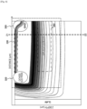
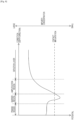
- a dark-state cathodic potential of the photodiode 300 is set as Vop.
- the photodiode 300 receives reflected light and performs avalanche amplification, a large current flows to the resistor 221 and voltage drop occurs.
- the cathodic potential decreases to a potential Vbd at which the avalanche amplification does not occur due to the voltage drop, the large current stops. This phenomenon is referred to as "quench.”
- Time from a point of time at which lowering a cathodic potential initiates to a point of time at which the cathodic potential returns to the potential Vop is time for which the photodiode 300 is not able to react with a photon, and is referred to as "dead time.”
- time from occurrence of avalanche amplification to occurrence of quench is very short, and thus a length of the dead time is approximately limited by a recharge time of the photodiode 300.
- Fig. 5 is an example of a plan view of the photodiode 300 according to the first embodiment of the present technology.
- a shape of the photodiode 300 is, for example, a rectangular shape when viewed from the Z direction.
- the anode electrode 310 is disposed along an outer edge of the photodiode 300.
- the cathode electrode 320 is disposed to be adjacent to an inner side of the anode electrode 310.
- the pinning region 330 is provided to be adjacent to an inner side of the cathode electrode 320.
- the contact 350 is disposed at the inside (the center and the like) of the pinning region 330.
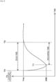
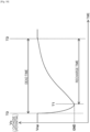
- the impurity concentration of the pinning region 330 is set to be equal to or greater than the impurity concentration of the contact 350, a potential barrier of the barrier region 340 is enlarged, and it is easy to suppress a leakage current.
- a difference in the impurity concentration between the pinning region 330 and the cathode electrode 320 increases, and the depletion layer width therebetween becomes narrower, and thus the pixel capacity C increases.
- Time from the timing T0 at which lowering of the cathodic potential initiates to the timing T2 at which the cathodic potential returns to the potential Vop corresponds to the dead time.
- a length of the dead time is mostly limited by a recharge time from the timing T1 to the timing T2.
- Fig. 12 is an example of a cross-sectional view of the photodiode 300 after mounting the substrate according to the first embodiment of the present technology.
- the anode electrode 310, the cathode electrode 320, and the contact 350 are connected to substrates 401 and 402 through a signal line.
- Fig. 13 is an example of a cross-sectional view of the photodiode before forming an insulating region according to the first embodiment of the present technology. After connecting the substrates 401 and 402, the light-receiving surface is polished by a polishing device 410.
- Fig. 14 is an example of a cross-sectional view of the photodiode after forming the insulating region according to the first embodiment of the present technology. After the polishing, the insulating region 380 is formed in the vicinity of an outer edge of the photodiode 300 and pixels are isolated.
- the impurity concentration of the pinning region 330 is set to be lower than that of the contact 350.
- the potential barrier further decreases in comparison to a case where the impurity concentration is set to be equal to or greater than the impurity concentration of the contact 350. Accordingly, when a dark current increases, there is a concern that a hole in the dark current jumps over the potential barrier, and jumps to the amplification region 360.
- a photodiode 300 according to the second embodiment is different from the first embodiment in that the pixel capacity is reduced by a method other than adjustment of the impurity concentration of the pinning region 330.
- Fig. 17 is an example of a cross-sectional view of the photodiode 300 according to the second embodiment of the present technology.
- the photodiode 300 of the second embodiment is different from the first embodiment in that the contact 350 is connected to the cathode electrode 320 through a signal line. According to this, a cathodic potential is applied to the contact 350, and a potential difference between the contact 350 and the cathode electrode 320 does not exist. Accordingly, the pixel capacity C of the photodiode 300 is further reduced in comparison to the first embodiment from the viewpoint of a circuit connected to the photodiode 300.
- cathode electrode 320 and the contact 350 are an example of a pair of electrodes described in the appended claims.
- the same potential is applied to the cathode electrode 320 and the contact 350, and thus it is possible to further reduce the pixel capacity in comparison to a case where potentials different from each are applied thereto.
- the pinning region 330 is formed in the photodiode 300 through ion implantation.
- a defect damage may occur on a substrate the photodiode 300 is formed due to the ion implantation.
- a third embodiment is different from the first embodiment in that a semiconductor layer of a metal oxide semiconductor (MOS) transistor adjacent to the photodiode 300 is used as the pinning region.
- MOS metal oxide semiconductor
- Fig. 18 is an example of a cross-sectional view of a pixel circuit 220 according to the third embodiment of the present technology.
- the pixel circuit 220 of the third embodiment further includes a transistor 390.
- the pinning region 330 is not formed in the photodiode 300.
- the transistor 390 is a MOS transistor including a metal layer 391, an oxide film 392, and a semiconductor layer 393.
- the semiconductor layer 393 is provided on an upper side of the barrier region 340 of the photodiode 300, and the oxide film 392 is formed on an upper side of the semiconductor layer 393.
- the metal layer 391 is provided on an upper side of the oxide film 392.
- the metal layer 391 can be used as a gate of the transistor 390, and a source and a drain are formed in the semiconductor layer 393.
- a negative bias lower than a reference potential is applied to the gate of the transistor 390. According to this, it is possible to suppress a dark current by inducing a hole in the dark current. That is, the semiconductor layer 393 functions as a pinning region.
- impurities for pinning may not be added to a silicon surface of the photodiode 300, and thus it is possible to remove a defect damage due to addition of the impurities.
- an interface level is lowered, and thus it is possible to lower the DCR. According to this, it is possible to raise a potential of the pinning region (semiconductor layer 393) to a certain extent corresponding to lowering of the DCR due to lowering of the interface level. As a result, it is possible to further reduce the pixel capacity C in comparison to the first embodiment.
- the dark current is suppressed by applying a negative bias to the gate electrode of the transistor 390, it is not necessary to form the pinning region in the photodiode 300. According to this, it is possible to remove the defect damage of the photodiode 300 due to formation of the pinning region.
- Fig. 19 is an example of a plan view of the photodiode 300 according to the fourth embodiment of the present technology.
- the cathode electrode 320 is disposed on an inner side (the center and the like) of the pinning region 330 when viewed from the Z direction.
- the contact 350 is disposed at the periphery of the pinning region 330.
- the cathode electrode 320 is disposed on an inner side of the pinning region 330, it is possible to further shorten the junction portion in comparison to a case where the cathode electrode 320 is disposed at the periphery of the pinning region 330. According to this, it is possible to reduce the electrostatic capacity of the pixel circuit 220.
- the shape of the photodiode 300 is set to a rectangular shape.
- an intense electric field is likely to occur at an end of the photodiode 300, and thus avalanche amplification occurs at the outside of the amplification region 360, and thus there is a concern that an operation of the pixel circuit 220 is blocked.
- This phenomenon is referred to as an edge breakdown phenomenon.
- the fifth embodiment is different from the first embodiment in that the shape of the photodiode 300 is set to a circular shape.
- Fig. 20 is an example of a plan view of the photodiode 300 according to the fifth embodiment of the present technology.
- the photodiode 300 of the fifth embodiment is different from the first embodiment in that a shape on a plane parallel to the light-receiving surface is set to a circular shape.
- Shapes of the cathode electrode 320, the pinning region 330, and the contact 350 in the photodiode 300 are also set to a circular shape.
- the shape of the photodiode 300 When the shape of the photodiode 300 is set to a circular shape, an effective area of the amplification region 360 decreases, and thus there is a possibility that an occurrence probability (photon detection efficiency (PDE)) of avalanche amplification with respect to one photon decreases.
- PDE photon detection efficiency
- an intense electric field is less likely to occur at an end of the photodiode 300, and thus it is possible to suppress the edge breakdown phenomenon. In addition, it is possible to enhance long-term reliability.
- the shape of the photodiode 300 is set to the circular shape, but a polygonal shape such as a pentagon and a hexagon close to a circle may be employed.
- the shape of the photodiode 300 is set to a circular shape, and thus an edge disappears. As a result, it is possible to suppress the edge breakdown phenomenon.
- the technology (the present technology) according to the present disclosure is applicable to various products.
- the technology according to the present disclosure can be realized as a device that is mounted on a moving body any one kind among an automobile, an electric vehicle, a hybrid electric vehicle, a motorcycle, a bicycle, a personal mobility, an airplane, a drone, a ship, a robot, and the like.
- Fig. 21 is a block diagram illustrating a schematic configuration example of a vehicle control system that is an example of a moving body control system to which the technology according to the present disclosure is applicable.
- a vehicle control system 12000 includes a plurality of electronic control units which are connected to each other through a communication network 12001.
- the vehicle control system 12000 includes a drive system control unit 12010, a body system control unit 12020, a vehicle exterior information detection unit 12030, a vehicle interior information detection unit 12040, and an integrated control unit 12050.
- a microcomputer 12051, a voice and image output unit 12052, and an in-vehicle network interface (I/F) 12053 are illustrated in the drawing.
- the drive system control unit 12010 controls an operation of a device relating to the drive system of the vehicle in accordance with various programs.
- the drive system control unit 12010 functions as a control device of a drive force generation device such as an internal combustion engine and a drive motor which generate a drive force of the vehicle, a drive force transmission mechanism that transmits the drive force to wheels, a steering mechanism that adjusts a steering angle of the vehicle, and a braking device that generates a braking force of the vehicle, and the like.
- the body system control unit 12020 controls an operation of various devices which are mounted to a vehicle body in accordance with various programs.
- the body system control unit 12020 functions as a control device of a keyless entry system, a smart key system, a power window device, and various lamps such as a head lamp, a back lamp, a brake lamp, a winker, and a fog lamp.
- an electric wave that is transmitted from a portable device that substitutes for a key, or signals of various switches can be input to the body system control unit 12020.
- the body system control unit 12020 receives input of the electric wave or the signals, and controls a door lock device, a power window device, a lamp, and the like of the vehicle.
- the vehicle exterior information detection unit 12030 detects information on an outer side of the vehicle on which the vehicle control system 12000 is mounted. For example, an imaging unit 12031 is connected to the vehicle exterior information detection unit 12030. The vehicle exterior information detection unit 12030 allows the imaging unit 12031 to capture a vehicle exterior image, and receives the captured image. The vehicle exterior information detection unit 12030 may perform object detection processing of a person, a vehicle, an obstacle, a sign, a character on a road, or the like, or distance detection processing on the basis of the image that is received.
- the imaging unit 12031 is an optical sensor that receives light and outputs an electric signal corresponding to the amount of light received.
- the imaging unit 12031 can output the electric signal as an image or as distance measurement information.
- light received by the imaging unit 12031 may be visible light, or invisible light such as infrared rays.
- the vehicle interior information detection unit 12040 detects vehicle interior information.
- a driver state detection unit 12041 that detects a driver state is connected to the vehicle interior information detection unit 12040.
- the driver state detection unit 12041 includes a camera that images a driver, and the vehicle interior information detection unit 12040 may calculate the degree of fatigue or the degree of concentration of a driver, or may determine whether or not the driver drowses on the basis of detection information that is input from the driver state detection unit 12041.
- the microcomputer 12051 calculates a control target value of the drive force generation device, the steering mechanism, or the braking device on the basis of vehicle interior or exterior information that is acquired by the vehicle exterior information detection unit 12030 or the vehicle interior information detection unit 12040, and can output a control command to the drive system control unit 12010.
- the microcomputer 12051 can perform a cooperative control to realize a function of an advanced driver assistance system (ADAS) which includes collision avoidance or impact mitigation of the vehicle, following travel based on an inter-vehicle distance, vehicle speed maintenance travel, vehicle collision alarm, vehicle lane deviation alarm, and the like.
- ADAS advanced driver assistance system
- the microcomputer 12051 can perform a cooperative control for automatic driving and the like in which the vehicle autonomously travels without depending on an operation of a driver by controlling the drive force generation device, the steering mechanism, the braking device, and the like on the basis of information in the vicinity of the vehicle which is acquired by the vehicle exterior information detection unit 12030 or the vehicle interior information detection unit 12040.
- the microcomputer 12051 can output a control command to the body system control unit 12020 on the basis of the vehicle exterior information acquired by the vehicle exterior information detection unit 12030.
- the microcomputer 12051 can perform a cooperative control to realize glare protection such as switching of a high beam into a low beam by controlling the head lamp in correspondence with a position of a preceding vehicle or an oncoming vehicle which is detected by the vehicle exterior information detection unit 12030.
- the voice and image output unit 12052 transmits at least one output signal between a voice and an image to an output device capable of visually or aurally notifying a passenger in a vehicle or an outer side of the vehicle of information.
- an audio speaker 12061, a display unit 12062, and an instrument panel 12063 are exemplified.
- the display unit 12062 may include at least one of an on-board display and a head-up display.
- Fig. 22 is a view illustrating an example of an installation position of the imaging unit 12031.
- imaging units 12101, 12102, 12103, 12104, and 12105 are provided.
- the imaging units 12101, 12102, 12103, 12104, and 12105 are installed at positions such as a front nose, a side-view mirror, a rear bumper, a back door, an upper side of a vehicle front glass in a vehicle room, of the vehicle 12100.
- the imaging unit 12101 provided at the front nose, and the imaging unit 12105 that is provided on an upper side of the vehicle front glass in a vehicle room mainly acquire images on a forward side of the vehicle 12100.
- the imaging units 12102 and 12103 which are provided in the side-view mirror mainly acquire images on a lateral side of the vehicle 12100.
- the imaging unit 12104 that is provided in the rear bumper or the back door mainly acquires images on a backward side of the vehicle 12100.
- the imaging unit 12105 that is provided on an upper side of the vehicle front glass in the vehicle room can be mainly used to detect a preceding vehicle, a pedestrian, an obstacle, a traffic signal, a traffic sign, a vehicle lane, and the like.
- Fig. 22 illustrates an example of a photographing range of the imaging units 12101 to 12104.
- An image capturing range 12111 represents an image capturing range of the imaging unit 12101 that is provided in the front nose
- image capturing ranges 12112 and 12113 respectively represent image capturing ranges of the imaging units 12102 and 12103 which are provided in the side-view mirrors
- an image capturing range 12114 represents an image capturing range of the imaging unit 12104 that is provided in the rear bumper or the back door.
- At least one of the imaging units 12101 to 12104 may have a function of acquiring distance information.
- at least one of the imaging units 12101 to 12104 may be a stereo camera including a plurality of imaging elements, or may be an imaging element that includes pixels for phase difference detection.
- the microcomputer 12051 can extract a three-dimensional object, which is a closest three-dimensional object, particularly, on a proceeding path of the vehicle 12100 and travels in approximately the same direction as that of the vehicle 12100 that travels at a predetermined velocity (for example, 0 km/h or greater), as a preceding vehicle by obtaining distances to respective three-dimensional objects in the image capturing ranges 12111 to 12114 and a variation of the distances with the passage of time (relative velocity to the vehicle 12100) on the basis of the distance information obtained from the imaging units 12101 to 12104.
- a predetermined velocity for example, 0 km/h or greater
- the microcomputer 12051 can set a distance between vehicles to be secured in advance in front of the preceding vehicle to perform automatic brake control (also including a following stop control), an automatic acceleration control (also including a following acceleration control), and the like. As described above, it is possible to perform a cooperative control for automatic driving in which a vehicle autonomously travels without depending on an operation by a driver, and the like.
- the microcomputer 12051 can extract three-dimensional object data relating to a three-dimensional object by classifying a plurality of pieces of the three-dimensional object data into data of a two-wheel vehicle, data of typical vehicle, data of a large-sized vehicle, data of pedestrian, and data of other three-dimensional objects such as an electric pole on the basis of the distance information obtained from the imaging units 12101 to 12104, and can use the three-dimensional object data for automatic obstacle avoidance.
- the microcomputer 12051 discriminates obstacles at the periphery of the vehicle 12100 into an obstacle that is visually recognized by a driver of the vehicle 12100 and an obstacle that is difficult to be visually recognized by the driver.
- the microcomputer 12051 determines collision risk indicating the degree of danger of collision with each of the obstacles.
- the microcomputer 12051 can assist driving for collision avoidance by outputting an alarm to the driver through the audio speaker 12061 or the display unit 12062, or by performing compulsory deceleration or avoidance steering through the drive system control unit 12010.
- At least one of the imaging units 12101 to 12104 may be an infrared camera that detects infrared rays.
- the microcomputer 12051 can recognize a pedestrian by determining whether or not the pedestrian exists in image captured by the imaging units 12101 to 12104.
- the pedestrian recognition is performed by a procedure of extracting a specific point in images captured by the imaging units 12101 to 12104 as an infrared camera, and a procedure of performing pattern matching processing for a series of specific points indicating a contour line of an object to determine whether or not the object is a pedestrian.
- the voice and image output unit 12052 controls the display unit 12062 to overlap and display a quadrangular contour line for emphasis on the pedestrian who is recognized.
- the voice and image output unit 12052 may control the display unit 12062 to display an icon and the like indicating the pedestrian at a desired position.
- the technology relating to the present disclosure is applicable to, for example, the vehicle exterior information detection unit 12030 among the above-described configurations.
- the distance measurement module 100 in Fig. 1 is applicable to the vehicle exterior information detection unit 12030 in Fig. 21 .
- the technology relating to the present disclosure is applied to the vehicle exterior information detection unit 12030, a dark current is suppressed, and thus accurate distance data can be obtained. Accordingly, it is possible to improve reliability of a vehicle control system.
Landscapes
- Physics & Mathematics (AREA)
- General Physics & Mathematics (AREA)
- Spectroscopy & Molecular Physics (AREA)
- Solid State Image Pick-Up Elements (AREA)
- Light Receiving Elements (AREA)
- Optical Radar Systems And Details Thereof (AREA)
- Transforming Light Signals Into Electric Signals (AREA)
Applications Claiming Priority (2)
| Application Number | Priority Date | Filing Date | Title |
|---|---|---|---|
| JP2017206729A JP6860467B2 (ja) | 2017-10-26 | 2017-10-26 | フォトダイオード、画素回路、および、フォトダイオードの製造方法 |
| PCT/JP2018/032637 WO2019082513A1 (en) | 2017-10-26 | 2018-09-03 | AVALANCHE PHOTODIODE SENSOR |
Publications (2)
| Publication Number | Publication Date |
|---|---|
| EP3545559A1 EP3545559A1 (en) | 2019-10-02 |
| EP3545559B1 true EP3545559B1 (en) | 2024-11-27 |
Family
ID=63638247
Family Applications (1)
| Application Number | Title | Priority Date | Filing Date |
|---|---|---|---|
| EP18772919.9A Active EP3545559B1 (en) | 2017-10-26 | 2018-09-03 | Avalanche photodiode sensor |
Country Status (6)
Families Citing this family (9)
| Publication number | Priority date | Publication date | Assignee | Title |
|---|---|---|---|---|
| JP7445397B2 (ja) * | 2019-07-31 | 2024-03-07 | ソニーセミコンダクタソリューションズ株式会社 | 受光素子および電子機器 |
| JP7362352B2 (ja) | 2019-08-23 | 2023-10-17 | キヤノン株式会社 | 光電変換装置、光電変換システム、および移動体 |
| US11374135B2 (en) | 2019-08-30 | 2022-06-28 | Globalfoundries Singapore Pte. Ltd. | Sensor and method of forming the same |
| US20230048727A1 (en) * | 2019-12-26 | 2023-02-16 | Hamamatsu Photonics K.K. | Ranging image sensor |
| CN114902418A (zh) * | 2019-12-26 | 2022-08-12 | 浜松光子学株式会社 | 测距图像传感器及其制造方法 |
| KR20210121851A (ko) * | 2020-03-31 | 2021-10-08 | 에스케이하이닉스 주식회사 | 이미지 센싱 장치 |
| CN114124212A (zh) * | 2020-08-26 | 2022-03-01 | 华为技术有限公司 | 一种分光探测器及光纤通信系统 |
| JP2022054553A (ja) * | 2020-09-28 | 2022-04-07 | ソニーセミコンダクタソリューションズ株式会社 | 固体撮像素子、および、撮像装置 |
| CN116400370A (zh) * | 2022-05-30 | 2023-07-07 | 神盾股份有限公司 | 距离感测装置及其感测方法 |
Family Cites Families (13)
| Publication number | Priority date | Publication date | Assignee | Title |
|---|---|---|---|---|
| JP5015494B2 (ja) * | 2006-05-22 | 2012-08-29 | 住友電工デバイス・イノベーション株式会社 | 半導体受光素子 |
| WO2008113067A2 (en) | 2007-03-15 | 2008-09-18 | Johns Hopkins University | Deep submicron and nano cmos single photon photodetector pixel with event based circuits for readout data-rate reduction |
| ITTO20080046A1 (it) * | 2008-01-18 | 2009-07-19 | St Microelectronics Srl | Schiera di fotodiodi operanti in modalita' geiger reciprocamente isolati e relativo procedimento di fabbricazione |
| JP5631668B2 (ja) * | 2010-09-02 | 2014-11-26 | Nttエレクトロニクス株式会社 | アバランシ・フォトダイオード |
| CN102184929B (zh) * | 2011-03-24 | 2013-04-24 | 南京大学 | 紫外光雪崩管成像阵列像元、其应用方法及雪崩管成像阵列 |
| JP5508356B2 (ja) * | 2011-07-26 | 2014-05-28 | シャープ株式会社 | 固体撮像装置およびその駆動方法、固体撮像装置の製造方法、並びに電子情報機器 |
| JP5926921B2 (ja) * | 2011-10-21 | 2016-05-25 | 浜松ホトニクス株式会社 | 光検出装置 |
| JP6090060B2 (ja) * | 2013-08-23 | 2017-03-08 | 株式会社豊田中央研究所 | シングルフォトンアバランシェダイオード |
| WO2015120583A1 (zh) * | 2014-02-12 | 2015-08-20 | 华为技术有限公司 | 一种雪崩光电二极管及其制造方法 |
| JP6260917B2 (ja) * | 2014-07-25 | 2018-01-17 | パナソニックIpマネジメント株式会社 | フォトダイオード、フォトダイオードアレイ、及び固体撮像素子 |
| JP6362478B2 (ja) * | 2014-08-27 | 2018-07-25 | ルネサスエレクトロニクス株式会社 | 半導体装置の製造方法および半導体装置 |
| WO2017169122A1 (ja) * | 2016-03-30 | 2017-10-05 | ソニー株式会社 | 光電変換素子および光電変換装置 |
| KR102625899B1 (ko) * | 2017-03-22 | 2024-01-18 | 소니 세미컨덕터 솔루션즈 가부시키가이샤 | 촬상 장치 및 신호 처리 장치 |
-
2017
- 2017-10-26 JP JP2017206729A patent/JP6860467B2/ja active Active
-
2018
- 2018-09-03 KR KR1020207010621A patent/KR20200063160A/ko not_active Withdrawn
- 2018-09-03 KR KR1020197015450A patent/KR102103128B1/ko active Active
- 2018-09-03 EP EP18772919.9A patent/EP3545559B1/en active Active
- 2018-09-03 CN CN201880004684.9A patent/CN110036491B/zh active Active
- 2018-09-03 US US16/462,471 patent/US11333549B2/en active Active
- 2018-09-03 WO PCT/JP2018/032637 patent/WO2019082513A1/en unknown
Also Published As
| Publication number | Publication date |
|---|---|
| US11333549B2 (en) | 2022-05-17 |
| KR20200063160A (ko) | 2020-06-04 |
| WO2019082513A1 (en) | 2019-05-02 |
| KR102103128B1 (ko) | 2020-04-21 |
| EP3545559A1 (en) | 2019-10-02 |
| US20200249083A1 (en) | 2020-08-06 |
| JP2019079968A (ja) | 2019-05-23 |
| CN110036491B (zh) | 2024-02-13 |
| CN110036491A (zh) | 2019-07-19 |
| JP6860467B2 (ja) | 2021-04-14 |
| KR20190109388A (ko) | 2019-09-25 |
Similar Documents
| Publication | Publication Date | Title |
|---|---|---|
| EP3545559B1 (en) | Avalanche photodiode sensor | |
| US11950010B2 (en) | Imaging apparatus and imaging system | |
| JP7445397B2 (ja) | 受光素子および電子機器 | |
| EP3721483B1 (en) | Avalanche photodiode sensor, and electronic device | |
| US11849200B2 (en) | Light-receiving device, imaging device, and distance measurement device for expanded range of photon detection efficiency | |
| US20200382737A1 (en) | Solid-state imaging device, electronic device, and controlling method of solid-state imaging device | |
| US20240072192A1 (en) | Optical detection device | |
| US20220384493A1 (en) | Solid-state imaging apparatus and distance measurement system | |
| WO2022113733A1 (ja) | 受光素子、測距システム、および、電子機器 | |
| US20250040269A1 (en) | Photodetection device and distance measuring system | |
| US12349494B2 (en) | Light receiving device and distance measuring device | |
| US20210399032A1 (en) | Light reception element and electronic apparatus | |
| US20240072080A1 (en) | Light detection device and distance measurement apparatus | |
| JP7583788B2 (ja) | 固体撮像素子、および、電子装置 | |
| US20250199137A1 (en) | Photodetector and distance measurement apparatus | |
| US20230053574A1 (en) | Solid-state imaging element, imaging device, and method for controlling solid-state imaging element | |
| WO2025088776A1 (ja) | 受光素子、測距システム | |
| CN119547584A (zh) | 光检测器和距离测量设备 |
Legal Events
| Date | Code | Title | Description |
|---|---|---|---|
| STAA | Information on the status of an ep patent application or granted ep patent |
Free format text: STATUS: UNKNOWN |
|
| STAA | Information on the status of an ep patent application or granted ep patent |
Free format text: STATUS: THE INTERNATIONAL PUBLICATION HAS BEEN MADE |
|
| PUAI | Public reference made under article 153(3) epc to a published international application that has entered the european phase |
Free format text: ORIGINAL CODE: 0009012 |
|
| STAA | Information on the status of an ep patent application or granted ep patent |
Free format text: STATUS: REQUEST FOR EXAMINATION WAS MADE |
|
| 17P | Request for examination filed |
Effective date: 20190626 |
|
| AK | Designated contracting states |
Kind code of ref document: A1 Designated state(s): AL AT BE BG CH CY CZ DE DK EE ES FI FR GB GR HR HU IE IS IT LI LT LU LV MC MK MT NL NO PL PT RO RS SE SI SK SM TR |
|
| AX | Request for extension of the european patent |
Extension state: BA ME |
|
| DAV | Request for validation of the european patent (deleted) | ||
| DAX | Request for extension of the european patent (deleted) | ||
| STAA | Information on the status of an ep patent application or granted ep patent |
Free format text: STATUS: EXAMINATION IS IN PROGRESS |
|
| 17Q | First examination report despatched |
Effective date: 20211221 |
|
| GRAP | Despatch of communication of intention to grant a patent |
Free format text: ORIGINAL CODE: EPIDOSNIGR1 |
|
| STAA | Information on the status of an ep patent application or granted ep patent |
Free format text: STATUS: GRANT OF PATENT IS INTENDED |
|
| INTG | Intention to grant announced |
Effective date: 20240102 |
|
| GRAJ | Information related to disapproval of communication of intention to grant by the applicant or resumption of examination proceedings by the epo deleted |
Free format text: ORIGINAL CODE: EPIDOSDIGR1 |
|
| STAA | Information on the status of an ep patent application or granted ep patent |
Free format text: STATUS: EXAMINATION IS IN PROGRESS |
|
| INTC | Intention to grant announced (deleted) | ||
| GRAP | Despatch of communication of intention to grant a patent |
Free format text: ORIGINAL CODE: EPIDOSNIGR1 |
|
| STAA | Information on the status of an ep patent application or granted ep patent |
Free format text: STATUS: GRANT OF PATENT IS INTENDED |
|
| INTG | Intention to grant announced |
Effective date: 20240626 |
|
| GRAS | Grant fee paid |
Free format text: ORIGINAL CODE: EPIDOSNIGR3 |
|
| P01 | Opt-out of the competence of the unified patent court (upc) registered |
Free format text: CASE NUMBER: APP_52307/2024 Effective date: 20240918 |
|
| GRAA | (expected) grant |
Free format text: ORIGINAL CODE: 0009210 |
|
| STAA | Information on the status of an ep patent application or granted ep patent |
Free format text: STATUS: THE PATENT HAS BEEN GRANTED |
|
| REG | Reference to a national code |
Ref country code: DE Ref legal event code: R079 Ref document number: 602018077003 Country of ref document: DE Free format text: PREVIOUS MAIN CLASS: H01L0031035200 Ipc: H10F0077140000 |
|
| AK | Designated contracting states |
Kind code of ref document: B1 Designated state(s): AL AT BE BG CH CY CZ DE DK EE ES FI FR GB GR HR HU IE IS IT LI LT LU LV MC MK MT NL NO PL PT RO RS SE SI SK SM TR |
|
| REG | Reference to a national code |
Ref country code: GB Ref legal event code: FG4D |
|
| REG | Reference to a national code |
Ref country code: CH Ref legal event code: EP |
|
| REG | Reference to a national code |
Ref country code: IE Ref legal event code: FG4D |
|
| REG | Reference to a national code |
Ref country code: DE Ref legal event code: R096 Ref document number: 602018077003 Country of ref document: DE |
|
| REG | Reference to a national code |
Ref country code: NL Ref legal event code: FP |
|
| REG | Reference to a national code |
Ref country code: LT Ref legal event code: MG9D |
|
| PG25 | Lapsed in a contracting state [announced via postgrant information from national office to epo] |
Ref country code: HR Free format text: LAPSE BECAUSE OF FAILURE TO SUBMIT A TRANSLATION OF THE DESCRIPTION OR TO PAY THE FEE WITHIN THE PRESCRIBED TIME-LIMIT Effective date: 20241127 Ref country code: IS Free format text: LAPSE BECAUSE OF FAILURE TO SUBMIT A TRANSLATION OF THE DESCRIPTION OR TO PAY THE FEE WITHIN THE PRESCRIBED TIME-LIMIT Effective date: 20250327 Ref country code: PT Free format text: LAPSE BECAUSE OF FAILURE TO SUBMIT A TRANSLATION OF THE DESCRIPTION OR TO PAY THE FEE WITHIN THE PRESCRIBED TIME-LIMIT Effective date: 20250327 |
|
| PG25 | Lapsed in a contracting state [announced via postgrant information from national office to epo] |
Ref country code: FI Free format text: LAPSE BECAUSE OF FAILURE TO SUBMIT A TRANSLATION OF THE DESCRIPTION OR TO PAY THE FEE WITHIN THE PRESCRIBED TIME-LIMIT Effective date: 20241127 |
|
| REG | Reference to a national code |
Ref country code: AT Ref legal event code: MK05 Ref document number: 1746601 Country of ref document: AT Kind code of ref document: T Effective date: 20241127 |
|
| PG25 | Lapsed in a contracting state [announced via postgrant information from national office to epo] |
Ref country code: BG Free format text: LAPSE BECAUSE OF FAILURE TO SUBMIT A TRANSLATION OF THE DESCRIPTION OR TO PAY THE FEE WITHIN THE PRESCRIBED TIME-LIMIT Effective date: 20241127 |
|
| PG25 | Lapsed in a contracting state [announced via postgrant information from national office to epo] |
Ref country code: ES Free format text: LAPSE BECAUSE OF FAILURE TO SUBMIT A TRANSLATION OF THE DESCRIPTION OR TO PAY THE FEE WITHIN THE PRESCRIBED TIME-LIMIT Effective date: 20241127 |
|
| PG25 | Lapsed in a contracting state [announced via postgrant information from national office to epo] |
Ref country code: NO Free format text: LAPSE BECAUSE OF FAILURE TO SUBMIT A TRANSLATION OF THE DESCRIPTION OR TO PAY THE FEE WITHIN THE PRESCRIBED TIME-LIMIT Effective date: 20250227 |
|
| PG25 | Lapsed in a contracting state [announced via postgrant information from national office to epo] |
Ref country code: LV Free format text: LAPSE BECAUSE OF FAILURE TO SUBMIT A TRANSLATION OF THE DESCRIPTION OR TO PAY THE FEE WITHIN THE PRESCRIBED TIME-LIMIT Effective date: 20241127 Ref country code: GR Free format text: LAPSE BECAUSE OF FAILURE TO SUBMIT A TRANSLATION OF THE DESCRIPTION OR TO PAY THE FEE WITHIN THE PRESCRIBED TIME-LIMIT Effective date: 20250228 Ref country code: AT Free format text: LAPSE BECAUSE OF FAILURE TO SUBMIT A TRANSLATION OF THE DESCRIPTION OR TO PAY THE FEE WITHIN THE PRESCRIBED TIME-LIMIT Effective date: 20241127 |
|
| PG25 | Lapsed in a contracting state [announced via postgrant information from national office to epo] |
Ref country code: PL Free format text: LAPSE BECAUSE OF FAILURE TO SUBMIT A TRANSLATION OF THE DESCRIPTION OR TO PAY THE FEE WITHIN THE PRESCRIBED TIME-LIMIT Effective date: 20241127 |
|
| PG25 | Lapsed in a contracting state [announced via postgrant information from national office to epo] |
Ref country code: RS Free format text: LAPSE BECAUSE OF FAILURE TO SUBMIT A TRANSLATION OF THE DESCRIPTION OR TO PAY THE FEE WITHIN THE PRESCRIBED TIME-LIMIT Effective date: 20250227 |
|
| PG25 | Lapsed in a contracting state [announced via postgrant information from national office to epo] |
Ref country code: SM Free format text: LAPSE BECAUSE OF FAILURE TO SUBMIT A TRANSLATION OF THE DESCRIPTION OR TO PAY THE FEE WITHIN THE PRESCRIBED TIME-LIMIT Effective date: 20241127 |
|
| PG25 | Lapsed in a contracting state [announced via postgrant information from national office to epo] |
Ref country code: DK Free format text: LAPSE BECAUSE OF FAILURE TO SUBMIT A TRANSLATION OF THE DESCRIPTION OR TO PAY THE FEE WITHIN THE PRESCRIBED TIME-LIMIT Effective date: 20241127 |
|
| PG25 | Lapsed in a contracting state [announced via postgrant information from national office to epo] |
Ref country code: EE Free format text: LAPSE BECAUSE OF FAILURE TO SUBMIT A TRANSLATION OF THE DESCRIPTION OR TO PAY THE FEE WITHIN THE PRESCRIBED TIME-LIMIT Effective date: 20241127 |
|
| PG25 | Lapsed in a contracting state [announced via postgrant information from national office to epo] |
Ref country code: RO Free format text: LAPSE BECAUSE OF FAILURE TO SUBMIT A TRANSLATION OF THE DESCRIPTION OR TO PAY THE FEE WITHIN THE PRESCRIBED TIME-LIMIT Effective date: 20241127 |
|
| PG25 | Lapsed in a contracting state [announced via postgrant information from national office to epo] |
Ref country code: SK Free format text: LAPSE BECAUSE OF FAILURE TO SUBMIT A TRANSLATION OF THE DESCRIPTION OR TO PAY THE FEE WITHIN THE PRESCRIBED TIME-LIMIT Effective date: 20241127 |
|
| PG25 | Lapsed in a contracting state [announced via postgrant information from national office to epo] |
Ref country code: CZ Free format text: LAPSE BECAUSE OF FAILURE TO SUBMIT A TRANSLATION OF THE DESCRIPTION OR TO PAY THE FEE WITHIN THE PRESCRIBED TIME-LIMIT Effective date: 20241127 |
|
| PG25 | Lapsed in a contracting state [announced via postgrant information from national office to epo] |
Ref country code: IT Free format text: LAPSE BECAUSE OF FAILURE TO SUBMIT A TRANSLATION OF THE DESCRIPTION OR TO PAY THE FEE WITHIN THE PRESCRIBED TIME-LIMIT Effective date: 20241127 |