EP3512318B1 - Heat dissipation structure for electronic device, and electronic device - Google Patents
Heat dissipation structure for electronic device, and electronic device Download PDFInfo
- Publication number
- EP3512318B1 EP3512318B1 EP17854914.3A EP17854914A EP3512318B1 EP 3512318 B1 EP3512318 B1 EP 3512318B1 EP 17854914 A EP17854914 A EP 17854914A EP 3512318 B1 EP3512318 B1 EP 3512318B1
- Authority
- EP
- European Patent Office
- Prior art keywords
- heat
- layer
- contact
- region
- speaker box
- Prior art date
- Legal status (The legal status is an assumption and is not a legal conclusion. Google has not performed a legal analysis and makes no representation as to the accuracy of the status listed.)
- Active
Links
- 230000017525 heat dissipation Effects 0.000 title claims description 66
- 239000000853 adhesive Substances 0.000 claims description 44
- 230000001070 adhesive effect Effects 0.000 claims description 44
- 239000004020 conductor Substances 0.000 claims description 31
- 238000003466 welding Methods 0.000 claims description 28
- 238000009413 insulation Methods 0.000 claims description 19
- 239000000463 material Substances 0.000 claims description 16
- 239000006260 foam Substances 0.000 claims description 6
- 239000002184 metal Substances 0.000 claims description 6
- 229910052751 metal Inorganic materials 0.000 claims description 6
- 239000000919 ceramic Substances 0.000 claims description 4
- 239000004033 plastic Substances 0.000 claims description 4
- 230000004907 flux Effects 0.000 description 10
- 238000012546 transfer Methods 0.000 description 9
- 238000004891 communication Methods 0.000 description 8
- 238000010586 diagram Methods 0.000 description 8
- 230000005855 radiation Effects 0.000 description 8
- 239000011347 resin Substances 0.000 description 4
- 229920005989 resin Polymers 0.000 description 4
- 238000005516 engineering process Methods 0.000 description 3
- 230000020169 heat generation Effects 0.000 description 3
- 238000012545 processing Methods 0.000 description 3
- 230000008859 change Effects 0.000 description 2
- 230000000694 effects Effects 0.000 description 2
- 238000000034 method Methods 0.000 description 2
- 238000010295 mobile communication Methods 0.000 description 2
- 230000008569 process Effects 0.000 description 2
- OKTJSMMVPCPJKN-UHFFFAOYSA-N Carbon Chemical compound [C] OKTJSMMVPCPJKN-UHFFFAOYSA-N 0.000 description 1
- RYGMFSIKBFXOCR-UHFFFAOYSA-N Copper Chemical compound [Cu] RYGMFSIKBFXOCR-UHFFFAOYSA-N 0.000 description 1
- 239000002131 composite material Substances 0.000 description 1
- 238000001816 cooling Methods 0.000 description 1
- 239000011889 copper foil Substances 0.000 description 1
- 238000011161 development Methods 0.000 description 1
- 229910002804 graphite Inorganic materials 0.000 description 1
- 239000010439 graphite Substances 0.000 description 1
- 238000005338 heat storage Methods 0.000 description 1
- 239000012774 insulation material Substances 0.000 description 1
- 239000012782 phase change material Substances 0.000 description 1
Images


Classifications
-
- H—ELECTRICITY
- H05—ELECTRIC TECHNIQUES NOT OTHERWISE PROVIDED FOR
- H05K—PRINTED CIRCUITS; CASINGS OR CONSTRUCTIONAL DETAILS OF ELECTRIC APPARATUS; MANUFACTURE OF ASSEMBLAGES OF ELECTRICAL COMPONENTS
- H05K7/00—Constructional details common to different types of electric apparatus
- H05K7/20—Modifications to facilitate cooling, ventilating, or heating
- H05K7/2039—Modifications to facilitate cooling, ventilating, or heating characterised by the heat transfer by conduction from the heat generating element to a dissipating body
- H05K7/20509—Multiple-component heat spreaders; Multi-component heat-conducting support plates; Multi-component non-closed heat-conducting structures
-
- H—ELECTRICITY
- H05—ELECTRIC TECHNIQUES NOT OTHERWISE PROVIDED FOR
- H05K—PRINTED CIRCUITS; CASINGS OR CONSTRUCTIONAL DETAILS OF ELECTRIC APPARATUS; MANUFACTURE OF ASSEMBLAGES OF ELECTRICAL COMPONENTS
- H05K7/00—Constructional details common to different types of electric apparatus
- H05K7/20—Modifications to facilitate cooling, ventilating, or heating
- H05K7/2039—Modifications to facilitate cooling, ventilating, or heating characterised by the heat transfer by conduction from the heat generating element to a dissipating body
- H05K7/20436—Inner thermal coupling elements in heat dissipating housings, e.g. protrusions or depressions integrally formed in the housing
- H05K7/20445—Inner thermal coupling elements in heat dissipating housings, e.g. protrusions or depressions integrally formed in the housing the coupling element being an additional piece, e.g. thermal standoff
- H05K7/20472—Sheet interfaces
-
- H—ELECTRICITY
- H05—ELECTRIC TECHNIQUES NOT OTHERWISE PROVIDED FOR
- H05K—PRINTED CIRCUITS; CASINGS OR CONSTRUCTIONAL DETAILS OF ELECTRIC APPARATUS; MANUFACTURE OF ASSEMBLAGES OF ELECTRICAL COMPONENTS
- H05K7/00—Constructional details common to different types of electric apparatus
- H05K7/20—Modifications to facilitate cooling, ventilating, or heating
- H05K7/2039—Modifications to facilitate cooling, ventilating, or heating characterised by the heat transfer by conduction from the heat generating element to a dissipating body
- H05K7/20518—Unevenly distributed heat load, e.g. different sectors at different temperatures, localised cooling, hot spots
Definitions
- Embodiments of this application relate to device dissipation technologies, and in particular, to a heat dissipation structure for an electronic device and an electronic device.
- a user may usually obtain a desired sound effect by increasing a volume of the electronic device.
- the volume of the electronic device is increased, power of a speaker box of the electronic device is increased undoubtedly. Consequently, the speaker box generates more heat.
- heat of another element adjacent to the speaker box inside the electronic device is conducted to the speaker box. Consequently, the speaker box also generates more heat.
- the speaker box in the electronic device has a poor heat conduction effect. Consequently, heat dissipation of the speaker box is poor. In this case, when the speaker box generates heat, the heat cannot be effectively conducted for dissipation. Consequently, a partial region of the speaker box in the electronic device overheats.
- US 2016/0109911 A1 discloses a solution to providing heat management and cooling to electronic devices.
- heat produced during the operation of the processing components in the computing device is absorbed by heat management features integrated within a supporting mid-frame.
- the heat management features include phase changing materials that allow the processing components to be kept at a isothermal state through changes in phase, thereby prolonging the duration of time in which the processing components can operate at high performance levels without the need to throttle the performance.
- CN 104601759 A discloses a cell phone heat radiation structure and a cell phone and relates to the technical field of the cell phones.
- the cell phone comprises a loudspeaker and receiver two-in-one front surface region, a main board region and an accessory region, wherein a camera region and an antenna region are arranged on the two sides of the loudspeaker and receiver two-in-one front surface region;
- the cell phone heat radiation structure comprises at least one heat radiation layer made of a heat radiation material; the heat radiation layer covers at least one part of the loudspeaker and receiver two-in-one front surface region and at least one part of the main board region.
- the invention further discloses the cell phone comprising the cell phone heat radiation structure.
- CN 2598039 A discloses an improved heat radiating structure for miniature trumpet inlayed thin material space.
- a heat radiating guide plate is arranged on rear metal base of internal inlay type miniature trumpet in thin material space of thin electronic products such as notebook, PDA and LCD, thus the heated metal base can transmit thermal energy to the heat radiating guide plate so as to enlarge heat radiation area of the miniature trumpet, prevent high temperature air concentrating in the miniature trumpet, strengthen heat radiation efficiency of the miniature trumpet, reduce temperature of voice coil inside the miniature trumpet, prevent the voice coil being burnt under high temperature, promote stability of outputted power, avoid hot air concentrating around the miniature trumpet aside shell of electronic product and prevent the shell of thin electronic product burning in high temperature.
- JP2009231907 A discloses a portable telephone device, capable of preventing a portion from being contacted by a user from becoming high temperature.
- the portable telephone device has an outer shell, formed by uniting a plurality of components, including a circuit board mounted with a plurality of electronic components, together with a resin member.
- a resin member As the resin member, a first resin member, having relatively high thermal conductivity, is used for the back side of a speaker where an ear of the user comes into contact with, and a second resin member having relatively low thermal conductivity is used for other portions.
- Embodiments of this application provide a heat dissipation structure for an electronic device and an electronic device, to avoid local high temperature of the electronic device.
- An embodiment of this application provides a heat dissipation structure for an electronic device, including: a rear cover, a mainboard, a battery, an antenna panel, a speaker box, and a middle frame, where a heat dissipating layer is disposed on the rear cover, a first shield cover and a second shield cover are disposed on the mainboard, and the speaker box is disposed on a surface of the antenna panel;
- the heat dissipation structure for an electronic device because the heat dissipating layer disposed on the rear cover may be in contact with the mainboard and the battery, and may also be in contact with the speaker box, the heat dissipation structure for an electronic device implements heat dissipation of the mainboard and the battery, and may further implement heat dissipation of a region of the speaker box, to effectively avoid local high temperature, and implement equalized heat dissipation of the electronic device, thereby improving user experience.
- the third region of the heat dissipating layer is in contact with a partial or entire region of the surface of the speaker box that is distant from the antenna panel.
- the third region of the heat dissipating layer is in contact with the surface of the speaker box that is distant from the antenna panel in an adhesive manner, and an adhesive used in the adhesive manner is an adhesive for heat conduction.
- the third region of the heat dissipating layer is in contact with the surface of the speaker box that is distant from the antenna panel in a welding manner.
- a material used in the adhesive manner or in the welding manner is a thermally conductive material, when the heat dissipating layer is in contact with the speaker box in the adhesive manner or in the welding manner, thermal conductivity between the heat dissipating layer and the speaker box may be improved, and heat transfer efficiency may be increased.
- the first region of the heat dissipating layer may also be in contact with the first shield cover of the mainboard in an adhesive manner or in a welding manner
- the second shield cover of the mainboard may also be in contact with the first region of the middle frame in an adhesive manner or in a welding manner.
- An adhesive used in the adhesive manner may also be an adhesive for heat conduction
- a flux used in the welding manner is a thermally conductive flux.
- a material used in the adhesive manner or in the welding manner is a thermally conductive material
- thermal conductivity between the heat dissipating layer and the first shield cover may be improved, thereby improving thermal conductivity between the mainboard and the heat dissipating layer, and increasing heat transfer efficiency.
- the second region of the heat dissipating layer may also be in contact with the battery in an adhesive manner or in a welding manner, and the another surface of the battery that is distant from the heat dissipating layer may also be in contact with the second region of middle frame in an adhesive manner or in a welding manner.
- An adhesive used in the adhesive manner may also be an adhesive for heat conduction, and a flux used in the welding manner is a thermally conductive flux.
- a material used in the adhesive manner or in the welding manner is a thermally conductive material, when the heat dissipating layer is in contact with the battery in the adhesive manner or in the welding manner, thermal conductivity between the heat dissipating layer and the battery may be improved, and heat transfer efficiency may be increased.
- a material of the speaker box is a thermally conductive material
- the thermally conductive material includes any one of the following: thermally conductive plastic, ceramic, and metal.
- heat generated by an element inside the speaker box may be better conducted to a surface of the speaker box, for effective dissipation.
- a dielectric constant of the thermally conductive material is less than or equal to 8
- a loss angle of the thermally conductive material is less than or equal to 0.01
- a coefficient of thermal conductivity of the thermally conductive material is greater than or equal to 1 W/(m ⁇ K).
- the dielectric constant of the thermally conductive material of the speaker box is less than or equal to 8, so that heat generated by an element inside the speaker box can be better conducted to a surface of the speaker box, to effectively avoid electrical interference from the element inside the speaker box.
- the coefficient of thermal conductivity of the thermally conductive material of the speaker box is greater than or equal to 1 W/(m ⁇ K), so that heat conductivity between the element inside the speaker box and the speaker box is improved, and heat transfer efficiency is increased.
- a charger is further disposed on the antenna panel.
- Heat generated by the charger in a charging process may be transferred to the speaker box by using the antenna panel, and then is dissipated by using the heat dissipating layer in contact with the speaker box. Heat dissipation of the region of the speaker box in a charging scenario may also be implemented, to avoid local high temperature of an electronic device, and improve user experience.
- the heat dissipating layer includes a heat equalizing layer, and the heat equalizing layer is in contact with the mainboard, the battery, and the antenna panel.
- the heat equalizing layer can evenly dissipate heat absorbed from the mainboard, the battery, and the speaker box, to effectively avoid local heat dissipation of the electronic device.
- a coefficient of thermal conductivity of the heat equalizing layer is greater than or equal to 250 W/(m ⁇ K).
- the heat dissipating layer further includes a heat accumulating layer and a heat insulation layer, the heat insulation layer is in contact with the rear cover, and the heat accumulating layer is located between the heat insulation layer and the heat equalizing layer.
- the heat accumulating layer can absorb heat from the heat equalizing layer by using a phase change, and stores heat energy, to alleviate temperature rise of the rear cover of the electronic device.
- the heat insulation layer can stop heat from being directly transferred to the rear cover, to alleviate temperature rise of the rear cover of the electronic device.
- a specific heat capacity of the heat accumulating layer is greater than or equal to 100 J/(g ⁇ K), and a coefficient of thermal conductivity of the heat insulation layer is less than or equal to 0.5 W/(m ⁇ K).
- the middle frame is further disposed with a first separating piece and a second separating piece, the first separating piece is configured to separate the mainboard from the battery along a longitudinal direction, the second separating piece is configured to separate the battery from the antenna panel along the longitudinal direction, and the longitudinal direction is a direction perpendicular to the heat dissipating layer.
- thermally conductive foam is further disposed between the antenna panel and the second separating piece.
- the thermally conductive foam disposed between the antenna panel and the second separating piece may implement a heat conduction path sequentially including the battery, the second separating piece, the antenna panel, and the speaker box, to implement heat dissipation on the heat conduction path, and effectively avoid local heat generation of the electronic device.
- An embodiment of this application further provides an electronic device, including the heat dissipation structure according to any one of the foregoing descriptions.
- the heat dissipation structure for an electronic device and the electronic device are provided in the embodiments of this application.
- the heat dissipation structure for an electronic device may include the rear cover, the mainboard, the battery, the antenna panel, the speaker box, and the middle frame.
- the heat dissipating layer is disposed on the rear cover.
- the first shield cover and the second shield cover are disposed on the mainboard.
- the speaker box is disposed on the surface of the antenna panel.
- the first region of the heat dissipating layer is in contact with the first shield cover of the mainboard, and the second shield cover of the mainboard is in contact with the first region of the middle frame.
- the second region of the heat dissipating layer is in contact with the surface of the battery, and the another surface of the battery that is distant from the heat dissipating layer is in contact with the second region of the middle frame.
- the third region of the heat dissipating layer is in contact with the surface of the speaker box that is distant from the antenna panel, and the another surface of the antenna panel that is distant from the speaker box is in contact with the third region of the middle frame.
- the heat dissipation structure for an electronic device because the heat dissipating layer disposed on the rear cover may be in contact with the mainboard and the battery, and may also be in contact with the speaker box, the heat dissipation structure for an electronic device implements heat dissipation of the mainboard and the battery, and may further implement heat dissipation of the region of the speaker box, to effectively avoid local high temperature, and implement equalized heat dissipation of the electronic device, thereby improving user experience.
- Embodiment 1 of this application provides a heat dissipation structure for an electronic device.
- the heat dissipation structure may be located in an electronic device.
- the electronic device may be an electronic device such as a mobile phone, a notebook computer, or a tablet computer.
- FIG. 1 is a schematic diagram of the heat dissipation structure for an electronic device according to Embodiment 1 of this application.
- the heat dissipation structure for an electronic device may include: a rear cover 11, a mainboard 12, a battery 13, an antenna panel 14, a speaker box 15, and a middle frame 16.
- a heat dissipating layer 17 is disposed on the rear cover 11.
- a first shield cover 18 and a second shield cover 19 are disposed on the mainboard 12.
- the speaker box 15 is disposed on a surface of the antenna panel 14.
- a first region of the heat dissipating layer 17 is in contact with the first shield cover 18 of the mainboard 12, and the second shield cover 19 of the mainboard 12 is in contact with a first region of the middle frame 16.
- a second region of the heat dissipating layer 17 is in contact with a surface of the battery 13, and the other surface of the battery 13 that is distant from the heat dissipating layer 17 is in contact with a second region of the middle frame 16.
- a third region of the heat dissipating layer 17 is in contact with a surface of the speaker box 15 that is distant from the antenna panel 14, and the other surface of the antenna panel 14 that is distant from the speaker box 15 is in contact with a third region of the middle frame 16.
- the mainboard 12 and the antenna panel 14 each may be a printed circuit board (Printed Circuit Board, PCB for short).
- An element such as a processor may be integrated on the mainboard 12, and an antenna element such as wiring of an antenna array may be integrated on the antenna panel 14.
- the antenna element may include at least one antenna of a mobile communications antenna, a Wireless Fidelity (Wireless-Fidelity, Wi-Fi for short) antenna, a Global Positioning System (Global Positioning System, GPS for short) antenna, a Bluetooth (Bluetooth) antenna, a Near Field Communication (Near Field Communication, NFC for short) antenna, a wireless charging (Wireless Charge) antenna, and the like.
- the mobile communications antenna may be at least one of a 2nd generation (2nd Generation, 2G for short) communications antenna, a 3rd generation (3rd Generation, 3G for short) communications antenna, a 4th generation (4th Generation, 4G for short) communications antenna, a 5th generation (5th Generation, 5G for short) communications antenna, and an antenna using a subsequently evolved communication technology.
- the antenna element may be in a range from 450 MHz to 5 GHz.
- the mainboard 12 may also be referred to as a large board, and the corresponding antenna panel 14 may be referred to as a small board.
- the mainboard 12 is disposed with a plurality of shield covers. Interference from a neighboring element to an element on the mainboard 12 is isolated by using a shield cover. That is, the shield cover is configured to shield and protect electrical characteristics of the element on the mainboard 12.
- the first shield cover 18 prefers to a shield cover that is in the plurality of shield covers and that is in contact with the heat dissipating layer 17, and the second shield cover 19 refers to a shield cover that is in the plurality of shield covers and that is in contact with the middle frame 16. That is, the first shield cover 18 and the second shield cover 19 each refer to shield covers of one class, and each includes at least one shield cover. It should be noted that FIG. 1 is described by using only a case in which the first shield cover 18 and the second shield cover 19 each include one shield cover. This application is not limited thereto.
- the speaker box 15 may include a sound element such as a speaker (Speaker) and a receiver (Receiver).
- the speaker and the receiver are disposed on the antenna panel 14.
- the heat dissipating layer 17 may be a thermally conductive layer formed by a thermally conductive material whose coefficient of thermal conductivity is greater than a preset coefficient, or may be a composite thermally conductive layer formed by a thermally conductive material and another material. This application is not limited thereto.
- the first region of the heat dissipating layer 17 is in contact with the first shield cover 18 of the mainboard 12, so that heat of the mainboard 12 is transferred to the heat dissipating layer 17 by using the first shield cover 18, to dissipate heat of a region of the mainboard 12.
- the second shield cover 19 of the mainboard 12 is in contact with the first region of the middle frame 16, so that the mainboard 12 is secured to the middle frame 16, to enable the mainboard 12 to be stable in the electronic device, and effectively ensure performance of the element on the mainboard 12.
- the second region of the heat dissipating layer 17 is in contact with the surface of the battery 13, so that heat of the battery 13 is transferred to the heat dissipating layer 17, to implement heat dissipation of a region of the battery 13.
- the other surface of the battery 13 that is distant from the heat dissipating layer 17 is also in contact with the second region of the middle frame 16, so that the battery 13 is secured to the middle frame 16, to enable the battery 13 to be stable in the electronic device.
- the third region of the heat dissipating layer 17 is in contact with the surface of the speaker box 15 that is distant from the antenna panel 14.
- a thermal correlation between the heat dissipating layer 17 and the speaker box 15 is actually established, so that heat of the speaker box 15 is transferred to the heat dissipating layer 17, to implement heat dissipation of a region of the speaker box 15.
- the other surface of the antenna panel 14 that is distant from the speaker box 15 is in contact with the third region of the middle frame 16, and the antenna panel 14 may be secured to the middle frame 16, so that the antenna panel 14 is stable in the electronic device.
- the heat of the speaker box 15 includes heat generated by a heat emitting element inside the speaker box 15, and further includes heat generated by a part adjacent to the speaker box 15, for example, the antenna panel 14.
- the heat dissipation structure for an electronic device provided in Embodiment 1 of this application includes the rear cover, the mainboard, the battery, the antenna panel, the speaker box, and the middle frame.
- the heat dissipating layer is disposed on the rear cover.
- the first shield cover and the second shield cover are disposed on the mainboard.
- the speaker box is disposed on the surface of the antenna panel.
- the first region of the heat dissipating layer is in contact with the first shield cover of the mainboard, and the second shield cover of the mainboard is in contact with the first region of the middle frame.
- the second region of the heat dissipating layer is in contact with the surface of the battery, and the other surface of the battery that is distant from the heat dissipating layer is in contact with the second region of the middle frame.
- the third region of the heat dissipating layer is in contact with the surface of the speaker box that is distant from the antenna panel, and the other surface of the antenna panel that is distant from the speaker box is in contact with the third region of the middle frame.
- the heat dissipation structure for an electronic device because the heat dissipating layer disposed on the rear cover may be in contact with the mainboard and the battery, and may also be in contact with the speaker box, the heat dissipation structure for an electronic device implements heat dissipation of the mainboard and the battery, and may further implement heat dissipation of the region of the speaker box, to effectively avoid local high temperature in scenarios such as a game, a video, and music, and implement equalized heat dissipation of the electronic device, thereby improving user experience.
- the third region of the heat dissipating layer 17 is in contact with a partial or entire region of the surface of the speaker box 15 that is distant from the antenna panel 14.
- the third region of the heat dissipating layer 17 may be in contact with the surface of the speaker box 15 that is distant from the antenna panel 14 in an adhesive manner or in a welding manner.
- An adhesive used in the adhesive manner is an adhesive for heat conduction, and a flux used in the welding manner is a thermally conductive flux.
- the other surface of the antenna panel 14 that is distant from the speaker box 15 may be in contact with the third region of the middle frame 16 by using a screw.
- the screw may be a thermally conductive screw.
- the material used in the adhesive manner or in the welding manner is a thermally conductive material
- thermal conductivity between the heat dissipating layer 17 and the speaker box 15 may be improved, and heat transfer efficiency may be increased.
- the first region of the heat dissipating layer 17 may also be in contact with the first shield cover 18 of the mainboard 12 in an adhesive manner or in a welding manner
- the second shield cover 19 of the mainboard 12 may also be in contact with the first region of the middle frame 16 in an adhesive manner or in a welding manner.
- An adhesive used in the adhesive manner may also be an adhesive for heat conduction
- a flux used in the welding manner is a thermally conductive flux.
- the material used in the adhesive manner or in the welding manner is a thermally conductive material
- thermal conductivity between the heat dissipating layer 17 and the first shield cover 18 may be improved, thereby improving thermal conductivity between the mainboard 12 and the heat dissipating layer, and increasing heat transfer efficiency.
- the second region of the heat dissipating layer 17 may also be in contact with the battery 13 in an adhesive manner or in a welding manner, and the other surface of the battery 13 that is distant from the heat dissipating layer 17 may also be in contact with the second region of middle frame 16 in an adhesive manner or in a welding manner.
- An adhesive used in the adhesive manner may also be an adhesive for heat conduction, and a flux used in the welding manner is a thermally conductive flux.
- the material used in the adhesive manner or in the welding manner is a thermally conductive material
- thermal conductivity between the heat dissipating layer 17 and the battery 13 may be improved, and heat transfer efficiency may be increased.
- a material of the speaker box 15 is a thermally conductive material
- the thermally conductive material includes any one of the following: thermally conductive plastic, ceramic, metal, and the like.
- a material of the speaker box 15 is set to a thermally conductive material, so that heat generated by an element inside the speaker box 15 may be better conducted to a surface of the speaker box 15, for effective dissipation. It should be noted that the material of the speaker box 15 may alternatively be another thermally conductive material.
- the thermally conductive plastic, ceramic, and metal are only examples for illustration. This application is not limited thereto.
- a dielectric constant of the thermally conductive material is less than or equal to 8
- a loss angle of the thermally conductive material is less than or equal to 0.01
- a coefficient of thermal conduction of the thermally conductive material is greater than or equal to 1 W/(m ⁇ K).
- W is a heat unit watt
- m is a unit meter
- K is a thermodynamic temperature unit Kelvin.
- the dielectric constant of the thermally conductive material of the speaker box 15 is less than or equal to 8, so that heat generated by the element inside the speaker box 15 may be better conducted to the surface of the speaker box 15, to effectively avoid electrical interference from the element inside the speaker box 15.
- the coefficient of thermal conductivity of the thermally conductive material of the speaker box 15 is greater than or equal to 1 W/(m ⁇ K), so that heat conductivity between the element inside the speaker box 15 and the speaker box 15 is improved, and heat transfer efficiency is increased.
- the antenna panel 14 is further disposed with a charger.
- the charger may be located inside the speaker box 15.
- heat generated by the charger in a charging process may be transferred to the speaker box 15 by using the antenna panel 14, and then is dissipated by using the heat dissipating layer 17 in contact with the speaker box 15.
- Heat dissipation of the region of the speaker box in a charging scenario may also be implemented, to avoid local high temperature of the electronic device, and improve user experience.
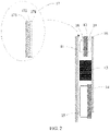
- FIG. 2 is a schematic diagram of a heat dissipation structure for an electronic device according to Embodiment 2 of this application.
- a heat dissipating layer 17 includes a heat equalizing layer 171.
- the heat equalizing layer 171 is in contact with a mainboard 12, a battery 13, and a speaker box 15.
- a first region of the heat equalizing layer 171 of the heat dissipating layer 17 may be in contact with a first shield cover 18 of the mainboard 12, and a second shield cover 19 of the mainboard 12 is in contact with a first region of a middle frame 16.
- a second region of the heat equalizing layer 171 is in contact with a surface of the battery 13.
- a third region of the heat equalizing layer 171 is in contact with a surface of the speaker box 15 that is distant from an antenna panel 14.
- the heat equalizing layer 171 may be formed by a thermally conductive material such as copper foil or graphite, and has a relatively high coefficient of planar thermal conductivity.
- the heat equalizing layer 171 can be configured to evenly dissipate heat absorbed from the mainboard 12, the battery 13, and the speaker box 15, to effectively avoid local heat dissipation of an electronic device.
- the coefficient of thermal conductivity of the heat equalizing layer 171 is greater than or equal to 250 W/(m ⁇ K).
- the heat dissipating layer 17 further includes a heat accumulating layer 172 and a heat insulation layer 173.
- the heat insulation layer 173 is in contact with a rear cover 11.
- the heat accumulating layer 172 is located between the heat insulation layer 173 and the heat equalizing layer 171.
- the heat accumulating layer 172 may be formed by a phase change material, and can absorb heat from the heat equalizing layer 171 by using a phase change, and store heat energy, to alleviate temperature rise of the rear cover 11 of the electronic device.
- the heat insulation layer 173 may be formed by a heat-insulation material, and can prevent heat from being directly transferred to the rear cover 11, to alleviate temperature rise of the rear cover 11 of the electronic device.
- the heat equalizing layer 171, the heat accumulating layer 172, and the heat insulation layer 173 may have different thicknesses.
- a thickness ratio of the heat equalizing layer 171, the heat accumulating layer 172, and the heat insulation layer 173 may be, for example, 2: 2.5: 3.
- the heat equalizing layer 171 may be in contact with a partial region of the surface of the speaker box 15 that is distant from the antenna panel 14. Coverage areas of the heat accumulating layer 172 and the heat insulation layer 173 may be greater than that of the heat equalizing layer.
- a specific heat capacity of the heat accumulating layer 172 is greater than or equal to 100 J/(g ⁇ K), and a coefficient of thermal conductivity of the heat insulation layer 173 is less than or equal to 0.5 W/(m ⁇ K).
- J is a heat unit Joule
- g is a mass unit gram
- K is a thermodynamic temperature unit Kelvin.
- the specific heat capacity of the heat accumulating layer 172 is greater than or equal to 100 J/(g ⁇ K)
- a heat storage capability of the heat accumulating layer 172 may be effectively ensured, to effectively alleviate temperature rise of the rear cover 11 of the electronic device.
- the coefficient of thermal conductivity of the heat insulation layer 173 is less than or equal to 0.5 W/(m ⁇ K)
- transfer of heat of the heat accumulating layer 172 to the rear cover 11 may also be effectively alleviated, to effectively alleviate temperature rise of the rear cover of the electronic device.
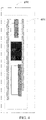
- FIG. 3 is a schematic diagram of another heat dissipation structure for an electronic device according to Embodiment 2 of this application.
- the middle frame 16 in a direction perpendicular to the heat dissipating layer 17, is further disposed with a first separating piece 161 and a second separating piece 162.
- the first separating piece 161 is configured to separate the mainboard 12 from the battery 13 along a longitudinal direction
- the second separating piece 162 is configured to separate the battery 13 from the antenna panel 14 along the longitudinal direction
- the longitudinal direction is a direction perpendicular to the heat dissipating layer 17.
- thermally conductive foam 20 is further disposed between the antenna panel 14 and the second separating piece 162.
- the heat dissipation structure for an electronic device may further include a front cover.
- the front cover may be a display screen of an electronic device.
- the front cover may be located on one side of the middle frame 16 that is distant from the rear cover 11.
- the thermally conductive foam 20 disposed between the antenna panel 14 and the second separating piece 162 may implement a heat conduction path sequentially including the battery 13, the second separating piece 162, the antenna panel 14, and the speaker box 15, to implement heat dissipation on the heat conduction path, and effectively avoid local heat generation of the electronic device.
- Embodiment 3 of this application further provides an electronic device.
- FIG. 4 is a schematic structural diagram of the electronic device according to Embodiment 3 of this application.
- the electronic device 40 may include a heat dissipation structure 41.
- the heat dissipation structure 41 may be any one of the heat dissipation structures in FIG. 1 to FIG. 3 .
- the electronic device provided in Embodiment 3 of this application may include any one of the foregoing heat dissipation structures for an electronic device. Therefore, heat dissipation of the mainboard and the battery inside the electronic device may be implemented, and heat dissipation of a region of the speaker box may also be implemented, to effectively avoid local heat generation of the electronic device, and implement equalized heat dissipation of the electronic device, thereby improving user experience.
Description
- Embodiments of this application relate to device dissipation technologies, and in particular, to a heat dissipation structure for an electronic device and an electronic device.
- With development of electronic communications technologies and use requirements of users on electronic devices, the electronic devices implement a growing quantity of functions, and the functions become increasingly perfect. Consequently, power consumption of the electronic device is increasingly high, that is, more heat is generated.
- A user may usually obtain a desired sound effect by increasing a volume of the electronic device. However, when the volume of the electronic device is increased, power of a speaker box of the electronic device is increased undoubtedly. Consequently, the speaker box generates more heat. In addition, heat of another element adjacent to the speaker box inside the electronic device is conducted to the speaker box. Consequently, the speaker box also generates more heat.
- Currently, the speaker box in the electronic device has a poor heat conduction effect. Consequently, heat dissipation of the speaker box is poor. In this case, when the speaker box generates heat, the heat cannot be effectively conducted for dissipation. Consequently, a partial region of the speaker box in the electronic device overheats.
-
US 2016/0109911 A1 discloses a solution to providing heat management and cooling to electronic devices. According to various embodiments, heat produced during the operation of the processing components in the computing device is absorbed by heat management features integrated within a supporting mid-frame. The heat management features include phase changing materials that allow the processing components to be kept at a isothermal state through changes in phase, thereby prolonging the duration of time in which the processing components can operate at high performance levels without the need to throttle the performance. -
CN 104601759 A discloses a cell phone heat radiation structure and a cell phone and relates to the technical field of the cell phones. The cell phone comprises a loudspeaker and receiver two-in-one front surface region, a main board region and an accessory region, wherein a camera region and an antenna region are arranged on the two sides of the loudspeaker and receiver two-in-one front surface region; the cell phone heat radiation structure comprises at least one heat radiation layer made of a heat radiation material; the heat radiation layer covers at least one part of the loudspeaker and receiver two-in-one front surface region and at least one part of the main board region. The invention further discloses the cell phone comprising the cell phone heat radiation structure. The problems that the temperature of existing loudspeaker and receiver two-in-one front surface region and main board region is too high are solved so that the loudspeaker and receiver two-in-one front surface region and the main board region are sufficiently radiated -
CN 2598039 A discloses an improved heat radiating structure for miniature trumpet inlayed thin material space. Principally, a heat radiating guide plate is arranged on rear metal base of internal inlay type miniature trumpet in thin material space of thin electronic products such as notebook, PDA and LCD, thus the heated metal base can transmit thermal energy to the heat radiating guide plate so as to enlarge heat radiation area of the miniature trumpet, prevent high temperature air concentrating in the miniature trumpet, strengthen heat radiation efficiency of the miniature trumpet, reduce temperature of voice coil inside the miniature trumpet, prevent the voice coil being burnt under high temperature, promote stability of outputted power, avoid hot air concentrating around the miniature trumpet aside shell of electronic product and prevent the shell of thin electronic product burning in high temperature. -
JP2009231907 A - Embodiments of this application provide a heat dissipation structure for an electronic device and an electronic device, to avoid local high temperature of the electronic device.
- An embodiment of this application provides a heat dissipation structure for an electronic device, including: a rear cover, a mainboard, a battery, an antenna panel, a speaker box, and a middle frame, where a heat dissipating layer is disposed on the rear cover, a first shield cover and a second shield cover are disposed on the mainboard, and the speaker box is disposed on a surface of the antenna panel;
- a first region of the heat dissipating layer is in contact with the first shield cover of the mainboard, and the second shield cover of the mainboard is in contact with a first region of the middle frame;
- a second region of the heat dissipating layer is in contact with a surface of the battery, and another surface of the battery that is distant from the heat dissipating layer is in contact with a second region of the middle frame; and
- a third region of the heat dissipating layer is in contact with a surface of the speaker box that is distant from the antenna panel, and another surface of the antenna panel that is distant from the speaker box is in contact with a third region of the middle frame.
- In the heat dissipation structure for an electronic device, because the heat dissipating layer disposed on the rear cover may be in contact with the mainboard and the battery, and may also be in contact with the speaker box, the heat dissipation structure for an electronic device implements heat dissipation of the mainboard and the battery, and may further implement heat dissipation of a region of the speaker box, to effectively avoid local high temperature, and implement equalized heat dissipation of the electronic device, thereby improving user experience.
- Optionally, the third region of the heat dissipating layer is in contact with a partial or entire region of the surface of the speaker box that is distant from the antenna panel.
- Optionally, the third region of the heat dissipating layer is in contact with the surface of the speaker box that is distant from the antenna panel in an adhesive manner, and an adhesive used in the adhesive manner is an adhesive for heat conduction.
- Optionally, the third region of the heat dissipating layer is in contact with the surface of the speaker box that is distant from the antenna panel in a welding manner.
- Because a material used in the adhesive manner or in the welding manner is a thermally conductive material, when the heat dissipating layer is in contact with the speaker box in the adhesive manner or in the welding manner, thermal conductivity between the heat dissipating layer and the speaker box may be improved, and heat transfer efficiency may be increased.
- Optionally, the first region of the heat dissipating layer may also be in contact with the first shield cover of the mainboard in an adhesive manner or in a welding manner, and the second shield cover of the mainboard may also be in contact with the first region of the middle frame in an adhesive manner or in a welding manner. An adhesive used in the adhesive manner may also be an adhesive for heat conduction, and a flux used in the welding manner is a thermally conductive flux.
- Because a material used in the adhesive manner or in the welding manner is a thermally conductive material, when the heat dissipating layer is in contact with the first shield cover in the adhesive manner or in the welding manner, thermal conductivity between the heat dissipating layer and the first shield cover may be improved, thereby improving thermal conductivity between the mainboard and the heat dissipating layer, and increasing heat transfer efficiency.
- Optionally, the second region of the heat dissipating layer may also be in contact with the battery in an adhesive manner or in a welding manner, and the another surface of the battery that is distant from the heat dissipating layer may also be in contact with the second region of middle frame in an adhesive manner or in a welding manner. An adhesive used in the adhesive manner may also be an adhesive for heat conduction, and a flux used in the welding manner is a thermally conductive flux.
- Because a material used in the adhesive manner or in the welding manner is a thermally conductive material, when the heat dissipating layer is in contact with the battery in the adhesive manner or in the welding manner, thermal conductivity between the heat dissipating layer and the battery may be improved, and heat transfer efficiency may be increased.
- Optionally, a material of the speaker box is a thermally conductive material, and the thermally conductive material includes any one of the following: thermally conductive plastic, ceramic, and metal.
- For the speaker box formed by a thermally conductive material, heat generated by an element inside the speaker box may be better conducted to a surface of the speaker box, for effective dissipation.
- Optionally, a dielectric constant of the thermally conductive material is less than or equal to 8, a loss angle of the thermally conductive material is less than or equal to 0.01, and a coefficient of thermal conductivity of the thermally conductive material is greater than or equal to 1 W/(m∗K).
- The dielectric constant of the thermally conductive material of the speaker box is less than or equal to 8, so that heat generated by an element inside the speaker box can be better conducted to a surface of the speaker box, to effectively avoid electrical interference from the element inside the speaker box. The coefficient of thermal conductivity of the thermally conductive material of the speaker box is greater than or equal to 1 W/(m∗K), so that heat conductivity between the element inside the speaker box and the speaker box is improved, and heat transfer efficiency is increased.
- Optionally, a charger is further disposed on the antenna panel.
- Heat generated by the charger in a charging process may be transferred to the speaker box by using the antenna panel, and then is dissipated by using the heat dissipating layer in contact with the speaker box. Heat dissipation of the region of the speaker box in a charging scenario may also be implemented, to avoid local high temperature of an electronic device, and improve user experience.
- Optionally, the heat dissipating layer includes a heat equalizing layer, and the heat equalizing layer is in contact with the mainboard, the battery, and the antenna panel.
- The heat equalizing layer can evenly dissipate heat absorbed from the mainboard, the battery, and the speaker box, to effectively avoid local heat dissipation of the electronic device.
- Optionally, a coefficient of thermal conductivity of the heat equalizing layer is greater than or equal to 250 W/(m∗K).
- Optionally, the heat dissipating layer further includes a heat accumulating layer and a heat insulation layer, the heat insulation layer is in contact with the rear cover, and the heat accumulating layer is located between the heat insulation layer and the heat equalizing layer.
- The heat accumulating layer can absorb heat from the heat equalizing layer by using a phase change, and stores heat energy, to alleviate temperature rise of the rear cover of the electronic device. The heat insulation layer can stop heat from being directly transferred to the rear cover, to alleviate temperature rise of the rear cover of the electronic device.
- Optionally, a specific heat capacity of the heat accumulating layer is greater than or equal to 100 J/(g∗K), and a coefficient of thermal conductivity of the heat insulation layer is less than or equal to 0.5 W/(m∗K).
- Optionally, in a direction perpendicular to the heat dissipating layer, the middle frame is further disposed with a first separating piece and a second separating piece, the first separating piece is configured to separate the mainboard from the battery along a longitudinal direction, the second separating piece is configured to separate the battery from the antenna panel along the longitudinal direction, and the longitudinal direction is a direction perpendicular to the heat dissipating layer.
- Optionally, thermally conductive foam is further disposed between the antenna panel and the second separating piece.
- The thermally conductive foam disposed between the antenna panel and the second separating piece may implement a heat conduction path sequentially including the battery, the second separating piece, the antenna panel, and the speaker box, to implement heat dissipation on the heat conduction path, and effectively avoid local heat generation of the electronic device.
- An embodiment of this application further provides an electronic device, including the heat dissipation structure according to any one of the foregoing descriptions.
- The heat dissipation structure for an electronic device and the electronic device are provided in the embodiments of this application. The heat dissipation structure for an electronic device may include the rear cover, the mainboard, the battery, the antenna panel, the speaker box, and the middle frame. The heat dissipating layer is disposed on the rear cover. The first shield cover and the second shield cover are disposed on the mainboard. The speaker box is disposed on the surface of the antenna panel. The first region of the heat dissipating layer is in contact with the first shield cover of the mainboard, and the second shield cover of the mainboard is in contact with the first region of the middle frame. The second region of the heat dissipating layer is in contact with the surface of the battery, and the another surface of the battery that is distant from the heat dissipating layer is in contact with the second region of the middle frame. The third region of the heat dissipating layer is in contact with the surface of the speaker box that is distant from the antenna panel, and the another surface of the antenna panel that is distant from the speaker box is in contact with the third region of the middle frame. In the heat dissipation structure for an electronic device, because the heat dissipating layer disposed on the rear cover may be in contact with the mainboard and the battery, and may also be in contact with the speaker box, the heat dissipation structure for an electronic device implements heat dissipation of the mainboard and the battery, and may further implement heat dissipation of the region of the speaker box, to effectively avoid local high temperature, and implement equalized heat dissipation of the electronic device, thereby improving user experience.
- To describe technical solutions in embodiments of this application or in the prior art more clearly, the following briefly describes the accompanying drawings required for describing the embodiments or the prior art. Apparently, the accompanying drawings in the following description show some embodiments of this application, and persons of ordinary skill in the art may still derive other drawings from these accompanying drawings without creative efforts.
-
FIG. 1 is a schematic diagram of a heat dissipation structure for an electronic device according to Embodiment 1 of this application; -
FIG. 2 is a schematic diagram of a heat dissipation structure for an electronic device according to Embodiment 2 of this application; -
FIG. 3 is a schematic diagram of another heat dissipation structure for an electronic device according to Embodiment 2 of this application; and -
FIG. 4 is a schematic structural diagram of an electronic device according to Embodiment 3 of this application. - Reference numerals:
- 11: Rear cover;
- 12: Mainboard;
- 13: Battery;
- 14: Antenna panel;
- 15: Speaker box;
- 16: Middle frame;
- 161: First separating piece;
- 162: Second separating piece;
- 17: Heat dissipating layer;
- 171: Heat equalizing layer;
- 172: Heat accumulating layer;
- 173: Insulation layer;
- 18: First shield cover;
- 19: Second shield cover;
- 20: Thermally conductive foam;
- 40: Electronic device;
- 41: Heat dissipation structure.
- To make the objectives, technical solutions, and advantages of the embodiments of this application clearer, the following clearly and completely describes the technical solutions in the embodiments of this application with reference to the accompanying drawings in the embodiments of this application. Apparently, the described embodiments are some but not all of the embodiments of this application. All other embodiments obtained by persons of ordinary skill in the art based on the embodiments of this application without creative efforts shall fall within the protection scope of this application.
- Embodiment 1 of this application provides a heat dissipation structure for an electronic device. The heat dissipation structure may be located in an electronic device. For example, the electronic device may be an electronic device such as a mobile phone, a notebook computer, or a tablet computer.
FIG. 1 is a schematic diagram of the heat dissipation structure for an electronic device according to Embodiment 1 of this application. As shown inFIG. 1 , the heat dissipation structure for an electronic device may include: arear cover 11, amainboard 12, abattery 13, anantenna panel 14, aspeaker box 15, and amiddle frame 16. Aheat dissipating layer 17 is disposed on therear cover 11. Afirst shield cover 18 and asecond shield cover 19 are disposed on themainboard 12. Thespeaker box 15 is disposed on a surface of theantenna panel 14. - A first region of the
heat dissipating layer 17 is in contact with thefirst shield cover 18 of themainboard 12, and thesecond shield cover 19 of themainboard 12 is in contact with a first region of themiddle frame 16. - A second region of the
heat dissipating layer 17 is in contact with a surface of thebattery 13, and the other surface of thebattery 13 that is distant from theheat dissipating layer 17 is in contact with a second region of themiddle frame 16. - A third region of the
heat dissipating layer 17 is in contact with a surface of thespeaker box 15 that is distant from theantenna panel 14, and the other surface of theantenna panel 14 that is distant from thespeaker box 15 is in contact with a third region of themiddle frame 16. - Specifically, the
mainboard 12 and theantenna panel 14 each may be a printed circuit board (Printed Circuit Board, PCB for short). An element such as a processor may be integrated on themainboard 12, and an antenna element such as wiring of an antenna array may be integrated on theantenna panel 14. For example, the antenna element may include at least one antenna of a mobile communications antenna, a Wireless Fidelity (Wireless-Fidelity, Wi-Fi for short) antenna, a Global Positioning System (Global Positioning System, GPS for short) antenna, a Bluetooth (Bluetooth) antenna, a Near Field Communication (Near Field Communication, NFC for short) antenna, a wireless charging (Wireless Charge) antenna, and the like. The mobile communications antenna may be at least one of a 2nd generation (2nd Generation, 2G for short) communications antenna, a 3rd generation (3rd Generation, 3G for short) communications antenna, a 4th generation (4th Generation, 4G for short) communications antenna, a 5th generation (5th Generation, 5G for short) communications antenna, and an antenna using a subsequently evolved communication technology. For example, the antenna element may be in a range from 450 MHz to 5 GHz. Usually, themainboard 12 may also be referred to as a large board, and the correspondingantenna panel 14 may be referred to as a small board. - The
mainboard 12 is disposed with a plurality of shield covers. Interference from a neighboring element to an element on themainboard 12 is isolated by using a shield cover. That is, the shield cover is configured to shield and protect electrical characteristics of the element on themainboard 12. Thefirst shield cover 18 prefers to a shield cover that is in the plurality of shield covers and that is in contact with theheat dissipating layer 17, and thesecond shield cover 19 refers to a shield cover that is in the plurality of shield covers and that is in contact with themiddle frame 16. That is, thefirst shield cover 18 and thesecond shield cover 19 each refer to shield covers of one class, and each includes at least one shield cover. It should be noted thatFIG. 1 is described by using only a case in which thefirst shield cover 18 and thesecond shield cover 19 each include one shield cover. This application is not limited thereto. - The
speaker box 15 may include a sound element such as a speaker (Speaker) and a receiver (Receiver). The speaker and the receiver are disposed on theantenna panel 14. Theheat dissipating layer 17 may be a thermally conductive layer formed by a thermally conductive material whose coefficient of thermal conductivity is greater than a preset coefficient, or may be a composite thermally conductive layer formed by a thermally conductive material and another material. This application is not limited thereto. - The first region of the
heat dissipating layer 17 is in contact with thefirst shield cover 18 of themainboard 12, so that heat of themainboard 12 is transferred to theheat dissipating layer 17 by using thefirst shield cover 18, to dissipate heat of a region of themainboard 12. Thesecond shield cover 19 of themainboard 12 is in contact with the first region of themiddle frame 16, so that themainboard 12 is secured to themiddle frame 16, to enable themainboard 12 to be stable in the electronic device, and effectively ensure performance of the element on themainboard 12. - The second region of the
heat dissipating layer 17 is in contact with the surface of thebattery 13, so that heat of thebattery 13 is transferred to theheat dissipating layer 17, to implement heat dissipation of a region of thebattery 13. The other surface of thebattery 13 that is distant from theheat dissipating layer 17 is also in contact with the second region of themiddle frame 16, so that thebattery 13 is secured to themiddle frame 16, to enable thebattery 13 to be stable in the electronic device. - The third region of the
heat dissipating layer 17 is in contact with the surface of thespeaker box 15 that is distant from theantenna panel 14. A thermal correlation between theheat dissipating layer 17 and thespeaker box 15 is actually established, so that heat of thespeaker box 15 is transferred to theheat dissipating layer 17, to implement heat dissipation of a region of thespeaker box 15. The other surface of theantenna panel 14 that is distant from thespeaker box 15 is in contact with the third region of themiddle frame 16, and theantenna panel 14 may be secured to themiddle frame 16, so that theantenna panel 14 is stable in the electronic device. It should be noted that the heat of thespeaker box 15 includes heat generated by a heat emitting element inside thespeaker box 15, and further includes heat generated by a part adjacent to thespeaker box 15, for example, theantenna panel 14. - The heat dissipation structure for an electronic device provided in Embodiment 1 of this application includes the rear cover, the mainboard, the battery, the antenna panel, the speaker box, and the middle frame. The heat dissipating layer is disposed on the rear cover. The first shield cover and the second shield cover are disposed on the mainboard. The speaker box is disposed on the surface of the antenna panel. The first region of the heat dissipating layer is in contact with the first shield cover of the mainboard, and the second shield cover of the mainboard is in contact with the first region of the middle frame. The second region of the heat dissipating layer is in contact with the surface of the battery, and the other surface of the battery that is distant from the heat dissipating layer is in contact with the second region of the middle frame. The third region of the heat dissipating layer is in contact with the surface of the speaker box that is distant from the antenna panel, and the other surface of the antenna panel that is distant from the speaker box is in contact with the third region of the middle frame. In the heat dissipation structure for an electronic device, because the heat dissipating layer disposed on the rear cover may be in contact with the mainboard and the battery, and may also be in contact with the speaker box, the heat dissipation structure for an electronic device implements heat dissipation of the mainboard and the battery, and may further implement heat dissipation of the region of the speaker box, to effectively avoid local high temperature in scenarios such as a game, a video, and music, and implement equalized heat dissipation of the electronic device, thereby improving user experience.
- The third region of the
heat dissipating layer 17 is in contact with a partial or entire region of the surface of thespeaker box 15 that is distant from theantenna panel 14. - Optionally, the third region of the
heat dissipating layer 17 may be in contact with the surface of thespeaker box 15 that is distant from theantenna panel 14 in an adhesive manner or in a welding manner. An adhesive used in the adhesive manner is an adhesive for heat conduction, and a flux used in the welding manner is a thermally conductive flux. - The other surface of the
antenna panel 14 that is distant from thespeaker box 15 may be in contact with the third region of themiddle frame 16 by using a screw. For example, the screw may be a thermally conductive screw. - Specifically, because the material used in the adhesive manner or in the welding manner is a thermally conductive material, when the
heat dissipating layer 17 is in contact with thespeaker box 15 in the adhesive manner or in the welding manner, thermal conductivity between theheat dissipating layer 17 and thespeaker box 15 may be improved, and heat transfer efficiency may be increased. - Optionally, the first region of the
heat dissipating layer 17 may also be in contact with thefirst shield cover 18 of themainboard 12 in an adhesive manner or in a welding manner, and thesecond shield cover 19 of themainboard 12 may also be in contact with the first region of themiddle frame 16 in an adhesive manner or in a welding manner. An adhesive used in the adhesive manner may also be an adhesive for heat conduction, and a flux used in the welding manner is a thermally conductive flux. - Specifically, because the material used in the adhesive manner or in the welding manner is a thermally conductive material, when the
heat dissipating layer 17 is in contact with thefirst shield cover 18 in the adhesive manner or in the welding manner, thermal conductivity between theheat dissipating layer 17 and thefirst shield cover 18 may be improved, thereby improving thermal conductivity between themainboard 12 and the heat dissipating layer, and increasing heat transfer efficiency. - Optionally, the second region of the
heat dissipating layer 17 may also be in contact with thebattery 13 in an adhesive manner or in a welding manner, and the other surface of thebattery 13 that is distant from theheat dissipating layer 17 may also be in contact with the second region ofmiddle frame 16 in an adhesive manner or in a welding manner. An adhesive used in the adhesive manner may also be an adhesive for heat conduction, and a flux used in the welding manner is a thermally conductive flux. - Specifically, because the material used in the adhesive manner or in the welding manner is a thermally conductive material, when the
heat dissipating layer 17 is in contact with thebattery 13 in the adhesive manner or in the welding manner, thermal conductivity between theheat dissipating layer 17 and thebattery 13 may be improved, and heat transfer efficiency may be increased. - Optionally, a material of the
speaker box 15 is a thermally conductive material, and the thermally conductive material includes any one of the following: thermally conductive plastic, ceramic, metal, and the like. - Specifically, a material of the
speaker box 15 is set to a thermally conductive material, so that heat generated by an element inside thespeaker box 15 may be better conducted to a surface of thespeaker box 15, for effective dissipation. It should be noted that the material of thespeaker box 15 may alternatively be another thermally conductive material. The thermally conductive plastic, ceramic, and metal are only examples for illustration. This application is not limited thereto. - Optionally, a dielectric constant of the thermally conductive material is less than or equal to 8, a loss angle of the thermally conductive material is less than or equal to 0.01, and a coefficient of thermal conduction of the thermally conductive material is greater than or equal to 1 W/(m∗K). W is a heat unit watt, m is a unit meter, and K is a thermodynamic temperature unit Kelvin.
- Specifically, the dielectric constant of the thermally conductive material of the
speaker box 15 is less than or equal to 8, so that heat generated by the element inside thespeaker box 15 may be better conducted to the surface of thespeaker box 15, to effectively avoid electrical interference from the element inside thespeaker box 15. The coefficient of thermal conductivity of the thermally conductive material of thespeaker box 15 is greater than or equal to 1 W/(m∗K), so that heat conductivity between the element inside thespeaker box 15 and thespeaker box 15 is improved, and heat transfer efficiency is increased. - Optionally, the
antenna panel 14 is further disposed with a charger. The charger may be located inside thespeaker box 15. - Specifically, heat generated by the charger in a charging process may be transferred to the
speaker box 15 by using theantenna panel 14, and then is dissipated by using theheat dissipating layer 17 in contact with thespeaker box 15. Heat dissipation of the region of the speaker box in a charging scenario may also be implemented, to avoid local high temperature of the electronic device, and improve user experience. -
FIG. 2 is a schematic diagram of a heat dissipation structure for an electronic device according to Embodiment 2 of this application. As shown inFIG. 2 , in the foregoing heat dissipation structure for an electronic device, aheat dissipating layer 17 includes aheat equalizing layer 171. Theheat equalizing layer 171 is in contact with amainboard 12, abattery 13, and aspeaker box 15. - Specifically, a first region of the
heat equalizing layer 171 of theheat dissipating layer 17 may be in contact with afirst shield cover 18 of themainboard 12, and asecond shield cover 19 of themainboard 12 is in contact with a first region of amiddle frame 16. A second region of theheat equalizing layer 171 is in contact with a surface of thebattery 13. A third region of theheat equalizing layer 171 is in contact with a surface of thespeaker box 15 that is distant from anantenna panel 14. - The
heat equalizing layer 171 may be formed by a thermally conductive material such as copper foil or graphite, and has a relatively high coefficient of planar thermal conductivity. Theheat equalizing layer 171 can be configured to evenly dissipate heat absorbed from themainboard 12, thebattery 13, and thespeaker box 15, to effectively avoid local heat dissipation of an electronic device. - Optionally, the coefficient of thermal conductivity of the
heat equalizing layer 171 is greater than or equal to 250 W/(m∗K). - Optionally, the
heat dissipating layer 17 further includes aheat accumulating layer 172 and aheat insulation layer 173. Theheat insulation layer 173 is in contact with arear cover 11. Theheat accumulating layer 172 is located between theheat insulation layer 173 and theheat equalizing layer 171. - Specifically, the
heat accumulating layer 172 may be formed by a phase change material, and can absorb heat from theheat equalizing layer 171 by using a phase change, and store heat energy, to alleviate temperature rise of therear cover 11 of the electronic device. Theheat insulation layer 173 may be formed by a heat-insulation material, and can prevent heat from being directly transferred to therear cover 11, to alleviate temperature rise of therear cover 11 of the electronic device. Theheat equalizing layer 171, theheat accumulating layer 172, and theheat insulation layer 173 may have different thicknesses. A thickness ratio of theheat equalizing layer 171, theheat accumulating layer 172, and theheat insulation layer 173 may be, for example, 2: 2.5: 3. - To ensure electrical performance of an antenna element on the
antenna panel 14, theheat equalizing layer 171 may be in contact with a partial region of the surface of thespeaker box 15 that is distant from theantenna panel 14. Coverage areas of theheat accumulating layer 172 and theheat insulation layer 173 may be greater than that of the heat equalizing layer. - Optionally, a specific heat capacity of the
heat accumulating layer 172 is greater than or equal to 100 J/(g∗K), and a coefficient of thermal conductivity of theheat insulation layer 173 is less than or equal to 0.5 W/(m∗K). J is a heat unit Joule, g is a mass unit gram, and K is a thermodynamic temperature unit Kelvin. - When the specific heat capacity of the
heat accumulating layer 172 is greater than or equal to 100 J/(g∗K), a heat storage capability of theheat accumulating layer 172 may be effectively ensured, to effectively alleviate temperature rise of therear cover 11 of the electronic device. In addition, when the coefficient of thermal conductivity of theheat insulation layer 173 is less than or equal to 0.5 W/(m∗K), transfer of heat of theheat accumulating layer 172 to therear cover 11 may also be effectively alleviated, to effectively alleviate temperature rise of the rear cover of the electronic device. -
FIG. 3 is a schematic diagram of another heat dissipation structure for an electronic device according to Embodiment 2 of this application. As shown inFIG. 3 , in any one of the foregoing heat dissipation structures for an electronic device, in a direction perpendicular to theheat dissipating layer 17, themiddle frame 16 is further disposed with afirst separating piece 161 and asecond separating piece 162. Thefirst separating piece 161 is configured to separate themainboard 12 from thebattery 13 along a longitudinal direction, thesecond separating piece 162 is configured to separate thebattery 13 from theantenna panel 14 along the longitudinal direction, and the longitudinal direction is a direction perpendicular to theheat dissipating layer 17. - Optionally, thermally
conductive foam 20 is further disposed between theantenna panel 14 and thesecond separating piece 162. - Optionally, the heat dissipation structure for an electronic device may further include a front cover. For example, the front cover may be a display screen of an electronic device. The front cover may be located on one side of the
middle frame 16 that is distant from therear cover 11. - The thermally
conductive foam 20 disposed between theantenna panel 14 and thesecond separating piece 162 may implement a heat conduction path sequentially including thebattery 13, thesecond separating piece 162, theantenna panel 14, and thespeaker box 15, to implement heat dissipation on the heat conduction path, and effectively avoid local heat generation of the electronic device. - Embodiment 3 of this application further provides an electronic device.
FIG. 4 is a schematic structural diagram of the electronic device according to Embodiment 3 of this application. As shown inFIG. 4 , the electronic device 40 may include a heat dissipation structure 41. The heat dissipation structure 41 may be any one of the heat dissipation structures inFIG. 1 to FIG. 3 . - The electronic device provided in Embodiment 3 of this application may include any one of the foregoing heat dissipation structures for an electronic device. Therefore, heat dissipation of the mainboard and the battery inside the electronic device may be implemented, and heat dissipation of a region of the speaker box may also be implemented, to effectively avoid local heat generation of the electronic device, and implement equalized heat dissipation of the electronic device, thereby improving user experience.
- Finally, it should be noted that: The foregoing embodiments are merely intended for describing the technical solutions of this application defined by claims.
Claims (14)
- A heat dissipation structure for an electronic device, comprising: a rear cover (11), a mainboard (12), a battery (13), an antenna panel (14), a speaker box (15), and a middle frame (16), wherein a heat dissipating layer (17) is disposed on the rear cover (11), a first shield cover (18) and a second shield cover (19) are disposed on the mainboard (12), and the speaker box (15) is disposed on a surface of the antenna panel (14);a first region of the heat dissipating layer (17) is in contact with the first shield cover (18) of the mainboard (12), and the second shield cover (19) of the mainboard (12) is in contact with a first region of the middle frame (16);a second region of the heat dissipating layer (17) is in contact with a surface of the battery (13), and another surface of the battery (13) that is distant from the heat dissipating layer (17) is in contact with a second region of the middle frame (16); anda third region of the heat dissipating layer (17) is in contact with a surface of the speaker box (15) that is distant from the antenna panel (14), and another surface of the antenna panel (14) that is distant from the speaker box (15) is in contact with a third region of the middle frame (16).
- The heat dissipation structure according to claim 1, wherein the third region of the heat dissipating layer (17) is in contact with a partial or entire region of the surface of the speaker box (15) that is distant from the antenna panel (14).
- The heat dissipation structure according to claim 1 or 2, wherein the third region of the heat dissipating layer (17) is in contact with the surface of the speaker box (15) that is distant from the antenna panel (14) in an adhesive manner, and an adhesive used in the adhesive manner is an adhesive for heat conduction.
- The heat dissipation structure according to claim 1 or 2, wherein the third region of the heat dissipating layer (17) is in contact with the surface of the speaker box (15) that is distant from the antenna panel (14) in a welding manner.
- The heat dissipation structure according to any one of claims 1 to 4, wherein a material of the speaker box (15) is a thermally conductive material, and the thermally conductive material (20) comprises any one of the following: thermally conductive plastic, ceramic, and metal.
- The heat dissipation structure according to claim 5, wherein a dielectric constant of the thermally conductive material (20) is less than or equal to 8, a loss angle of the thermally conductive material (20) is less than or equal to 0.01, and a coefficient of thermal conductivity of the thermally conductive material (20) is greater than or equal to 1 W/(m∗K).
- The heat dissipation structure according to any one of claims 1 to 6, wherein a charger is further disposed on the antenna panel (14).
- The heat dissipation structure according to any one of claims 1 to 7, wherein the heat dissipating layer (17) comprises a heat equalizing layer, and the heat equalizing layer is in contact with the mainboard (12), the battery (13), and the antenna panel (14).
- The heat dissipation structure according to claim 8, wherein a coefficient of thermal conductivity of the heat equalizing layer is greater than or equal to 250 W/(m∗K).
- The heat dissipation structure according to claim 8, wherein the heat dissipating layer (17) further comprises a heat accumulating layer (172) and a heat insulation layer (173), the heat insulation layer (173) is in contact with the rear cover (11), and the heat accumulating layer (17) is located between the heat insulation layer (173) and the heat equalizing layer (171).
- The heat dissipation structure according to claim 10, wherein a specific heat capacity of the heat accumulating layer (172) is greater than or equal to 100 J/(g∗K), and a coefficient of thermal conductivity of the heat insulation layer (173) is less than or equal to 0.5 W/(m∗K).
- The heat dissipation structure according to any one of claims 1 to 11, wherein in a direction perpendicular to the heat dissipating layer (17), the middle frame (16) is further disposed with a first separating piece (161) and a second separating piece (162), the first separating piece (161) is configured to separate the mainboard (12) from the battery along a longitudinal direction, the second separating piece (162) is configured to separate the battery (13) from the antenna panel (14) along the longitudinal direction, and the longitudinal direction is a direction perpendicular to the heat dissipating layer (17).
- The heat dissipation structure according to claim 12, wherein thermally conductive foam is further disposed between the antenna panel (14) and the second separating piece (162).
- An electronic device, comprising the heat dissipation structure according to any one of claims 1 to 13.
Priority Applications (1)
| Application Number | Priority Date | Filing Date | Title |
|---|---|---|---|
| EP22159744.6A EP4099809A1 (en) | 2016-09-28 | 2017-09-27 | Heat dissipation structure for electronic device and electronic device |
Applications Claiming Priority (2)
| Application Number | Priority Date | Filing Date | Title |
|---|---|---|---|
| CN201621093416.3U CN206472427U (en) | 2016-09-28 | 2016-09-28 | Radiating structure for electronic equipment and electronic equipment |
| PCT/CN2017/103830 WO2018059464A1 (en) | 2016-09-28 | 2017-09-27 | Heat dissipation structure for electronic device, and electronic device |
Related Child Applications (2)
| Application Number | Title | Priority Date | Filing Date |
|---|---|---|---|
| EP22159744.6A Division EP4099809A1 (en) | 2016-09-28 | 2017-09-27 | Heat dissipation structure for electronic device and electronic device |
| EP22159744.6A Division-Into EP4099809A1 (en) | 2016-09-28 | 2017-09-27 | Heat dissipation structure for electronic device and electronic device |
Publications (3)
| Publication Number | Publication Date |
|---|---|
| EP3512318A1 EP3512318A1 (en) | 2019-07-17 |
| EP3512318A4 EP3512318A4 (en) | 2019-11-27 |
| EP3512318B1 true EP3512318B1 (en) | 2022-04-06 |
Family
ID=59709695
Family Applications (2)
| Application Number | Title | Priority Date | Filing Date |
|---|---|---|---|
| EP17854914.3A Active EP3512318B1 (en) | 2016-09-28 | 2017-09-27 | Heat dissipation structure for electronic device, and electronic device |
| EP22159744.6A Pending EP4099809A1 (en) | 2016-09-28 | 2017-09-27 | Heat dissipation structure for electronic device and electronic device |
Family Applications After (1)
| Application Number | Title | Priority Date | Filing Date |
|---|---|---|---|
| EP22159744.6A Pending EP4099809A1 (en) | 2016-09-28 | 2017-09-27 | Heat dissipation structure for electronic device and electronic device |
Country Status (5)
| Country | Link |
|---|---|
| US (2) | US10729036B2 (en) |
| EP (2) | EP3512318B1 (en) |
| CN (1) | CN206472427U (en) |
| ES (1) | ES2913260T3 (en) |
| WO (1) | WO2018059464A1 (en) |
Cited By (1)
| Publication number | Priority date | Publication date | Assignee | Title |
|---|---|---|---|---|
| TWI799339B (en) * | 2022-08-22 | 2023-04-11 | 華碩電腦股份有限公司 | Handheld electronic device |
Families Citing this family (21)
| Publication number | Priority date | Publication date | Assignee | Title |
|---|---|---|---|---|
| CN206472427U (en) | 2016-09-28 | 2017-09-05 | 华为技术有限公司 | Radiating structure for electronic equipment and electronic equipment |
| US10819921B2 (en) | 2017-05-25 | 2020-10-27 | Google Llc | Camera assembly having a single-piece cover element |
| US10972685B2 (en) | 2017-05-25 | 2021-04-06 | Google Llc | Video camera assembly having an IR reflector |
| US10352496B2 (en) | 2017-05-25 | 2019-07-16 | Google Llc | Stand assembly for an electronic device providing multiple degrees of freedom and built-in cables |
| CN108566764B (en) * | 2018-04-16 | 2020-05-22 | 广东小天才科技有限公司 | Intelligent electronic equipment |
| CN112673717A (en) * | 2018-09-14 | 2021-04-16 | 深圳市柔宇科技股份有限公司 | Foldable electronic device |
| KR102567451B1 (en) * | 2018-11-22 | 2023-08-16 | 삼성전자주식회사 | Electronic device including the antenna module |
| CN111641025B (en) * | 2019-03-01 | 2022-08-09 | Oppo广东移动通信有限公司 | Antenna module and electronic equipment |
| CN110198624B (en) * | 2019-05-29 | 2021-07-13 | 浙江康廷电子科技有限公司 | Heat-insulation heat-conduction wave-absorbing material and preparation method thereof |
| CN110600834A (en) * | 2019-09-02 | 2019-12-20 | Oppo(重庆)智能科技有限公司 | Battery cover of electronic equipment and electronic equipment |
| CN110621141A (en) * | 2019-09-23 | 2019-12-27 | Oppo广东移动通信有限公司 | Composite film and electronic device |
| CN112804851A (en) * | 2019-10-28 | 2021-05-14 | 华为终端有限公司 | Electronic equipment |
| CN111243202A (en) * | 2020-01-15 | 2020-06-05 | 王芳 | Multifunctional financial electronic device |
| CN112261186B (en) * | 2020-10-23 | 2022-08-05 | 维沃移动通信有限公司 | Electronic device |
| US11592883B2 (en) * | 2021-07-30 | 2023-02-28 | Dell Products L.P. | Information handling system thermal management for dense structures |
| CN116646707A (en) * | 2021-09-07 | 2023-08-25 | 荣耀终端有限公司 | Electronic equipment |
| CN113939121B (en) * | 2021-10-08 | 2023-07-18 | 展讯通信(深圳)有限公司 | Electronic equipment shell with heat dissipation function and heat dissipation control method |
| CN116033699A (en) * | 2021-10-25 | 2023-04-28 | 群创光电股份有限公司 | Electronic device |
| CN113949171B (en) * | 2021-11-17 | 2023-06-30 | 重庆前卫无线电能传输研究院有限公司 | Rail type wireless charging pickup and forming method thereof |
| US20240074113A1 (en) * | 2022-08-30 | 2024-02-29 | roVa Corporation | Aerogel heat extraction apparatus for data centers and energy storage systems |
| US20240068755A1 (en) * | 2022-08-30 | 2024-02-29 | roVa Corporation | Aerogel heat extraction sheets, cables, and apparatus |
Family Cites Families (34)
| Publication number | Priority date | Publication date | Assignee | Title |
|---|---|---|---|---|
| US4768286A (en) * | 1986-10-01 | 1988-09-06 | Eastman Christensen Co. | Printed circuit packaging for high vibration and temperature environments |
| US5060114A (en) * | 1990-06-06 | 1991-10-22 | Zenith Electronics Corporation | Conformable pad with thermally conductive additive for heat dissipation |
| US5402313A (en) * | 1993-05-21 | 1995-03-28 | Cummins Engine Company, Inc. | Electronic component heat sink attachment using a canted coil spring |
| US5396403A (en) * | 1993-07-06 | 1995-03-07 | Hewlett-Packard Company | Heat sink assembly with thermally-conductive plate for a plurality of integrated circuits on a substrate |
| US5956576A (en) * | 1996-09-13 | 1999-09-21 | International Business Machines Corporation | Enhanced protection of semiconductors with dual surface seal |
| US6180436B1 (en) * | 1998-05-04 | 2001-01-30 | Delco Electronics Corporation | Method for removing heat from a flip chip semiconductor device |
| BRPI0100051B1 (en) * | 2001-01-11 | 2016-11-29 | Brasil Compressores Sa | electronic device enclosure |
| US6965071B2 (en) * | 2001-05-10 | 2005-11-15 | Parker-Hannifin Corporation | Thermal-sprayed metallic conformal coatings used as heat spreaders |
| CN2598039Y (en) * | 2002-12-06 | 2004-01-07 | 李秉彧 | Inserted thin material space improved radiating structure for small horn |
| US7031162B2 (en) * | 2003-09-26 | 2006-04-18 | International Business Machines Corporation | Method and structure for cooling a dual chip module with one high power chip |
| KR100608730B1 (en) * | 2003-12-20 | 2006-08-04 | 엘지전자 주식회사 | Case for mobile terminal with function of heat radiation |
| JP5028650B2 (en) * | 2008-03-19 | 2012-09-19 | 富士通モバイルコミュニケーションズ株式会社 | Mobile phone equipment |
| US8587945B1 (en) * | 2012-07-27 | 2013-11-19 | Outlast Technologies Llc | Systems structures and materials for electronic device cooling |
| CN203040086U (en) | 2012-12-07 | 2013-07-03 | 中兴通讯股份有限公司 | Terminal heat radiation apparatus |
| CN105162904A (en) | 2012-12-10 | 2015-12-16 | 华为终端有限公司 | Mobile terminal |
| CN203151921U (en) | 2012-12-21 | 2013-08-21 | 深圳市捷视飞通科技有限公司 | Heat conducting device of handheld equipment |
| CN203722986U (en) | 2014-01-03 | 2014-07-16 | 中兴通讯股份有限公司 | Mobile terminal |
| JP6311111B2 (en) | 2014-01-29 | 2018-04-18 | パナソニックIpマネジメント株式会社 | Heat dissipation structure |
| KR102184621B1 (en) * | 2014-02-21 | 2020-11-30 | 삼성전자주식회사 | Mobile communication terminal with radiat-heat sheet |
| TWI510174B (en) * | 2014-05-01 | 2015-11-21 | Taiwan Green Point Entpr Co | Heat-dissipation unit for electronic device and an electronic device comprising the heat-dissipation unit |
| CN203896662U (en) | 2014-06-27 | 2014-10-22 | 广东欧珀移动通信有限公司 | Mobile terminal composite type heat radiating structure and mobile phone |
| CN105472941A (en) | 2014-09-30 | 2016-04-06 | 联发科技(新加坡)私人有限公司 | Mobile phone and manufacturing method thereof |
| US9836100B2 (en) | 2014-10-15 | 2017-12-05 | Futurewei Technologies, Inc. | Support frame with integrated phase change material for thermal management |
| CN104601759B (en) * | 2015-02-02 | 2018-03-23 | 广东欧珀移动通信有限公司 | A kind of mobile phone radiator structure and mobile phone |
| US9901009B2 (en) * | 2015-03-10 | 2018-02-20 | Toshiba Memory Corporation | Semiconductor memory device |
| KR102418473B1 (en) * | 2015-04-08 | 2022-07-08 | 삼성전자주식회사 | Noise shielding device with heat sink structure and electronic device having it |
| CN105072868B (en) | 2015-07-14 | 2018-04-27 | 广东欧珀移动通信有限公司 | Mobile terminal and the method to mobile terminal heat dissipation |
| US10120423B1 (en) * | 2015-09-09 | 2018-11-06 | Amazon Technologies, Inc. | Unibody thermal enclosure |
| CN105246314B (en) | 2015-10-14 | 2018-09-04 | 小米科技有限责任公司 | Shielding case, pcb board and terminal device |
| CN105763682A (en) | 2016-04-06 | 2016-07-13 | 努比亚技术有限公司 | Mobile terminal |
| CN105744811B (en) | 2016-04-29 | 2018-12-11 | 广东欧珀移动通信有限公司 | Shell and mobile terminal |
| CN108601292B (en) | 2016-04-29 | 2020-07-21 | Oppo广东移动通信有限公司 | Rear shell and mobile terminal |
| CN206472427U (en) * | 2016-09-28 | 2017-09-05 | 华为技术有限公司 | Radiating structure for electronic equipment and electronic equipment |
| CN107547997B (en) | 2017-10-13 | 2020-06-02 | Oppo广东移动通信有限公司 | Circuit board assembly and electronic equipment |
-
2016
- 2016-09-28 CN CN201621093416.3U patent/CN206472427U/en active Active
-
2017
- 2017-09-27 EP EP17854914.3A patent/EP3512318B1/en active Active
- 2017-09-27 US US16/337,052 patent/US10729036B2/en active Active
- 2017-09-27 WO PCT/CN2017/103830 patent/WO2018059464A1/en unknown
- 2017-09-27 ES ES17854914T patent/ES2913260T3/en active Active
- 2017-09-27 EP EP22159744.6A patent/EP4099809A1/en active Pending
-
2020
- 2020-07-10 US US16/925,433 patent/US11122710B2/en active Active
Cited By (1)
| Publication number | Priority date | Publication date | Assignee | Title |
|---|---|---|---|---|
| TWI799339B (en) * | 2022-08-22 | 2023-04-11 | 華碩電腦股份有限公司 | Handheld electronic device |
Also Published As
| Publication number | Publication date |
|---|---|
| EP3512318A4 (en) | 2019-11-27 |
| US20190394905A1 (en) | 2019-12-26 |
| EP4099809A1 (en) | 2022-12-07 |
| CN206472427U (en) | 2017-09-05 |
| US10729036B2 (en) | 2020-07-28 |
| EP3512318A1 (en) | 2019-07-17 |
| ES2913260T3 (en) | 2022-06-01 |
| US11122710B2 (en) | 2021-09-14 |
| WO2018059464A1 (en) | 2018-04-05 |
| US20200344915A1 (en) | 2020-10-29 |
Similar Documents
| Publication | Publication Date | Title |
|---|---|---|
| EP3512318B1 (en) | Heat dissipation structure for electronic device, and electronic device | |
| EP3893327A1 (en) | Millimeter wave module and electronic device | |
| US9268376B2 (en) | Mobile computing device dock station with headset jack heat pipe interface | |
| US7286360B2 (en) | Heat radiating system and method for a mobile communication terminal | |
| US11202363B2 (en) | Heat transfer member and electronic device including the same | |
| US9310139B2 (en) | Vapor chambers based skin material for smartphones and mobile devices | |
| EP3843366B1 (en) | Terminal device | |
| CN108513515B (en) | Shell assembly and electronic device | |
| CN211127183U (en) | Wireless charger | |
| WO2021088712A1 (en) | Antenna radiator, antenna assembly, and electronic device | |
| CN210838998U (en) | Wireless charger and electronic equipment | |
| CN108770296B (en) | Shell assembly and electronic device | |
| EP2884671B1 (en) | Mobile terminal | |
| CN205179142U (en) | Modified heat dissipation type mobile phone motherboard | |
| CN108617159B (en) | Shell assembly and electronic device | |
| CN110278688A (en) | Housing unit and electronic equipment | |
| CN212851549U (en) | Heat dissipation member and electronic device | |
| CN114158183A (en) | Chip heat radiation structure and electronic equipment | |
| JP2007265800A (en) | Charging cradle | |
| US20170042018A1 (en) | Dual Layer Shielding Cover and Terminal | |
| CN108667991B (en) | Shell assembly and electronic device | |
| CN114546077B (en) | Radiating assembly and electronic equipment | |
| CN219040721U (en) | Antenna assembly and electronic equipment | |
| CN216115560U (en) | Soaking plate structure and mobile terminal | |
| CN109561641A (en) | Shielding case, printed circuit board and electronic equipment |
Legal Events
| Date | Code | Title | Description |
|---|---|---|---|
| STAA | Information on the status of an ep patent application or granted ep patent |
Free format text: STATUS: THE INTERNATIONAL PUBLICATION HAS BEEN MADE |
|
| PUAI | Public reference made under article 153(3) epc to a published international application that has entered the european phase |
Free format text: ORIGINAL CODE: 0009012 |
|
| STAA | Information on the status of an ep patent application or granted ep patent |
Free format text: STATUS: REQUEST FOR EXAMINATION WAS MADE |
|
| 17P | Request for examination filed |
Effective date: 20190410 |
|
| AK | Designated contracting states |
Kind code of ref document: A1 Designated state(s): AL AT BE BG CH CY CZ DE DK EE ES FI FR GB GR HR HU IE IS IT LI LT LU LV MC MK MT NL NO PL PT RO RS SE SI SK SM TR |
|
| AX | Request for extension of the european patent |
Extension state: BA ME |
|
| A4 | Supplementary search report drawn up and despatched |
Effective date: 20191024 |
|
| RIC1 | Information provided on ipc code assigned before grant |
Ipc: H05K 7/20 20060101AFI20191018BHEP |
|
| DAV | Request for validation of the european patent (deleted) | ||
| DAX | Request for extension of the european patent (deleted) | ||
| GRAP | Despatch of communication of intention to grant a patent |
Free format text: ORIGINAL CODE: EPIDOSNIGR1 |
|
| STAA | Information on the status of an ep patent application or granted ep patent |
Free format text: STATUS: GRANT OF PATENT IS INTENDED |
|
| INTG | Intention to grant announced |
Effective date: 20211202 |
|
| GRAS | Grant fee paid |
Free format text: ORIGINAL CODE: EPIDOSNIGR3 |
|
| GRAA | (expected) grant |
Free format text: ORIGINAL CODE: 0009210 |
|
| STAA | Information on the status of an ep patent application or granted ep patent |
Free format text: STATUS: THE PATENT HAS BEEN GRANTED |
|
| AK | Designated contracting states |
Kind code of ref document: B1 Designated state(s): AL AT BE BG CH CY CZ DE DK EE ES FI FR GB GR HR HU IE IS IT LI LT LU LV MC MK MT NL NO PL PT RO RS SE SI SK SM TR |
|
| REG | Reference to a national code |
Ref country code: GB Ref legal event code: FG4D |
|
| REG | Reference to a national code |
Ref country code: CH Ref legal event code: EP |
|
| REG | Reference to a national code |
Ref country code: AT Ref legal event code: REF Ref document number: 1482655 Country of ref document: AT Kind code of ref document: T Effective date: 20220415 |
|
| REG | Reference to a national code |
Ref country code: IE Ref legal event code: FG4D |
|
| REG | Reference to a national code |
Ref country code: DE Ref legal event code: R096 Ref document number: 602017055721 Country of ref document: DE |
|
| REG | Reference to a national code |
Ref country code: ES Ref legal event code: FG2A Ref document number: 2913260 Country of ref document: ES Kind code of ref document: T3 Effective date: 20220601 |
|
| REG | Reference to a national code |
Ref country code: LT Ref legal event code: MG9D |
|
| REG | Reference to a national code |
Ref country code: NL Ref legal event code: MP Effective date: 20220406 |
|
| REG | Reference to a national code |
Ref country code: AT Ref legal event code: MK05 Ref document number: 1482655 Country of ref document: AT Kind code of ref document: T Effective date: 20220406 |
|
| PG25 | Lapsed in a contracting state [announced via postgrant information from national office to epo] |
Ref country code: NL Free format text: LAPSE BECAUSE OF FAILURE TO SUBMIT A TRANSLATION OF THE DESCRIPTION OR TO PAY THE FEE WITHIN THE PRESCRIBED TIME-LIMIT Effective date: 20220406 |
|
| PG25 | Lapsed in a contracting state [announced via postgrant information from national office to epo] |
Ref country code: SE Free format text: LAPSE BECAUSE OF FAILURE TO SUBMIT A TRANSLATION OF THE DESCRIPTION OR TO PAY THE FEE WITHIN THE PRESCRIBED TIME-LIMIT Effective date: 20220406 Ref country code: PT Free format text: LAPSE BECAUSE OF FAILURE TO SUBMIT A TRANSLATION OF THE DESCRIPTION OR TO PAY THE FEE WITHIN THE PRESCRIBED TIME-LIMIT Effective date: 20220808 Ref country code: NO Free format text: LAPSE BECAUSE OF FAILURE TO SUBMIT A TRANSLATION OF THE DESCRIPTION OR TO PAY THE FEE WITHIN THE PRESCRIBED TIME-LIMIT Effective date: 20220706 Ref country code: LT Free format text: LAPSE BECAUSE OF FAILURE TO SUBMIT A TRANSLATION OF THE DESCRIPTION OR TO PAY THE FEE WITHIN THE PRESCRIBED TIME-LIMIT Effective date: 20220406 Ref country code: HR Free format text: LAPSE BECAUSE OF FAILURE TO SUBMIT A TRANSLATION OF THE DESCRIPTION OR TO PAY THE FEE WITHIN THE PRESCRIBED TIME-LIMIT Effective date: 20220406 Ref country code: GR Free format text: LAPSE BECAUSE OF FAILURE TO SUBMIT A TRANSLATION OF THE DESCRIPTION OR TO PAY THE FEE WITHIN THE PRESCRIBED TIME-LIMIT Effective date: 20220707 Ref country code: FI Free format text: LAPSE BECAUSE OF FAILURE TO SUBMIT A TRANSLATION OF THE DESCRIPTION OR TO PAY THE FEE WITHIN THE PRESCRIBED TIME-LIMIT Effective date: 20220406 Ref country code: BG Free format text: LAPSE BECAUSE OF FAILURE TO SUBMIT A TRANSLATION OF THE DESCRIPTION OR TO PAY THE FEE WITHIN THE PRESCRIBED TIME-LIMIT Effective date: 20220706 Ref country code: AT Free format text: LAPSE BECAUSE OF FAILURE TO SUBMIT A TRANSLATION OF THE DESCRIPTION OR TO PAY THE FEE WITHIN THE PRESCRIBED TIME-LIMIT Effective date: 20220406 |
|
| PG25 | Lapsed in a contracting state [announced via postgrant information from national office to epo] |
Ref country code: RS Free format text: LAPSE BECAUSE OF FAILURE TO SUBMIT A TRANSLATION OF THE DESCRIPTION OR TO PAY THE FEE WITHIN THE PRESCRIBED TIME-LIMIT Effective date: 20220406 Ref country code: PL Free format text: LAPSE BECAUSE OF FAILURE TO SUBMIT A TRANSLATION OF THE DESCRIPTION OR TO PAY THE FEE WITHIN THE PRESCRIBED TIME-LIMIT Effective date: 20220406 Ref country code: LV Free format text: LAPSE BECAUSE OF FAILURE TO SUBMIT A TRANSLATION OF THE DESCRIPTION OR TO PAY THE FEE WITHIN THE PRESCRIBED TIME-LIMIT Effective date: 20220406 Ref country code: IS Free format text: LAPSE BECAUSE OF FAILURE TO SUBMIT A TRANSLATION OF THE DESCRIPTION OR TO PAY THE FEE WITHIN THE PRESCRIBED TIME-LIMIT Effective date: 20220806 |
|
| REG | Reference to a national code |
Ref country code: DE Ref legal event code: R097 Ref document number: 602017055721 Country of ref document: DE |
|
| PG25 | Lapsed in a contracting state [announced via postgrant information from national office to epo] |
Ref country code: SM Free format text: LAPSE BECAUSE OF FAILURE TO SUBMIT A TRANSLATION OF THE DESCRIPTION OR TO PAY THE FEE WITHIN THE PRESCRIBED TIME-LIMIT Effective date: 20220406 Ref country code: SK Free format text: LAPSE BECAUSE OF FAILURE TO SUBMIT A TRANSLATION OF THE DESCRIPTION OR TO PAY THE FEE WITHIN THE PRESCRIBED TIME-LIMIT Effective date: 20220406 Ref country code: RO Free format text: LAPSE BECAUSE OF FAILURE TO SUBMIT A TRANSLATION OF THE DESCRIPTION OR TO PAY THE FEE WITHIN THE PRESCRIBED TIME-LIMIT Effective date: 20220406 Ref country code: EE Free format text: LAPSE BECAUSE OF FAILURE TO SUBMIT A TRANSLATION OF THE DESCRIPTION OR TO PAY THE FEE WITHIN THE PRESCRIBED TIME-LIMIT Effective date: 20220406 Ref country code: DK Free format text: LAPSE BECAUSE OF FAILURE TO SUBMIT A TRANSLATION OF THE DESCRIPTION OR TO PAY THE FEE WITHIN THE PRESCRIBED TIME-LIMIT Effective date: 20220406 Ref country code: CZ Free format text: LAPSE BECAUSE OF FAILURE TO SUBMIT A TRANSLATION OF THE DESCRIPTION OR TO PAY THE FEE WITHIN THE PRESCRIBED TIME-LIMIT Effective date: 20220406 |
|
| PLBE | No opposition filed within time limit |
Free format text: ORIGINAL CODE: 0009261 |
|
| STAA | Information on the status of an ep patent application or granted ep patent |
Free format text: STATUS: NO OPPOSITION FILED WITHIN TIME LIMIT |
|
| 26N | No opposition filed |
Effective date: 20230110 |
|
| PG25 | Lapsed in a contracting state [announced via postgrant information from national office to epo] |
Ref country code: AL Free format text: LAPSE BECAUSE OF FAILURE TO SUBMIT A TRANSLATION OF THE DESCRIPTION OR TO PAY THE FEE WITHIN THE PRESCRIBED TIME-LIMIT Effective date: 20220406 |
|
| PG25 | Lapsed in a contracting state [announced via postgrant information from national office to epo] |
Ref country code: MC Free format text: LAPSE BECAUSE OF FAILURE TO SUBMIT A TRANSLATION OF THE DESCRIPTION OR TO PAY THE FEE WITHIN THE PRESCRIBED TIME-LIMIT Effective date: 20220406 |
|
| REG | Reference to a national code |
Ref country code: CH Ref legal event code: PL |
|
| REG | Reference to a national code |
Ref country code: BE Ref legal event code: MM Effective date: 20220930 |
|
| PG25 | Lapsed in a contracting state [announced via postgrant information from national office to epo] |
Ref country code: SI Free format text: LAPSE BECAUSE OF FAILURE TO SUBMIT A TRANSLATION OF THE DESCRIPTION OR TO PAY THE FEE WITHIN THE PRESCRIBED TIME-LIMIT Effective date: 20220406 |
|
| P01 | Opt-out of the competence of the unified patent court (upc) registered |
Effective date: 20230511 |
|
| PG25 | Lapsed in a contracting state [announced via postgrant information from national office to epo] |
Ref country code: LU Free format text: LAPSE BECAUSE OF NON-PAYMENT OF DUE FEES Effective date: 20220927 |
|
| PG25 | Lapsed in a contracting state [announced via postgrant information from national office to epo] |
Ref country code: LI Free format text: LAPSE BECAUSE OF NON-PAYMENT OF DUE FEES Effective date: 20220930 Ref country code: IE Free format text: LAPSE BECAUSE OF NON-PAYMENT OF DUE FEES Effective date: 20220927 Ref country code: CH Free format text: LAPSE BECAUSE OF NON-PAYMENT OF DUE FEES Effective date: 20220930 |
|
| PG25 | Lapsed in a contracting state [announced via postgrant information from national office to epo] |
Ref country code: BE Free format text: LAPSE BECAUSE OF NON-PAYMENT OF DUE FEES Effective date: 20220930 |
|
| PGFP | Annual fee paid to national office [announced via postgrant information from national office to epo] |
Ref country code: IT Payment date: 20230810 Year of fee payment: 7 Ref country code: GB Payment date: 20230803 Year of fee payment: 7 |
|
| PGFP | Annual fee paid to national office [announced via postgrant information from national office to epo] |
Ref country code: DE Payment date: 20230802 Year of fee payment: 7 Ref country code: FR Payment date: 20230808 Year of fee payment: 7 |
|
| PGFP | Annual fee paid to national office [announced via postgrant information from national office to epo] |
Ref country code: ES Payment date: 20231006 Year of fee payment: 7 |
|
| PG25 | Lapsed in a contracting state [announced via postgrant information from national office to epo] |
Ref country code: HU Free format text: LAPSE BECAUSE OF FAILURE TO SUBMIT A TRANSLATION OF THE DESCRIPTION OR TO PAY THE FEE WITHIN THE PRESCRIBED TIME-LIMIT; INVALID AB INITIO Effective date: 20170927 |