EP3506723A1 - Schaltwandler zum speisen einer led-serienschaltung - Google Patents
Schaltwandler zum speisen einer led-serienschaltung Download PDFInfo
- Publication number
- EP3506723A1 EP3506723A1 EP17211061.1A EP17211061A EP3506723A1 EP 3506723 A1 EP3506723 A1 EP 3506723A1 EP 17211061 A EP17211061 A EP 17211061A EP 3506723 A1 EP3506723 A1 EP 3506723A1
- Authority
- EP
- European Patent Office
- Prior art keywords
- switching
- leds
- series circuit
- switching transistor
- input voltage
- Prior art date
- Legal status (The legal status is an assumption and is not a legal conclusion. Google has not performed a legal analysis and makes no representation as to the accuracy of the status listed.)
- Granted
Links
Images

Classifications
-
- H—ELECTRICITY
- H05—ELECTRIC TECHNIQUES NOT OTHERWISE PROVIDED FOR
- H05B—ELECTRIC HEATING; ELECTRIC LIGHT SOURCES NOT OTHERWISE PROVIDED FOR; CIRCUIT ARRANGEMENTS FOR ELECTRIC LIGHT SOURCES, IN GENERAL
- H05B45/00—Circuit arrangements for operating light-emitting diodes [LED]
- H05B45/40—Details of LED load circuits
- H05B45/44—Details of LED load circuits with an active control inside an LED matrix
- H05B45/48—Details of LED load circuits with an active control inside an LED matrix having LEDs organised in strings and incorporating parallel shunting devices
-
- H—ELECTRICITY
- H05—ELECTRIC TECHNIQUES NOT OTHERWISE PROVIDED FOR
- H05B—ELECTRIC HEATING; ELECTRIC LIGHT SOURCES NOT OTHERWISE PROVIDED FOR; CIRCUIT ARRANGEMENTS FOR ELECTRIC LIGHT SOURCES, IN GENERAL
- H05B45/00—Circuit arrangements for operating light-emitting diodes [LED]
- H05B45/30—Driver circuits
- H05B45/37—Converter circuits
- H05B45/3725—Switched mode power supply [SMPS]
-
- Y—GENERAL TAGGING OF NEW TECHNOLOGICAL DEVELOPMENTS; GENERAL TAGGING OF CROSS-SECTIONAL TECHNOLOGIES SPANNING OVER SEVERAL SECTIONS OF THE IPC; TECHNICAL SUBJECTS COVERED BY FORMER USPC CROSS-REFERENCE ART COLLECTIONS [XRACs] AND DIGESTS
- Y02—TECHNOLOGIES OR APPLICATIONS FOR MITIGATION OR ADAPTATION AGAINST CLIMATE CHANGE
- Y02B—CLIMATE CHANGE MITIGATION TECHNOLOGIES RELATED TO BUILDINGS, e.g. HOUSING, HOUSE APPLIANCES OR RELATED END-USER APPLICATIONS
- Y02B20/00—Energy efficient lighting technologies, e.g. halogen lamps or gas discharge lamps
- Y02B20/30—Semiconductor lamps, e.g. solid state lamps [SSL] light emitting diodes [LED] or organic LED [OLED]
Definitions
- the invention relates to a switching converter for feeding an LED series circuit, with a longitudinal inductance, which lies between a first pole of an input voltage and a first terminal of the LED series circuit, wherein the second terminal of the LED series circuit connected to the second pole of the input voltage is, and with a switching transistor, which is driven by a PWM drive circuit, which is supplied to the signal of a current sensor for a total current through the LED series circuit and the switching transistor, wherein the switching transistor periodically connects a terminal of the longitudinal inductance with the second pole of the input voltage ,
- Switching converters of this type belong to the state of the art and are well known to the person skilled in the art in many variants.
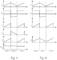
- the structure of an exemplary embodiment of a corresponding circuit and its function are further down the hand of the Fig. 1 and Fig. 3 described.
- Prior art switching transducers of the prior art not only require a series inductance, but also a freewheeling diode and a storage capacity.
- the cost of these components are disproportionately significant in the power supply of cost-effective LED arrays, for example, from a car electrical system, so that an object of the invention is to find a simpler and cheaper solution for such switching converters.
- the current sensor is a resistor which detects the total current through the LED series circuit and the switching transistor.
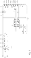
- FIG. 1 there is shown a series connection of a number of LEDs LED1 to LEDn , generally LEDi , in the present example seven LEDs.
- LEDi a number of LEDs LED1 to LEDn
- the term series connection of LEDs should also include arrangements in which also parallel circuits of LEDs are connected in series, which means that instead of one LED, for example LED1, two or more LEDs connected in parallel could be located.
- This series circuit is fed by a switching converter 1 with a current I , wherein the input of the switching converter is connected to an input voltage U E , which corresponds for example substantially to the battery voltage U B of a motor vehicle.
- an upstream network which as here filter capacitors C1, C2, C3 and C4 , filter resistors R1 , R2 , a Verpoltikdiode D1 and an overvoltage protection D2 contains.
- the switching converter has a longitudinal inductance L , which lies between a first pole, in this case the positive pole of the input voltage U E , and a first terminal of the LED series circuit LED1 ... LEDn, the second terminal of the LED series circuit having the second pole of the input voltage U E is connected.
- a first terminal of the series inductance L is connected to the input voltage U E , its other terminal leads via a freewheeling diode D to a charging capacitor C L 1 .
- a filter inductor L F another capacitor C L 2 downstream, to which the LED series circuit LED1 ... LEDn is connected in parallel.
- Another essential element of the switching converter is a switching transistor T , which is driven by a PWM drive circuit IC , wherein the switching transistor T, the longitudinal inductance L via the current sensor R periodically connects to the second pole of the input voltage U E.
- This drive circuit IC is the signal S of a current sensor R , here designed as an ohmic resistance, supplied, which is traversed by the current I T through the switching transistor and which images a current signal proportional to this voltage.
- the drive circuit IC which is for example a commercial product available under the designation MLX10803, high power LED driver of the company Melexis®, is externally connected to three resistors R3, R4, R5 and a capacitor C5, wherein the resistors R4 and R5 substantially specify an internal reference voltage for comparison with the signal s supplied to the drive circuit. If the voltage across the current sensor R - signal s - greater than the reference voltage, in the objective block is greater than half the reference voltage, the switching transistor T is opened, it is smaller, the transistor T is turned on.
- Phase 1 the transistor T turns on and applies the series inductance L to the input voltage U E.
- the series inductance a linearly increasing current I L flows and energy is stored in the magnetic field of the longitudinal inductance.
- the freewheeling diode D blocks because the voltage at the cathode is higher than at the anode.
- the current I for the LEDs LED1 ... LEDn is taken from the capacitors C L 1 and C L 2.
- the transistor T is switched off.
- Phase 2 In a second phase (“Phase 2") rises after locking of the transistor T, the voltage at the freewheeling diode D immediately at the level of the input voltage U E.
- the freewheeling diode D still locks because the voltage at the cathode is even higher than at the anode. Since no current flows anymore, the magnetic field collapses in the longitudinal inductance L and induces a high voltage, which adds to the input voltage U E. Since the two capacitors C L 1 and C L 2 were partially discharged in the phase 1, the voltage at the cathode of the diode D is lower than the now very high voltage at the anode. The diode D is immediately conductive and charges C to the increased by the induction voltage input voltage U E. With the renewed switching of the transistor T, the freewheeling diode D locks again and a new charging phase begins.
- FIG. 2 shows an embodiment of a switching converter according to the invention.
- the longitudinal inductance L corresponds to the switching converter that after Fig. 1 according to the prior art. However, it eliminates the freewheeling diode, the charging capacitor, the filter choke and the other capacitor.
- the series inductance L is rather directly connected to the one terminal of the series connection of the LEDs LED1 ... LEDn.
- the switching transistor T periodically connects the series inductance L to the second pole of the input voltage in the invention with the interposition of the first k LEDs LED1 and LED2. This is another significant difference from the prior art.
- the current sensor R may also be located at a different location of the series circuit of series inductance and LEDs, in order to accommodate a certain type of drive circuit IC.
- FIG. 4 Referred to - together with Fig. 2 - To explain the function of the switching converter according to the invention.
- Phase 1 the transistor T turns on and applies the longitudinal inductance L and the first k LEDs, LED1 and LED2, to the input voltage U E.
- Phase 2 increases after locking of the transistor T, the voltage at the LED series circuit LEDs LED1 ... LEDn immediately at the level of the input voltage U E. Since there is a higher voltage than the input voltage U E at the seven or n LEDs, no current flows. The magnetic field in the longitudinal inductance L collapses as current stops flowing and induces a high voltage which adds to the input voltage. The LEDs start to light up because the input voltage U E and the voltage generated by induction in the series inductance are high enough, so that a current flows through the LEDs until the energy stored in the series inductance L is used up and the LEDs no longer light up. With the renewed switching of the transistor T again begins the phase. 1
- the k LEDs here LED1 and LED2, which are connected to the input voltage UE via the transistor T in phase 1, must have a lower forward voltage than the minimum possible operating voltage.
- the five LEDs LED3 ... LEDn with n 7, it holds that their number can be arbitrary in principle, however, the number must be at least so large that the maximum operating voltage UE is lower than that Forward voltage of all, here seven, LEDs.
- the operating voltage UB be between 9 and 16 volts and the forward voltage of the LEDs should be between 2.5 and 3.5 volts. Then in phase 1, the voltage at the series connection of the LEDs between 5 and 7 volts and in phase 2 between 17.5 and 24.5 volts.
- the brightness of the nk LEDs LED3 ... LEDn in the “Phase 2" is naturally lower than the brightness of the k LEDs LED1, LED2 in “Phase1", but has been shown That this hardly plays a role in practice. Moreover, one could consider this fact by using different LED types.
Landscapes
- Dc-Dc Converters (AREA)
- Power Conversion In General (AREA)
Abstract
Description
- Die Erfindung bezieht sich auf einen Schaltwandler zum Speisen einer LED-Serienschaltung, mit einer Längsinduktivität, welche zwischen einem ersten Pol einer Eingangsspannung und einem ersten Anschluss der LED-Serienschaltung liegt, wobei der zweite Anschluss der LED-Serienschaltung mit dem zweiten Pol der Eingangsspannung verbunden ist, und mit einem Schalttransistor, welcher von einer PWM-Ansteuerschaltung angesteuert ist, welcher das Signal eines Stromsensors für einen Gesamtstrom durch die LED-Serienschaltung und den Schalttransistor zugeführt ist, wobei der Schalttransistor einen Anschluss der Längsinduktivität periodisch mit dem zweiten Pol der Eingangsspannung verbindet.
- Schaltwandler dieser Art gehören dem Stand der Technik an und sind dem Fachmann in vielen Varianten wohl bekannt. Der Aufbau einer beispielsweisen Ausführung einer entsprechenden Schaltung und deren Funktion sind weiter unten an Hand der
Fig. 1 undFig. 3 beschrieben. - Schaltwandler der gegenständlichen Art nach dem Stand der Technik benötigen nicht nur eine Längsinduktivität, sondern auch eine Freilaufdiode und eine Speicherkapazität. Die Kosten für diese Bauteile fallen jedoch bei der Stromversorgung kostengünstiger LED-Anordnungen, beispielsweise aus einem KFZ-Stromnetz, unverhältnismäßig stark ins Gewicht, sodass eine Aufgabe der Erfindung darin liegt, eine einfachere und billigere Lösung für solche Schaltwandler zu finden.
- Diese Aufgabe wird mit einem Schaltwandler der eingangs genannten Art gelöst, bei welchem erfindungsgemäß die Längsinduktivität direkt mit dem ersten Anschluss der LED-Serienschaltung verbunden ist und die Schaltstrecke des Schalttransistors lediglich eine erste Anzahl der LEDs überbrückt, wobei eine zweite Anzahl von LEDs, die von der Schaltstrecke des Schalttransistors nicht überbrückt sind, in Serie mit den von der Schaltstrecke überbrückten LEDs liegen.
- Dank der Erfindung können gegenüber dem Stand der Technik vergleichsweise teure Bauteile eingespart werden, sodass ein billiger Schaltwandler für die Ansteuerung von LED-Serienschaltungen geschaffen wird.
- Bei einer günstigen Ausführungsform ist vorgesehen, dass der Stromsensor ein Widerstand ist, welcher den Gesamtstrom durch die LED-Serienschaltung und den Schalttransistor erfasst.
- Die Erfindung bzw. der Stand der Technik als Ausgangspunkt der Erfindung sind im Folgenden an Hand von Ausführungsbeispielen unter Bezugnahme auf die Zeichnung näher erläutert. In dieser zeigen
-
Fig.1 eine beispielsweise Schaltung eines Schaltwandlers nach dem Stand der Technik, -
Fig.2 eine Schaltung eines Schaltwandlers nach einem Ausführungsbeispiel der Erfindung, -
Fig. 3 den Verlauf wesentlicher Ströme und Spannungen bei dem Schaltwandler nachFig. 1 und -
Fig. 4 den Verlauf wesentlicher Ströme und Spannungen bei dem erfindungsgemäßen Schaltwandler nachFig. 2 . - Es sei vorangestellt, dass zur Vereinfachung und zum Erleichtern der Verständlichkeit in den Figuren für gleiche oder gleichartige Bauteile, Schaltelemente und elektrische Größen gleiche Bezugszeichen verwendet werden.
- Nun auf
Fig. 1 Bezug nehmend erkennt man eine Serienschaltung einer Anzahl von LEDs LED1 bis LEDn, allgemein LEDi, im vorliegenden Beispiel sieben LEDs. Wenngleich nicht dargestellt, soll der Begriff Serienschaltung von LEDs auch Anordnungen umfassen, bei welchen auch Parallelschaltungen von LEDs in Serie geschaltet sind, was bedeutet, dass an Stelle einer LED, z.B. der LED1 zwei oder mehr parallelgeschaltete LEDs liegen könnten. - Diese Serienschaltung wird von einem Schaltwandler 1 mit einem Strom I gespeist, wobei der Eingang des Schaltwandlers an einer Eingangsspannung UE liegt, die beispielsweise im Wesentlichen der Batteriespannung UB eines Kraftfahrzeuges entspricht. Zwischen der Batteriespannung UB und dem Eingang des Schaltwandlers 1 liegt üblicherweise ein vorgeschaltetes Netzwerk, welches wie hier Filterkondensatoren C1, C2, C3 und C4, Filterwiderstände R1, R2, eine Verpolschutzdiode D1 und einen Überspannungsschutz D2 enthält.
- Der Schaltwandler besitzt eine Längsinduktivität L, welche zwischen einem ersten Pol, hier dem Pluspol der Eingangsspannung UE, und einem ersten Anschluss der LED-Serienschaltung LED1...LEDn liegt, wobei der zweite Anschluss der LED-Serienschaltung mit dem zweiten Pol der Eingangsspannung UE verbunden ist. Ein erster Anschluss der Längsinduktivität L liegt an der Eingangsspannung UE, ihr anderer Anschluss führt über eine Freilaufdiode D zu einem Ladekondensator CL1. Diesem ist über eine Filterdrossel LF ein weiterer Kondensator CL2 nachgeordnet, zu dem parallel die LED-Serienschaltung LED1...LEDn geschaltet ist.
- Ein weiteres wesentliches Element des Schaltwandlers ist ein Schalttransistor T, welcher von einer PWM-Ansteuerschaltung IC angesteuert ist, wobei der Schalttransistor T die Längsinduktivität L über den Stromsensor R periodisch mit dem zweiten Pol der Eingangsspannung UE verbindet. Dieser Ansteuerschaltung IC ist das Signal s eines Stromsensors R, hier als ohmscher Widerstand ausgebildet, zugeführt, welcher von dem Strom IT durch den Schalttransistor durchflossen ist und der ein diesem Strom proportionales Spannungssignal abbildet. Die Ansteuerschaltung IC, die beispielsweise ein unter der Bezeichnung MLX10803, high power LED Driver der Firma Melexis® erhältliches, handelsübliches Produkt ist, ist außen mit drei Widerständen R3, R4, R5 und einem Kondensator C5 beschaltet, wobei die Widerstände R4 und R5 im Wesentlichen eine interne Referenzspannung zum Vergleich mit dem der Ansteuerschaltung zugeführten Signal s festlegen. Wenn die Spannung an dem Stromsensor R - Signal s - größer als die Referenzspannung, bei dem gegenständlichen Baustein größer als die halbe Referenzspannung ist, wird der Schalttransistor T geöffnet, ist sie kleiner, so wird der Transistor T durchgeschaltet.
- Nun wird unter Bezugnahme auch auf
Fig. 3 die Funktion dieses bekannten Schaltwandlers erläutert, um später die Unterschiede zwischen Stand der Technik und der Erfindung besser hervorheben zu können. - In einer ersten Phase ("Phase1") schaltet der Transistor T durch und legt die Längsinduktivität L an die Eingangsspannung UE. Durch die Längsinduktivität fließt ein linear ansteigender Strom IL und im Magnetfeld der Längsinduktivität wird Energie gespeichert. Die Freilaufdiode D sperrt, da an der Kathode die Spannung höher ist als an der Anode. In dieser Phase wird der Strom I für die LEDs LED1...LEDn aus den Kondensatoren CL1 und CL2 entnommen. Sobald der Ladestrom den maximal festgelegten Strom durch die Längsinduktivität L, der mit Hilfe des Stromsensors R gemessen wird, erreicht hat, wird der Transistor T abgeschaltet.
- In einer zweiten Phase ("Phase2") steigt nach Sperren des Transistors T die Spannung an der Freilaufdiode D sofort auf Höhe der Eingangsspannung UE. Die Freilaufdiode D sperrt noch immer, da die Spannung an der Kathode noch höher ist als an der Anode. Da kein Strom mehr fließt bricht das Magnetfeld in der Längsinduktivität L zusammen und induziert eine hohe Spannung, die sich zu der Eingangsspannung UE addiert. Da die beiden Kondensatoren CL1 und CL2 in der Phase 1 teilweise entladen wurden, ist die Spannung an der Kathode der Diode D niedriger als die nun sehr hohe Spannung an der Anode. Die Diode D wird sofort leitend und lädt C auf die um die Induktionsspannung aufgestockte Eingangsspannung UE auf. Mit dem erneuten Durchschalten des Transistors T sperrt die Freilaufdiode D wieder und eine neue Ladephase beginnt.
- Nun wird auf
Fig. 2 Bezug genommen, welche eine Ausführungsform eines erfindungsgemäßen Schaltwandlers zeigt. Eingangsseitig, einschließlich der Ansteuerschaltung IC und der Längsinduktivität L entspricht der Schaltwandler jenem nachFig. 1 entsprechend dem Stand der Technik. Es entfallen jedoch die Freilaufdiode, der Ladekondensator, die Filterdrossel und der weitere Kondensator. Die Längsinduktivität L ist vielmehr unmittelbar mit dem einen Anschluss der Serienschaltung der LEDs LED1...LEDn verbunden. - Die Schaltstrecke des Transistors T liegt, wieder unter Zwischenschaltung des Stromsensors R, einerseits an dem zweiten Pol der Eingangsspannung UE und andererseits am Verbindungspunkt der ersten k LEDs, hier mit k=2 der LED1 und der LED2. Die Schaltstrecke des Transistors T überbrückt somit die restlichen LEDs, hier mit n=7 und n-k=5, somit die LED3 bis LED7. Der Schalttransistor T verbindet die Längsinduktivität L periodisch mit dem zweiten Pol der Eingangsspannung bei der Erfindung unter Zwischenschaltung der ersten k LEDs LED1 und LED2. Dies ist ein weiterer wesentlicher Unterschied gegenüber dem Stand der Technik.
- Man erkennt bei einem Vergleich der
Fig. 1 mitFig. 2 , dass bei der Erfindung die Ladekondensatoren CL1 und CL2 derFig. 1 entfallen, welche dort zum Zwischenspeichern der Energie notwendig sind, damit die LEDs auch während der Phase 1 leuchten. Ebenso entfällt die Freilaufdiode D und die Filterdrossel LF derFig. 1 . - Natürlich kann der Stromsensor R auch an einer anderen Stelle der Serienschaltung von Längsinduktivität und LEDs liegen, um einer bestimmten Bauart der Ansteuerschaltung IC, entgegenzukommen.
- Nun wird auf
Fig. 4 Bezug genommen, um - zusammen mitFig. 2 - die Funktion des Schaltwandlers nach der Erfindung zu erläutern. - In einer ersten Phase ("Phase1") schaltet der Transistor T durch und legt die Längsinduktivität L und die ersten k LEDs, LED1 und LED2, an die Eingangsspannung UE.
- Durch die Längsinduktivität L fließt ein linear ansteigender Strom und in ihrem Magnetfeld wird Energie gespeichert. In dieser Phase leuchten nur die ersten k, hier zwei LEDs und durch die restlichen (n-k), hier fünf LEDs fließt kein Strom. Sobald der Ladestrom den maximal festgelegten Strom durch die Längsinduktivität L, der mit Hilfe des Stromsensors R gemessen wird, erreicht hat, wird der Transistor T abgeschaltet.
- In der zweiten Phase ("Phase 2") steigt nach Sperren des Transistors T die Spannung an der LED-Serienschaltung LEDs LED1...LEDn sofort auf Höhe der Eingangsspannung UE. Da an den sieben bzw. n LEDs eine höhere Spannung als die Eingangsspannung UE liegt, fließt kein Strom. Das Magnetfeld in der Längsinduktivität L bricht, da kein Strom mehr fließt, zusammen und induziert eine hohe Spannung, die sich zu der Eingangsspannung addiert. Die LEDs beginnen zu leuchten da die Eingangsspannung UE und die durch Induktion in der Längsinduktivität erzeugte Spannung hoch genug ist, sodass demnach durch die LEDs ein Strom fließt, bis die in der Längsinduktivität L gespeicherte Energie aufgebraucht ist und die LEDs nicht mehr leuchten. Mit dem erneuten Durchschalten des Transistors T beginnt wiederum die Phase 1.
- Was die Anzahl der LEDs und die Dimensionierungsgrundsätze betrifft, so müssen die k LEDs, hier LED1 und LED2, die über den Transistor T in Phase 1 an die Eingangsspannung UE gelegt werden, eine geringere Flussspannung aufweisen, als die minimal mögliche Betriebsspannung. Für die restlichen n-k LEDs, hier die fünf LEDs LED3...LEDn mit n=7, gilt, dass deren Anzahl im Prinzip beliebig sein kann, jedoch muss die Anzahl zumindest so groß sein, dass die maximale Betriebsspannung UE niedriger ist, als die Flussspannung sämtlicher, hier sieben, LEDs.
- Bei einem praktischen Beispiel möge die Betriebsspannung UB zwischen 9 und 16 Volt betragen und die Flussspannung der LEDs möge zwischen 2,5 und 3,5 Volt liegen. Dann liegt in Phase 1 die Spannung an der Serienschaltung der LEDs zwischen 5 und 7 Volt und in Phase 2 zwischen 17,5 und 24,5 Volt.
- Es soll darauf hingewiesen werden, dass bei Verwendung eines erfindungsgemäßen Schaltwandlers die Helligkeit der n-k LEDs LED3...LEDn in der "Phase 2" naturgemäß geringer ist, als die Helligkeit der k LEDs LED1, LED2 in "Phase1", doch hat sich gezeigt, dass dies in der Praxis kaum eine Rolle spielt. Überdies könnte man diesen Umstand durch Verwendung unterschiedlicher LED-Typen berücksichtigen.
- Da bei der Erfindung die Ladekondensatoren entfallen, ist auch keine Filterdrossel mehr erforderlich und die elektromagnetischen Störungen werden geringer, da in der Schaltung keine Ströme mit steilen Flanken fließen. Wegen des Entfalls der Ladekondensatoren ist auch die Freilaufdiode nicht mehr erforderlich.
-
- 1
- Schaltwandler
- C1...C4
- Filterkondensatoren
- CL1
- Ladekondensator
- CL2
- Kondensator
- C5
- Kondensator
- D
- Freilaufdiode
- D1
- Verpolschutzdiode
- D2
- Überspannungsschutz
- IC
- Ansteuerschaltung
- I
- Strom durch Serienschaltung
- ID
- Strom durch Diode
- IL
- Strom durch Längsinduktivität
- IT
- Strom durch den Schalttransistor
- LEDi
- Leuchtdioden
- L
- Längsinduktivität
- LF
- Filterdrossel
- R
- Stromsensor
- R1, R2
- Filterwiderstände
- R3...R5
- Widerstände
- s
- Signal
- T
- Schalttransistor
- UB
- Betriebsspannung
- UCD
- Spannung
- UE
- Eingangsspannung
Claims (2)
- Schaltwandler zum Speisen einer LED-Serienschaltung (LED1...LEDn), mit einer Längsinduktivität (L), welche zwischen einem ersten Pol einer Eingangsspannung (UE) und einem ersten Anschluss der LED-Serienschaltung liegt, wobei der zweite Anschluss der LED-Serienschaltung mit dem zweiten Pol der Eingangsspannung verbunden ist, und mit einem Schalttransistor (T), welcher von einer PWM-Ansteuerschaltung (IC) angesteuert ist, welcher das Signal eines Stromsensors (R) für einen Gesamtstrom durch die LED-Serienschaltung und den Schalttransistor zugeführt ist, wobei der Schalttransistor einen Anschluss der Längsinduktivität periodisch mit dem zweiten Pol der Eingangsspannung verbindet,
dadurch gekennzeichnet, dass
die Längsinduktivität (L) direkt mit dem ersten Anschluss der LED-Serienschaltung (LED1...LEDn) verbunden ist und die Schaltstrecke des Schalttransistors lediglich eine erste Anzahl (n-k) der LEDs überbrückt, wobei eine zweite Anzahl (k) von LEDs (LED1, LED2), die von der Schaltstrecke des Schalttransistors (T) nicht überbrückt sind, in Serie mit den von der Schaltstrecke überbrückten LEDs (LED3...LEDn) liegen. - Schaltwandler nach Anspruch 1, dadurch gekennzeichnet, dass der Stromsensor (R) ein Widerstand ist, welcher den Gesamtstrom durch die LED-Serienschaltung (LED1...LEDn) und den Schalttransistor (T) erfasst.
Priority Applications (1)
| Application Number | Priority Date | Filing Date | Title |
|---|---|---|---|
| EP17211061.1A EP3506723B1 (de) | 2017-12-29 | 2017-12-29 | Schaltwandler zum speisen einer led-serienschaltung |
Applications Claiming Priority (1)
| Application Number | Priority Date | Filing Date | Title |
|---|---|---|---|
| EP17211061.1A EP3506723B1 (de) | 2017-12-29 | 2017-12-29 | Schaltwandler zum speisen einer led-serienschaltung |
Publications (2)
| Publication Number | Publication Date |
|---|---|
| EP3506723A1 true EP3506723A1 (de) | 2019-07-03 |
| EP3506723B1 EP3506723B1 (de) | 2022-12-21 |
Family
ID=60856945
Family Applications (1)
| Application Number | Title | Priority Date | Filing Date |
|---|---|---|---|
| EP17211061.1A Active EP3506723B1 (de) | 2017-12-29 | 2017-12-29 | Schaltwandler zum speisen einer led-serienschaltung |
Country Status (1)
| Country | Link |
|---|---|
| EP (1) | EP3506723B1 (de) |
Cited By (1)
| Publication number | Priority date | Publication date | Assignee | Title |
|---|---|---|---|---|
| CN110730540A (zh) * | 2019-10-17 | 2020-01-24 | 横店集团得邦照明股份有限公司 | 一种采用电感串联方式的led电路及其实现方法 |
Citations (1)
| Publication number | Priority date | Publication date | Assignee | Title |
|---|---|---|---|---|
| US20170066366A1 (en) * | 2015-09-08 | 2017-03-09 | MLS Automotive Inc. | Systems and methods for vehicle lighting |
-
2017
- 2017-12-29 EP EP17211061.1A patent/EP3506723B1/de active Active
Patent Citations (1)
| Publication number | Priority date | Publication date | Assignee | Title |
|---|---|---|---|---|
| US20170066366A1 (en) * | 2015-09-08 | 2017-03-09 | MLS Automotive Inc. | Systems and methods for vehicle lighting |
Non-Patent Citations (1)
| Title |
|---|
| MELEXIS: "FACT PAGE Power supply/LED drivers", 1 July 2007 (2007-07-01), XP055475434, Retrieved from the Internet <URL:https://www.melexis.com/-/media/files/documents/whitepapers/power-supply-led-drivers-whitepaper-melexis.pdf> [retrieved on 20180516] * |
Cited By (1)
| Publication number | Priority date | Publication date | Assignee | Title |
|---|---|---|---|---|
| CN110730540A (zh) * | 2019-10-17 | 2020-01-24 | 横店集团得邦照明股份有限公司 | 一种采用电感串联方式的led电路及其实现方法 |
Also Published As
| Publication number | Publication date |
|---|---|
| EP3506723B1 (de) | 2022-12-21 |
Similar Documents
| Publication | Publication Date | Title |
|---|---|---|
| WO2000044048A1 (de) | Hybrid-leistungs-mosfet | |
| DE102013217037B3 (de) | Vorrichtung zum Laden und Entladen eines kapazitiven Stellgliedes und Anordnung mit einer solchen Vorrichtung | |
| DE2320128C3 (de) | Zerhacker | |
| DE102006010528A1 (de) | Batterie-Verpolschutz durch Nmos | |
| AT518423A4 (de) | Kraftfahrzeug-Beleuchtungseinrichtung | |
| DE19704089A1 (de) | Verfahren zur Steuerung eines Zerhacker(Chopper)-Treibers und Schaltungsanordnung zur Durchführung des Verfahrens | |
| DE4031288C1 (en) | Incorrect polarity protection CCT - has drain-source connected into minus or positive line between DC source | |
| DE102014202617B4 (de) | Verfahren und Vorrichtung zum Messen eines Batteriezellenstromes | |
| EP3506723B1 (de) | Schaltwandler zum speisen einer led-serienschaltung | |
| DE19732098A1 (de) | Steuerschaltung für einen Gleichstrommotor | |
| DE102018220247A1 (de) | Leistungsschalteranordnung | |
| EP2822166A1 (de) | Eintakt-Durchflusswandler mit sekundärseitiger Snubberschaltung | |
| EP1195885B1 (de) | Synchrongleichrichterschaltung | |
| EP0849854A2 (de) | Elektronisches Schaltnetzteil | |
| EP0009225B1 (de) | Schutzbeschaltung | |
| EP0622902A2 (de) | Halbleiterrelais | |
| DE60013681T2 (de) | Ein Gleichspannungswandler mit mehrere Ausgängen, insbesondere zum Betrieb in Fahrzeugen | |
| EP0489935B1 (de) | MOSFET-Schalter für eine induktive Last | |
| DE3335475A1 (de) | Schalter mit in serie geschalteten feldeffekttransistoren | |
| DE102013218799A1 (de) | Modularer Stromrichter | |
| DE102006058725A1 (de) | Schaltungsanordnung zur gemeinsamen Pulsweitenmodulation von Ventilen mit Löschung | |
| DE202008006853U1 (de) | Elektronisch kommutierter Gleichstrommotor mit einem pi-Filter | |
| DE102008043424A1 (de) | Motoransteuerungsspannungsversorgungsschaltung mit einem EMV-Filter und einem Verpolschutz | |
| DE102011011295A1 (de) | Stromversorgungsanordnung für ohmsch-induktiven Verbraucher | |
| DE10127868A1 (de) | Bootstrap-Spannungsversorgung |
Legal Events
| Date | Code | Title | Description |
|---|---|---|---|
| PUAI | Public reference made under article 153(3) epc to a published international application that has entered the european phase |
Free format text: ORIGINAL CODE: 0009012 |
|
| STAA | Information on the status of an ep patent application or granted ep patent |
Free format text: STATUS: THE APPLICATION HAS BEEN PUBLISHED |
|
| AK | Designated contracting states |
Kind code of ref document: A1 Designated state(s): AL AT BE BG CH CY CZ DE DK EE ES FI FR GB GR HR HU IE IS IT LI LT LU LV MC MK MT NL NO PL PT RO RS SE SI SK SM TR |
|
| AX | Request for extension of the european patent |
Extension state: BA ME |
|
| STAA | Information on the status of an ep patent application or granted ep patent |
Free format text: STATUS: REQUEST FOR EXAMINATION WAS MADE |
|
| 17P | Request for examination filed |
Effective date: 20191220 |
|
| RBV | Designated contracting states (corrected) |
Designated state(s): AL AT BE BG CH CY CZ DE DK EE ES FI FR GB GR HR HU IE IS IT LI LT LU LV MC MK MT NL NO PL PT RO RS SE SI SK SM TR |
|
| STAA | Information on the status of an ep patent application or granted ep patent |
Free format text: STATUS: EXAMINATION IS IN PROGRESS |
|
| 17Q | First examination report despatched |
Effective date: 20210202 |
|
| REG | Reference to a national code |
Ref country code: DE Ref legal event code: R079 Ref document number: 502017014238 Country of ref document: DE Free format text: PREVIOUS MAIN CLASS: H05B0033080000 Ipc: H05B0045480000 |
|
| GRAP | Despatch of communication of intention to grant a patent |
Free format text: ORIGINAL CODE: EPIDOSNIGR1 |
|
| STAA | Information on the status of an ep patent application or granted ep patent |
Free format text: STATUS: GRANT OF PATENT IS INTENDED |
|
| RIC1 | Information provided on ipc code assigned before grant |
Ipc: H05B 45/3725 20200101ALI20220908BHEP Ipc: H05B 45/48 20200101AFI20220908BHEP |
|
| INTG | Intention to grant announced |
Effective date: 20220928 |
|
| GRAS | Grant fee paid |
Free format text: ORIGINAL CODE: EPIDOSNIGR3 |
|
| GRAA | (expected) grant |
Free format text: ORIGINAL CODE: 0009210 |
|
| STAA | Information on the status of an ep patent application or granted ep patent |
Free format text: STATUS: THE PATENT HAS BEEN GRANTED |
|
| AK | Designated contracting states |
Kind code of ref document: B1 Designated state(s): AL AT BE BG CH CY CZ DE DK EE ES FI FR GB GR HR HU IE IS IT LI LT LU LV MC MK MT NL NO PL PT RO RS SE SI SK SM TR |
|
| REG | Reference to a national code |
Ref country code: GB Ref legal event code: FG4D Free format text: NOT ENGLISH |
|
| REG | Reference to a national code |
Ref country code: CH Ref legal event code: EP |
|
| REG | Reference to a national code |
Ref country code: DE Ref legal event code: R096 Ref document number: 502017014238 Country of ref document: DE |
|
| REG | Reference to a national code |
Ref country code: AT Ref legal event code: REF Ref document number: 1539837 Country of ref document: AT Kind code of ref document: T Effective date: 20230115 |
|
| REG | Reference to a national code |
Ref country code: IE Ref legal event code: FG4D Free format text: LANGUAGE OF EP DOCUMENT: GERMAN |
|
| REG | Reference to a national code |
Ref country code: LT Ref legal event code: MG9D |
|
| REG | Reference to a national code |
Ref country code: NL Ref legal event code: MP Effective date: 20221221 |
|
| PG25 | Lapsed in a contracting state [announced via postgrant information from national office to epo] |
Ref country code: SE Free format text: LAPSE BECAUSE OF FAILURE TO SUBMIT A TRANSLATION OF THE DESCRIPTION OR TO PAY THE FEE WITHIN THE PRESCRIBED TIME-LIMIT Effective date: 20221221 Ref country code: NO Free format text: LAPSE BECAUSE OF FAILURE TO SUBMIT A TRANSLATION OF THE DESCRIPTION OR TO PAY THE FEE WITHIN THE PRESCRIBED TIME-LIMIT Effective date: 20230321 Ref country code: LT Free format text: LAPSE BECAUSE OF FAILURE TO SUBMIT A TRANSLATION OF THE DESCRIPTION OR TO PAY THE FEE WITHIN THE PRESCRIBED TIME-LIMIT Effective date: 20221221 Ref country code: FI Free format text: LAPSE BECAUSE OF FAILURE TO SUBMIT A TRANSLATION OF THE DESCRIPTION OR TO PAY THE FEE WITHIN THE PRESCRIBED TIME-LIMIT Effective date: 20221221 |
|
| PG25 | Lapsed in a contracting state [announced via postgrant information from national office to epo] |
Ref country code: RS Free format text: LAPSE BECAUSE OF FAILURE TO SUBMIT A TRANSLATION OF THE DESCRIPTION OR TO PAY THE FEE WITHIN THE PRESCRIBED TIME-LIMIT Effective date: 20221221 Ref country code: LV Free format text: LAPSE BECAUSE OF FAILURE TO SUBMIT A TRANSLATION OF THE DESCRIPTION OR TO PAY THE FEE WITHIN THE PRESCRIBED TIME-LIMIT Effective date: 20221221 Ref country code: HR Free format text: LAPSE BECAUSE OF FAILURE TO SUBMIT A TRANSLATION OF THE DESCRIPTION OR TO PAY THE FEE WITHIN THE PRESCRIBED TIME-LIMIT Effective date: 20221221 Ref country code: GR Free format text: LAPSE BECAUSE OF FAILURE TO SUBMIT A TRANSLATION OF THE DESCRIPTION OR TO PAY THE FEE WITHIN THE PRESCRIBED TIME-LIMIT Effective date: 20230322 |
|
| PG25 | Lapsed in a contracting state [announced via postgrant information from national office to epo] |
Ref country code: NL Free format text: LAPSE BECAUSE OF FAILURE TO SUBMIT A TRANSLATION OF THE DESCRIPTION OR TO PAY THE FEE WITHIN THE PRESCRIBED TIME-LIMIT Effective date: 20221221 |
|
| P01 | Opt-out of the competence of the unified patent court (upc) registered |
Effective date: 20230528 |
|
| PG25 | Lapsed in a contracting state [announced via postgrant information from national office to epo] |
Ref country code: SM Free format text: LAPSE BECAUSE OF FAILURE TO SUBMIT A TRANSLATION OF THE DESCRIPTION OR TO PAY THE FEE WITHIN THE PRESCRIBED TIME-LIMIT Effective date: 20221221 Ref country code: RO Free format text: LAPSE BECAUSE OF FAILURE TO SUBMIT A TRANSLATION OF THE DESCRIPTION OR TO PAY THE FEE WITHIN THE PRESCRIBED TIME-LIMIT Effective date: 20221221 Ref country code: PT Free format text: LAPSE BECAUSE OF FAILURE TO SUBMIT A TRANSLATION OF THE DESCRIPTION OR TO PAY THE FEE WITHIN THE PRESCRIBED TIME-LIMIT Effective date: 20230421 Ref country code: ES Free format text: LAPSE BECAUSE OF FAILURE TO SUBMIT A TRANSLATION OF THE DESCRIPTION OR TO PAY THE FEE WITHIN THE PRESCRIBED TIME-LIMIT Effective date: 20221221 Ref country code: EE Free format text: LAPSE BECAUSE OF FAILURE TO SUBMIT A TRANSLATION OF THE DESCRIPTION OR TO PAY THE FEE WITHIN THE PRESCRIBED TIME-LIMIT Effective date: 20221221 Ref country code: CZ Free format text: LAPSE BECAUSE OF FAILURE TO SUBMIT A TRANSLATION OF THE DESCRIPTION OR TO PAY THE FEE WITHIN THE PRESCRIBED TIME-LIMIT Effective date: 20221221 |
|
| REG | Reference to a national code |
Ref country code: CH Ref legal event code: PL |
|
| REG | Reference to a national code |
Ref country code: BE Ref legal event code: MM Effective date: 20221231 |
|
| PG25 | Lapsed in a contracting state [announced via postgrant information from national office to epo] |
Ref country code: SK Free format text: LAPSE BECAUSE OF FAILURE TO SUBMIT A TRANSLATION OF THE DESCRIPTION OR TO PAY THE FEE WITHIN THE PRESCRIBED TIME-LIMIT Effective date: 20221221 Ref country code: PL Free format text: LAPSE BECAUSE OF FAILURE TO SUBMIT A TRANSLATION OF THE DESCRIPTION OR TO PAY THE FEE WITHIN THE PRESCRIBED TIME-LIMIT Effective date: 20221221 Ref country code: LU Free format text: LAPSE BECAUSE OF NON-PAYMENT OF DUE FEES Effective date: 20221229 Ref country code: IS Free format text: LAPSE BECAUSE OF FAILURE TO SUBMIT A TRANSLATION OF THE DESCRIPTION OR TO PAY THE FEE WITHIN THE PRESCRIBED TIME-LIMIT Effective date: 20230421 Ref country code: AL Free format text: LAPSE BECAUSE OF FAILURE TO SUBMIT A TRANSLATION OF THE DESCRIPTION OR TO PAY THE FEE WITHIN THE PRESCRIBED TIME-LIMIT Effective date: 20221221 |
|
| REG | Reference to a national code |
Ref country code: DE Ref legal event code: R097 Ref document number: 502017014238 Country of ref document: DE |
|
| PG25 | Lapsed in a contracting state [announced via postgrant information from national office to epo] |
Ref country code: MC Free format text: LAPSE BECAUSE OF FAILURE TO SUBMIT A TRANSLATION OF THE DESCRIPTION OR TO PAY THE FEE WITHIN THE PRESCRIBED TIME-LIMIT Effective date: 20221221 |
|
| PLBE | No opposition filed within time limit |
Free format text: ORIGINAL CODE: 0009261 |
|
| STAA | Information on the status of an ep patent application or granted ep patent |
Free format text: STATUS: NO OPPOSITION FILED WITHIN TIME LIMIT |
|
| PG25 | Lapsed in a contracting state [announced via postgrant information from national office to epo] |
Ref country code: LI Free format text: LAPSE BECAUSE OF NON-PAYMENT OF DUE FEES Effective date: 20221231 Ref country code: IE Free format text: LAPSE BECAUSE OF NON-PAYMENT OF DUE FEES Effective date: 20221229 Ref country code: DK Free format text: LAPSE BECAUSE OF FAILURE TO SUBMIT A TRANSLATION OF THE DESCRIPTION OR TO PAY THE FEE WITHIN THE PRESCRIBED TIME-LIMIT Effective date: 20221221 Ref country code: CH Free format text: LAPSE BECAUSE OF NON-PAYMENT OF DUE FEES Effective date: 20221231 |
|
| 26N | No opposition filed |
Effective date: 20230922 |
|
| GBPC | Gb: european patent ceased through non-payment of renewal fee |
Effective date: 20230321 |
|
| PG25 | Lapsed in a contracting state [announced via postgrant information from national office to epo] |
Ref country code: BE Free format text: LAPSE BECAUSE OF NON-PAYMENT OF DUE FEES Effective date: 20221231 |
|
| PG25 | Lapsed in a contracting state [announced via postgrant information from national office to epo] |
Ref country code: GB Free format text: LAPSE BECAUSE OF NON-PAYMENT OF DUE FEES Effective date: 20230321 |
|
| PG25 | Lapsed in a contracting state [announced via postgrant information from national office to epo] |
Ref country code: SI Free format text: LAPSE BECAUSE OF FAILURE TO SUBMIT A TRANSLATION OF THE DESCRIPTION OR TO PAY THE FEE WITHIN THE PRESCRIBED TIME-LIMIT Effective date: 20221221 Ref country code: GB Free format text: LAPSE BECAUSE OF NON-PAYMENT OF DUE FEES Effective date: 20230321 |
|
| REG | Reference to a national code |
Ref country code: AT Ref legal event code: MM01 Ref document number: 1539837 Country of ref document: AT Kind code of ref document: T Effective date: 20221229 |
|
| PG25 | Lapsed in a contracting state [announced via postgrant information from national office to epo] |
Ref country code: HU Free format text: LAPSE BECAUSE OF FAILURE TO SUBMIT A TRANSLATION OF THE DESCRIPTION OR TO PAY THE FEE WITHIN THE PRESCRIBED TIME-LIMIT; INVALID AB INITIO Effective date: 20171229 |
|
| PG25 | Lapsed in a contracting state [announced via postgrant information from national office to epo] |
Ref country code: AT Free format text: LAPSE BECAUSE OF NON-PAYMENT OF DUE FEES Effective date: 20221229 |
|
| PG25 | Lapsed in a contracting state [announced via postgrant information from national office to epo] |
Ref country code: CY Free format text: LAPSE BECAUSE OF FAILURE TO SUBMIT A TRANSLATION OF THE DESCRIPTION OR TO PAY THE FEE WITHIN THE PRESCRIBED TIME-LIMIT Effective date: 20221221 Ref country code: AT Free format text: LAPSE BECAUSE OF NON-PAYMENT OF DUE FEES Effective date: 20221229 |
|
| PG25 | Lapsed in a contracting state [announced via postgrant information from national office to epo] |
Ref country code: MK Free format text: LAPSE BECAUSE OF FAILURE TO SUBMIT A TRANSLATION OF THE DESCRIPTION OR TO PAY THE FEE WITHIN THE PRESCRIBED TIME-LIMIT Effective date: 20221221 Ref country code: IT Free format text: LAPSE BECAUSE OF FAILURE TO SUBMIT A TRANSLATION OF THE DESCRIPTION OR TO PAY THE FEE WITHIN THE PRESCRIBED TIME-LIMIT Effective date: 20221221 |
|
| PG25 | Lapsed in a contracting state [announced via postgrant information from national office to epo] |
Ref country code: TR Free format text: LAPSE BECAUSE OF FAILURE TO SUBMIT A TRANSLATION OF THE DESCRIPTION OR TO PAY THE FEE WITHIN THE PRESCRIBED TIME-LIMIT Effective date: 20221221 |
|
| PG25 | Lapsed in a contracting state [announced via postgrant information from national office to epo] |
Ref country code: BG Free format text: LAPSE BECAUSE OF FAILURE TO SUBMIT A TRANSLATION OF THE DESCRIPTION OR TO PAY THE FEE WITHIN THE PRESCRIBED TIME-LIMIT Effective date: 20221221 |
|
| PG25 | Lapsed in a contracting state [announced via postgrant information from national office to epo] |
Ref country code: MT Free format text: LAPSE BECAUSE OF FAILURE TO SUBMIT A TRANSLATION OF THE DESCRIPTION OR TO PAY THE FEE WITHIN THE PRESCRIBED TIME-LIMIT Effective date: 20221221 |
|
| REG | Reference to a national code |
Ref country code: DE Ref legal event code: R084 Ref document number: 502017014238 Country of ref document: DE |
|
| PGFP | Annual fee paid to national office [announced via postgrant information from national office to epo] |
Ref country code: FR Payment date: 20251217 Year of fee payment: 9 |
|
| PGFP | Annual fee paid to national office [announced via postgrant information from national office to epo] |
Ref country code: DE Payment date: 20251222 Year of fee payment: 9 |