EP3501043B1 - Flexible verbindung - Google Patents
Flexible verbindung Download PDFInfo
- Publication number
- EP3501043B1 EP3501043B1 EP17761147.2A EP17761147A EP3501043B1 EP 3501043 B1 EP3501043 B1 EP 3501043B1 EP 17761147 A EP17761147 A EP 17761147A EP 3501043 B1 EP3501043 B1 EP 3501043B1
- Authority
- EP
- European Patent Office
- Prior art keywords
- encapsulant
- liquid metal
- interconnect
- embedded
- magnetic
- Prior art date
- Legal status (The legal status is an assumption and is not a legal conclusion. Google has not performed a legal analysis and makes no representation as to the accuracy of the status listed.)
- Active
Links
Images



Classifications
-
- H—ELECTRICITY
- H05—ELECTRIC TECHNIQUES NOT OTHERWISE PROVIDED FOR
- H05K—PRINTED CIRCUITS; CASINGS OR CONSTRUCTIONAL DETAILS OF ELECTRIC APPARATUS; MANUFACTURE OF ASSEMBLAGES OF ELECTRICAL COMPONENTS
- H05K1/00—Printed circuits
- H05K1/02—Details
- H05K1/14—Structural association of two or more printed circuits
-
- H—ELECTRICITY
- H05—ELECTRIC TECHNIQUES NOT OTHERWISE PROVIDED FOR
- H05K—PRINTED CIRCUITS; CASINGS OR CONSTRUCTIONAL DETAILS OF ELECTRIC APPARATUS; MANUFACTURE OF ASSEMBLAGES OF ELECTRICAL COMPONENTS
- H05K1/00—Printed circuits
- H05K1/02—Details
- H05K1/0277—Bendability or stretchability details
- H05K1/0283—Stretchable printed circuits
-
- H—ELECTRICITY
- H05—ELECTRIC TECHNIQUES NOT OTHERWISE PROVIDED FOR
- H05K—PRINTED CIRCUITS; CASINGS OR CONSTRUCTIONAL DETAILS OF ELECTRIC APPARATUS; MANUFACTURE OF ASSEMBLAGES OF ELECTRICAL COMPONENTS
- H05K1/00—Printed circuits
- H05K1/02—Details
- H05K1/0296—Conductive pattern lay-out details not covered by sub groups H05K1/02 - H05K1/0295
-
- H—ELECTRICITY
- H05—ELECTRIC TECHNIQUES NOT OTHERWISE PROVIDED FOR
- H05K—PRINTED CIRCUITS; CASINGS OR CONSTRUCTIONAL DETAILS OF ELECTRIC APPARATUS; MANUFACTURE OF ASSEMBLAGES OF ELECTRICAL COMPONENTS
- H05K1/00—Printed circuits
- H05K1/02—Details
- H05K1/03—Use of materials for the substrate
- H05K1/0393—Flexible materials
-
- H—ELECTRICITY
- H05—ELECTRIC TECHNIQUES NOT OTHERWISE PROVIDED FOR
- H05K—PRINTED CIRCUITS; CASINGS OR CONSTRUCTIONAL DETAILS OF ELECTRIC APPARATUS; MANUFACTURE OF ASSEMBLAGES OF ELECTRICAL COMPONENTS
- H05K3/00—Apparatus or processes for manufacturing printed circuits
- H05K3/10—Apparatus or processes for manufacturing printed circuits in which conductive material is applied to the insulating support in such a manner as to form the desired conductive pattern
- H05K3/107—Apparatus or processes for manufacturing printed circuits in which conductive material is applied to the insulating support in such a manner as to form the desired conductive pattern by filling grooves in the support with conductive material
-
- H—ELECTRICITY
- H05—ELECTRIC TECHNIQUES NOT OTHERWISE PROVIDED FOR
- H05K—PRINTED CIRCUITS; CASINGS OR CONSTRUCTIONAL DETAILS OF ELECTRIC APPARATUS; MANUFACTURE OF ASSEMBLAGES OF ELECTRICAL COMPONENTS
- H05K3/00—Apparatus or processes for manufacturing printed circuits
- H05K3/22—Secondary treatment of printed circuits
- H05K3/28—Applying non-metallic protective coatings
-
- H—ELECTRICITY
- H10—SEMICONDUCTOR DEVICES; ELECTRIC SOLID-STATE DEVICES NOT OTHERWISE PROVIDED FOR
- H10W—GENERIC PACKAGES, INTERCONNECTIONS, CONNECTORS OR OTHER CONSTRUCTIONAL DETAILS OF DEVICES COVERED BY CLASS H10
- H10W70/00—Package substrates; Interposers; Redistribution layers [RDL]
- H10W70/01—Manufacture or treatment
- H10W70/05—Manufacture or treatment of insulating or insulated package substrates, or of interposers, or of redistribution layers
- H10W70/095—Manufacture or treatment of insulating or insulated package substrates, or of interposers, or of redistribution layers of vias therein
-
- H—ELECTRICITY
- H10—SEMICONDUCTOR DEVICES; ELECTRIC SOLID-STATE DEVICES NOT OTHERWISE PROVIDED FOR
- H10W—GENERIC PACKAGES, INTERCONNECTIONS, CONNECTORS OR OTHER CONSTRUCTIONAL DETAILS OF DEVICES COVERED BY CLASS H10
- H10W70/00—Package substrates; Interposers; Redistribution layers [RDL]
- H10W70/60—Insulating or insulated package substrates; Interposers; Redistribution layers
- H10W70/611—Insulating or insulated package substrates; Interposers; Redistribution layers for connecting multiple chips together
-
- H—ELECTRICITY
- H10—SEMICONDUCTOR DEVICES; ELECTRIC SOLID-STATE DEVICES NOT OTHERWISE PROVIDED FOR
- H10W—GENERIC PACKAGES, INTERCONNECTIONS, CONNECTORS OR OTHER CONSTRUCTIONAL DETAILS OF DEVICES COVERED BY CLASS H10
- H10W70/00—Package substrates; Interposers; Redistribution layers [RDL]
- H10W70/60—Insulating or insulated package substrates; Interposers; Redistribution layers
- H10W70/62—Insulating or insulated package substrates; Interposers; Redistribution layers characterised by their interconnections
- H10W70/66—Conductive materials thereof
- H10W70/662—Semiconductor materials
-
- H—ELECTRICITY
- H10—SEMICONDUCTOR DEVICES; ELECTRIC SOLID-STATE DEVICES NOT OTHERWISE PROVIDED FOR
- H10W—GENERIC PACKAGES, INTERCONNECTIONS, CONNECTORS OR OTHER CONSTRUCTIONAL DETAILS OF DEVICES COVERED BY CLASS H10
- H10W70/00—Package substrates; Interposers; Redistribution layers [RDL]
- H10W70/60—Insulating or insulated package substrates; Interposers; Redistribution layers
- H10W70/67—Insulating or insulated package substrates; Interposers; Redistribution layers characterised by their insulating layers or insulating parts
- H10W70/688—Flexible insulating substrates
-
- H—ELECTRICITY
- H05—ELECTRIC TECHNIQUES NOT OTHERWISE PROVIDED FOR
- H05K—PRINTED CIRCUITS; CASINGS OR CONSTRUCTIONAL DETAILS OF ELECTRIC APPARATUS; MANUFACTURE OF ASSEMBLAGES OF ELECTRICAL COMPONENTS
- H05K2201/00—Indexing scheme relating to printed circuits covered by H05K1/00
- H05K2201/03—Conductive materials
- H05K2201/032—Materials
-
- H—ELECTRICITY
- H05—ELECTRIC TECHNIQUES NOT OTHERWISE PROVIDED FOR
- H05K—PRINTED CIRCUITS; CASINGS OR CONSTRUCTIONAL DETAILS OF ELECTRIC APPARATUS; MANUFACTURE OF ASSEMBLAGES OF ELECTRICAL COMPONENTS
- H05K2201/00—Indexing scheme relating to printed circuits covered by H05K1/00
- H05K2201/03—Conductive materials
- H05K2201/0332—Structure of the conductor
- H05K2201/0388—Other aspects of conductors
- H05K2201/0391—Using different types of conductors
-
- H—ELECTRICITY
- H05—ELECTRIC TECHNIQUES NOT OTHERWISE PROVIDED FOR
- H05K—PRINTED CIRCUITS; CASINGS OR CONSTRUCTIONAL DETAILS OF ELECTRIC APPARATUS; MANUFACTURE OF ASSEMBLAGES OF ELECTRICAL COMPONENTS
- H05K2201/00—Indexing scheme relating to printed circuits covered by H05K1/00
- H05K2201/10—Details of components or other objects attached to or integrated in a printed circuit board
- H05K2201/10613—Details of electrical connections of non-printed components, e.g. special leads
- H05K2201/10954—Other details of electrical connections
- H05K2201/10977—Encapsulated connections
-
- H—ELECTRICITY
- H05—ELECTRIC TECHNIQUES NOT OTHERWISE PROVIDED FOR
- H05K—PRINTED CIRCUITS; CASINGS OR CONSTRUCTIONAL DETAILS OF ELECTRIC APPARATUS; MANUFACTURE OF ASSEMBLAGES OF ELECTRICAL COMPONENTS
- H05K2203/00—Indexing scheme relating to apparatus or processes for manufacturing printed circuits covered by H05K3/00
- H05K2203/13—Moulding and encapsulation; Deposition techniques; Protective layers
- H05K2203/1305—Moulding and encapsulation
Definitions
- Flexible electrical interconnects may be used to connect electronic components located in portions of a device that are moveable relative to one another.
- a flexible interconnect may be subject to a large number of flexing cycles over a lifetime of the device, and thus may be susceptible to damage.
- US 2013/243655 A1 discloses a flexible IC/microfluidic hybrid integration and packaging method and resulting device.
- a single flexible elastomer substrate such as polydimethylsiloxane (PDMS)
- PDMS polydimethylsiloxane
- liquid metals or low melting point solders
- the liquid metal used can be a gallium-indium-tin eutectic alloy (also called Galinstan).
- Examples are disclosed that relate to flexible electrical interconnects.
- One example provides an interconnect including a substrate, a liquid conductive pathway supported by the substrate, and a conductively anisotropic, magnetic particle-embedded encapsulant that interfaces with the liquid conductive pathway for connecting to another circuit element.
- Electrical interconnects may be incorporated into a variety of devices to provide electrical pathways between device components.
- Some electronic devices may include joints, hinges, and/or other moveable structures that connect two parts each having electronic components.
- a flexible interconnect may be utilized to bridge the components to allow the components to remain electrically interconnected as the components are moved relative to one another.
- Flexible interconnects are commonly formed from solid metal traces, such as copper, patterned on a flexible substrate, such as a polyimide film.
- the solid metal traces may fatigue over time after repeated flexing, which may lead to breakage of the traces, thereby disrupting the electrical connection between the components.
- Even solid metal traces that are able to withstand a high number of flex cycles may fail due to pinch points, strain, twist, and/or other modes of deformation.
- liquid metal conductors embedded in flexible encapsulant materials may be used to form electrical pathways between the components.
- the use of a liquid metal conductor in a flexible circuit element may help to resist circuit breakage from repeated flexing and/or other modes of deformation of the circuit element compared to interconnects that use only solid metal traces, even when repeatedly bent to high angles (e.g. approximately 180 degrees in either direction) or deformed with a high and/or concentrated level of force, as the ability for the liquid metal to flow imparts self-healing characteristics to such an interconnect.
- the liquid metal conductor may be used alone, or may be used in combination with a solid metal trace on which the liquid metal conductor is deposited.
- a flexible interconnect with a liquid conductor utilizes an encapsulant that comprises magnetically aligned conductive particles which form conductive pathways from the liquid metal conductor to connect to exterior circuit elements.
- the magnetic particles in the encapsulant may be initially unaligned when the encapsulant is deposited in dissolved, liquid, or other viscous form. After depositing the encapsulant, a magnetic field is applied to align the magnetic particles into a conductive path. The encapsulant may then be hardened in order to maintain the alignment of the magnetic particles and preserve conductive pathways.
- the resulting structure has anisotropic conductivity, such that electricity can flow along the aligned particle paths but not between adjacent aligned particle paths.
- the anisotropic conductivity of the encapsulant provides various advantages. For example, a same layer of encapsulant may be deposited over multiple parallel lines of liquid metal conductor without shorting the lines to one another. Further, external components can be connected by aligning the correct pins, pads, or other connectors with the corresponding liquid metal interconnect traces and then contacted against the encapsulant. In this instance, the anisotropic nature of the magnetically aligned conductive pathways prevent pin-to-pin shorting while allowing electric current to flow between corresponding interconnect traces and pins. Such pins may be pushed into the encapsulant to a partial depth without posing a risk of leakage of liquid metal. Further, the alignment of the magnetic particles also may prevent unintentional conductive pathways from forming due to flexing of the interconnect.
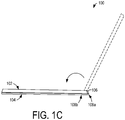
- FIGS. 1A-1C show an example computing system 100 in the form of a tablet having a display 102.
- the computing system is connected to a detachable keyboard unit 104 via a connector 106.
- the keyboard unit 104 comprises a flexible interconnect that electrically connects keys 110 and other electrical components of the keyboard unit 104 to the computing system 100 via the connector 106.
- the keyboard unit 104 and the flexible interconnect positioned therein bend around a bottom corner of the display to a front of the display 102 in a first flex region 108a. As illustrated, the bend in this region is relatively sharp, conforming closely to the corner of the computing system 100.
- the keyboard unit 104 continues up the front surface of the display, and bends sharply down and away from the front surface of the display in a second flex region 108b. The bend in this region is also sharp.
- FIG. 1C shows flex region 108b in a straightened configuration when the computing device 100 and keyboard unit 104 are in a "closed" position, as opposed to an "open” position shown in FIGS. 1A-1B .
- Flex region 108a also may be straightened in a similar manner, for example, when the keyboard unit 104 is removed from the computing device.
- an electronic device that utilizes a flexible interconnect may take any other suitable form.
- the flex regions 108a-b may flex a very large number of cycles during the device lifetime.
- a flexible interconnect having a liquid metal may be used to help prevent loss of conductivity in the event that a solid conductor in the trace is broken from fatigue.
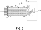
- FIG. 2 shows an example flexible circuit element, in the form of flexible interconnect 200, that may be utilized to provide signal paths in a portion of a device configured to provide a movable or flexible joint, such as the flex regions described above for computing device 100.
- the interconnect 200 includes a plurality of conductive pathways 206 disposed on a flexible substrate 208, and extends between a first electrical component 202 in the form of a connector and a second electrical component 204 in the form of a circuit board having various electronic elements.
- components 202 and 204 may take any suitable form, such as an integrated circuit.
- a longitudinal axis 210 is shown for reference.
- the conductive pathways 206 comprise a liquid metal conductor disposed on the flexible substrate 208.
- Liquid metal can flow to fill the shape of a channel that holds the liquid metal, and therefore is not subject to the fatigue and breakage issues of solid metal traces when repeatedly bent.
- the liquid metal may be used in place of a solid conductor, or may be used in addition to the solid conductor to provide self-healing capabilities for a solid metal trace when the solid metal trace breaks.
- liquid metals may be defined as pure metals or metal alloys with a sufficiently low melting point (Tm) to be in a liquid state at room temperature.
- Non-limiting examples include eutectic gallium/indium (eGaIn), other gallium/indium alloys, eutectic gallium/indium/tin (Galinstan), and other gallium alloys.
- Solid conductors may be defined as electrical conductors having a Tm that is sufficiently above room temperature (e.g., higher than the Tm of liquid metals/conductors), such that the solid metal/conductor is solid at room temperature and at ordinary device operating temperatures.
- the first electrical component 202 and/or the second electrical component 204 may include one or more pins or other interfaces (e.g., pin 212) for coupling to the conductive pathways of the interconnect 200.
- an encapsulant 214 comprising magnetically aligned conductive particles may be formed over at least a portion of the liquid metal conductive pathways 206.
- the encapsulant 214 is positioned at terminal regions of the conductive pathways, such that a middle region of the conductive pathways is not encapsulated by the encapsulant 214 with the magnetically aligned particles, but instead by an encapsulant 216 without such particles.
- the encapsulant 214 comprising the magnetically aligned conductive particles may be formed over the full length of the conductive pathways.
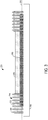
- FIG. 3 shows a sectional view of a portion of the example flexible interconnect 200 of FIG. 2 .
- the substrate 208 may be formed from any suitable electrically insulating, flexible material.
- the substrate 208 is formed from a substantially non-stretchable material, while in other examples a stretchable material may be used, depending upon the device and joint in which the interconnect 200 is to be used.
- suitable materials include, but are not limited to, woven and non-woven fabrics, silicone polymers, flexible plastics, and other polymers (e.g. polyimides, polyethylene terephthalate [PET], polyurethanes, and acrylics).
- a composite substrate may be used, such as a fabric embedded with or coated with a polymer.
- the liquid metal conductor 206 is in contact with the substrate 208, but other layers may be positioned between these layers, such as a solid metal conductive trace layer.
- Any suitable liquid metal may be used that remains in a liquid phase within intended device operating temperature ranges. Examples include, but are not limited to, various alloys of gallium, such as indium/gallium and indium/gallium/tin alloys.
- the liquid metal 206 may be incorporated into the interconnect 200 in any desired manner. For example, an alloy of gallium may be deposited via a needle orifice or the like directly onto the substrate. The outer surface of such an alloy, when exposed to air, forms a thin oxide layer that prevents the liquid metal from spreading, and thus retains the shape in which the liquid metal is initially deposited.
- the encapsulating layer 216 may first be applied over the substrate 208, then a channel formed between the substrate 208 and the encapsulating layer 216, and then the liquid metal introduced into the channel (e.g. by injection or pressure differentials).
- Other example deposition methods include electrochemically depositing the liquid metal from a bath, or spreading the liquid metal onto the solid metal trace, where selective wetting between the liquid metal and the substrate may constrain the shape of the liquid metal.
- the encapsulating layer 216 helps to retain the liquid metal layer in a desired location, and electrically insulates the conductive pathways.
- the encapsulating layer 216 may be formed at least partially from a silicone polymer, a polyimide, or another flexible, non-conductive polymer.
- the encapsulating layer may contact the substrate 208 in regions between conductive pathways 206.
- the encapsulating layer may be deposited in any suitable manner, depending upon the polymer used. For example, a thermoplastic polymer encapsulant may be deposited by heating, spreading over the pathways to be covered (whether prior to or after the addition of the liquid metal), and then cooling.
- a cross-linkable monomer or polymer may be cast onto the substrate and/or conductive pathways to be covered, and then cured.
- a pre-formed encapsulant film may be laminated to the substrate over the conductive pathways. Where the encapsulating layer is added prior to liquid metal inclusion, a channel may be formed at the interface of the substrate and the encapsulating layer after formation of the encapsulating layer, and the liquid metal then may be added to the channel.
- the conductively anisotropic, magnetic particle-embedded encapsulant 214 may include a polymer 302 that is embedded with magnetic particles 304.
- the polymer 302 be formed from the same polymer material as encapsulant 216, or may be utilize one or more different materials.
- the polymer 302 may include an elastomer such as silicone, polyurethane or other members of the urethane family, thermoplastic (e.g., glycopolymer, polystyrene, ethylene butadiene), and/or other materials or composites having elastomeric qualities.
- the magnetic particles 304 may include ferromagnetic particles such as nickel or iron, and/or paramagnetic particles.
- the magnetic particles 304 may include a magnetic core (e.g., iron, nickel, and/or other magnetic material(s) or compound(s)) coated with a conductive material (e.g., comprising copper, gold, silver, and/or other conductive material(s) or compound(s)).
- the particle sizes may range from 50-100 microns in some examples. In other examples, particles of any other suitable size and/or size dispersion may be used.
- a carbon-based filler may be added to the magnetic particle-embedded elastomer to further improve connection robustness.
- Adding carbon-based conductive filler to the magnetic particle-embedded elastomer may reduce the contact resistance at a connection area in systems where low contact resistance is beneficial.
- the carbon-based filler may include carbon black, graphite, carbon nanotube (single wall and/or multi-wall), and graphene, as non-limiting examples.
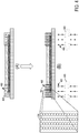
- FIG. 4 illustrates a magnetic particle alignment process.
- the magnetic particles 404 are not aligned and are not in contact with one another. Instead, the magnetic particles are randomly distributed and do not form conductive pathways, as the particle density is too low to be conductive.
- State (B) of FIG. 4 is achieved by the application of a magnetic field 406 to the encapsulant 402.
- the magnetic field 406 may be applied via permanent magnets 408, or electromagnets.
- the application of the magnetic field 406 causes the magnetic particles 404 to align and contact one another to create conductive pathways in a z-direction, as illustrated. While the particles are held in alignment via the magnetic field, the encapsulant may be cured, dried via solvent removal, or otherwise hardened to fix the magnetic particles in the aligned state.
- FIG. 5 shows an example encapsulant hardening process for aligning magnetic particles to control spacing of aligned particles.
- a patterned magnetic shield 502 is positioned between permanent magnet 504 and substrate 506, to provide a plurality of dead zones in which no particles are aligned.
- the particles within the polymer host material will align perpendicular to the substrate, spanning the thickness of the polymer host material.
- the magnetic shield may be omitted, and 'repulsion' of particles along the magnetic field lines may have the effect of aligning the particles along plural, non-intersecting paths through the host material.
- FIG. 6 shows a flow chart illustrating an example method 600 for manufacturing a flexible circuit element.
- Method 600 may be utilized to manufacture interconnects 200 and 300 of FIGS. 2 and 3 , or any other flexible circuit elements.
- method 600 includes depositing a liquid metal conductor to form a conductive path supported by a flexible substrate.
- the term "supported by the substrate” may be used to refer to the liquid metal conductor being either in direct contact with the substrate, or separated from the substrate by one or more intervening layers.
- the liquid metal conductor may be deposited in any suitable manner.
- the liquid metal conductor may be deposited via a syringe in order to form a bead/line of the liquid metal over the flexible substrate.
- the liquid metal conductor may be deposited after formation of an encapsulating layer, for example by forming a microfluidic channel in the encapsulating layer and then introducing the liquid metal into the channel via vacuum or applied pressure.
- a nip roller or doctor bar may be used to pull the liquid metal across the surface of the substrate. The liquid metal may wet the solid traces and thus be deposited on the solid traces, while not wetting the substrate surface.
- the solid traces may be treated with an acid, base, or reducing agent to remove surface oxides prior to liquid metal deposition.
- Other examples of forming the liquid metal layer include electroplating, stencil lithography, evaporation utilizing a shadow mask for patterning, inkjet printing liquid metal in a volatile carrier solvent, and screen printing liquid metal (possibly with additives depending upon the liquid metal used).
- Method 600 further includes, at 604, forming an encapsulating layer to encapsulate the liquid metal and hold the liquid metal in a desired location.
- the encapsulating layer(s) includes a magnetic particle-embedded encapsulant.
- the encapsulating layer may be formed in any suitable manner, including but not limited to via casting, molding and laminating processes.
- multiple layers of liquid metal conductors and encapsulant may be formed to manufacture a multi-layered conductive trace, wherein each layer of encapsulant can act as a substrate for a next solid/liquid metal trace layer.
- the encapsulant may be applied while in a liquid, dissolved, or other viscous state and the embedded magnetic particles are not aligned.
- the magnetic particle-embedded encapsulant may be positioned in terminal regions of the liquid metal conductor, as illustrated at 214 in FIGS. 2 and 3 .
- an encapsulant without magnetic particles may be used to cover a central portion of the liquid metal conductor, as illustrated at 216 in FIGS. 2 and 3 ).
- the different encapsulant regions may be formed in any suitable order, and may be formed from similar or different encapsulant materials.
- the magnetic particle-embedded encapsulant may cover substantially the entire length of the liquid metal conductor, as indicated at 610.
- the encapsulant may be formed (by deposition, magnetic particle alignment, and hardening) prior to application to the substrate, and then laminated onto the substrate.
- method 600 includes applying a magnetic field to align the magnetic particles in the encapsulant.
- the alignment of the magnetic particles may cause the encapsulant to have anisotropic conductivity.
- the conductivity of the encapsulant per unit area or volume may depend on the magnetic field applied during alignment. For example, application of a stronger magnetic field may increase a packing density of the particles of the encapsulant, thereby increasing the density of conductors of the encapsulant, where the encapsulant has sufficient particle loading.
- a patterning mechanism may be used in some examples to form conductive paths with the magnetic particles at desired locations.
- method 600 includes hardening the encapsulant while the magnetic field is applied to hold the magnetic particles in the aligned state.
- the encapsulant may be cured and/or otherwise solidified by any suitable mechanism. Thermal and/or photochemical curing may be employed in some examples.
- a molten thermoplastic host material may be cooled to effect solidification, or volatile solvent may be evaporated.
- the resulting anisotropic conductivity of the encapsulant forms conductive paths extending from the liquid metal conductor.
- Method 600 further comprises, at 618, contacting an external circuit element to the encapsulant having the aligned magnetic particles to connect the external circuit element to the liquid metal conductor.
- the examples disclosed herein may provide increased protection against signal path breakages compared to configurations that use only solid metal traces. Furthermore, the use of a conductively anisotropic, magnetic particle-embedded encapsulant in at least interfacing regions of liquid metal conductive pathways enables conductive pathways to be reliably coupled to rigid or semi-rigid external components and protects against circuit shorting and disconnection during flexing of the liquid metal conductors.
- an interconnect including a substrate, a liquid conductive pathway supported by the substrate, and a conductively anisotropic, magnetic particle-embedded encapsulant that interfaces with the liquid conductive pathway for connecting to another circuit element.
- the magnetic particle-embedded encapsulant may additionally or alternatively be positioned at one or more terminal regions of the liquid conductive pathway, and the interconnect may additionally or alternatively further include an encapsulant that is not embedded with magnetic particles positioned in a central region of the liquid conductive pathway.
- the encapsulant may additionally or alternatively be formed over the full length of the liquid conductive pathway.
- the encapsulant may additionally or alternatively include magnetic particles embedded in an elastomeric polymer.
- the elastomeric polymer may additionally or alternatively include one or more of a silicone, a polyurethane, and a thermoplastic material.
- the magnetic particles may additionally or alternatively include ferromagnetic particles.
- the magnetic particles may additionally or alternatively include paramagnetic particles.
- the magnetic particles may additionally or alternatively include nickel.
- the magnetic particles may additionally or alternatively include magnetic cores coated with a conductor.
- the conductive cores may additionally or alternatively include one or more of gold, silver, and copper. Any or all of the above-described examples may be combined in any suitable manner in various implementations.
- Another example provides for a method of manufacturing an interconnect, the method including depositing a liquid metal conductor to form a conductive path along a flexible substrate, applying an encapsulating layer over at least a portion of the liquid metal conductor, the encapsulating layer including a magnetic particle-embedded encapsulant, applying a magnetic field to the encapsulating layer to align the magnetic particles and cause the magnetic particle-embedded encapsulant to have anisotropic conductivity, and hardening the magnetic particle-embedded encapsulant to hold the magnetic particles in an aligned state.
- the magnetic particle-embedded encapsulant may additionally or alternatively include an elastomeric polymer embedded with the magnetic particles.
- the magnetic particle-embedded encapsulant may additionally or alternatively be applied over at least the portion of the liquid metal conductor while the elastomeric polymer is in a viscous state and the magnetic particles are unaligned.
- applying the encapsulating layer may additionally or alternatively include applying the magnetic particle-embedded encapsulant over terminal regions of the liquid metal conductor and applying an encapsulant that does not include magnetic particles over a central region of the liquid metal conductor.
- the liquid metal conductor may additionally or alternatively be one of a plurality of liquid metal conductors deposited on the flexible substrate forming a plurality of conductive paths.
- applying the encapsulating layer over at least the portion of the liquid metal conductor may additionally or alternatively include applying the encapsulating layer over the plurality of liquid metal conductors such that the encapsulating layer contacts the flexible substrate between adjacent liquid metal conductors.
- a device including a first circuit element, a second circuit element, and an interconnect between the first circuit element and the second circuit element, the interconnect including a liquid conductive pathway, and a conductively anisotropic, magnetic particle-embedded encapsulant that interfaces with the liquid conductive pathway between the liquid conductive pathway and one or more of the first circuit element and the second circuit element.
- the first circuit element and the second element may additionally or alternatively include a printed circuit board or an integrated circuit element.
- the encapsulant may additionally or alternatively include magnetic particles embedded in an elastomeric polymer
- the elastomeric polymer may additionally or alternatively include one or more of a silicone, a polyurethane, and a thermoplastic material
- the magnetic particles may additionally or alternatively include one or more of ferromagnetic particles and ferromagnetic-coated particles.
- the encapsulant may additionally or alternatively further include a carbon-based filler. Any or all of the above-described examples may be combined in any suitable manner in various implementations.
Landscapes
- Engineering & Computer Science (AREA)
- Microelectronics & Electronic Packaging (AREA)
- Manufacturing & Machinery (AREA)
- Combinations Of Printed Boards (AREA)
- Conductive Materials (AREA)
Claims (15)
- Verbindungsvorrichtung (200, 300), umfassend:ein Substrat (208);einen Flüssigkeitsleitpfad, der von dem Substrat getragen wird; undeine leitfähig anisotrope, in magnetische Partikel eingebettete Einkapselung (214, 216, 402), die an den Flüssigkeitsleitpfad anschließt, um eine Verbindung zu einem anderen Schaltungselement herzustellen.
- Verbindungsvorrichtung (200, 300) nach Anspruch 1, wobei die in magnetische Partikel eingebettete Einkapselung (214, 216, 402) an einem oder mehreren Endbereichen des Flüssigkeitsleitpfades positioniert ist, und wobei die Verbindungsvorrichtung ferner eine Einkapselung umfasst, die nicht mit in einem zentralen Bereich des Flüssigkeitsleitpfades positionierten magnetischen Partikeln (304, 404) eingebettet ist.
- Verbindungsvorrichtung (200, 300) nach Anspruch 2, wobei die Einkapselung (214, 216, 402) über die gesamte Länge des Flüssigkeitsleitpfads gebildet wird.
- Verbindungsvorrichtung (200, 300) nach Anspruch 1, wobei die Einkapselung (214, 216, 402) magnetische Partikel (304, 404) enthält, die in ein elastomeres Polymer (302) eingebettet sind.
- Verbindungsvorrichtung (200, 300) nach Anspruch 4, wobei das elastomere Polymer (302) ein oder mehrere aus einem Silikon, einem Polyurethan und einem thermoplastischen Material enthält.
- Verbindungsvorrichtung (200, 300) nach Anspruch 4, wobei die magnetischen Partikel (304, 404) ferromagnetische Partikel enthalten.
- Verbindungsvorrichtung (200, 300) nach Anspruch 4, wobei die magnetischen Partikel (304, 404) paramagnetische Partikel enthalten.
- Verbindungsvorrichtung (200, 300) nach Anspruch 4, wobei die magnetischen Partikel (304, 404) Magnetkerne enthalten, die mit einem Leiter beschichtet sind.
- Verbindungsvorrichtung (200, 300) nach Anspruch 8, wobei die leitenden Kerne einen oder mehrere aus Gold, Silber und Kupfer enthalten.
- Verfahren (600) zur Herstellung einer Verbindungsvorrichtung (200, 300), wobei das Verfahren umfasst:Aufbringen eines Flüssigmetall-Leiters (206), um einen leitenden Pfad entlang eines flexiblen Substrats (208) zu bilden;Auftragen einer Einkapselungsschicht (216) über mindestens einen Bereich des Flüssigmetall-Leiters, wobei die Einkapselungsschicht eine in magnetische Partikel eingebettete Einkapselung (214, 216, 402) enthält;Anwenden eines Magnetfeldes (406) auf die Einkapselungsschicht, um die magnetischen Partikel (304, 404) auszurichten und zu bewirken, dass die in magnetische Partikel eingebettete Einkapselung eine anisotrope Leitfähigkeit aufweist; undHärten der in magnetische Partikel eingebetteten Einkapselung, um die magnetischen Partikel in einem ausgerichteten Zustand zu halten.
- Verfahren (600) nach Anspruch 10, wobei die in magnetische Partikel eingebettete Einkapselung (214, 216, 402) ein elastomeres Polymer (302) umfasst, das in die magnetischen Partikel (304, 404) eingebettet ist.
- Verfahren (600) nach Anspruch 11, bei dem die in magnetische Partikel eingebettete Einkapselung (214, 216, 402) über mindestens den Bereich des Flüssigmetall-Leiters (206) aufgetragen wird, während sich das elastomere Polymer (302) in einem viskosen Zustand befindet und die magnetischen Partikel (304, 404) unausgerichtet sind.
- Verfahren (600) nach Anspruch 10, wobei das Auftragen der Einkapselungsschicht (216) das Auftragen der in magnetische Partikel eingebetteten Einkapselung (214, 216, 402) über Endbereiche des Flüssigmetall-Leiters (206) und das Auftragen einer Einkapselung, die über einem zentralen Bereich des Flüssigmetall-Leiters keine magnetischen Partikel (304, 404) enthält.
- Verfahren (600) nach Anspruch 10, wobei der Flüssigmetall-Leiter (206) einer von mehreren Flüssigmetall-Leitern (206) ist, die auf einem flexiblen Substrat (208) aufgetragen sind und mehrere Leiterbahnen bilden.
- Verfahren (600) nach Anspruch 14, wobei das Auftragen der Einkapselungsschicht (216) über mindestens den Bereich des Flüssigmetall-Leiters (206) das Auftragen der Einkapselungsschicht über die Vielzahl von Flüssigmetall-Leitern (206) enthält, so dass die Einkapselungsschicht das flexible Substrat (208) zwischen benachbarten Flüssigmetall-Leitern berührt.
Applications Claiming Priority (2)
| Application Number | Priority Date | Filing Date | Title |
|---|---|---|---|
| US15/239,645 US9872390B1 (en) | 2016-08-17 | 2016-08-17 | Flexible interconnect |
| PCT/US2017/046180 WO2018034914A1 (en) | 2016-08-17 | 2017-08-10 | Flexible interconnect |
Publications (2)
| Publication Number | Publication Date |
|---|---|
| EP3501043A1 EP3501043A1 (de) | 2019-06-26 |
| EP3501043B1 true EP3501043B1 (de) | 2020-10-14 |
Family
ID=59746346
Family Applications (1)
| Application Number | Title | Priority Date | Filing Date |
|---|---|---|---|
| EP17761147.2A Active EP3501043B1 (de) | 2016-08-17 | 2017-08-10 | Flexible verbindung |
Country Status (4)
| Country | Link |
|---|---|
| US (1) | US9872390B1 (de) |
| EP (1) | EP3501043B1 (de) |
| CN (1) | CN109643696B (de) |
| WO (1) | WO2018034914A1 (de) |
Families Citing this family (11)
| Publication number | Priority date | Publication date | Assignee | Title |
|---|---|---|---|---|
| US10327332B2 (en) * | 2016-10-06 | 2019-06-18 | Microsoft Technology Licensing, Llc | Connecting a flexible circuit to other structures |
| US10757815B2 (en) * | 2018-01-09 | 2020-08-25 | Carnegie Mellon University | Method for fabrication of a soft-matter printed circuit board |
| US11503720B2 (en) | 2018-09-17 | 2022-11-15 | 3M Innovative Properties Company | Flexible device including conductive traces with enhanced stretchability |
| US10879151B2 (en) * | 2018-12-28 | 2020-12-29 | Texas Instruments Incorporated | Semiconductor package with liquid metal conductors |
| US11805597B2 (en) * | 2019-03-12 | 2023-10-31 | Carnegie Mellon University | Liquid metal circuits and methods of making the same |
| TWI749564B (zh) * | 2020-05-25 | 2021-12-11 | 奇翼醫電股份有限公司 | 導電凸點電極結構 |
| CN115413184A (zh) * | 2021-05-29 | 2022-11-29 | 华为技术有限公司 | 一种散热系统和电子设备 |
| CN114843067B (zh) * | 2022-04-18 | 2023-06-23 | 电子科技大学 | 一种柔性电感及其制备方法 |
| CN116583009A (zh) * | 2023-06-30 | 2023-08-11 | 西安交通大学 | 一种抗弯折铜基自愈合双层电路及其高精度制造工艺 |
| CN119342682A (zh) * | 2023-07-20 | 2025-01-21 | 宏启胜精密电子(秦皇岛)有限公司 | 软性电路板及其制造方法 |
| CN118973081A (zh) * | 2024-08-20 | 2024-11-15 | 深圳有泽芯材科技有限公司 | 一种具备自修复功能的智能柔性线路板 |
Family Cites Families (11)
| Publication number | Priority date | Publication date | Assignee | Title |
|---|---|---|---|---|
| US5757615A (en) * | 1996-07-01 | 1998-05-26 | Compaq Computer Corporation | Liquid cooled computer apparatus and associated methods |
| US6190509B1 (en) * | 1997-03-04 | 2001-02-20 | Tessera, Inc. | Methods of making anisotropic conductive elements for use in microelectronic packaging |
| US20020086566A1 (en) * | 2000-12-06 | 2002-07-04 | Simons Everett F. | Robust, low-resistance elastomeric conductive polymer interconnect |
| ATE515078T1 (de) * | 2003-01-17 | 2011-07-15 | Jsr Corp | Anisotroper leitfähiger verbinder und herstellungsverfahren dafür und untersuchungseinheit für eine schaltungseinrichtung |
| JP2008546542A (ja) * | 2005-05-18 | 2008-12-25 | プレジデント・アンド・フエローズ・オブ・ハーバード・カレツジ | マイクロ流体ネットワークにおける伝導通路、マイクロ回路、マイクロ構造の製造 |
| JP4955970B2 (ja) * | 2005-09-20 | 2012-06-20 | 住友電気工業株式会社 | フレキシブルプリント配線板およびその製造方法 |
| CN101505575B (zh) * | 2008-12-26 | 2011-01-19 | 深圳大学 | 一种基于pdms生物可兼容性的柔性电路的制作方法 |
| US9116145B2 (en) | 2011-12-14 | 2015-08-25 | The George Washington University | Flexible IC/microfluidic integration and packaging |
| CN104445055B (zh) | 2014-12-01 | 2016-01-13 | 华中科技大学 | 一种可提高延展性的柔性电子流体封装方法 |
| US10945339B2 (en) * | 2015-02-09 | 2021-03-09 | Carnegie Mellon University | High-density soft-matter electronics |
| CN105845204A (zh) * | 2016-04-12 | 2016-08-10 | 京东方科技集团股份有限公司 | 各向异性导电胶、显示装置及基板与外接电路的邦定方法 |
-
2016
- 2016-08-17 US US15/239,645 patent/US9872390B1/en active Active
-
2017
- 2017-08-10 WO PCT/US2017/046180 patent/WO2018034914A1/en not_active Ceased
- 2017-08-10 CN CN201780050502.7A patent/CN109643696B/zh active Active
- 2017-08-10 EP EP17761147.2A patent/EP3501043B1/de active Active
Non-Patent Citations (1)
| Title |
|---|
| None * |
Also Published As
| Publication number | Publication date |
|---|---|
| US9872390B1 (en) | 2018-01-16 |
| WO2018034914A1 (en) | 2018-02-22 |
| EP3501043A1 (de) | 2019-06-26 |
| CN109643696A (zh) | 2019-04-16 |
| CN109643696B (zh) | 2023-06-27 |
Similar Documents
| Publication | Publication Date | Title |
|---|---|---|
| EP3501043B1 (de) | Flexible verbindung | |
| CN109417850B (zh) | 柔性互连 | |
| US9983229B2 (en) | Test socket for testing semiconductor chip package and method of manufacturing the same | |
| US9536815B2 (en) | Semiconductor socket with direct selective metalization | |
| CN112203410A (zh) | 埋入式电路板及其制备方法 | |
| US20120051016A1 (en) | Semiconductor socket | |
| US20150136467A1 (en) | High speed circuit assembly with integral terminal and mating bias loading electrical connector assembly | |
| KR20150134773A (ko) | 신축성 전극 및 이의 제조방법 | |
| US11219124B2 (en) | Connecting a flexible circuit to other structures | |
| EP3564991B1 (de) | Verfahren zur herstellung eines elektronischen moduls | |
| US11877386B2 (en) | Injection molded article and method for producing same | |
| US8093712B2 (en) | Monolithic molded flexible electronic assemblies without solder and methods for their manufacture | |
| JP4085518B2 (ja) | 金型およびその製造方法、金型製造用鋳型並びに異方導電性シートの製造方法 | |
| JP3903662B2 (ja) | 異方導電性シートおよびその製造方法 | |
| JP2009054304A (ja) | 異方導電性コネクタ | |
| US20180375239A1 (en) | Liquid metal circuit element connector | |
| JP2019036394A (ja) | 異方導電性シートおよび異方導電性シートの製造方法 | |
| US20130146343A1 (en) | Printed circuit board and method of manufacturing the same | |
| JP2008205381A (ja) | 半導体装置 | |
| JP2001084841A (ja) | 異方導電性シートおよびその製造方法 | |
| JP2000238046A (ja) | 異方導電性シート製造用金型、その製造方法及び異方導電性シート製造装置 | |
| JP2003059978A (ja) | 電子部品実装用フィルムキャリアテープの製造方法及び製造装置 | |
| JPH0365636B2 (de) |
Legal Events
| Date | Code | Title | Description |
|---|---|---|---|
| STAA | Information on the status of an ep patent application or granted ep patent |
Free format text: STATUS: UNKNOWN |
|
| STAA | Information on the status of an ep patent application or granted ep patent |
Free format text: STATUS: THE INTERNATIONAL PUBLICATION HAS BEEN MADE |
|
| PUAI | Public reference made under article 153(3) epc to a published international application that has entered the european phase |
Free format text: ORIGINAL CODE: 0009012 |
|
| STAA | Information on the status of an ep patent application or granted ep patent |
Free format text: STATUS: REQUEST FOR EXAMINATION WAS MADE |
|
| 17P | Request for examination filed |
Effective date: 20190214 |
|
| AK | Designated contracting states |
Kind code of ref document: A1 Designated state(s): AL AT BE BG CH CY CZ DE DK EE ES FI FR GB GR HR HU IE IS IT LI LT LU LV MC MK MT NL NO PL PT RO RS SE SI SK SM TR |
|
| AX | Request for extension of the european patent |
Extension state: BA ME |
|
| DAV | Request for validation of the european patent (deleted) | ||
| DAX | Request for extension of the european patent (deleted) | ||
| GRAP | Despatch of communication of intention to grant a patent |
Free format text: ORIGINAL CODE: EPIDOSNIGR1 |
|
| STAA | Information on the status of an ep patent application or granted ep patent |
Free format text: STATUS: GRANT OF PATENT IS INTENDED |
|
| INTG | Intention to grant announced |
Effective date: 20200507 |
|
| GRAS | Grant fee paid |
Free format text: ORIGINAL CODE: EPIDOSNIGR3 |
|
| GRAA | (expected) grant |
Free format text: ORIGINAL CODE: 0009210 |
|
| STAA | Information on the status of an ep patent application or granted ep patent |
Free format text: STATUS: THE PATENT HAS BEEN GRANTED |
|
| AK | Designated contracting states |
Kind code of ref document: B1 Designated state(s): AL AT BE BG CH CY CZ DE DK EE ES FI FR GB GR HR HU IE IS IT LI LT LU LV MC MK MT NL NO PL PT RO RS SE SI SK SM TR |
|
| REG | Reference to a national code |
Ref country code: GB Ref legal event code: FG4D |
|
| REG | Reference to a national code |
Ref country code: AT Ref legal event code: REF Ref document number: 1324414 Country of ref document: AT Kind code of ref document: T Effective date: 20201015 Ref country code: CH Ref legal event code: EP |
|
| REG | Reference to a national code |
Ref country code: DE Ref legal event code: R096 Ref document number: 602017025539 Country of ref document: DE |
|
| REG | Reference to a national code |
Ref country code: IE Ref legal event code: FG4D |
|
| REG | Reference to a national code |
Ref country code: AT Ref legal event code: MK05 Ref document number: 1324414 Country of ref document: AT Kind code of ref document: T Effective date: 20201014 |
|
| REG | Reference to a national code |
Ref country code: NL Ref legal event code: MP Effective date: 20201014 |
|
| PG25 | Lapsed in a contracting state [announced via postgrant information from national office to epo] |
Ref country code: FI Free format text: LAPSE BECAUSE OF FAILURE TO SUBMIT A TRANSLATION OF THE DESCRIPTION OR TO PAY THE FEE WITHIN THE PRESCRIBED TIME-LIMIT Effective date: 20201014 Ref country code: GR Free format text: LAPSE BECAUSE OF FAILURE TO SUBMIT A TRANSLATION OF THE DESCRIPTION OR TO PAY THE FEE WITHIN THE PRESCRIBED TIME-LIMIT Effective date: 20210115 Ref country code: NO Free format text: LAPSE BECAUSE OF FAILURE TO SUBMIT A TRANSLATION OF THE DESCRIPTION OR TO PAY THE FEE WITHIN THE PRESCRIBED TIME-LIMIT Effective date: 20210114 Ref country code: RS Free format text: LAPSE BECAUSE OF FAILURE TO SUBMIT A TRANSLATION OF THE DESCRIPTION OR TO PAY THE FEE WITHIN THE PRESCRIBED TIME-LIMIT Effective date: 20201014 Ref country code: PT Free format text: LAPSE BECAUSE OF FAILURE TO SUBMIT A TRANSLATION OF THE DESCRIPTION OR TO PAY THE FEE WITHIN THE PRESCRIBED TIME-LIMIT Effective date: 20210215 |
|
| REG | Reference to a national code |
Ref country code: LT Ref legal event code: MG4D |
|
| PG25 | Lapsed in a contracting state [announced via postgrant information from national office to epo] |
Ref country code: ES Free format text: LAPSE BECAUSE OF FAILURE TO SUBMIT A TRANSLATION OF THE DESCRIPTION OR TO PAY THE FEE WITHIN THE PRESCRIBED TIME-LIMIT Effective date: 20201014 Ref country code: AT Free format text: LAPSE BECAUSE OF FAILURE TO SUBMIT A TRANSLATION OF THE DESCRIPTION OR TO PAY THE FEE WITHIN THE PRESCRIBED TIME-LIMIT Effective date: 20201014 Ref country code: BG Free format text: LAPSE BECAUSE OF FAILURE TO SUBMIT A TRANSLATION OF THE DESCRIPTION OR TO PAY THE FEE WITHIN THE PRESCRIBED TIME-LIMIT Effective date: 20210114 Ref country code: PL Free format text: LAPSE BECAUSE OF FAILURE TO SUBMIT A TRANSLATION OF THE DESCRIPTION OR TO PAY THE FEE WITHIN THE PRESCRIBED TIME-LIMIT Effective date: 20201014 Ref country code: IS Free format text: LAPSE BECAUSE OF FAILURE TO SUBMIT A TRANSLATION OF THE DESCRIPTION OR TO PAY THE FEE WITHIN THE PRESCRIBED TIME-LIMIT Effective date: 20210214 Ref country code: LV Free format text: LAPSE BECAUSE OF FAILURE TO SUBMIT A TRANSLATION OF THE DESCRIPTION OR TO PAY THE FEE WITHIN THE PRESCRIBED TIME-LIMIT Effective date: 20201014 Ref country code: SE Free format text: LAPSE BECAUSE OF FAILURE TO SUBMIT A TRANSLATION OF THE DESCRIPTION OR TO PAY THE FEE WITHIN THE PRESCRIBED TIME-LIMIT Effective date: 20201014 |
|
| PG25 | Lapsed in a contracting state [announced via postgrant information from national office to epo] |
Ref country code: HR Free format text: LAPSE BECAUSE OF FAILURE TO SUBMIT A TRANSLATION OF THE DESCRIPTION OR TO PAY THE FEE WITHIN THE PRESCRIBED TIME-LIMIT Effective date: 20201014 Ref country code: NL Free format text: LAPSE BECAUSE OF FAILURE TO SUBMIT A TRANSLATION OF THE DESCRIPTION OR TO PAY THE FEE WITHIN THE PRESCRIBED TIME-LIMIT Effective date: 20201014 |
|
| REG | Reference to a national code |
Ref country code: DE Ref legal event code: R097 Ref document number: 602017025539 Country of ref document: DE |
|
| PG25 | Lapsed in a contracting state [announced via postgrant information from national office to epo] |
Ref country code: SK Free format text: LAPSE BECAUSE OF FAILURE TO SUBMIT A TRANSLATION OF THE DESCRIPTION OR TO PAY THE FEE WITHIN THE PRESCRIBED TIME-LIMIT Effective date: 20201014 Ref country code: RO Free format text: LAPSE BECAUSE OF FAILURE TO SUBMIT A TRANSLATION OF THE DESCRIPTION OR TO PAY THE FEE WITHIN THE PRESCRIBED TIME-LIMIT Effective date: 20201014 Ref country code: SM Free format text: LAPSE BECAUSE OF FAILURE TO SUBMIT A TRANSLATION OF THE DESCRIPTION OR TO PAY THE FEE WITHIN THE PRESCRIBED TIME-LIMIT Effective date: 20201014 Ref country code: EE Free format text: LAPSE BECAUSE OF FAILURE TO SUBMIT A TRANSLATION OF THE DESCRIPTION OR TO PAY THE FEE WITHIN THE PRESCRIBED TIME-LIMIT Effective date: 20201014 Ref country code: CZ Free format text: LAPSE BECAUSE OF FAILURE TO SUBMIT A TRANSLATION OF THE DESCRIPTION OR TO PAY THE FEE WITHIN THE PRESCRIBED TIME-LIMIT Effective date: 20201014 Ref country code: LT Free format text: LAPSE BECAUSE OF FAILURE TO SUBMIT A TRANSLATION OF THE DESCRIPTION OR TO PAY THE FEE WITHIN THE PRESCRIBED TIME-LIMIT Effective date: 20201014 |
|
| PLBE | No opposition filed within time limit |
Free format text: ORIGINAL CODE: 0009261 |
|
| STAA | Information on the status of an ep patent application or granted ep patent |
Free format text: STATUS: NO OPPOSITION FILED WITHIN TIME LIMIT |
|
| PG25 | Lapsed in a contracting state [announced via postgrant information from national office to epo] |
Ref country code: DK Free format text: LAPSE BECAUSE OF FAILURE TO SUBMIT A TRANSLATION OF THE DESCRIPTION OR TO PAY THE FEE WITHIN THE PRESCRIBED TIME-LIMIT Effective date: 20201014 |
|
| 26N | No opposition filed |
Effective date: 20210715 |
|
| PG25 | Lapsed in a contracting state [announced via postgrant information from national office to epo] |
Ref country code: IT Free format text: LAPSE BECAUSE OF FAILURE TO SUBMIT A TRANSLATION OF THE DESCRIPTION OR TO PAY THE FEE WITHIN THE PRESCRIBED TIME-LIMIT Effective date: 20201014 Ref country code: AL Free format text: LAPSE BECAUSE OF FAILURE TO SUBMIT A TRANSLATION OF THE DESCRIPTION OR TO PAY THE FEE WITHIN THE PRESCRIBED TIME-LIMIT Effective date: 20201014 |
|
| PG25 | Lapsed in a contracting state [announced via postgrant information from national office to epo] |
Ref country code: SI Free format text: LAPSE BECAUSE OF FAILURE TO SUBMIT A TRANSLATION OF THE DESCRIPTION OR TO PAY THE FEE WITHIN THE PRESCRIBED TIME-LIMIT Effective date: 20201014 |
|
| REG | Reference to a national code |
Ref country code: CH Ref legal event code: PL |
|
| PG25 | Lapsed in a contracting state [announced via postgrant information from national office to epo] |
Ref country code: MC Free format text: LAPSE BECAUSE OF FAILURE TO SUBMIT A TRANSLATION OF THE DESCRIPTION OR TO PAY THE FEE WITHIN THE PRESCRIBED TIME-LIMIT Effective date: 20201014 |
|
| REG | Reference to a national code |
Ref country code: BE Ref legal event code: MM Effective date: 20210831 |
|
| PG25 | Lapsed in a contracting state [announced via postgrant information from national office to epo] |
Ref country code: LI Free format text: LAPSE BECAUSE OF NON-PAYMENT OF DUE FEES Effective date: 20210831 Ref country code: CH Free format text: LAPSE BECAUSE OF NON-PAYMENT OF DUE FEES Effective date: 20210831 |
|
| PG25 | Lapsed in a contracting state [announced via postgrant information from national office to epo] |
Ref country code: IS Free format text: LAPSE BECAUSE OF FAILURE TO SUBMIT A TRANSLATION OF THE DESCRIPTION OR TO PAY THE FEE WITHIN THE PRESCRIBED TIME-LIMIT Effective date: 20210214 Ref country code: LU Free format text: LAPSE BECAUSE OF NON-PAYMENT OF DUE FEES Effective date: 20210810 |
|
| PG25 | Lapsed in a contracting state [announced via postgrant information from national office to epo] |
Ref country code: IE Free format text: LAPSE BECAUSE OF NON-PAYMENT OF DUE FEES Effective date: 20210810 Ref country code: BE Free format text: LAPSE BECAUSE OF NON-PAYMENT OF DUE FEES Effective date: 20210831 |
|
| P01 | Opt-out of the competence of the unified patent court (upc) registered |
Effective date: 20230512 |
|
| PG25 | Lapsed in a contracting state [announced via postgrant information from national office to epo] |
Ref country code: CY Free format text: LAPSE BECAUSE OF FAILURE TO SUBMIT A TRANSLATION OF THE DESCRIPTION OR TO PAY THE FEE WITHIN THE PRESCRIBED TIME-LIMIT Effective date: 20201014 |
|
| PG25 | Lapsed in a contracting state [announced via postgrant information from national office to epo] |
Ref country code: HU Free format text: LAPSE BECAUSE OF FAILURE TO SUBMIT A TRANSLATION OF THE DESCRIPTION OR TO PAY THE FEE WITHIN THE PRESCRIBED TIME-LIMIT; INVALID AB INITIO Effective date: 20170810 |
|
| PG25 | Lapsed in a contracting state [announced via postgrant information from national office to epo] |
Ref country code: MK Free format text: LAPSE BECAUSE OF FAILURE TO SUBMIT A TRANSLATION OF THE DESCRIPTION OR TO PAY THE FEE WITHIN THE PRESCRIBED TIME-LIMIT Effective date: 20201014 |
|
| PG25 | Lapsed in a contracting state [announced via postgrant information from national office to epo] |
Ref country code: TR Free format text: LAPSE BECAUSE OF FAILURE TO SUBMIT A TRANSLATION OF THE DESCRIPTION OR TO PAY THE FEE WITHIN THE PRESCRIBED TIME-LIMIT Effective date: 20201014 |
|
| PG25 | Lapsed in a contracting state [announced via postgrant information from national office to epo] |
Ref country code: MT Free format text: LAPSE BECAUSE OF FAILURE TO SUBMIT A TRANSLATION OF THE DESCRIPTION OR TO PAY THE FEE WITHIN THE PRESCRIBED TIME-LIMIT Effective date: 20201014 |
|
| PGFP | Annual fee paid to national office [announced via postgrant information from national office to epo] |
Ref country code: DE Payment date: 20250724 Year of fee payment: 9 |
|
| PGFP | Annual fee paid to national office [announced via postgrant information from national office to epo] |
Ref country code: GB Payment date: 20250724 Year of fee payment: 9 |
|
| PGFP | Annual fee paid to national office [announced via postgrant information from national office to epo] |
Ref country code: FR Payment date: 20250725 Year of fee payment: 9 |
|
| REG | Reference to a national code |
Ref country code: DE Ref legal event code: R079 Ref document number: 602017025539 Country of ref document: DE Free format text: PREVIOUS MAIN CLASS: H01L0023498000 Ipc: H10W0070620000 |