EP3499651B1 - Connector - Google Patents
Connector Download PDFInfo
- Publication number
- EP3499651B1 EP3499651B1 EP17839586.9A EP17839586A EP3499651B1 EP 3499651 B1 EP3499651 B1 EP 3499651B1 EP 17839586 A EP17839586 A EP 17839586A EP 3499651 B1 EP3499651 B1 EP 3499651B1
- Authority
- EP
- European Patent Office
- Prior art keywords
- connector
- insulator
- fitting
- fixing
- movable
- Prior art date
- Legal status (The legal status is an assumption and is not a legal conclusion. Google has not performed a legal analysis and makes no representation as to the accuracy of the status listed.)
- Active
Links
Images


Classifications
-
- H—ELECTRICITY
- H01—ELECTRIC ELEMENTS
- H01R—ELECTRICALLY-CONDUCTIVE CONNECTIONS; STRUCTURAL ASSOCIATIONS OF A PLURALITY OF MUTUALLY-INSULATED ELECTRICAL CONNECTING ELEMENTS; COUPLING DEVICES; CURRENT COLLECTORS
- H01R13/00—Details of coupling devices of the kinds covered by groups H01R12/70 or H01R24/00 - H01R33/00
- H01R13/40—Securing contact members in or to a base or case; Insulating of contact members
-
- H—ELECTRICITY
- H01—ELECTRIC ELEMENTS
- H01R—ELECTRICALLY-CONDUCTIVE CONNECTIONS; STRUCTURAL ASSOCIATIONS OF A PLURALITY OF MUTUALLY-INSULATED ELECTRICAL CONNECTING ELEMENTS; COUPLING DEVICES; CURRENT COLLECTORS
- H01R12/00—Structural associations of a plurality of mutually-insulated electrical connecting elements, specially adapted for printed circuits, e.g. printed circuit boards [PCB], flat or ribbon cables, or like generally planar structures, e.g. terminal strips, terminal blocks; Coupling devices specially adapted for printed circuits, flat or ribbon cables, or like generally planar structures; Terminals specially adapted for contact with, or insertion into, printed circuits, flat or ribbon cables, or like generally planar structures
- H01R12/70—Coupling devices
- H01R12/71—Coupling devices for rigid printing circuits or like structures
- H01R12/72—Coupling devices for rigid printing circuits or like structures coupling with the edge of the rigid printed circuits or like structures
- H01R12/721—Coupling devices for rigid printing circuits or like structures coupling with the edge of the rigid printed circuits or like structures cooperating directly with the edge of the rigid printed circuits
-
- H—ELECTRICITY
- H01—ELECTRIC ELEMENTS
- H01R—ELECTRICALLY-CONDUCTIVE CONNECTIONS; STRUCTURAL ASSOCIATIONS OF A PLURALITY OF MUTUALLY-INSULATED ELECTRICAL CONNECTING ELEMENTS; COUPLING DEVICES; CURRENT COLLECTORS
- H01R12/00—Structural associations of a plurality of mutually-insulated electrical connecting elements, specially adapted for printed circuits, e.g. printed circuit boards [PCB], flat or ribbon cables, or like generally planar structures, e.g. terminal strips, terminal blocks; Coupling devices specially adapted for printed circuits, flat or ribbon cables, or like generally planar structures; Terminals specially adapted for contact with, or insertion into, printed circuits, flat or ribbon cables, or like generally planar structures
- H01R12/70—Coupling devices
- H01R12/71—Coupling devices for rigid printing circuits or like structures
- H01R12/72—Coupling devices for rigid printing circuits or like structures coupling with the edge of the rigid printed circuits or like structures
- H01R12/73—Coupling devices for rigid printing circuits or like structures coupling with the edge of the rigid printed circuits or like structures connecting to other rigid printed circuits or like structures
-
- H—ELECTRICITY
- H01—ELECTRIC ELEMENTS
- H01R—ELECTRICALLY-CONDUCTIVE CONNECTIONS; STRUCTURAL ASSOCIATIONS OF A PLURALITY OF MUTUALLY-INSULATED ELECTRICAL CONNECTING ELEMENTS; COUPLING DEVICES; CURRENT COLLECTORS
- H01R12/00—Structural associations of a plurality of mutually-insulated electrical connecting elements, specially adapted for printed circuits, e.g. printed circuit boards [PCB], flat or ribbon cables, or like generally planar structures, e.g. terminal strips, terminal blocks; Coupling devices specially adapted for printed circuits, flat or ribbon cables, or like generally planar structures; Terminals specially adapted for contact with, or insertion into, printed circuits, flat or ribbon cables, or like generally planar structures
- H01R12/70—Coupling devices
- H01R12/91—Coupling devices allowing relative movement between coupling parts, e.g. floating or self aligning
-
- H—ELECTRICITY
- H01—ELECTRIC ELEMENTS
- H01R—ELECTRICALLY-CONDUCTIVE CONNECTIONS; STRUCTURAL ASSOCIATIONS OF A PLURALITY OF MUTUALLY-INSULATED ELECTRICAL CONNECTING ELEMENTS; COUPLING DEVICES; CURRENT COLLECTORS
- H01R13/00—Details of coupling devices of the kinds covered by groups H01R12/70 or H01R24/00 - H01R33/00
- H01R13/62—Means for facilitating engagement or disengagement of coupling parts or for holding them in engagement
- H01R13/629—Additional means for facilitating engagement or disengagement of coupling parts, e.g. aligning or guiding means, levers, gas pressure electrical locking indicators, manufacturing tolerances
- H01R13/631—Additional means for facilitating engagement or disengagement of coupling parts, e.g. aligning or guiding means, levers, gas pressure electrical locking indicators, manufacturing tolerances for engagement only
-
- H—ELECTRICITY
- H01—ELECTRIC ELEMENTS
- H01R—ELECTRICALLY-CONDUCTIVE CONNECTIONS; STRUCTURAL ASSOCIATIONS OF A PLURALITY OF MUTUALLY-INSULATED ELECTRICAL CONNECTING ELEMENTS; COUPLING DEVICES; CURRENT COLLECTORS
- H01R12/00—Structural associations of a plurality of mutually-insulated electrical connecting elements, specially adapted for printed circuits, e.g. printed circuit boards [PCB], flat or ribbon cables, or like generally planar structures, e.g. terminal strips, terminal blocks; Coupling devices specially adapted for printed circuits, flat or ribbon cables, or like generally planar structures; Terminals specially adapted for contact with, or insertion into, printed circuits, flat or ribbon cables, or like generally planar structures
- H01R12/70—Coupling devices
- H01R12/7005—Guiding, mounting, polarizing or locking means; Extractors
- H01R12/7011—Locking or fixing a connector to a PCB
- H01R12/707—Soldering or welding
-
- H—ELECTRICITY
- H01—ELECTRIC ELEMENTS
- H01R—ELECTRICALLY-CONDUCTIVE CONNECTIONS; STRUCTURAL ASSOCIATIONS OF A PLURALITY OF MUTUALLY-INSULATED ELECTRICAL CONNECTING ELEMENTS; COUPLING DEVICES; CURRENT COLLECTORS
- H01R12/00—Structural associations of a plurality of mutually-insulated electrical connecting elements, specially adapted for printed circuits, e.g. printed circuit boards [PCB], flat or ribbon cables, or like generally planar structures, e.g. terminal strips, terminal blocks; Coupling devices specially adapted for printed circuits, flat or ribbon cables, or like generally planar structures; Terminals specially adapted for contact with, or insertion into, printed circuits, flat or ribbon cables, or like generally planar structures
- H01R12/70—Coupling devices
- H01R12/71—Coupling devices for rigid printing circuits or like structures
- H01R12/72—Coupling devices for rigid printing circuits or like structures coupling with the edge of the rigid printed circuits or like structures
- H01R12/73—Coupling devices for rigid printing circuits or like structures coupling with the edge of the rigid printed circuits or like structures connecting to other rigid printed circuits or like structures
- H01R12/735—Printed circuits including an angle between each other
- H01R12/737—Printed circuits being substantially perpendicular to each other
Definitions
- the present invention relates to a connector.
- Connectors connecting different substrates are known.
- This type of connector is configured such that a first connector attached to one substrate is fitted to a second connector attached to the other substrate.
- the first connector includes: a fixing insulator fixed to a substrate surface of one substrate; a movable insulator that is disposed to be movable relative to the fixing insulator; and a plurality of contacts that are mounted on the one substrate, that are held by the fixing insulator and the movable insulator, and that are arranged alongside in one direction.
- Each of the contacts includes an elastic deformation portion that can be elastically deformed.
- elastic deformation of the elastic deformation portion allows the movable insulator to move relative to the fixing insulator. This can absorb positional deviation when the second connector is fitted to the first connector and allows positional deviation after the fitting.
- Part of the movable insulator is disposed between the fixing insulator and the substrate surface. This allows the movable insulator to be fitted to the fixing insulator when the second connector is removed from the first connector, whereby the movement of the movable insulator toward the second connector is restricted.
- Patent Document 1 Japanese Laid-open Patent Publication No. 2014-67706
- Size reduction has been demanded for the above-described connector, including reduction in the occupied area of the connector mounted on the substrate.
- size reduction in the fixing insulator and the movable insulator there is a limitation on size reduction in a contact array direction in which a plurality of contacts is arrayed because the number of contacts is fixed.
- size reduction in a width direction orthogonal to the contact array direction is conceivable.
- the size reduction in the width direction causes decrease in strength. For this reason, there is a possibility of the fixing insulator or the like being damaged when, for example, the second connector is removed from the first connector or unintentional force is applied.
- a connector has a movable insulator, both ends in a contact array direction of which face metal fittings.
- the metal fittings restrict the movement of the movable insulator in a fitting direction.
- the connector is provided in a state where the metal fittings are disposed inside the fixing insulator, i.e., in a state where the metal fittings are not exposed on the surface at the fitting side of the fixing insulator.
- the connector may reduce its size, prevent decrease in strength, and improve fitting performance when the other connector is fitted to the connector.
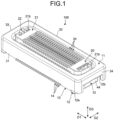
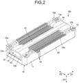
- FIG. 1 and FIG. 2 are perspective views each illustrating an example of a connector 100 according to embodiments.
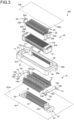
- FIG. 3 is an exploded perspective view illustrating a configuration of the connector 100.
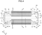
- FIG. 4 is a bottom view illustrating an example of the connector 100 when viewed from a first substrate 101 side.
- the connector 100 includes a first connector (connector) 10 and a second connector (another/the other connector) 20.
- FIG. 1 , FIG. 2 , and FIG. 4 each illustrate a state where the first connector 10 and the second connector 20 are fitted to each other. While embodiments refer to the connector as being configured to include the first connector 10 and the second connector 20, each of the first connector 10 and the second connector 20 is actually configured as a single connector.
- FIG. 1 and FIG. 2 are perspective views each illustrating an example of a connector 100 according to embodiments.
- FIG. 3 is an exploded perspective view illustrating a configuration of the connector 100.
- FIG. 4 is a bottom view illustrating an example of the connector 100 when viewed from
- FIG. 5 is a diagram illustrating an example of the first connector 10.
- FIG. 5 illustrates the first connector 10 when viewed from a fitting surface side of the first connector 10, the fitting surface being fitted to the second connector 20.
- FIG. 6 is a diagram illustrating an example of the second connector 20.
- FIG. 6 illustrates the second connector 20 when viewed from a fitting surface side of the second connector 20, the fitting surface being fitted to the first connector 10.
- the first connector 10 is fixed to the first substrate 101.
- the first connector 10 includes a fixing insulator 11, metal fittings 12, a movable insulator 13, and contacts 14.
- the fixing insulator 11 is formed into a rectangular frame shape by using, for example, a resin material.
- the fixing insulator 11 is disposed with a spacing from a substrate surface 101a of the first substrate 101.
- the fixing insulator 11 includes a wall portion 31 and a wall portion 32, and a beam portion 33 and a beam portion 34.
- the wall portion 31 and the wall portion 32 are arranged in parallel to a contact array direction D1 of the fixing insulator 11.
- the contact array direction D1 is a direction in which the contacts 14 are arrayed in the first connector 10.
- the wall portion 31 is disposed on one side of the fixing insulator 11 in a width direction D2.
- the wall portion 32 is disposed on the other side of the fixing insulator 11 in the width direction D2.
- the width direction D2 is a direction orthogonal to the contact array direction D1 on the plane perpendicular to a fitting direction D3 in which the first connector 10 and the second connector 20 are fitted to each other.
- the beam portion 33 includes a fitting surface 33b.
- the beam portion 34 includes a fitting surface 34b.
- the fitting surface 33b and the fitting surface 34b are plain surfaces in parallel to the substrate surface 101a.
- the fitting surface 33b and the fitting surface 34b are flat.
- the fitting surface 33b and the fitting surface 34b are coplanar with the fitting surface 31b of the wall portion 31 and the fitting surface 32b of the wall portion 32.
- the fitting surface 33b and the fitting surface 34b, together with the fitting surface 31b and the fitting surface 32b are continuously formed on the whole circumference of the fixing insulator 11.
- the fitting surface 33b and the fitting surface 34b, together with the fitting surface 31b and the fitting surface 32b slidably guide the second connector 20 into the inner side of the fixing insulator 11 when the second connector 20 is fitted to the first connector 10.
- the metal fittings 12 are disposed inside the fixing insulator 11.
- the metal fittings 12 are locked in a state of being inserted into the fixing insulator 11 in a direction opposite to the direction in which the second connector 20 enters.
- the metal fittings 12 are provided in a state of being not exposed on the fitting surface 31b, the fitting surface 32b, the fitting surface 33b, and the fitting surface 34b of the fixing insulator 11.
- the metal fittings 12 have a plate-like shape.
- the metal fittings 12 each include mounting portions 12a, an insulator support portion 12b, and insulator lock portions 12c.
- One of the mounting portions 12a is disposed at one end of the metal fitting 12 and another one of the mounting portions 12a at the other end of the metal fitting 12, and the mounting portions 12a are bent toward the substrate surface 101a.
- the mounting portions 12a are fixed to the substrate surface 101a.
- the insulator support portion 12b is disposed in parallel to the plane orthogonal to the fitting direction D3.
- the insulator support portion 12b is disposed in parallel to the width direction D2.
- the insulator support portion 12b faces or abuts the support surface 33a or the support surface 34a of the fixing insulator 11.
- the insulator lock portion 12c is locked with the fixing insulator 11. This allows the insulator support portion 12b to be positioned immediately beneath the beam portion 33 or the beam portion 34.
- FIG. 7 is a diagram illustrating a configuration taken along A-A of FIG. 4 in cross-section.
- the insulator support portion 12b includes a protrusion portion 12d.
- the protrusion portion 12d protrudes from the insulator support portion 12b toward the movable insulator 13.
- the protrusion portion 12d is formed in, for example, a semispherical shape.
- FIG. 7 illustrates the configuration in which the single protrusion portion 12d is provided. However, the configuration does not limit embodiments, and may have two or more protrusion portions 12d.
- the movable insulator 13 is formed by using, for example, a resin material.
- the movable insulator 13 is provided inside the fixing insulator 11.
- the movable insulator 13 is disposed with a spacing from the substrate surface 101a.
- the movable insulator 13 includes a contact holding portion 41, an insert hole 42, a lock portion 43, and a lock portion 44.
- the contact holding portion 41 extends in parallel to the contact array direction D1.
- the contact holding portion 41 holds the contacts 14.
- the contact holding portion 41 includes groove portions 41b (see FIG. 3 ) that hold the contacts 14.
- the groove portions 41b are arranged alongside at a predetermined interval in the contact array direction D1.
- the contact holding portion 41 is disposed with a spacing in the width direction D2 from the wall portion 31 and the wall portion 32 of the fixing insulator 11.
- the contact holding portion 41 is disposed with a spacing in the contact array direction D1 from the beam portion 33 and the beam portion 34 of the fixing insulator 11.
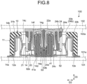
- FIG. 8 is a diagram illustrating a configuration taken along B-B of FIG. 4 in cross-section.
- the contact holding portion 41 includes a bottom surface portion 41a.
- the bottom surface portion 41a faces the substrate surface 101a of the first substrate 101.
- the bottom surface portion 41a has a shape in which the distance from a virtual plane S increases from the center to both ends in the width direction D2.
- the virtual plane S is a plane facing the bottom surface portion 41a.
- the substrate surface 101a is the virtual plane S.
- the bottom surface portion 41a may have a curved shape in which it is curved in its entirety in the width direction D2 or a curved shape in which it is curved only at both ends in the width direction D2.
- the curved shape of the bottom surface portion 41a prevents the contact between the bottom surface portion 41a and the substrate surface 101a even when the movable insulator 13 sways with an angle relative to the virtual plane S (the substrate surface 101a) in the width direction D2. This allows improvement in fitting performance and prevents damage to the first connector 10 during fitting or after fitting when, for example, the second connector 20 is fitted to the first connector 10 in a tilted state with respect to the fitting direction D3.
- the insert hole 42 is provided at the center of the contact holding portion 41 when viewed in the fitting direction D3. Part of the second connector 20 is inserted into the insert hole 42.
- the lock portion 43 is disposed at one end of the contact holding portion 41 in the contact array direction D1.
- the lock portion 44 is disposed at the other end of the contact holding portion 41 in the contact array direction D1.
- the lock portion 43 and the lock portion 44 are each inserted between the insulator support portion 12b of the metal fitting 12 and the substrate surface 101a.
- Each of the lock portion 43 and the lock portion 44 is arranged facing the protrusion portion 12d of the insulator support portion 12b.
- the arrangement of the lock portion 43 and the lock portion 44 so as to face the protrusion portion 12d restricts the movement of the movable insulator 13 in the fitting direction D3. That is, the movable insulator 13 is held so as not to be removed from the fixing insulator 11. Since each of the lock portion 43 and the lock portion 44 is locally in contact with the protrusion portion 12d, not the entire insulator support portion 12b, sliding resistance is reduced.
- a width L1 that is the dimension of the lock portion 43 and the lock portion 44 in the width direction D2 (the dimension in the width direction D2 is hereinafter referred to as a width) is larger than a width L2 of the contact holding portion 41 (see FIG. 4 ).
- the width L1 being larger than the width L2 allows the movable insulator 13 to have improved strength of the lock portion 43 and the lock portion 44.
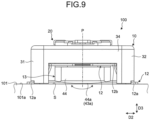
- FIG. 9 is a side view illustrating an example of the connector 100.
- FIG. 9 illustrates the connector 100 when viewed from the beam portion 34 side of the first connector 10.
- the lock portion 44 includes a bottom surface portion 44a.
- the bottom surface portion 44a faces the substrate surface 101a of the first substrate 101.
- the bottom surface portion 44a has a shape in which the distance from the virtual plane S increases from the center to both ends in the width direction D2.
- the virtual plane S is the plane facing the bottom surface portion 44a.
- the substrate surface 101a is the virtual plane S.
- the bottom surface portion 44a may have a curved shape in its entirety in the width direction D2 or a curved shape in which it is curved only at both ends in the width direction D2.
- the bottom surface portion 44a may be coplanar with the bottom surface portion 41a of the contact holding portion 41.
- a bottom surface portion 43a (see FIG. 4 ) of the lock portion 43 has the same configuration as that of the bottom surface portion 44a of the lock portion 44.
- the curved shapes of the bottom surface portion 43a and the bottom surface portion 44a prevent the contact between the bottom surface portion 43a and the bottom surface portion 44a and the substrate surface 101a even when the movable insulator 13 sways in the width direction D2.
- the first connector 10 thus allows the movable insulator 13 to sway in the width direction D2.
- the contacts 14 are arranged alongside in the contact array direction D1.
- the contacts 14 are formed by, for example, conducting bending processing on a metallic material.
- the method for forming the contacts 14 is not limited to the bending processing, and the contacts 14 may be formed by, for example, conducing die-cut processing on a metallic material.
- the contacts 14 each include a mounting portion 14a, a first lock portion 14b, an elastic deformation portion 14c, a second lock portion 14d, a third lock portion 14e, a first connection portion 14f, and a second connection portion 14g.
- the mounting portion 14a is mounted on the substrate surface 101a.
- the first lock portion 14b is locked with the fixing insulator 11.
- the elastic deformation portion 14c is a portion that is disposed between the first lock portion 14b and the second lock portion 14d, and that can be elastically deformed.
- the second lock portion 14d and the third lock portion 14e are locked with the contact holding portion 41 of the movable insulator 13.
- the first connection portion 14f and the second connection portion 14g are in contact with a contact 24 of the second connector 20.
- the first connection portion 14f is disposed closer to the fixing insulator 11.
- the second connection portion 14g is disposed inside the insert hole 42.
- the second connector 20 is fixed to a second substrate 102.
- the second connector 20 includes an insulator 21, metal fittings 22, and the contacts 24.
- the insulator 21 is formed in a rectangular shape by using, for example, a resin material.
- the insulator 21 is disposed with a spacing from a substrate surface 102a of the second substrate 102.
- the insulator 21 includes a contact holding portion 51, an outer insertion portion 52, and an inner insertion portion 53.
- the contact holding portion 51 is disposed facing the substrate surface 102a.
- the contact holding portion 51 extends in parallel to the contact array direction D1.
- the contact holding portion 51 holds the contacts 24.
- the contact holding portion 51 includes groove portions 51b (see FIG. 3 ) that hold the contacts 24.
- the groove portions 51b are arranged alongside at a predetermined interval in the contact array direction D1.
- the interval between the two adjacent groove portions 51b is the same as the interval between the two adjacent groove portions 41b of the contact holding portion 41 in the first connector 10.
- the outer insertion portion 52 is integrally formed with the contact holding portion 51.
- the outer insertion portion 52 is formed in a ring shape (see FIG. 6 ).
- the outer insertion portion 52 is disposed between the wall portion 31, the wall portion 32, the beam portion 33, and the beam portion 34 of the fixing insulator 11 and the contact holding portion 41 of the movable insulator 13.
- the outer insertion portion 52 is provided at a position to surround the contact holding portion 41.
- the outer insertion portion 52 includes a fitting surface 52b caused to face the first connector 10 at the time of the fitting (see FIG. 6 ).
- the inner insertion portion 53 is integrally formed with the contact holding portion 51.
- the inner insertion portion 53 is provided inside the outer insertion portion 52 (see FIG. 6 ).
- the inner insertion portion 53 is formed in a plate-like shape.
- the inner insertion portion 53 is inserted into the insert hole 42 of the movable insulator 13 when the second connector 20 is fitted to the first connector 10.
- the inner insertion portion 53 includes a fitting surface 53b caused to face the first connector 10 at the time of the fitting (see FIG. 6 ).
- the metal fittings 22 have, for example, a plate-like shape.
- the metal fittings 22 each include a mounting portion 22a and an insulator lock portion 22b.
- One of the mounting portions 22a is provided at one end of the insulator 21 and another one of the mounting portions 22a at the other end of the insulator 21, and the mounting portions 22a are arranged in parallel to the substrate surface 102a.
- the mounting portion 22a is fixed to the substrate surface 102a.
- the insulator lock portion 22b is bent with respect to the mounting portion 22a toward the inside of the insulator 21.
- the insulator lock portion 22b is locked with the insulator 21 in a state of being inserted into a metal fitting holding section 21b of the insulator 21.
- the contacts 24 are arranged alongside in the contact array direction D1.
- the contact 24 is formed by, for example, conducting die-cut processing on a metallic material.
- the method for forming the contacts 24 is not limited to the die-cut processing, and the contacts 24 may be formed by conducting, for example, bending processing on a metallic material.
- the contacts 24 each include a mounting portion 24a, a lock portion 24b, a first connection portion 24c, and a second connection portion 24d.
- the mounting portion 24a is mounted on the substrate surface 102a.
- the lock portion 24b is locked with the contact holding portion 51 of the insulator 21.
- the first connection portion 24c is disposed on the inner periphery of the outer insertion portion 52.
- the first connection portion 24c is connected to the first connection portion 14f of the contact 14 provided in the first connector 10.
- the second connection portion 24d is disposed on the outer periphery of the inner insertion portion 53.
- the second connection portion 24d is connected to the second connection portion 14g of the contact 14 provided in the first connector 10.
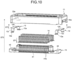
- FIG. 10 is a diagram illustrating the flow of assembling the first connector 10.
- a first assembly step (ST1 in FIG. 10 ) will be explained.
- the contacts 14 are inserted into the groove portions 41b of the movable insulator 13 from above. This step allows the contacts 14 to be locked and held by the movable insulator 13.
- a second assembly step (ST2 in FIG. 10 ) will be explained.
- the metal fittings 12 are inserted into the fixing insulator 11 from beneath.
- the insulator support portions 12b abut the support surface 33a and the support surface 34a of the fixing insulator 11.
- the step allows the insulator lock portions 12c to be locked with the fixing insulator 11.
- the metal fittings 12 are locked with the fixing insulator 11 in a state of being disposed inside the fixing insulator 11, i.e., in a state of being not exposed on the surface at the fitting side of the fixing insulator 11. Either one of the first assembly step and the second assembly step may be performed first.
- a third assembly step (ST3 in FIG. 10 ) will be explained.
- the movable insulator 13 holding the contacts 14 is inserted into the fixing insulator 11, with which the metal fittings 12 are locked, from beneath.
- This step allows the movable insulator 13 to be disposed inside the fixing insulator 11 in a state where the lock portion 43 and the lock portion 44 of the movable insulator 13 face or abut the respective metal fittings 12. Assembling of the first connector 10 is thus completed.
- FIG. 11 is a diagram illustrating the flow of assembling the second connector 20.
- a fourth assembly step (ST4 in FIG. 11 ) will be explained.
- the contacts 24 are inserted into the groove portions 51b of the insulator 21 from above. The step allows the contacts 24 to be locked and held by the insulator 21.
- a fifth assembly step (ST5 in FIG. 11 ) will be explained.
- the metal fittings 22 are inserted into the respective metal fitting holding sections 21b of the insulator 21 from above.
- the insulator lock portions 22b are locked with the insulator 21 inside the respective metal fitting holding sections 21b. Assembling of the second connector 20 is thus completed. Either one of the fourth assembly step and the fifth assembly step may be conducted first.
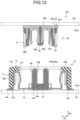
- FIG. 12 is a diagram illustrating a state where the first connector 10 faces the second connector 20.
- the fitting surface 31b, the fitting surface 32b, the fitting surface 33b, and the fitting surface 34b of the first connector 10 face the fitting surface 52b and the fitting surface 53b of the second connector 20.
- the first connector 10 and the second connector 20 are moved relative to each other to adjust positions.
- the fixing insulator 11 of the first connector 10 and the insulator 21 of the second connector 20 are brought into contact with each other, and caused to slide in a direction perpendicular to the fitting direction D3.
- the fitting surface 31b, the fitting surface 32b, the fitting surface 33b, and the fitting surface 34b of the fixing insulator 11 are flat. Consequently, the second connector 20 smoothly moves on the fitting surface 31b, the fitting surface 32b, the fitting surface 33b, and the fitting surface 34b.
- the positional adjustment allows the outer insertion portion 52 of the insulator 21 to be inserted between the fixing insulator 11 and the contact holding portion 41 of the first connector 10, and allows the inner insertion portion 53 to be inserted into the insert hole 42.
- This allows fitting among the fixing insulator 11, the movable insulator 13, and the insulator 21.
- the fitting brings the first connection portion 24c of the contact 24 in contact with the first connection portion 14f of the contact 14.
- the fitting also brings the second connection portion 24d of the contact 24 in contact with the second connection portion 14g of the contact 14. Consequently, the contacts 14 are electrically connected to the contacts 24.
- the movable insulator 13 sways in the width direction D2. Accordingly, when the fixing insulator 11 and the movable insulator 13 of the first connector 10 are fitted to the insulator 21 of the second connector 20 in a state of being shifted in the width direction D2, for example, the positional relation between the first connector 10 and the second connector 20 is easily corrected by the movable insulator 13 swaying in the width direction D2.
- the bottom surface portion 41a, the bottom surface portion 43a, and the bottom surface portion 44a are curved, the bottom surface portion 41a, the bottom surface portion 43a, and the bottom surface portion 44a are prevented from being in contact with the substrate surface 101a even when the movable insulator 13 sways in the width direction D2.
- the outer insertion portion 52 of the insulator 21 is pulled out from between the fixing insulator 11 and the contact holding portion 41, and the inner insertion portion 53 is pulled out from the insert hole 42.
- the first connection portion 24c and the first connection portion 14f are separated from each other, and the second connection portion 24d and the second connection portion 14g are separated from each other.
- the contact 14 and the contact 24 are electrically disconnected.
- the lock portion 43 is disposed at one end of the movable insulator 13 in the contact array direction D1 and the lock portion 44 at the other end of the movable insulator 13 in the contact array direction D1 such that the lock portions 43 and 44 face the respective metal fittings 12. Accordingly, if the movable insulator 13 is pulled toward the second connector 20 when the second connector 20 is removed from the first connector 10 or when unintentional force is applied, the metal fittings 12 restrict the movement of the movable insulator 13 in the fitting direction D3 (in the direction to remove the second connector 20).
- the metal fittings 12 are locked with the fixing insulator 11 in a state of being disposed inside the fixing insulator 11, i.e., in a state of being not exposed on the fitting surface 31b, the fitting surface 32b, the fitting surface 33b, and the fitting surface 34b of the fixing insulator 11. Accordingly, in comparison with a case where the metal fittings 12 are disposed on the surface of the fixing insulator 11, damage to other connectors caused by metallic fittings is suppressed, or unevenness of the surface of the fixing insulator 11 is reduced.
- the connector 100 can reduce its size, prevent a decrease in strength, and improve fitting performance when the first connector 10 and the second connector 20 are fitted to each other.
- the movable insulator 13 has the lock portion 43 and the lock portion 44, the width L1 of which is larger than the width L2 of the contact holding portion 41. Accordingly, even when the width L2 of the contact holding portion 41 is made smaller for downsizing, a reduction in strength of the movable insulator 13 can be prevented.
- the entire surfaces of the fitting surface 31b, the fitting surface 32b, the fitting surface 33b, and the fitting surface 34b are exposed to the second connector 20.
- the fitting surface 31b, the fitting surface 32b, the fitting surface 33b, and the fitting surface 34b for guiding the second connector 20 are coplanar and flat surfaces in the fixing insulator 11.
- the fitting surface 31b, the fitting surface 32b, the fitting surface 33b, and the fitting surface 34b are flat and continuously formed on the whole circumference of the fixing insulator 11.
- the second connector 20 can smoothly move on the fitting surface 31b, the fitting surface 32b, the fitting surface 33b, and 34b, and they are not damaged by metallic fittings or the like. This allows the second connector 20 to be easily and securely guided, thereby improving operational performance for fitting task.
- the bottom surface portion 41a and the bottom surface portion 44a of the movable insulator 13 facing the substrate surface 101a have a shape in which the distance from the substrate surface 101a increases from the center to both ends in the width direction D2. Accordingly, even when the movable insulator 13 sways in the width direction D2, the bottom surface portion 41a and the bottom surface portion 44a can be prevented from being in contact with the substrate surface 101a.
- the technical scope of the present invention is not limited to embodiments, and modifications may be appropriately made without departing from the scope of the present invention.
- the explanation given to embodiments takes an example in which, at a contact portion between the insulator support portion 12b and each of the lock portion 43 and the lock portion 44, the protrusion portion 12d is provided to the insulator support portion 12b.
- the protrusion portion may be provided to each of the lock portion 43 and the lock portion 44.
- the protrusion portions may be provided to both the insulator support portions 12b and to the lock portion 43 and the lock portion 44.
- the explanation given to embodiments takes an example in which the bottom surface portion 41a, the bottom surface portion 43a, and the bottom surface portion 44a of the movable insulator 13 each have a curved shape.
- the shape of the movable insulator 13 may be other shapes as long as the bottom surface portion 41a, the bottom surface portion 43a, and the bottom surface portion 44a are configured not to be in contact with the substrate surface 101a when the movable insulator 13 sways in the width direction D2.
- the bottom surface portion 41a, the bottom surface portion 43a, and the bottom surface portion 44a may have a planar shape parallel to the virtual plane S (the substrate surface 101a) at the central part in the width direction D2, and have a curved shape partially at both ends in the width direction D2.
- the bottom surface portion 41a, the bottom surface portion 43a, and the bottom surface portion 44a may have a planar shape (inclined plane), in which the distance from the substrate surface 101a increases from the center to both ends in the width direction D2.
- the inclined plane may be provided entirely from the center to both ends in the width direction D2, or the inclined plane may be provided partially at both ends in the width direction D2, while the central part in the width direction D2 has a planar shape parallel to the virtual plane S (the substrate surface 101a).
Landscapes
- Coupling Device And Connection With Printed Circuit (AREA)
- Details Of Connecting Devices For Male And Female Coupling (AREA)
Applications Claiming Priority (2)
| Application Number | Priority Date | Filing Date | Title |
|---|---|---|---|
| JP2016158225 | 2016-08-10 | ||
| PCT/JP2017/029147 WO2018030522A1 (ja) | 2016-08-10 | 2017-08-10 | コネクタ |
Publications (3)
| Publication Number | Publication Date |
|---|---|
| EP3499651A1 EP3499651A1 (en) | 2019-06-19 |
| EP3499651A4 EP3499651A4 (en) | 2020-04-08 |
| EP3499651B1 true EP3499651B1 (en) | 2025-06-25 |
Family
ID=61163105
Family Applications (1)
| Application Number | Title | Priority Date | Filing Date |
|---|---|---|---|
| EP17839586.9A Active EP3499651B1 (en) | 2016-08-10 | 2017-08-10 | Connector |
Country Status (6)
Families Citing this family (13)
| Publication number | Priority date | Publication date | Assignee | Title |
|---|---|---|---|---|
| JP6727074B2 (ja) * | 2016-08-29 | 2020-07-22 | ヒロセ電機株式会社 | 回路基板用電気コネクタ |
| JP6270294B1 (ja) * | 2016-11-24 | 2018-01-31 | イリソ電子工業株式会社 | 可動コネクタ |
| JP7196468B2 (ja) | 2018-08-29 | 2022-12-27 | 大同特殊鋼株式会社 | R-t-b系焼結磁石 |
| TWI711232B (zh) * | 2019-06-17 | 2020-11-21 | 唐虞企業股份有限公司 | 電連接器 |
| JP6687790B1 (ja) | 2019-07-26 | 2020-04-28 | 京セラ株式会社 | コネクタ及び電子機器 |
| CN112864660A (zh) * | 2021-01-20 | 2021-05-28 | 宁波西创尼克电子科技有限公司 | 一种用于显示屏组件的浮动连接器及显示屏组件 |
| JP2022123714A (ja) * | 2021-02-12 | 2022-08-24 | 京セラ株式会社 | コネクタ及び電子機器 |
| JP1719683S (ja) * | 2021-09-30 | 2022-07-13 | 電気コネクタ | |
| JP1719731S (ja) * | 2021-09-30 | 2022-07-13 | 電気コネクタ | |
| JP1719682S (ja) * | 2021-09-30 | 2022-07-13 | 電気コネクタ | |
| KR20250033268A (ko) * | 2022-07-20 | 2025-03-07 | 동관 엘제이브이 테크놀로지 컴퍼니 리미티드 | 요동형 허용오차 커넥터 및 요동형 허용오차 플로팅 커넥터 |
| CN115332875A (zh) * | 2022-07-20 | 2022-11-11 | 东莞市林积为实业投资有限公司 | 摆式容差连接器 |
| JP1749340S (ja) * | 2023-01-10 | 2023-07-25 | コネクタ |
Citations (2)
| Publication number | Priority date | Publication date | Assignee | Title |
|---|---|---|---|---|
| JP2006216298A (ja) * | 2005-02-02 | 2006-08-17 | Honda Tsushin Kogyo Co Ltd | フローティング型電気コネクタ |
| EP3399596A1 (en) * | 2015-12-28 | 2018-11-07 | KYOCERA Corporation | Floating connector device |
Family Cites Families (25)
| Publication number | Priority date | Publication date | Assignee | Title |
|---|---|---|---|---|
| JP2568142B2 (ja) | 1991-12-30 | 1996-12-25 | モレックス インコーポレーテッド | フローティング構造の電気コネクタ及びその製法 |
| JPH06163125A (ja) | 1992-11-25 | 1994-06-10 | Matsushita Electric Works Ltd | 基板対基板用コネクタ |
| JP3007812U (ja) * | 1994-05-25 | 1995-02-28 | モレックス インコーポレーテッド | 表面実装用電気コネクタ |
| JPH09320708A (ja) | 1996-05-31 | 1997-12-12 | Matsushita Electric Works Ltd | フローティングコネクタ |
| JPH10312868A (ja) * | 1997-05-13 | 1998-11-24 | Sumitomo Wiring Syst Ltd | 基板用コネクタ |
| JPH10326651A (ja) | 1997-05-27 | 1998-12-08 | Sumitomo Wiring Syst Ltd | 基板用コネクタ |
| US8014974B2 (en) * | 2001-12-19 | 2011-09-06 | Caterpillar Inc. | System and method for analyzing and reporting machine operating parameters |
| JP2004063358A (ja) * | 2002-07-31 | 2004-02-26 | Hirose Electric Co Ltd | フローティング電気コネクタ |
| JP4411843B2 (ja) * | 2003-01-22 | 2010-02-10 | Smk株式会社 | フローティングコネクタ |
| JP3929946B2 (ja) | 2003-07-29 | 2007-06-13 | 矢崎総業株式会社 | コネクタ |
| JP4287825B2 (ja) * | 2005-01-28 | 2009-07-01 | モレックス インコーポレイテド | 基板接続用コネクタ |
| JP2007018785A (ja) * | 2005-07-06 | 2007-01-25 | D D K Ltd | コネクタ |
| JP4969838B2 (ja) * | 2005-11-28 | 2012-07-04 | モレックス インコーポレイテド | フローティングタイプコネクタ |
| JP2007220327A (ja) | 2006-02-14 | 2007-08-30 | Kel Corp | フローティング型コネクタ |
| JP5166931B2 (ja) | 2008-03-21 | 2013-03-21 | 第一電子工業株式会社 | 電気コネクタ |
| JP5000560B2 (ja) | 2008-03-21 | 2012-08-15 | 第一電子工業株式会社 | 電気コネクタ |
| JP5185731B2 (ja) * | 2008-08-27 | 2013-04-17 | 第一電子工業株式会社 | フローティングコネクタ用固定具及び該固定具を用いるフローティングコネクタ |
| JP4374074B1 (ja) * | 2009-06-10 | 2009-12-02 | イリソ電子工業株式会社 | 電気接続用端子及びこれを用いたコネクタ |
| JP2011249076A (ja) * | 2010-05-25 | 2011-12-08 | Fujitsu Component Ltd | フローティングコネクタ |
| JP5590991B2 (ja) * | 2010-06-30 | 2014-09-17 | 京セラコネクタプロダクツ株式会社 | コネクタ |
| KR20150051997A (ko) | 2012-09-05 | 2015-05-13 | 이리소 일렉트로닉스 컴패니 리미티드 | 커넥터 |
| JP5499191B1 (ja) * | 2013-01-28 | 2014-05-21 | 日本航空電子工業株式会社 | コネクタ |
| JP5946804B2 (ja) | 2013-08-09 | 2016-07-06 | ヒロセ電機株式会社 | コネクタ |
| US9391398B2 (en) * | 2014-03-20 | 2016-07-12 | Japan Aviation Electronics Industry, Limited | Connector assembly |
| JP6771989B2 (ja) * | 2016-08-09 | 2020-10-21 | ヒロセ電機株式会社 | 回路基板用電気コネクタ |
-
2017
- 2017-08-10 CN CN201780048679.3A patent/CN109565123B/zh active Active
- 2017-08-10 EP EP17839586.9A patent/EP3499651B1/en active Active
- 2017-08-10 WO PCT/JP2017/029147 patent/WO2018030522A1/ja active IP Right Grant
- 2017-08-10 US US16/324,085 patent/US10833443B2/en active Active
- 2017-08-10 KR KR1020197003731A patent/KR102202564B1/ko active Active
- 2017-08-10 JP JP2018502029A patent/JP6371491B2/ja active Active
-
2018
- 2018-07-12 JP JP2018132591A patent/JP6656317B2/ja active Active
- 2018-07-12 JP JP2018132450A patent/JP2018160471A/ja active Pending
-
2019
- 2019-06-25 JP JP2019117547A patent/JP2019186219A/ja active Pending
Patent Citations (2)
| Publication number | Priority date | Publication date | Assignee | Title |
|---|---|---|---|---|
| JP2006216298A (ja) * | 2005-02-02 | 2006-08-17 | Honda Tsushin Kogyo Co Ltd | フローティング型電気コネクタ |
| EP3399596A1 (en) * | 2015-12-28 | 2018-11-07 | KYOCERA Corporation | Floating connector device |
Also Published As
| Publication number | Publication date |
|---|---|
| CN109565123B (zh) | 2020-12-22 |
| JP2019186219A (ja) | 2019-10-24 |
| EP3499651A4 (en) | 2020-04-08 |
| JP2018160471A (ja) | 2018-10-11 |
| US20190214762A1 (en) | 2019-07-11 |
| KR102202564B1 (ko) | 2021-01-13 |
| KR20190026011A (ko) | 2019-03-12 |
| EP3499651A1 (en) | 2019-06-19 |
| US10833443B2 (en) | 2020-11-10 |
| CN109565123A (zh) | 2019-04-02 |
| WO2018030522A1 (ja) | 2018-02-15 |
| JP2018160472A (ja) | 2018-10-11 |
| JPWO2018030522A1 (ja) | 2018-08-09 |
| JP6656317B2 (ja) | 2020-03-04 |
| JP6371491B2 (ja) | 2018-08-08 |
Similar Documents
| Publication | Publication Date | Title |
|---|---|---|
| EP3499651B1 (en) | Connector | |
| EP1990868B1 (en) | Electrical connector | |
| US10530090B2 (en) | Holding frame for a plug connector and methods of populating same | |
| WO2018034325A1 (ja) | コネクタ | |
| US12003049B2 (en) | Connector and electronic device | |
| US11605913B2 (en) | Connector and manufacturing method of connector | |
| US20150194752A1 (en) | Electrical connector having compliant contacts and a circuit board assembly including the same | |
| US20200169040A1 (en) | Connector and connection structure | |
| US11177589B2 (en) | Electrical terminal and electrical connector thereof | |
| US20220393383A1 (en) | Terminal position assurance device and corresponding connector assembly | |
| US9960517B2 (en) | Electrical contact terminal having a spring element to support a contact beam | |
| CN100544127C (zh) | 电缆连接器、电缆连接器组件和用于其的套圈系统 | |
| US10770252B2 (en) | Magnetic system of electromagnetic relay | |
| US11404819B2 (en) | Contact device, contact system having such a contact device and method for producing such a contact system | |
| KR20200002119U (ko) | 플로팅 버스바 연결 어셈블리 | |
| US9116316B2 (en) | Optical connector, male connector housing for optical connector, and female connector housing for optical connector | |
| EP3267533A1 (en) | Connection terminal and electrical connector | |
| KR101412322B1 (ko) | 커넥터 | |
| JP7098678B2 (ja) | プロテクタおよびワイヤハーネス | |
| EP3648261A1 (en) | Rounded connector assembly | |
| CN119155930A (zh) | 用于壳体的连接元件、壳体及其组装方法 | |
| US20230029814A1 (en) | Connector Cage Assembly | |
| US20250105554A1 (en) | Connector | |
| JP2008262897A (ja) | 端子および端子と基板との接続構造 | |
| US10326226B2 (en) | Contact with a first cylindrical section, a second cylindrical section, and a transition section and a connector using the same |
Legal Events
| Date | Code | Title | Description |
|---|---|---|---|
| STAA | Information on the status of an ep patent application or granted ep patent |
Free format text: STATUS: THE INTERNATIONAL PUBLICATION HAS BEEN MADE |
|
| PUAI | Public reference made under article 153(3) epc to a published international application that has entered the european phase |
Free format text: ORIGINAL CODE: 0009012 |
|
| STAA | Information on the status of an ep patent application or granted ep patent |
Free format text: STATUS: REQUEST FOR EXAMINATION WAS MADE |
|
| 17P | Request for examination filed |
Effective date: 20190206 |
|
| AK | Designated contracting states |
Kind code of ref document: A1 Designated state(s): AL AT BE BG CH CY CZ DE DK EE ES FI FR GB GR HR HU IE IS IT LI LT LU LV MC MK MT NL NO PL PT RO RS SE SI SK SM TR |
|
| AX | Request for extension of the european patent |
Extension state: BA ME |
|
| DAV | Request for validation of the european patent (deleted) | ||
| DAX | Request for extension of the european patent (deleted) | ||
| A4 | Supplementary search report drawn up and despatched |
Effective date: 20200311 |
|
| RIC1 | Information provided on ipc code assigned before grant |
Ipc: H01R 12/72 20110101ALN20200305BHEP Ipc: H01R 13/631 20060101ALI20200305BHEP Ipc: H01R 12/91 20110101AFI20200305BHEP Ipc: H01R 12/73 20110101ALN20200305BHEP |
|
| STAA | Information on the status of an ep patent application or granted ep patent |
Free format text: STATUS: EXAMINATION IS IN PROGRESS |
|
| STAA | Information on the status of an ep patent application or granted ep patent |
Free format text: STATUS: EXAMINATION IS IN PROGRESS |
|
| 17Q | First examination report despatched |
Effective date: 20210908 |
|
| P01 | Opt-out of the competence of the unified patent court (upc) registered |
Effective date: 20230505 |
|
| GRAP | Despatch of communication of intention to grant a patent |
Free format text: ORIGINAL CODE: EPIDOSNIGR1 |
|
| STAA | Information on the status of an ep patent application or granted ep patent |
Free format text: STATUS: GRANT OF PATENT IS INTENDED |
|
| RIC1 | Information provided on ipc code assigned before grant |
Ipc: H01R 12/73 20110101ALN20250111BHEP Ipc: H01R 12/72 20110101ALN20250111BHEP Ipc: H01R 13/631 20060101ALI20250111BHEP Ipc: H01R 12/91 20110101AFI20250111BHEP |
|
| INTG | Intention to grant announced |
Effective date: 20250124 |
|
| GRAS | Grant fee paid |
Free format text: ORIGINAL CODE: EPIDOSNIGR3 |
|
| GRAA | (expected) grant |
Free format text: ORIGINAL CODE: 0009210 |
|
| STAA | Information on the status of an ep patent application or granted ep patent |
Free format text: STATUS: THE PATENT HAS BEEN GRANTED |
|
| AK | Designated contracting states |
Kind code of ref document: B1 Designated state(s): AL AT BE BG CH CY CZ DE DK EE ES FI FR GB GR HR HU IE IS IT LI LT LU LV MC MK MT NL NO PL PT RO RS SE SI SK SM TR |
|
| REG | Reference to a national code |
Ref country code: GB Ref legal event code: FG4D |
|
| REG | Reference to a national code |
Ref country code: CH Ref legal event code: EP |
|
| REG | Reference to a national code |
Ref country code: DE Ref legal event code: R096 Ref document number: 602017090170 Country of ref document: DE |
|
| REG | Reference to a national code |
Ref country code: CH Ref legal event code: EP |
|
| REG | Reference to a national code |
Ref country code: IE Ref legal event code: FG4D |