EP3492968A1 - Liquid-crystal variable retarder using liquid crystal cells of differing thicknesses - Google Patents
Liquid-crystal variable retarder using liquid crystal cells of differing thicknesses Download PDFInfo
- Publication number
- EP3492968A1 EP3492968A1 EP18209312.0A EP18209312A EP3492968A1 EP 3492968 A1 EP3492968 A1 EP 3492968A1 EP 18209312 A EP18209312 A EP 18209312A EP 3492968 A1 EP3492968 A1 EP 3492968A1
- Authority
- EP
- European Patent Office
- Prior art keywords
- liquid
- crystal
- retardance
- variable retarder
- cell
- Prior art date
- Legal status (The legal status is an assumption and is not a legal conclusion. Google has not performed a legal analysis and makes no representation as to the accuracy of the status listed.)
- Withdrawn
Links
Images

Classifications
-
- G—PHYSICS
- G09—EDUCATION; CRYPTOGRAPHY; DISPLAY; ADVERTISING; SEALS
- G09G—ARRANGEMENTS OR CIRCUITS FOR CONTROL OF INDICATING DEVICES USING STATIC MEANS TO PRESENT VARIABLE INFORMATION
- G09G3/00—Control arrangements or circuits, of interest only in connection with visual indicators other than cathode-ray tubes
- G09G3/20—Control arrangements or circuits, of interest only in connection with visual indicators other than cathode-ray tubes for presentation of an assembly of a number of characters, e.g. a page, by composing the assembly by combination of individual elements arranged in a matrix no fixed position being assigned to or needed to be assigned to the individual characters or partial characters
- G09G3/34—Control arrangements or circuits, of interest only in connection with visual indicators other than cathode-ray tubes for presentation of an assembly of a number of characters, e.g. a page, by composing the assembly by combination of individual elements arranged in a matrix no fixed position being assigned to or needed to be assigned to the individual characters or partial characters by control of light from an independent source
- G09G3/36—Control arrangements or circuits, of interest only in connection with visual indicators other than cathode-ray tubes for presentation of an assembly of a number of characters, e.g. a page, by composing the assembly by combination of individual elements arranged in a matrix no fixed position being assigned to or needed to be assigned to the individual characters or partial characters by control of light from an independent source using liquid crystals
-
- G—PHYSICS
- G01—MEASURING; TESTING
- G01J—MEASUREMENT OF INTENSITY, VELOCITY, SPECTRAL CONTENT, POLARISATION, PHASE OR PULSE CHARACTERISTICS OF INFRARED, VISIBLE OR ULTRAVIOLET LIGHT; COLORIMETRY; RADIATION PYROMETRY
- G01J3/00—Spectrometry; Spectrophotometry; Monochromators; Measuring colours
- G01J3/28—Investigating the spectrum
-
- G—PHYSICS
- G02—OPTICS
- G02F—OPTICAL DEVICES OR ARRANGEMENTS FOR THE CONTROL OF LIGHT BY MODIFICATION OF THE OPTICAL PROPERTIES OF THE MEDIA OF THE ELEMENTS INVOLVED THEREIN; NON-LINEAR OPTICS; FREQUENCY-CHANGING OF LIGHT; OPTICAL LOGIC ELEMENTS; OPTICAL ANALOGUE/DIGITAL CONVERTERS
- G02F1/00—Devices or arrangements for the control of the intensity, colour, phase, polarisation or direction of light arriving from an independent light source, e.g. switching, gating or modulating; Non-linear optics
- G02F1/01—Devices or arrangements for the control of the intensity, colour, phase, polarisation or direction of light arriving from an independent light source, e.g. switching, gating or modulating; Non-linear optics for the control of the intensity, phase, polarisation or colour
- G02F1/13—Devices or arrangements for the control of the intensity, colour, phase, polarisation or direction of light arriving from an independent light source, e.g. switching, gating or modulating; Non-linear optics for the control of the intensity, phase, polarisation or colour based on liquid crystals, e.g. single liquid crystal display cells
- G02F1/137—Devices or arrangements for the control of the intensity, colour, phase, polarisation or direction of light arriving from an independent light source, e.g. switching, gating or modulating; Non-linear optics for the control of the intensity, phase, polarisation or colour based on liquid crystals, e.g. single liquid crystal display cells characterised by the electro-optical or magneto-optical effect, e.g. field-induced phase transition, orientation effect, guest-host interaction or dynamic scattering
- G02F1/139—Devices or arrangements for the control of the intensity, colour, phase, polarisation or direction of light arriving from an independent light source, e.g. switching, gating or modulating; Non-linear optics for the control of the intensity, phase, polarisation or colour based on liquid crystals, e.g. single liquid crystal display cells characterised by the electro-optical or magneto-optical effect, e.g. field-induced phase transition, orientation effect, guest-host interaction or dynamic scattering based on orientation effects in which the liquid crystal remains transparent
- G02F1/1393—Devices or arrangements for the control of the intensity, colour, phase, polarisation or direction of light arriving from an independent light source, e.g. switching, gating or modulating; Non-linear optics for the control of the intensity, phase, polarisation or colour based on liquid crystals, e.g. single liquid crystal display cells characterised by the electro-optical or magneto-optical effect, e.g. field-induced phase transition, orientation effect, guest-host interaction or dynamic scattering based on orientation effects in which the liquid crystal remains transparent the birefringence of the liquid crystal being electrically controlled, e.g. ECB-, DAP-, HAN-, PI-LC cells
- G02F1/1395—Optically compensated birefringence [OCB]- cells or PI- cells
-
- G—PHYSICS
- G01—MEASURING; TESTING
- G01J—MEASUREMENT OF INTENSITY, VELOCITY, SPECTRAL CONTENT, POLARISATION, PHASE OR PULSE CHARACTERISTICS OF INFRARED, VISIBLE OR ULTRAVIOLET LIGHT; COLORIMETRY; RADIATION PYROMETRY
- G01J3/00—Spectrometry; Spectrophotometry; Monochromators; Measuring colours
- G01J3/28—Investigating the spectrum
- G01J3/2823—Imaging spectrometer
-
- G—PHYSICS
- G01—MEASURING; TESTING
- G01J—MEASUREMENT OF INTENSITY, VELOCITY, SPECTRAL CONTENT, POLARISATION, PHASE OR PULSE CHARACTERISTICS OF INFRARED, VISIBLE OR ULTRAVIOLET LIGHT; COLORIMETRY; RADIATION PYROMETRY
- G01J3/00—Spectrometry; Spectrophotometry; Monochromators; Measuring colours
- G01J3/28—Investigating the spectrum
- G01J3/447—Polarisation spectrometry
-
- G—PHYSICS
- G01—MEASURING; TESTING
- G01J—MEASUREMENT OF INTENSITY, VELOCITY, SPECTRAL CONTENT, POLARISATION, PHASE OR PULSE CHARACTERISTICS OF INFRARED, VISIBLE OR ULTRAVIOLET LIGHT; COLORIMETRY; RADIATION PYROMETRY
- G01J3/00—Spectrometry; Spectrophotometry; Monochromators; Measuring colours
- G01J3/28—Investigating the spectrum
- G01J3/45—Interferometric spectrometry
- G01J3/453—Interferometric spectrometry by correlation of the amplitudes
- G01J3/4531—Devices without moving parts
-
- G—PHYSICS
- G01—MEASURING; TESTING
- G01J—MEASUREMENT OF INTENSITY, VELOCITY, SPECTRAL CONTENT, POLARISATION, PHASE OR PULSE CHARACTERISTICS OF INFRARED, VISIBLE OR ULTRAVIOLET LIGHT; COLORIMETRY; RADIATION PYROMETRY
- G01J4/00—Measuring polarisation of light
- G01J4/04—Polarimeters using electric detection means
-
- G—PHYSICS
- G02—OPTICS
- G02B—OPTICAL ELEMENTS, SYSTEMS OR APPARATUS
- G02B5/00—Optical elements other than lenses
- G02B5/30—Polarising elements
- G02B5/3083—Birefringent or phase retarding elements
-
- G—PHYSICS
- G02—OPTICS
- G02F—OPTICAL DEVICES OR ARRANGEMENTS FOR THE CONTROL OF LIGHT BY MODIFICATION OF THE OPTICAL PROPERTIES OF THE MEDIA OF THE ELEMENTS INVOLVED THEREIN; NON-LINEAR OPTICS; FREQUENCY-CHANGING OF LIGHT; OPTICAL LOGIC ELEMENTS; OPTICAL ANALOGUE/DIGITAL CONVERTERS
- G02F1/00—Devices or arrangements for the control of the intensity, colour, phase, polarisation or direction of light arriving from an independent light source, e.g. switching, gating or modulating; Non-linear optics
- G02F1/01—Devices or arrangements for the control of the intensity, colour, phase, polarisation or direction of light arriving from an independent light source, e.g. switching, gating or modulating; Non-linear optics for the control of the intensity, phase, polarisation or colour
- G02F1/13—Devices or arrangements for the control of the intensity, colour, phase, polarisation or direction of light arriving from an independent light source, e.g. switching, gating or modulating; Non-linear optics for the control of the intensity, phase, polarisation or colour based on liquid crystals, e.g. single liquid crystal display cells
- G02F1/1326—Liquid crystal optical waveguides or liquid crystal cells specially adapted for gating or modulating between optical waveguides
-
- G—PHYSICS
- G02—OPTICS
- G02F—OPTICAL DEVICES OR ARRANGEMENTS FOR THE CONTROL OF LIGHT BY MODIFICATION OF THE OPTICAL PROPERTIES OF THE MEDIA OF THE ELEMENTS INVOLVED THEREIN; NON-LINEAR OPTICS; FREQUENCY-CHANGING OF LIGHT; OPTICAL LOGIC ELEMENTS; OPTICAL ANALOGUE/DIGITAL CONVERTERS
- G02F1/00—Devices or arrangements for the control of the intensity, colour, phase, polarisation or direction of light arriving from an independent light source, e.g. switching, gating or modulating; Non-linear optics
- G02F1/01—Devices or arrangements for the control of the intensity, colour, phase, polarisation or direction of light arriving from an independent light source, e.g. switching, gating or modulating; Non-linear optics for the control of the intensity, phase, polarisation or colour
- G02F1/13—Devices or arrangements for the control of the intensity, colour, phase, polarisation or direction of light arriving from an independent light source, e.g. switching, gating or modulating; Non-linear optics for the control of the intensity, phase, polarisation or colour based on liquid crystals, e.g. single liquid crystal display cells
- G02F1/133—Constructional arrangements; Operation of liquid crystal cells; Circuit arrangements
- G02F1/13306—Circuit arrangements or driving methods for the control of single liquid crystal cells
- G02F1/13318—Circuits comprising a photodetector
-
- G—PHYSICS
- G02—OPTICS
- G02F—OPTICAL DEVICES OR ARRANGEMENTS FOR THE CONTROL OF LIGHT BY MODIFICATION OF THE OPTICAL PROPERTIES OF THE MEDIA OF THE ELEMENTS INVOLVED THEREIN; NON-LINEAR OPTICS; FREQUENCY-CHANGING OF LIGHT; OPTICAL LOGIC ELEMENTS; OPTICAL ANALOGUE/DIGITAL CONVERTERS
- G02F1/00—Devices or arrangements for the control of the intensity, colour, phase, polarisation or direction of light arriving from an independent light source, e.g. switching, gating or modulating; Non-linear optics
- G02F1/01—Devices or arrangements for the control of the intensity, colour, phase, polarisation or direction of light arriving from an independent light source, e.g. switching, gating or modulating; Non-linear optics for the control of the intensity, phase, polarisation or colour
- G02F1/13—Devices or arrangements for the control of the intensity, colour, phase, polarisation or direction of light arriving from an independent light source, e.g. switching, gating or modulating; Non-linear optics for the control of the intensity, phase, polarisation or colour based on liquid crystals, e.g. single liquid crystal display cells
- G02F1/133—Constructional arrangements; Operation of liquid crystal cells; Circuit arrangements
- G02F1/1333—Constructional arrangements; Manufacturing methods
- G02F1/1335—Structural association of cells with optical devices, e.g. polarisers or reflectors
- G02F1/133528—Polarisers
-
- G—PHYSICS
- G02—OPTICS
- G02F—OPTICAL DEVICES OR ARRANGEMENTS FOR THE CONTROL OF LIGHT BY MODIFICATION OF THE OPTICAL PROPERTIES OF THE MEDIA OF THE ELEMENTS INVOLVED THEREIN; NON-LINEAR OPTICS; FREQUENCY-CHANGING OF LIGHT; OPTICAL LOGIC ELEMENTS; OPTICAL ANALOGUE/DIGITAL CONVERTERS
- G02F1/00—Devices or arrangements for the control of the intensity, colour, phase, polarisation or direction of light arriving from an independent light source, e.g. switching, gating or modulating; Non-linear optics
- G02F1/01—Devices or arrangements for the control of the intensity, colour, phase, polarisation or direction of light arriving from an independent light source, e.g. switching, gating or modulating; Non-linear optics for the control of the intensity, phase, polarisation or colour
- G02F1/13—Devices or arrangements for the control of the intensity, colour, phase, polarisation or direction of light arriving from an independent light source, e.g. switching, gating or modulating; Non-linear optics for the control of the intensity, phase, polarisation or colour based on liquid crystals, e.g. single liquid crystal display cells
- G02F1/133—Constructional arrangements; Operation of liquid crystal cells; Circuit arrangements
- G02F1/1333—Constructional arrangements; Manufacturing methods
- G02F1/1335—Structural association of cells with optical devices, e.g. polarisers or reflectors
- G02F1/13363—Birefringent elements, e.g. for optical compensation
-
- G—PHYSICS
- G01—MEASURING; TESTING
- G01J—MEASUREMENT OF INTENSITY, VELOCITY, SPECTRAL CONTENT, POLARISATION, PHASE OR PULSE CHARACTERISTICS OF INFRARED, VISIBLE OR ULTRAVIOLET LIGHT; COLORIMETRY; RADIATION PYROMETRY
- G01J3/00—Spectrometry; Spectrophotometry; Monochromators; Measuring colours
- G01J3/28—Investigating the spectrum
- G01J2003/2866—Markers; Calibrating of scan
-
- G—PHYSICS
- G02—OPTICS
- G02B—OPTICAL ELEMENTS, SYSTEMS OR APPARATUS
- G02B27/00—Optical systems or apparatus not provided for by any of the groups G02B1/00 - G02B26/00, G02B30/00
- G02B27/28—Optical systems or apparatus not provided for by any of the groups G02B1/00 - G02B26/00, G02B30/00 for polarising
- G02B27/286—Optical systems or apparatus not provided for by any of the groups G02B1/00 - G02B26/00, G02B30/00 for polarising for controlling or changing the state of polarisation, e.g. transforming one polarisation state into another
-
- G—PHYSICS
- G02—OPTICS
- G02F—OPTICAL DEVICES OR ARRANGEMENTS FOR THE CONTROL OF LIGHT BY MODIFICATION OF THE OPTICAL PROPERTIES OF THE MEDIA OF THE ELEMENTS INVOLVED THEREIN; NON-LINEAR OPTICS; FREQUENCY-CHANGING OF LIGHT; OPTICAL LOGIC ELEMENTS; OPTICAL ANALOGUE/DIGITAL CONVERTERS
- G02F2201/00—Constructional arrangements not provided for in groups G02F1/00 - G02F7/00
- G02F2201/58—Arrangements comprising a monitoring photodetector
-
- G—PHYSICS
- G02—OPTICS
- G02F—OPTICAL DEVICES OR ARRANGEMENTS FOR THE CONTROL OF LIGHT BY MODIFICATION OF THE OPTICAL PROPERTIES OF THE MEDIA OF THE ELEMENTS INVOLVED THEREIN; NON-LINEAR OPTICS; FREQUENCY-CHANGING OF LIGHT; OPTICAL LOGIC ELEMENTS; OPTICAL ANALOGUE/DIGITAL CONVERTERS
- G02F2203/00—Function characteristic
- G02F2203/21—Thermal instability, i.e. DC drift, of an optical modulator; Arrangements or methods for the reduction thereof
-
- G—PHYSICS
- G02—OPTICS
- G02F—OPTICAL DEVICES OR ARRANGEMENTS FOR THE CONTROL OF LIGHT BY MODIFICATION OF THE OPTICAL PROPERTIES OF THE MEDIA OF THE ELEMENTS INVOLVED THEREIN; NON-LINEAR OPTICS; FREQUENCY-CHANGING OF LIGHT; OPTICAL LOGIC ELEMENTS; OPTICAL ANALOGUE/DIGITAL CONVERTERS
- G02F2203/00—Function characteristic
- G02F2203/60—Temperature independent
-
- G—PHYSICS
- G02—OPTICS
- G02F—OPTICAL DEVICES OR ARRANGEMENTS FOR THE CONTROL OF LIGHT BY MODIFICATION OF THE OPTICAL PROPERTIES OF THE MEDIA OF THE ELEMENTS INVOLVED THEREIN; NON-LINEAR OPTICS; FREQUENCY-CHANGING OF LIGHT; OPTICAL LOGIC ELEMENTS; OPTICAL ANALOGUE/DIGITAL CONVERTERS
- G02F2203/00—Function characteristic
- G02F2203/62—Switchable arrangements whereby the element being usually not switchable
Definitions
- a liquid-crystal variable retarder uses LC layers of differing thicknesses.
- a liquid-crystal variable retarder has first and second liquid-crystal cells with respective first and second thicknesses, the second thickness being less than the first thickness.
- a feedback sensor provides a feedback signal indicative of a retardance of the liquid-crystal variable retarder.
- a controller is coupled to the feedback sensor and the first and second liquid-crystal cells. The controller is operable to apply a first signal to the first liquid-crystal cell based on a target retardance trajectory and a feedforward control model. The controller applies a second signal to the second liquid-crystal cell based on the feedback signal and the target retardance trajectory.
- a liquid-crystal variable retarder has a first maximum retardance and a liquid-crystal waveplate has a second maximum retardance that is less than the first maximum retardance.
- the liquid-crystal waveplate is oriented relative to the liquid-crystal variable retarder such that the liquid-crystal waveplate, in a first state, has a minimal retardance that opposes a retardance of the liquid-crystal variable retarder.
- a controller coupled to the liquid-crystal waveplate is operable to switch the liquid-crystal waveplate from the first state to a second state. In the second state, the liquid-crystal waveplate has the second maximum retardance.
- a method in another embodiment, involves receiving a temperature signal indicative of a temperature of a liquid-crystal variable retarder.
- the liquid-crystal variable retarder has a first liquid-crystal cell with a first thickness and has a second liquid-crystal cell with a second thickness that is less than the first thickness.
- a first signal is applied to the first liquid-crystal cell based on a target retardance input trajectory and an output of a feedforward control model of the liquid-crystal variable retarder.
- a parameter of the feedforward control model is modified based on the temperature signal.
- a retardance feedback signal is received from the liquid-crystal variable retarder, and a second signal applied to the second liquid-crystal cell is varied responsive to the retardance feedback signal.
- liquid-crystal materials are liquids having some crystalline properties (e.g., orientation of internal structures, such as the LC director that indicates the local average alignment of LC molecules) that can be selectably altered by applying an external stimulus, such as an electric field or a magnetic field.
- a change in orientation of the LC director alters the optical properties of the LC materials, e.g., changing the optical axis of the LC birefringence.
- the selectable orientation of liquid crystals has a wide range of applications (e.g., electronic displays) the present disclosure is directed to a class of devices known as variable optical retarders, or LC variable retarders (LCVRs).
- LCVRs LC variable retarders
- An LCVR generates a variable optical path delay, or a variable retardance, between two orthogonal polarizations of light that travel through the liquid crystal.
- One or more liquid-crystal cells within the LCVR function as electrically tunable birefringent elements. By varying the voltage across the electrodes of the liquid-crystal cell, the cell molecules change their orientation, and it is possible to create a variable optical path delay between first rays in an incident polarization direction and second rays in an orthogonal polarization. This path delay causes a wavelength-dependent phase shift between the first and second rays.
- LCVRs generate an electrically-controllable optical path delay, they are sometimes used within interferometers, specifically polarization interferometers.
- Polarization interferometers are common-path interferometers (meaning that both arms of the interferometer follow the same geometrical path) that combine polarizing elements with birefringent elements to generate interferograms, whereby the optical path delay induced by the birefringent elements varies spatially and/or temporally.
- the LCVR is placed between a first polarizer and a second polarizer with nominally parallel or perpendicular polarization axes.
- the slow axis of the LCVR (the polarization axis with the variable optical path delay) is oriented nominally 45 degrees with respect to the polarization direction of the first polarizer.
- Incoming light is polarized to an incident polarization direction by the first polarizer.
- the polarized incident light can be described in terms of a portion of light polarized parallel to the slow axis of the LCVR and a portion of light polarized perpendicular to this axis.
- the second polarizer or analyzer, oriented either parallel or perpendicular to the first polarizer, interferes the portion of light polarized parallel to the slow axis of the LCVR with the portion of light polarized perpendicular, changing the wavelength-dependent polarization state at the output of the LCVR into a wavelength-dependent intensity pattern that can be sensed by an optical detector or a focal plane array.
- an optical detector or a focal plane array By sensing this intensity while varying the retardance of the LCVR, it is possible to measure an interferogram of the incoming light, which can be used to ascertain spectral properties of the incoming light.
- a polarization interferometer based on an LCVR may have a number of uses.
- such a device may be used in hyperspectral imaging applications because of its abilities to encode spectral information of the incident light into an intensity pattern that is easily measured with a non-spectrally-resolving detector.
- Hyperspectral imaging refers to methods and devices for acquiring hyperspectral datasets or data-cubes, which may include images where densely sampled, finely resolved spectral information is provided at each pixel.
- the wavelength-dependent intensity pattern provided by the polarization interferometer corresponds approximately to a cosine transform of the spectrum of the incident light.
- the interferograms generated by all points of a scene imaged through the LCVR can be sampled simultaneously. From this, the hyperspectral data-cube can be nominally recovered by applying a transform, such as an inverse cosine transform or Fourier transform along the retardance axis, to the recorded spatially-dependent interferogram.
- the processing apparatus used to apply the above transform should have precise knowledge of the retardance state of the LCVR over its clear aperture for each individual interferogram sample.
- the hyperspectral data-cube it is desired to measure retardances at and/or above and/or below zero retardance.
- Uncompensated LCVRs typically have some residual retardance, even in their lowest-retardance state. That is, the LCVR can scan from a minimal retardance to a maximal retardance without ever reaching a state of zero retardance or passing through a state of zero retardance. While some LCVRs may be compensated by the addition of waveplates with slow axes aligned perpendicular to the slow axes of the LCVR, the retardance compensation of these waveplates may vary as a function of temperature and/or wavelength, and thus they are not ideally suited for hyperspectral imaging applications. In embodiments described herein, an LVCR includes features that allow precise control of the retardance and also enable accessing retardances above, at, and below zero retardance.
- FIG. 1A a block diagram shows an LCVR 100 according to an example embodiment.
- the LCVR 100 includes a first LC cell 102 with a substrate 104 and LC layer 106.
- the substrate 104 has electrodes and alignment layers to control the LC layer 106.
- the LCVR 100 includes a second LC cell 108 with an LC layer 110 disposed between substrates 112 and 114 that include adjacent electrodes and alignment layers.
- substrate 112 may be considered part of both cells 102, 108, e.g., having electrodes and alignment layers that control both layers 106, 110.
- One or both LC cells 102, 108 may include a pi-cell and/or optically-compensated bend (OCB) cell to increase the viewing angle.
- OBC optically-compensated bend
- an LCVR may utilize double-nematic LC cells, as shown in the diagrams of FIGS. 1B and 1C .
- An LCVR 120 includes first LC cell 122 with substrates 124, 125 and LC layers 126, 127. The substrates 124, 125 have electrodes and alignment layers to control LC layers 126, 127.
- the LCVR 120 includes a second LC cell 128 with substrates 129-131 and LC layers 132, 133. Substrates 125, 129, and 130 may have electrodes and alignment layers that separately control respectively adjacent LC layers.
- the first cell 122 is thicker (thus has a greater maximum retardance) than the second cell 128.
- Cells 122 and 128 are double-nematic LC cells, which are LC cells with two sub-cells having an LC alignment mirrored about the middle substrate(s) of the stacked sub-cells.
- the LC cell's rubbing direction is indicated by an arrow on each substrate 124, 125, 129-131 and is the preferred direction along which the molecules of the liquid-crystal layer on either side of each substrate orient.
- light polarized in the direction of the arrows on each substrate 124, 125, 129-131 extraordinary ray or e-ray
- the first-order angular dependence of retardance of layers 126 and 132 is respectively negated by the first-order angular dependence of retardance of layers 127 and 133.
- an LCVR may be used in a polarization interferometer that is used for applications such as hyperspectral imaging.
- An example of a hyperspectral imaging device 200 is shown in the block diagram of FIG. 2 .
- the device 200 includes a polarization interferometer 201 with a first polarizer 202 that polarizes incoming light 212 in an incident polarization direction, nominally 45 degrees to the slow axis of LCVR 206.
- the LCVR 206 may be configured according to any of the embodiments described in relation to FIGS. 1A-1C , and includes at least a first, thick LC cell 206a and a second, thin LC cell 206b. Note that the cells 206a-b may be arranged in any order, e.g., the thin cell 206b may be placed to the left relative to the thick cell 206a.
- the liquid-crystal cells within the LCVR 206 function as electrically tunable birefringent elements.
- the liquid-crystal molecules change their orientation. This change in orientation makes it possible to create a variable optical path delay between an e-ray and an o-ray of the incident light 212. This path delay causes a wavelength-dependent phase shift between the two rays, thereby leading to a wavelength-dependent change in the overall polarization state.
- the intensity pattern (as a function of path delay) is equivalent to an interferogram generated by, for example, a Michelson interferometer.
- the intensity pattern corresponds to the cosine transform of the spectrum of the incident light as a function of path delay.
- the hyperspectral imaging device may include a lens 210 to focus incoming light 212 to an input side 201a of the polarization interferometer 201, an image sensor 214 (e.g., focal plane array) to receive the intensity pattern emanating from an output end 201b of the polarization interferometer 201, and a controller 216.
- the controller 216 may include digital and analog circuitry that can vary the orientation of the LC molecules within the first and second LC cells 206a-b by varying the voltage applied across the cell's electrodes. Note that if the LCVR 206 uses double-nematic cells as shown in FIGS. 1B-C , then additional voltages may be applied to the electrodes between sub-cells, and the controller 216 may therefore use more signal lines than shown in FIG. 2 .
- the interferograms at all points in an image can be sampled simultaneously, and a hyperspectral data-cube can be recovered by inverse cosine transform, with respect to optical path delay, of the spatially-varying interferogram. Further details of a hyperspectral imaging device using an LVCR can be found in U.S. Patent Application 2016/0123811 .
- the LCVR used in hyperspectral imaging has a relatively thick LC layer in order to achieve a high retardance and therefore a narrow spectral resolution.
- the LC layers may also be equal in thickness to simplify the control scheme, e.g., so the layers can be driven with the same waveform.
- the large thicknesses of these cells means they have a long time constant, so some form of feedforward control may be used to control the overall state of the LCVR and to compensate for conditions that affect the properties of the LCVR when feedback control alone would be too slow.
- the retardance of the LCVR is dependent on temperature, so a temperature sensor 218 thermally coupled to the LCVR 206 may be used to calculate a compensation value for voltages applied to the LVCR via the controller 216 in order to achieve a specific retardance state.
- a temperature sensor 218 thermally coupled to the LCVR 206 may be used to calculate a compensation value for voltages applied to the LVCR via the controller 216 in order to achieve a specific retardance state.
- a retardance error due to deviations of the feedforward control output from the ideal control output that would generate a desired retardance trajectory as a function of time when applied to the LCVR 206, there may be a deviation from this desired retardance trajectory, referred to as a retardance error.
- Feedforward control uses knowledge of a system and its dynamics in order to affect a certain output trajectory. It is typically used in applications that have a long time constant associated with the dynamics, such as when a known thermal disturbance is introduced into a temperature-controlled system with a large thermal mass. The time constants in such a situation may be too long for feedback control alone to be effective.
- Feedback control measures the deviation/error of a system output trajectory from a desired trajectory and applies negative feedback to the system input to correct for the deviation. Feedback control works well when the time constant of the control loop is short relative to timescales of interest.
- FIG. 2 An example of this is shown in FIG. 2 , where the first LC layer 206a is relatively thick compared to the second LC layer 206b.
- the thicker cell 206a is controlled by feedforward control and the thinner cell 206b is controlled by feedback control.
- the feedback-controlled cell 206b can be used to rapidly correct for errors in the overall retardance that could not be corrected for quickly enough by applying feedback control to the thicker, feedforward cell 206a alone. It is generally the case that retardance errors, or deviations from desired retardance trajectories, are small relative to the overall retardance stroke of the LCVR, and therefore the thinner cell 206b just needs to be thick enough to accommodate for these errors while still being able to react quickly to short-time-constant fluctuations of the retardance error.
- a typical LC layer thickness for a single layer LC cell used for hyperspectral imaging applications might be 50 microns.
- a thinner cell of 5 microns thickness would have a response time 100x smaller (i.e., 1/100 th ) than that of the thicker cell, yet would be able to compensate up to a nominal 10% retardance error.
- the thicker cell may be at least five times thicker than the thinner cell, such that the thinner cell has a response time at least 25 times that of the thicker cell.
- a monochromatic light source e.g., laser diode 220
- a monochromatic light source can be used to illuminate a portion of the image sensor 214 (e.g., one or more pixels) and/or another optical sensor 222 such as a photodiode via the polarization interferometer 201.
- the image sensor 214 and/or optical sensor 222 provide an electrical output that varies based on detected intensity of the light emanating from an output end 201b of the polarization interferometer 201.
- the controller 216 then calculates the overall retardance state of the LCVR 206 based on the current and previous detected intensities of light that has passed through the polarization interferometer 201.
- the controller 216 uses this information about the LCVR state as feedback to calculate the next voltage to apply to one of the cells, for example the thinner LC cell 206b, within the LCVR 206. It can also use the information to update its control algorithms for the feedforward controller to provide a more accurate model for the LCVR 206a the next time its retardance is commanded to follow a certain trajectory. In this way, deviations from the ideal voltage waveforms for causing a certain retardance trajectory are iteratively corrected for, while the voltage waveforms converge to their ideal values and there is less reliance on the feedback controller to correct for instantaneous retardance errors.
- FIG. 3 a control diagram shows a feedback and feedforward arrangement according to an example embodiment.
- a feedback controller 300 applies an output signal 305 to electrodes surrounding the second, relatively thinner, LC layer 206b.
- the feedback controller 300 utilizes an input 302, e.g., a desired retardance trajectory as a function of time, or a particular retardance at a particular time of the desired retardance trajectory.
- input 302 could represent an instantaneous retardance at one location in FIG. 3 , such as the input to the feedback controller 300, and a retardance trajectory at another location of FIG. 3 , such as the input to the feedforward controller 306.
- a feedback signal 304 is obtained from the image sensor 214 or photodetector 222, e.g., based on a response of the polarization interferometer 201 to being illuminated by laser diode 220 or other light source (e.g., light emitting diode).
- this feedback signal 304 is an interferogram of a monochromatic source of known wavelength.
- the feedback signal 304 is processed via retardance extractor 311 to obtain a retardance signal 308.
- a retardance error signal 321 is obtained by summation block 320 and is used by the controller 300 to adjust the output signal 305 applied to the LC layer 206b.
- the feedback signal 304 could instead or in addition be derived from capacitance measurements of the LC layers 206a, 206b, as indicated by path 323.
- the retardance signal 308 and/or the input 302 could be sent directly to the feedback controller 300. There may be more complex operations in the controller 300 that would rely on both of these signals.
- the feedforward controller 306 applies an output signal 312 to electrodes surrounding at least the second, relatively thicker, LC layer 206a.
- the feedforward controller 306 utilizes the input 302 to adjust the output signal 312 to control the retardance of the LCVR 206 as a function of time, the output signal 312 being adjusted based on a feedforward dynamical control model of the LC layer 206a, e.g., one that adjusts the output signal 312 to accommodate for different temperatures and/or retardance scan times.
- a parameter that defines an operating point of the feedforward controller 306 can be adjusted, e.g., if the mean absolute value of the retardance error signal 321 is above a given threshold.
- the feedforward controller 306 may obtain and process the retardance signal 308 directly from the retardance extractor 311 or may receive the error signal 321 or some other metric derived from the error signal 321 via feedback controller 300, as indicated by path 307.
- the output signal 312 of the feedforward controller 306 may be varied at least based on signal 310 received from temperature sensor 218.
- the output signal of the feedback controller 300 may also depend on the sensed temperature, as indicated by path 309.
- the feedback and feedforward controllers 300, 306 improve accuracy of the interferograms measured by the imaging sensor 214.
- the interferograms are processed by a signal processor 314 that obtains the hyperspectral imaging data or hyperspectral data-cube.
- the signal processor 314 may use information about the retardance trajectory for a given interferogram when calculating hyperspectral imaging data from that interferogram.
- the interferogram samples may be interpolated in uniform retardance steps before applying a Fourier transformation to the interferogram to calculate the hyperspectral data-cube. This is indicated by path 315 which communicates retardance information from the retardance extractor 311 to the signal processor 314.
- controllers 300, 306 and other processing blocks 311, 314 may be implemented on one or more controller devices, such as a system-on-a-chip, application specific integrated circuit, etc., and as such may be collectively referred to as a controller and/or controller device.
- an LCVR typically has some residual retardance in its lowest-retardance state, which, when used within a polarization interferometer, can prevent the measurement of interferograms at and near zero path delay or interferograms that span both positive and negative path delays. This is undesirable as much of the interferogram signal is present at and near zero path delay.
- the residual retardance of the LCVR in its lowest retardance state can be addressed via the addition of a fixed waveplate (with slow axis 90° with respect to the LCVR slow axis), that can bring the LCVR to a zero path delay (or even negative path delay) state.
- FIG. 4A is a block diagram of a polarization interferometer 400 according to an example embodiment.
- the polarization interferometer 400 includes a first polarizer 402, an LC cell 404, an LC waveplate 406, and a second polarizer 408.
- the components shown in FIG. 4 may be configured analogously to like-named components described above, e.g., the LCVR 404 in some embodiments may include one or more double-nematic cells and/or a combination of thin/thick cells.
- a controller 410 applies signals to the LCVR 404 to vary retardance as described hereinabove.
- the waveplate 406 is provided to correct for residual retardance in the LC cell 404.
- liquid-crystal has different dispersion characteristics than common waveplate materials. Also, liquid-crystal dispersion can vary significantly with changes in temperature. Therefore, if the waveplate 406 were fabricated from a common waveplate material such as calcite or quartz, each wavelength would attain zero path delay at slightly different states of the LCVR 404, in a manner that varies with temperature. This would introduce phase errors in interferograms obtained with the LCVR 404, which can cause artifacts in hyperspectral images calculated from those interferograms.
- the illustrated waveplate 406 overcomes this by being made out of the same liquid-crystal material used in the LCVR 404. That way, both the waveplate 406 and the rest of the LCVR 404 have the same dispersion characteristics and thus all wavelengths would attain zero path delay at the same state of the LCVR 404 across a wide temperature range.
- the LC waveplate 406 will generally be quite thin as compared to the combined LC layer thicknesses of the LCVR 404 itself as it is generally intended to compensate a small fraction of the maximum retardance of the LCVR 404. As such, the LC waveplate 406 generally has a maximum retardance that is less than a maximum retardance of the LCVR 404. As shown in FIG. 4A , the liquid-crystal waveplate 406 is fixed, e.g., not driven by the controller 410. In other embodiments, a liquid-crystal waveplate may be actively driven between two states. This is shown in FIG. 4B , which shows a polarization interferometer 411 according to another example embodiment, wherein components in FIG. 4A use the same reference numbers as similar/same components described in relation to FIG. 4A .
- the polarization interferometer 411 includes an LC waveplate 416 that includes electrodes 416a-b driven between two states by the controller 410. For example, in one state the LC waveplate 416 has a minimal retardance because the liquid-crystal director may be driven perpendicular to the electrodes. In the other state, the LC waveplate 416 has a maximum retardance because the liquid-crystal director may be driven parallel to the electrodes. The preceding assumes positive birefringence; the opposite would hold for negative birefringence.
- selecting between the first and second states can cause the detected interferometer signals to be nominally symmetric or nominally one-sided (clipped or otherwise non-symmetric) about zero path delay or zero retardance.
- the nominally one-sided interferograms achieve the highest absolute path delay and thus the highest spectral resolution.
- phase errors may introduce artifacts in the calculated hyperspectral image data; in this case, it is desirable to measure enough of the full double-sided, symmetric interferogram to recover phase information.
- the two interferograms, one measured for each state of this waveplate can also be combined into an interferogram nominally measured from a negative path delay -L to a positive path delay +2L. Therefore, the benefits of phase correction and high spectral resolution could be simultaneously realized.
- a flowchart shows a method according to an example embodiment.
- the method involves receiving 500 a temperature signal indicative of a temperature of an LCVR.
- the LCVR includes a first LC cell and a second LC cell, the first LC cell being thicker than the second LC cell.
- a feedforward signal applied to the first LC cell is varied 501 responsive to the temperature signal.
- a retardance error signal is received 502 via a sensor coupled to receive light through the LCVR. Responsive to the retardance error signal, a signal applied to the second liquid-crystal cell is varied 503.
- FIG. 6 a flowchart shows a method according to another example embodiment.
- An LC waveplate is oriented 600 relative to an LCVR such that the liquid-crystal waveplate, in a first state, has a minimal retardance. This can, when used in a polarization interferometer, cause the interferometer output to be nominally one-sided about zero path delay, (a single-sided interferogram).
- the liquid-crystal waveplate is switched 601 from the first state to a second state that induces a maximum retardance.
- the maximum retardance results in a maximum path delay that, when used in a polarization interferometer, causes the interferometer output to be nominally symmetrical about zero path delay.
- the minimal retardance of the first state can be used to compensate for the residual retardance of the LCVR.
- the first state is used to cause a nominally one-sided interferogram
- the residual retardance of the LCVR could be compensated by yet another waveplate or LC layer, such as a passive or fixed waveplate as shown in FIG. 4A .
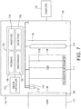
- FIG. 7 a block diagram illustrates an apparatus 700 according to an example embodiment.
- the apparatus 700 includes a device controller 702, which may include one or more processors, such as central processing units, subprocessors, digital signal processors, etc.
- the controller 702 is coupled to a memory 704 that includes functional modules that will be described in greater detail below.
- the memory 704 may include a combination of volatile and non-volatile memory, and may store instructions and data as known in the art.
- the apparatus includes an optical section 706 that includes an external interface 708 that receives light from outside the apparatus 700.
- the external interface 708 may include windows, lenses, filters, etc., suitable for passing light from outside the apparatus 700 to internal optical components.
- the interface 708 is configured to be coupled to an external lens 710.
- a polarization interferometer 712 is located in the optical section 706 of the apparatus 700.
- the polarization interferometer 712 is coupled to the controller 702, e.g., via electrical signal lines.
- the controller 702 applies signals to the polarization interferometer 712 to cause a time-varying optical path delay or retardance in an LCVR 712a that is part of the interferometer 712.
- This time-varying optical path delay creates an interferogram that varies as a function of the optical path delay.
- the interferogram is detected by an image sensor 714 (e.g., an array of sensor pixels or focal plane array) which is also coupled to the controller 702.
- the polarization interferometer 712 and LCVR 712a may be configured similar to previously described embodiments.
- a feedback sensor 716 and feedforward sensor 718 may be integrated with or attached to the LCVR 712a.
- the feedforward sensor 718 senses a state (e.g., temperature) of the LC cells within the LCVR 712a that may be incorporated into a feedforward control model.
- a feedback control module 720 uses signals produced via the feedback sensor 716 to control at least one LC cell of the LCVR 712a (e.g., a relatively thin LC cell).
- the feedback sensor 716 is a monochromatic light source on one side of the interferometer 712 and a photodetector on the other side of the interferometer 712, combined with signal processing to extract the retardance from the photodetector signal.
- the image sensor 714 may be used as part of the feedback sensor 716.
- the feedback sensor 716 could include circuitry that measures the capacitance of one or more of the LC cells within the interferometer 712. This capacitance signal can be converted to a retardance signal through a look-up table or other means.
- a feedforward control module 722 uses signals (e.g., temperature signals) produced via the feedforward sensor 718 as input to a feedforward control model used to control at least one other LC cell of the LCVR 712a (e.g., a relatively thick LC cell).
- the temperature adjusts an operating point of the feedforward control model, and an output of the model is used to modify a control input applied to one or more LC cells of the LCVR 712a.
- the control model used by the feedforward control module 722 may further be adjusted based on retardance errors detected by the feedback module 720.
- the output of the feedforward control model could be further adjusted to compensate for systematic deviations of a retardance trajectory of the LCVR 712a from a desired retardance trajectory.
- the feedback control module 720 is primarily using the thinner LC cell to compensate for short-time-scale, random (not systematic) deviations of retardance from a desired retardance trajectory.
- the polarization interferometer 712 may include an LC waveplate 712b that compensates for residual retardance of LC layers in the LCVR 712a.
- the LC waveplate 712b may be fixed or non-driven.
- the LC waveplate 712b may be driven by waveplate control module 724, which switches the LC waveplate 712b between first and second states having respective minimum and maximum retardance. These states may be discrete, e.g., no intermediate states, although the signals used to toggle between the discrete states may be varied based on local conditions, e.g., via feedback or feedforward adjustment.
- the apparatus 700 may be configured as a hyperspectral imager, where the relative path delay of portions of light passing through the polarization interferometer 712 is modified over a period of time. This path delay results in time- and position-dependent interferograms that are sensed at each pixel of the image sensor 714.
- the interferograms can be processed by performing an inverse cosine transform or Fourier transform of the recorded signal as a function of path delay, resulting in a hyperspectral data-cube. This processing may be performed by an image processing module 726. Some or all of the processing may be performed by an external device, such as computer 730 that is coupled to the apparatus 700 via a data transfer interface 728.
Landscapes
- Physics & Mathematics (AREA)
- Spectroscopy & Molecular Physics (AREA)
- General Physics & Mathematics (AREA)
- Nonlinear Science (AREA)
- Optics & Photonics (AREA)
- Crystallography & Structural Chemistry (AREA)
- Chemical & Material Sciences (AREA)
- Mathematical Physics (AREA)
- Engineering & Computer Science (AREA)
- Computer Hardware Design (AREA)
- Theoretical Computer Science (AREA)
- Liquid Crystal (AREA)
- Optical Modulation, Optical Deflection, Nonlinear Optics, Optical Demodulation, Optical Logic Elements (AREA)
- Spectrometry And Color Measurement (AREA)
Applications Claiming Priority (1)
| Application Number | Priority Date | Filing Date | Title |
|---|---|---|---|
| US15/827,204 US10564504B2 (en) | 2017-11-30 | 2017-11-30 | Liquid-crystal variable retarder using liquid crystal cells of differing thicknesses |
Publications (1)
| Publication Number | Publication Date |
|---|---|
| EP3492968A1 true EP3492968A1 (en) | 2019-06-05 |
Family
ID=64559620
Family Applications (1)
| Application Number | Title | Priority Date | Filing Date |
|---|---|---|---|
| EP18209312.0A Withdrawn EP3492968A1 (en) | 2017-11-30 | 2018-11-29 | Liquid-crystal variable retarder using liquid crystal cells of differing thicknesses |
Country Status (5)
| Country | Link |
|---|---|
| US (1) | US10564504B2 (enExample) |
| EP (1) | EP3492968A1 (enExample) |
| JP (1) | JP7073243B2 (enExample) |
| KR (1) | KR102430145B1 (enExample) |
| CN (1) | CN109856873A (enExample) |
Families Citing this family (8)
| Publication number | Priority date | Publication date | Assignee | Title |
|---|---|---|---|---|
| JP7267122B2 (ja) * | 2019-06-20 | 2023-05-01 | 日東電工株式会社 | 画像生成システム用光学フィルムのセット |
| CN110553730B (zh) * | 2019-09-09 | 2021-10-19 | 京东方科技集团股份有限公司 | 光谱仪 |
| KR20220136431A (ko) * | 2020-02-11 | 2022-10-07 | 밸브 코포레이션 | 고 충실도 표면 특성화 측정들을 위한 편광측정 카메라 |
| CN111323985A (zh) * | 2020-03-03 | 2020-06-23 | 中国科学院光电技术研究所 | 一种用于液晶光束偏转系统的控制器整定方法 |
| CN112859402B (zh) * | 2021-01-18 | 2022-09-09 | 北京理工大学重庆创新中心 | 一种液晶可变相位延迟器相位响应加速方法和加速系统 |
| CN113138467B (zh) * | 2021-04-15 | 2023-06-13 | 西北农林科技大学 | 一种基于lcvr的压缩感知高光谱偏振成像方法 |
| JP2023104136A (ja) * | 2022-01-17 | 2023-07-28 | シャープディスプレイテクノロジー株式会社 | 光学素子及び3次元表示装置 |
| US12436401B2 (en) * | 2023-01-31 | 2025-10-07 | Applied Materials Israel Ltd. | Polarization optical system |
Citations (4)
| Publication number | Priority date | Publication date | Assignee | Title |
|---|---|---|---|---|
| US20020181066A1 (en) * | 2000-08-31 | 2002-12-05 | Cambridge Research & Instrumentation, Inc., A Delaware Corporation | High performance polarization controller and polarization sensor |
| US6576886B1 (en) * | 2001-02-20 | 2003-06-10 | General Photonics Corporation | Dynamic control of polarization of an optical signal |
| US20140098309A1 (en) * | 2011-04-14 | 2014-04-10 | Chemlmage Corporation | Short-Wavelength Infrared (SWIR) Multi-Conjugate Liquid Crystal Tunable Filter |
| US20160123811A1 (en) | 2014-10-29 | 2016-05-05 | Palo Alto Research Center Incorporated | Liquid crystal fourier transform imaging spectrometer |
Family Cites Families (80)
| Publication number | Priority date | Publication date | Assignee | Title |
|---|---|---|---|---|
| US4342516A (en) | 1980-03-07 | 1982-08-03 | The Perkin-Elmer Corporation | Filter indexing for spectrophotometer system |
| US4461543A (en) * | 1982-03-26 | 1984-07-24 | Sperry Corporation | Electro optic switch |
| JPS62103529A (ja) | 1985-10-31 | 1987-05-14 | Toshiba Corp | 複合管 |
| US4848877A (en) | 1987-09-29 | 1989-07-18 | Cambridge Research And Instrumentation, Inc. | Liquid crystal devices and systems using such devices |
| US4905169A (en) | 1988-06-02 | 1990-02-27 | The United States Of America As Represented By The United States Department Of Energy | Method and apparatus for simultaneously measuring a plurality of spectral wavelengths present in electromagnetic radiation |
| US4979235A (en) * | 1989-04-17 | 1990-12-18 | Tektronix, Inc. | Polarization controller for use in optical fiber communication system |
| US5126869A (en) * | 1990-12-03 | 1992-06-30 | Raytheon Company | Two-dimensional, phased-array optical beam steerer |
| US5784162A (en) | 1993-08-18 | 1998-07-21 | Applied Spectral Imaging Ltd. | Spectral bio-imaging methods for biological research, medical diagnostics and therapy |
| US5247378A (en) | 1991-06-07 | 1993-09-21 | Peter Miller | Optical retarder having means for determining the retardance of the cell corresponding to the sensed capacitance thereof |
| DE69226998T2 (de) * | 1991-07-19 | 1999-04-15 | Sharp K.K., Osaka | Optisches Modulationselement und Vorrichtungen mit einem solchen Element |
| US5347382A (en) | 1992-04-23 | 1994-09-13 | Rumbaugh Scott H | Liquid crystal cell retarder with driving beyond retardance value and two cells for high speed |
| JPH0643449A (ja) * | 1992-07-27 | 1994-02-18 | Seikosha Co Ltd | 液晶光学装置 |
| JP2925064B2 (ja) * | 1993-12-02 | 1999-07-26 | 矢崎総業株式会社 | 可変波長フィルタ |
| JPH07212639A (ja) | 1994-01-25 | 1995-08-11 | Sony Corp | テレビジョン・カメラ用電子シャッター装置 |
| US5751384A (en) | 1995-05-23 | 1998-05-12 | The Board Of Regents Of The University Of Colorado | Color polarizers for polarizing an additive color spectrum along a first axis and it's compliment along a second axis |
| US5856842A (en) | 1996-08-26 | 1999-01-05 | Kaiser Optical Systems Corporation | Apparatus facilitating eye-contact video communications |
| EP1071977A2 (en) * | 1998-04-08 | 2001-01-31 | Corning Applied Technologies | High-speed electro-optic modulator |
| US6169594B1 (en) | 1998-08-24 | 2001-01-02 | Physical Optics Corporation | Beam deflector and scanner |
| EP1200796A1 (en) * | 1999-07-02 | 2002-05-02 | Cambridge Research & Instrumentation, Inc. | Birefringement interferometer |
| GB2354833A (en) | 1999-09-28 | 2001-04-04 | Sharp Lab Of Europ Ltd | Liquid crystal device |
| US7116370B1 (en) * | 2000-03-31 | 2006-10-03 | Sharp Laboratories Of Ameria, Inc. | Image processing system optical shifting mechanism |
| AU2001274937A1 (en) * | 2000-05-24 | 2001-12-03 | Purdue Research Foundation | Methods and systems for polarization control and polarization mode dispersion compensation for wideband optical signals |
| US7973936B2 (en) | 2001-01-30 | 2011-07-05 | Board Of Trustees Of Michigan State University | Control system and apparatus for use with ultra-fast laser |
| JP4382317B2 (ja) * | 2001-12-06 | 2009-12-09 | シチズンホールディングス株式会社 | 液晶可変波長フィルタ装置 |
| US6744509B2 (en) | 2002-08-20 | 2004-06-01 | Meadowlark Optics, Inc. | Retardance sweep polarimeter and method |
| US7067795B1 (en) * | 2002-10-03 | 2006-06-27 | General Photonics Corporation | Methods and systems for dynamic control of polarization of an optical signal |
| DE60209672T2 (de) * | 2002-10-15 | 2006-11-16 | Centre National De La Recherche Scientifique (C.N.R.S.) | Auf Flüssigkristallen basierendes polarimetrisches System, Verfahren zu seiner Kalibrierung, und polarimetrisches Messverfahren |
| CA2509909C (en) * | 2002-12-20 | 2011-05-24 | Fiso Technologies Inc. | Method and sensor for detecting a chemical substance using an optically anisotropic material |
| US7782377B2 (en) | 2003-02-26 | 2010-08-24 | Canon Kabushiki Kaisha | Image sensing apparatus, control method therefor, storage medium, and program to create correction data |
| JP4285350B2 (ja) | 2004-02-26 | 2009-06-24 | セイコーエプソン株式会社 | 視角制御素子およびその製造方法、液晶表示装置、電子機器 |
| JP2005348140A (ja) | 2004-06-03 | 2005-12-15 | Matsushita Electric Ind Co Ltd | カメラ装置 |
| US7522785B2 (en) * | 2004-12-01 | 2009-04-21 | General Photonics Corporation | Measurements of polarization-dependent loss (PDL) and degree of polarization (DOP) using optical polarization controllers |
| JP4400448B2 (ja) | 2004-12-22 | 2010-01-20 | コニカミノルタセンシング株式会社 | 分光輝度計の校正方法、及び校正システムの動作プログラム |
| US6992809B1 (en) * | 2005-02-02 | 2006-01-31 | Chemimage Corporation | Multi-conjugate liquid crystal tunable filter |
| EP1875202A1 (en) | 2005-03-29 | 2008-01-09 | Yoel Arieli | Spectral imaging camera and applications |
| US7420663B2 (en) | 2005-05-24 | 2008-09-02 | Bwt Property Inc. | Spectroscopic sensor on mobile phone |
| JP4684771B2 (ja) | 2005-06-30 | 2011-05-18 | Hoya株式会社 | 像振れ補正装置 |
| JP4205704B2 (ja) * | 2005-08-02 | 2009-01-07 | 国立大学法人 北海道大学 | 撮像偏光計測方法 |
| US7639363B2 (en) * | 2005-09-07 | 2009-12-29 | California Institute Of Technology | Electro-optic imaging Fourier transform spectrometer |
| US7630022B1 (en) * | 2005-09-20 | 2009-12-08 | Thomas Baur | Advanced liquid crystal tunable filters and method |
| US7336323B2 (en) * | 2005-09-27 | 2008-02-26 | Chemimage Corporation | Liquid crystal filter with tunable rejection band |
| US7525712B2 (en) * | 2005-09-29 | 2009-04-28 | Teledyne Scientific & Imaging, Llc | Broad spectral range polarization rotator |
| DE102005048240A1 (de) | 2005-10-07 | 2007-04-19 | Stefan Steib | Verfahren zur spektralen, integrierten Kalibrierung eines Bildsensors mittels monochromatischer Lichtquellen |
| US8081311B2 (en) | 2005-11-04 | 2011-12-20 | General Hospital Corporation | System for multispectral imaging |
| US8644911B1 (en) | 2006-06-30 | 2014-02-04 | Hypermed Imaging, Inc. | OxyVu-1 hyperspectral tissue oxygenation (HTO) measurement system |
| US8447087B2 (en) | 2006-09-12 | 2013-05-21 | Carestream Health, Inc. | Apparatus and method for caries detection |
| WO2008068753A2 (en) * | 2006-12-04 | 2008-06-12 | Ben-Gurion University Of The Negev - Research And Development Authority | Polarization independent birefringent tunable filters |
| GB0717967D0 (en) | 2007-09-14 | 2007-10-24 | Cascade Technologies Ltd | Polarimetric hyperspectral imager |
| EP2265936A2 (en) | 2008-04-01 | 2010-12-29 | Koninklijke Philips Electronics N.V. | Spectral detector calibration |
| US8406859B2 (en) | 2008-08-10 | 2013-03-26 | Board Of Regents, The University Of Texas System | Digital light processing hyperspectral imaging apparatus |
| AU2010203357B2 (en) | 2009-01-10 | 2014-07-10 | Carne Tender, Llc | System and method for analyzing properties of meat using multispectral imaging |
| JP5278159B2 (ja) * | 2009-05-20 | 2013-09-04 | 富士通株式会社 | 偏波コントローラおよび偏波モード分散補償器 |
| US8525970B2 (en) * | 2009-05-21 | 2013-09-03 | The Hong Kong University Of Science And Technology | Photo-aligned liquid-crystal micropolarimeter array and its manufacturing method |
| US8982313B2 (en) * | 2009-07-31 | 2015-03-17 | North Carolina State University | Beam steering devices including stacked liquid crystal polarization gratings and related methods of operation |
| US7999933B2 (en) | 2009-08-14 | 2011-08-16 | Princeton Instruments | Method for calibrating imaging spectrographs |
| US8400574B2 (en) * | 2010-04-16 | 2013-03-19 | Chemimage Corporation | Short wave infrared multi-conjugate liquid crystal tunable filter |
| WO2011132455A1 (ja) | 2010-04-19 | 2011-10-27 | シャープ株式会社 | 表示装置 |
| US20110299089A1 (en) | 2010-06-04 | 2011-12-08 | University Of Washington | Compact liquid crystal based fourier transform spectrometer system |
| US20120013922A1 (en) | 2010-07-19 | 2012-01-19 | Lotz Michael G | Print Data Format Modification Mechanism |
| US9046422B2 (en) | 2011-04-20 | 2015-06-02 | The Arizona Board Of Regents On Behalf Of The University Of Arizona | Ultra-compact snapshot imaging fourier transform spectrometer |
| US8422119B1 (en) | 2010-09-20 | 2013-04-16 | Disco Corporation | Compensation of beam walkoff in nonlinear crystal using cylindrical lens |
| US8736777B2 (en) * | 2011-01-19 | 2014-05-27 | Chemimage Technologies Llc | VIS-SNIR multi-conjugate liquid crystal tunable filter |
| EP2551635A1 (de) | 2011-07-26 | 2013-01-30 | Hexagon Technology Center GmbH | Optisches Messsystem mit Filtereinheit zur Extraktion elektromagnetischer Strahlung |
| EP2736411A4 (en) | 2011-07-28 | 2015-07-01 | Massachusetts Inst Technology | CAMERA CONFIGURATION FOR THE THREE-DIMENSIONAL ILLUSTRATION OF INDOOR SPACES |
| JP2013096883A (ja) | 2011-11-02 | 2013-05-20 | Seiko Epson Corp | 分光測定装置 |
| US20140362331A1 (en) * | 2013-03-15 | 2014-12-11 | Chemlmage Corporation | Short-Wavelength Infrared (SWIR) Multi-Conjugate Liquid Crystal Tunable Filter |
| US20140354868A1 (en) * | 2013-06-04 | 2014-12-04 | Corning Incorporated | Portable hyperspectral imager |
| US9513166B2 (en) | 2013-07-16 | 2016-12-06 | Utah State University Research Foundation | Split field spectral imager |
| WO2015015722A1 (ja) * | 2013-07-29 | 2015-02-05 | パナソニックIpマネジメント株式会社 | 光学フィルタおよびそれを用いた偏光撮像装置 |
| US9631973B2 (en) | 2013-12-13 | 2017-04-25 | Raytheon Company | Multifunction imager |
| CN106462017B (zh) * | 2014-04-02 | 2019-08-09 | 依视路国际公司 | 消色差相位调制器和光学器件 |
| US11490037B2 (en) | 2014-10-29 | 2022-11-01 | Palo Alto Research Center Incorporated | Liquid crystal fourier transform imaging spectrometer |
| US10469771B2 (en) * | 2014-10-29 | 2019-11-05 | Palo Alto Research Center Incorporated | Liquid crystal fourier transform imaging spectrometer |
| WO2016075694A1 (en) * | 2014-11-16 | 2016-05-19 | B.G. Negev Technologies & Applications Ltd. At Ben-Gurion University | Multi-spectral polarimetric variable optical device and imager |
| EP3243103B1 (en) * | 2015-01-09 | 2020-04-29 | Essilor International | Liquid-crystal achromatic phase modulator |
| US10228517B2 (en) * | 2015-03-03 | 2019-03-12 | Nistica, Inc. | Optical arrangement for managing diversity and isolation between ports in a wavelength selective switch |
| WO2018067212A2 (en) * | 2016-06-20 | 2018-04-12 | Massachusetts Institute Of Technology | Methods and systems for time-encoded multiplexed imaging |
| US10768497B2 (en) * | 2016-10-03 | 2020-09-08 | Xerox Corporation | Hyperspectral imaging system |
| US20190324212A1 (en) * | 2017-01-06 | 2019-10-24 | Molex, Llc | Optical arrangement for suppressing outerband crosstalk in a wavelength selective switch |
| US10884278B2 (en) * | 2017-10-24 | 2021-01-05 | Palo Alto Research Center Incorporated | Liquid crystal temperature control by resistive heating |
-
2017
- 2017-11-30 US US15/827,204 patent/US10564504B2/en not_active Expired - Fee Related
-
2018
- 2018-11-05 JP JP2018207826A patent/JP7073243B2/ja not_active Expired - Fee Related
- 2018-11-06 CN CN201811311279.XA patent/CN109856873A/zh active Pending
- 2018-11-15 KR KR1020180140499A patent/KR102430145B1/ko active Active
- 2018-11-29 EP EP18209312.0A patent/EP3492968A1/en not_active Withdrawn
Patent Citations (4)
| Publication number | Priority date | Publication date | Assignee | Title |
|---|---|---|---|---|
| US20020181066A1 (en) * | 2000-08-31 | 2002-12-05 | Cambridge Research & Instrumentation, Inc., A Delaware Corporation | High performance polarization controller and polarization sensor |
| US6576886B1 (en) * | 2001-02-20 | 2003-06-10 | General Photonics Corporation | Dynamic control of polarization of an optical signal |
| US20140098309A1 (en) * | 2011-04-14 | 2014-04-10 | Chemlmage Corporation | Short-Wavelength Infrared (SWIR) Multi-Conjugate Liquid Crystal Tunable Filter |
| US20160123811A1 (en) | 2014-10-29 | 2016-05-05 | Palo Alto Research Center Incorporated | Liquid crystal fourier transform imaging spectrometer |
Also Published As
| Publication number | Publication date |
|---|---|
| JP7073243B2 (ja) | 2022-05-23 |
| KR102430145B1 (ko) | 2022-08-08 |
| KR20190064443A (ko) | 2019-06-10 |
| CN109856873A (zh) | 2019-06-07 |
| JP2019101416A (ja) | 2019-06-24 |
| US20190162999A1 (en) | 2019-05-30 |
| US10564504B2 (en) | 2020-02-18 |
Similar Documents
| Publication | Publication Date | Title |
|---|---|---|
| US10564504B2 (en) | Liquid-crystal variable retarder using liquid crystal cells of differing thicknesses | |
| JP6702689B2 (ja) | 液晶のフーリエ変換撮像分光器 | |
| US10334186B2 (en) | Liquid crystal fourier transform imaging spectrometer | |
| US10768497B2 (en) | Hyperspectral imaging system | |
| US10469771B2 (en) | Liquid crystal fourier transform imaging spectrometer | |
| WO2012111570A1 (ja) | 空間光変調装置および空間光変調方法 | |
| US20060227402A1 (en) | Wavefront correction system | |
| JP7082564B2 (ja) | 均一または不均一にサンプリングされたインターフェログラムを変換してスペクトルデータを生成する方法および装置 | |
| CN109991768B (zh) | 用于在液晶可变滞后器上分布光的出瞳扩大器 | |
| AU2014289101B2 (en) | Device for compensating for the drift of a phase shift of a device for modulating the polarization state of a light beam | |
| CN112525493A (zh) | 一种铁电液晶延迟器光学特性检测方法及装置 | |
| Gendre et al. | Full Stokes polarimetric imaging using a single ferroelectric liquid crystal device | |
| EP3505889A1 (en) | Measuring path delay through a liquid-crystal variable retarder at non-uniform retardance intervals | |
| CN120628294A (zh) | 基于液晶可变相位延迟器的可见光宽谱段偏振成像系统及成像方法 | |
| Peinado et al. | Design of a polarimeter with two ferroelectric liquid crystal panels |
Legal Events
| Date | Code | Title | Description |
|---|---|---|---|
| PUAI | Public reference made under article 153(3) epc to a published international application that has entered the european phase |
Free format text: ORIGINAL CODE: 0009012 |
|
| STAA | Information on the status of an ep patent application or granted ep patent |
Free format text: STATUS: THE APPLICATION HAS BEEN PUBLISHED |
|
| AK | Designated contracting states |
Kind code of ref document: A1 Designated state(s): AL AT BE BG CH CY CZ DE DK EE ES FI FR GB GR HR HU IE IS IT LI LT LU LV MC MK MT NL NO PL PT RO RS SE SI SK SM TR |
|
| AX | Request for extension of the european patent |
Extension state: BA ME |
|
| STAA | Information on the status of an ep patent application or granted ep patent |
Free format text: STATUS: REQUEST FOR EXAMINATION WAS MADE |
|
| 17P | Request for examination filed |
Effective date: 20191205 |
|
| RBV | Designated contracting states (corrected) |
Designated state(s): AL AT BE BG CH CY CZ DE DK EE ES FI FR GB GR HR HU IE IS IT LI LT LU LV MC MK MT NL NO PL PT RO RS SE SI SK SM TR |
|
| STAA | Information on the status of an ep patent application or granted ep patent |
Free format text: STATUS: EXAMINATION IS IN PROGRESS |
|
| 17Q | First examination report despatched |
Effective date: 20210721 |
|
| GRAP | Despatch of communication of intention to grant a patent |
Free format text: ORIGINAL CODE: EPIDOSNIGR1 |
|
| STAA | Information on the status of an ep patent application or granted ep patent |
Free format text: STATUS: GRANT OF PATENT IS INTENDED |
|
| RIC1 | Information provided on ipc code assigned before grant |
Ipc: H04N 5/33 20060101ALN20230714BHEP Ipc: H04N 5/30 20060101ALN20230714BHEP Ipc: G01J 3/453 20060101ALN20230714BHEP Ipc: G01J 3/45 20060101ALN20230714BHEP Ipc: G01J 3/447 20060101ALN20230714BHEP Ipc: G01J 3/28 20060101ALN20230714BHEP Ipc: G05B 13/00 20060101ALN20230714BHEP Ipc: G05B 11/00 20060101ALN20230714BHEP Ipc: G05B 6/00 20060101ALN20230714BHEP Ipc: G02B 27/28 20060101ALN20230714BHEP Ipc: G02B 27/00 20060101ALN20230714BHEP Ipc: G02B 5/30 20060101ALN20230714BHEP Ipc: G02F 1/133 20060101AFI20230714BHEP |
|
| RIC1 | Information provided on ipc code assigned before grant |
Ipc: H04N 5/33 20060101ALN20230801BHEP Ipc: H04N 5/30 20060101ALN20230801BHEP Ipc: G01J 3/453 20060101ALN20230801BHEP Ipc: G01J 3/45 20060101ALN20230801BHEP Ipc: G01J 3/447 20060101ALN20230801BHEP Ipc: G01J 3/28 20060101ALN20230801BHEP Ipc: G05B 13/00 20060101ALN20230801BHEP Ipc: G05B 11/00 20060101ALN20230801BHEP Ipc: G05B 6/00 20060101ALN20230801BHEP Ipc: G02B 27/28 20060101ALN20230801BHEP Ipc: G02B 27/00 20060101ALN20230801BHEP Ipc: G02B 5/30 20060101ALN20230801BHEP Ipc: G02F 1/133 20060101AFI20230801BHEP |
|
| INTG | Intention to grant announced |
Effective date: 20230822 |
|
| RIN1 | Information on inventor provided before grant (corrected) |
Inventor name: HEGYI, ALEX |
|
| STAA | Information on the status of an ep patent application or granted ep patent |
Free format text: STATUS: THE APPLICATION IS DEEMED TO BE WITHDRAWN |
|
| 18D | Application deemed to be withdrawn |
Effective date: 20240103 |