EP3489395A1 - Metal electrodeposition cathode plate and production method therefor - Google Patents
Metal electrodeposition cathode plate and production method therefor Download PDFInfo
- Publication number
- EP3489395A1 EP3489395A1 EP17830882.1A EP17830882A EP3489395A1 EP 3489395 A1 EP3489395 A1 EP 3489395A1 EP 17830882 A EP17830882 A EP 17830882A EP 3489395 A1 EP3489395 A1 EP 3489395A1
- Authority
- EP
- European Patent Office
- Prior art keywords
- conductive film
- cathode plate
- nickel
- protrusion
- plate
- Prior art date
- Legal status (The legal status is an assumption and is not a legal conclusion. Google has not performed a legal analysis and makes no representation as to the accuracy of the status listed.)
- Withdrawn
Links
- 229910052751 metal Inorganic materials 0.000 title claims abstract description 104
- 239000002184 metal Substances 0.000 title claims abstract description 104
- 238000004070 electrodeposition Methods 0.000 title claims abstract description 40
- 238000004519 manufacturing process Methods 0.000 title claims abstract description 20
- PXHVJJICTQNCMI-UHFFFAOYSA-N Nickel Chemical compound [Ni] PXHVJJICTQNCMI-UHFFFAOYSA-N 0.000 claims description 186
- 229910052759 nickel Inorganic materials 0.000 claims description 93
- 239000010935 stainless steel Substances 0.000 claims description 10
- 229910001220 stainless steel Inorganic materials 0.000 claims description 10
- RTAQQCXQSZGOHL-UHFFFAOYSA-N Titanium Chemical compound [Ti] RTAQQCXQSZGOHL-UHFFFAOYSA-N 0.000 claims description 8
- 239000010936 titanium Substances 0.000 claims description 8
- 238000007747 plating Methods 0.000 claims description 6
- 229910001200 Ferrotitanium Inorganic materials 0.000 claims description 3
- 229920005989 resin Polymers 0.000 description 19
- 239000011347 resin Substances 0.000 description 19
- 238000007650 screen-printing Methods 0.000 description 12
- 238000000034 method Methods 0.000 description 10
- 230000000052 comparative effect Effects 0.000 description 9
- 230000007423 decrease Effects 0.000 description 7
- 238000006073 displacement reaction Methods 0.000 description 7
- 239000008151 electrolyte solution Substances 0.000 description 7
- 238000005530 etching Methods 0.000 description 6
- 229920001187 thermosetting polymer Polymers 0.000 description 6
- 239000011248 coating agent Substances 0.000 description 5
- 238000000576 coating method Methods 0.000 description 5
- 238000012545 processing Methods 0.000 description 5
- 229910052719 titanium Inorganic materials 0.000 description 5
- 238000005868 electrolysis reaction Methods 0.000 description 4
- 238000012423 maintenance Methods 0.000 description 4
- 239000000463 material Substances 0.000 description 4
- 238000001039 wet etching Methods 0.000 description 4
- 238000011161 development Methods 0.000 description 3
- 239000003822 epoxy resin Substances 0.000 description 3
- 238000010438 heat treatment Methods 0.000 description 3
- 230000002093 peripheral effect Effects 0.000 description 3
- 238000000016 photochemical curing Methods 0.000 description 3
- 229920000647 polyepoxide Polymers 0.000 description 3
- 230000003746 surface roughness Effects 0.000 description 3
- 230000015572 biosynthetic process Effects 0.000 description 2
- 238000005260 corrosion Methods 0.000 description 2
- 230000007797 corrosion Effects 0.000 description 2
- 238000001723 curing Methods 0.000 description 2
- 239000002659 electrodeposit Substances 0.000 description 2
- 238000011156 evaluation Methods 0.000 description 2
- 238000013007 heat curing Methods 0.000 description 2
- 238000001746 injection moulding Methods 0.000 description 2
- 239000002994 raw material Substances 0.000 description 2
- 239000000243 solution Substances 0.000 description 2
- VYZAMTAEIAYCRO-UHFFFAOYSA-N Chromium Chemical compound [Cr] VYZAMTAEIAYCRO-UHFFFAOYSA-N 0.000 description 1
- 239000004593 Epoxy Substances 0.000 description 1
- 229910021578 Iron(III) chloride Inorganic materials 0.000 description 1
- 229910021586 Nickel(II) chloride Inorganic materials 0.000 description 1
- ISWSIDIOOBJBQZ-UHFFFAOYSA-N Phenol Chemical compound OC1=CC=CC=C1 ISWSIDIOOBJBQZ-UHFFFAOYSA-N 0.000 description 1
- 239000004642 Polyimide Substances 0.000 description 1
- BQCADISMDOOEFD-UHFFFAOYSA-N Silver Chemical compound [Ag] BQCADISMDOOEFD-UHFFFAOYSA-N 0.000 description 1
- ATJFFYVFTNAWJD-UHFFFAOYSA-N Tin Chemical compound [Sn] ATJFFYVFTNAWJD-UHFFFAOYSA-N 0.000 description 1
- HCHKCACWOHOZIP-UHFFFAOYSA-N Zinc Chemical compound [Zn] HCHKCACWOHOZIP-UHFFFAOYSA-N 0.000 description 1
- 230000001070 adhesive effect Effects 0.000 description 1
- 229910045601 alloy Inorganic materials 0.000 description 1
- 239000000956 alloy Substances 0.000 description 1
- 238000006243 chemical reaction Methods 0.000 description 1
- 229910052804 chromium Inorganic materials 0.000 description 1
- 239000011651 chromium Substances 0.000 description 1
- 229910017052 cobalt Inorganic materials 0.000 description 1
- 239000010941 cobalt Substances 0.000 description 1
- GUTLYIVDDKVIGB-UHFFFAOYSA-N cobalt atom Chemical compound [Co] GUTLYIVDDKVIGB-UHFFFAOYSA-N 0.000 description 1
- 238000005520 cutting process Methods 0.000 description 1
- 230000002950 deficient Effects 0.000 description 1
- 230000000694 effects Effects 0.000 description 1
- 239000011521 glass Substances 0.000 description 1
- PCHJSUWPFVWCPO-UHFFFAOYSA-N gold Chemical compound [Au] PCHJSUWPFVWCPO-UHFFFAOYSA-N 0.000 description 1
- 229910052737 gold Inorganic materials 0.000 description 1
- 239000010931 gold Substances 0.000 description 1
- 238000009413 insulation Methods 0.000 description 1
- 238000011835 investigation Methods 0.000 description 1
- RBTARNINKXHZNM-UHFFFAOYSA-K iron trichloride Chemical compound Cl[Fe](Cl)Cl RBTARNINKXHZNM-UHFFFAOYSA-K 0.000 description 1
- QMMRZOWCJAIUJA-UHFFFAOYSA-L nickel dichloride Chemical compound Cl[Ni]Cl QMMRZOWCJAIUJA-UHFFFAOYSA-L 0.000 description 1
- 230000035515 penetration Effects 0.000 description 1
- 229920002647 polyamide Polymers 0.000 description 1
- 229920001721 polyimide Polymers 0.000 description 1
- 230000001376 precipitating effect Effects 0.000 description 1
- 238000003672 processing method Methods 0.000 description 1
- 238000005488 sandblasting Methods 0.000 description 1
- 229910052709 silver Inorganic materials 0.000 description 1
- 239000004332 silver Substances 0.000 description 1
- 229910052718 tin Inorganic materials 0.000 description 1
- 239000011135 tin Substances 0.000 description 1
- 229910052725 zinc Inorganic materials 0.000 description 1
- 239000011701 zinc Substances 0.000 description 1
Images



Classifications
-
- C—CHEMISTRY; METALLURGY
- C25—ELECTROLYTIC OR ELECTROPHORETIC PROCESSES; APPARATUS THEREFOR
- C25C—PROCESSES FOR THE ELECTROLYTIC PRODUCTION, RECOVERY OR REFINING OF METALS; APPARATUS THEREFOR
- C25C1/00—Electrolytic production, recovery or refining of metals by electrolysis of solutions
- C25C1/06—Electrolytic production, recovery or refining of metals by electrolysis of solutions or iron group metals, refractory metals or manganese
- C25C1/08—Electrolytic production, recovery or refining of metals by electrolysis of solutions or iron group metals, refractory metals or manganese of nickel or cobalt
-
- C—CHEMISTRY; METALLURGY
- C25—ELECTROLYTIC OR ELECTROPHORETIC PROCESSES; APPARATUS THEREFOR
- C25C—PROCESSES FOR THE ELECTROLYTIC PRODUCTION, RECOVERY OR REFINING OF METALS; APPARATUS THEREFOR
- C25C7/00—Constructional parts, or assemblies thereof, of cells; Servicing or operating of cells
- C25C7/02—Electrodes; Connections thereof
-
- C—CHEMISTRY; METALLURGY
- C25—ELECTROLYTIC OR ELECTROPHORETIC PROCESSES; APPARATUS THEREFOR
- C25C—PROCESSES FOR THE ELECTROLYTIC PRODUCTION, RECOVERY OR REFINING OF METALS; APPARATUS THEREFOR
- C25C7/00—Constructional parts, or assemblies thereof, of cells; Servicing or operating of cells
- C25C7/06—Operating or servicing
- C25C7/08—Separating of deposited metals from the cathode
-
- C—CHEMISTRY; METALLURGY
- C25—ELECTROLYTIC OR ELECTROPHORETIC PROCESSES; APPARATUS THEREFOR
- C25D—PROCESSES FOR THE ELECTROLYTIC OR ELECTROPHORETIC PRODUCTION OF COATINGS; ELECTROFORMING; APPARATUS THEREFOR
- C25D1/00—Electroforming
- C25D1/003—3D structures, e.g. superposed patterned layers
-
- C—CHEMISTRY; METALLURGY
- C25—ELECTROLYTIC OR ELECTROPHORETIC PROCESSES; APPARATUS THEREFOR
- C25D—PROCESSES FOR THE ELECTROLYTIC OR ELECTROPHORETIC PRODUCTION OF COATINGS; ELECTROFORMING; APPARATUS THEREFOR
- C25D1/00—Electroforming
- C25D1/20—Separation of the formed objects from the electrodes with no destruction of said electrodes
-
- C—CHEMISTRY; METALLURGY
- C25—ELECTROLYTIC OR ELECTROPHORETIC PROCESSES; APPARATUS THEREFOR
- C25D—PROCESSES FOR THE ELECTROLYTIC OR ELECTROPHORETIC PRODUCTION OF COATINGS; ELECTROFORMING; APPARATUS THEREFOR
- C25D17/00—Constructional parts, or assemblies thereof, of cells for electrolytic coating
- C25D17/10—Electrodes, e.g. composition, counter electrode
- C25D17/12—Shape or form
-
- C—CHEMISTRY; METALLURGY
- C25—ELECTROLYTIC OR ELECTROPHORETIC PROCESSES; APPARATUS THEREFOR
- C25D—PROCESSES FOR THE ELECTROLYTIC OR ELECTROPHORETIC PRODUCTION OF COATINGS; ELECTROFORMING; APPARATUS THEREFOR
- C25D17/00—Constructional parts, or assemblies thereof, of cells for electrolytic coating
- C25D17/16—Apparatus for electrolytic coating of small objects in bulk
Definitions
- Fig. 5 is a view illustrating an example of a conventional cathode plate to be used in production of blobby electric nickel.
- a cathode plate 11 is masked with a non-conductive film 13 on a flat plate-shaped metal plate 12 except the place to be a conductive portion 12a, and the conductive portion 12a is a concave portion and the non-conductive film 13 is a convex portion on this cathode plate 11.
- Nickel having a proper size is electrodeposited on the conductive portion 12a and blobby electric nickel is thus produced by using such a cathode plate 11.
- the nickel 14 begins to be electrodeposited and precipitated from the conductive portion 12a, grows not only in the thickness (longitudinal) direction but also in the planar (lateral) direction, and is in the state of being piled on the upper portion of the non-conductive film 13 as well.
- the non-conductive film (non-conductive portion) to be formed on the cathode plate has a long service life and can be easily maintained even in the case of being lost (deteriorated).
- the nickel 14 begins to be electrodeposited and precipitated from the conductive portion 12a, grows not only in the longitudinal direction but also in the lateral direction, and thus is in the state of gradually being piled on the non-conductive film 13 as well when blobby electric nickel is produced by using the cathode plate 11 as illustrated in Fig. 5 and Fig. 6 .
- the part of the thin non-conductive film 13 to be formed in the vicinity of the boundary with the conductive portion 12a is likely to be lost by the stress at the time of electrodeposition of the nickel 14 and the impact at the time of peeling off of the electric nickel as well as the adhesive property of the part with the metal plate 12 is likely to diminish by penetration of the electrolytic solution.
- an object of the present invention is to provide a metal electrodeposition cathode plate in which a non-conductive film on a metal plate is hardly lost and which can be repeatedly used and a production method therefor.
- the inventors of the present invention have carried out intensive investigations in order to solve the problems described above. As a result, it has been found out that the non-conductive film is hardly lost as protrusions are provided on a metal plate to form a conductive portion and a non-conductive film is provided on the metal surface except the protrusions, whereby the present invention has been completed.
- the present invention it is possible to provide a metal electrodeposition cathode plate in which a non-conductive film is hardly lost and which can be repeatedly used and a production method therefor.
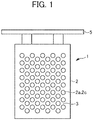
- a cathode plate 1 includes a metal plate 2 on which a plurality of disc-shaped protrusions 2a is disposed and a non-conductive film 3 formed on the surface of the metal plate 2 except the protrusions 2a as illustrated in Fig. 1 .
- the cathode plate 1 is used, for example, by being hung in an electrolytic cell containing an electrolytic solution containing nickel and an anode by a hanging member 5 and nickel having a desired shape is electrodeposited and precipitated on the surface of the cathode plate as to be described later.
- the material for the metal plate 2 is not particularly limited as long as it is a metal which is less susceptible to corrosion by the electrolytic solution to be used and forms only loose bonding with an electrodeposit such as nickel, but preferred examples thereof may include titanium and stainless steel.
- the non-conductive film 3 is formed on the flat area 2b having a concave step formed by the adjacent protrusions 2a and thus the non-conductive film 3 having a predetermined thickness is formed.
- the minimum film thickness Y of the non-conductive film 3 is the same as or greater than the height X of the protrusion 2a and it is preferably the same as the height X.
- the impact to be applied to the end portion of the non-conductive film 3 by the nickel 4 is minor and the non-conductive film 3 is hardly lost even when the nickel 4 is peeled off from the cathode plate 1.
- the non-conductive film 3 is hardly lost and it is thus possible to repeatedly use the non-conductive film 3 in electrodeposition without replacing the non-conductive film 3, to decrease the maintenance cost, and to achieve improvement in the productivity.
- a plurality of pieces of blobby electric nickel can be obtained from one cathode plate 1 by peeling off the nickel 4 from the cathode plate 1 after the electrodeposition of nickel is terminated.
- the non-conductive film 3 is hardly lost and it is thus possible to repeatedly use the non-conductive film 3 without replacing the non-conductive film 3, to decrease the maintenance cost, and to achieve improvement in the productivity.
- a plurality of disc-shaped protrusions 2a is formed on the surface of the metal plate 2.
- the parts of the flat plate-shaped metal plate 2 except the protrusions 2a are scraped, the protrusions 2a having a height X are left, and flat areas 2b are thus formed.
- the processing method is not particularly limited, and the formation of flat areas 2b can be conducted by, for example, wet etching processing, end mill processing, and laser processing.
- the protrusions 2a may be formed only on one surface of the metal plate 2 or on both surfaces of the metal plate 2.
- the non-conductive film 3 is formed on the flat areas 2b to be the surface of the metal plate 2 except the protrusions 2a.
- the method for forming the non-conductive film 3 is not particularly limited, and the formation of the non-conductive film 3 can be conducted by screen printing. In a case in which the material for the non-conductive film 3 is a thermosetting resin or a photocurable resin, heat curing or photocuring may be conducted if necessary.
- a cathode plate was fabricated in the same manner as in Example 1 except that the height X of the protrusion of the metal plate was set to 500 ⁇ m and the non-conductive film was formed on the flat area so as to have a predetermined thickness.
- the difference between the minimum film thickness of the non-conductive film and the height of the protrusion was measured at arbitrary 10 places by using a laser displacement meter, and the results were in a range of from -200 to -150 ⁇ m and the minimum film thickness Y of the non-conductive film 3 was thus 300 ⁇ m.
- the minimum film thickness Y of the non-conductive film 3 is thinner than 500 ⁇ m of the height of the protrusion.
- Nickel electrodeposited at the adjacent protrusions and conductive portions are connected to each other and electric nickel having a desired shape cannot be obtained in some cases when the loss of the non-conductive film expands.
- the use was stopped and the number of repetitions up to this time point was evaluated in a case in which the non-conductive film was lost from the boundary with the protrusion in the direction of the flat area by 1 mm or more.
- the use was stopped and the number of repetitions up to this time point was evaluated in a case in which the non-conductive film was lost and the diameter of the conductive portion increased by 1 mm or more as well.
Landscapes
- Chemical & Material Sciences (AREA)
- Engineering & Computer Science (AREA)
- Chemical Kinetics & Catalysis (AREA)
- Electrochemistry (AREA)
- Materials Engineering (AREA)
- Metallurgy (AREA)
- Organic Chemistry (AREA)
- Crystallography & Structural Chemistry (AREA)
- Electrolytic Production Of Metals (AREA)
Abstract

Description
- The present invention relates to a metal electrodeposition cathode plate and a production method therefor.
- Conventionally, electric nickel serving as an anode raw material for nickel plating has been used by being placed in a titanium basket to be an anode holding tool and hung in a nickel plating tank. At this time, as the electric nickel of an anode raw material, those obtained by cutting plate-shaped electric nickel electrodeposited on a cathode plate into small pieces have been used.
- However, the corner of the small pieces of electric nickel is sharp, and it has been thus difficult to handle the electric nickel when charging the electric nickel into a titanium basket. In addition, the small pieces of electric nickel cause so-called scaffold bridging as the corner thereof is caught by the mesh of the titanium basket after the electric nickel was charged in the titanium basket, the filling state of electric nickel in the titanium basket changes, and this causes plating unevenness in some cases.
- Hence, it has been proposed to use blobby (button-shaped) electric nickel with rounded corner. The blobby electric nickel can be produced, for example, by precipitating nickel on a conductive portion by using a cathode plate on which a plurality of circular conductive portions is disposed at regular intervals by electrolysis and then peeling off the electrodeposited nickel from the conductive portion. According to such a method, it is possible to efficiently produce a plurality of pieces of blobby electric nickel from one cathode plate.
-
Fig. 5 is a view illustrating an example of a conventional cathode plate to be used in production of blobby electric nickel. Acathode plate 11 is masked with anon-conductive film 13 on a flat plate-shaped metal plate 12 except the place to be aconductive portion 12a, and theconductive portion 12a is a concave portion and thenon-conductive film 13 is a convex portion on thiscathode plate 11. Nickel having a proper size is electrodeposited on theconductive portion 12a and blobby electric nickel is thus produced by using such acathode plate 11. - As a method for forming the
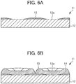
non-conductive film 13 on themetal plate 12 as thecathode plate 11, for example, there is a method for forming anon-conductive film 13 having a desired pattern by coating a thermosetting non-conductive resin such as an epoxy resin on the flat plate-shaped metal plate 12 by a screen printing method and heating the thermosetting non-conductive resin as illustrated inFig. 6A (seePatent Documents 1 and 2). Incidentally,Fig. 6B illustrates a state in which nickel (electric nickel) 14 is electrodeposited and precipitated on theconductive portion 12a by using thecathode plate 11 on which thenon-conductive film 13 is formed. In thecathode plate 11, thenickel 14 begins to be electrodeposited and precipitated from theconductive portion 12a, grows not only in the thickness (longitudinal) direction but also in the planar (lateral) direction, and is in the state of being piled on the upper portion of thenon-conductive film 13 as well. - In addition, for example, there has also been proposed a method for forming a
non-conductive film 23 having a desired pattern by coating a photosensitive non-conductive resin on ametal plate 22 and removing the non-conductive resin at the place corresponding to aconductive portion 22a by exposure and development as illustrated inFig. 7A . Incidentally,Fig. 7B illustrates a state in which nickel (electric nickel) 24 is electrodeposited and precipitated on theconductive portion 22a by using thecathode plate 21 on which thenon-conductive film 23 is formed. In thecathode plate 21 as well, thenickel 24 begins to be electrodeposited and precipitated from theconductive portion 22a and grows not only in the thickness direction but also in the planar direction. - Furthermore, there has also been proposed a method for producing a cathode plate constituting a non-conductive portion by solidifying the periphery of a metal structure incorporated so that a plurality of studs to be a conductive portion is disposed at regular intervals with an insulating resin by an injection molding method (see Patent Document 3).
- Patent Document 1: Japanese Examined Patent Application Publication No.
S51-036693 - Patent Document 2: Japanese Unexamined Patent Application, Publication No.
S52-152832 - Patent Document 3: Japanese Examined Patent Application Publication No.
S56-029960 - Meanwhile, in a case in which blobby electric nickel is produced using a cathode plate as described above, it is required that the non-conductive film (non-conductive portion) to be formed on the cathode plate has a long service life and can be easily maintained even in the case of being lost (deteriorated).
- The film thickness of the
non-conductive film 13 gradually decreases toward theconductive portion 12a and is thus significantly thin at the boundary with theconductive portion 12a in a case in which thenon-conductive film 13 is formed by coating a non-conductive resin on themetal plate 12 by screen printing as illustrated inFig. 6A . Such a change in the film thickness of thenon-conductive film 13 depends on the amount of the non-conductive resin coated, the viscosity and temperature characteristics of viscosity of the non-conductive resin, the curing temperature of the non-conductive resin, the surface roughness and surface free energy of the metal surface, and the like. Hence, the film thickness of thenon-conductive film 13 is significantly thin at the boundary with theconductive portion 12a. - As described above, the
nickel 14 begins to be electrodeposited and precipitated from theconductive portion 12a, grows not only in the longitudinal direction but also in the lateral direction, and thus is in the state of gradually being piled on thenon-conductive film 13 as well when blobby electric nickel is produced by using thecathode plate 11 as illustrated inFig. 5 andFig. 6 . Hence, the part of the thinnon-conductive film 13 to be formed in the vicinity of the boundary with theconductive portion 12a is likely to be lost by the stress at the time of electrodeposition of thenickel 14 and the impact at the time of peeling off of the electric nickel as well as the adhesive property of the part with themetal plate 12 is likely to diminish by penetration of the electrolytic solution. In addition, thenon-conductive film 13 in the vicinity of thenon-conductive film 13 lost rises from the surface of themetal plate 12 when loss of thenon-conductive film 13 once occurs, thus the electrolytic solution is more likely to enter the gap, and as a result, the electrolytic solution gets into the gap of thenon-conductive film 13 risen from the surface of themetal plate 12 and thenickel 14 is electrodeposited when it is attempted to continuously electrodeposit nickel. Thereafter, thenon-conductive film 13 in which thenickel 14 is bitten is further lost when it is attempted to peel off thenickel 14 electrodeposited by being gotten into the gap. - In this manner, in the
conventional cathode plate 11, when loss of thenon-conductive film 13 occurs and the lost part expands in a chain reaction, thenickel 14 grown from the adjacentconductive portions 12a is likely to be connected to each other, electric nickel having a desired shape cannot be obtained, and a defective product is produced. Accordingly, it is required to peel off the entirenon-conductive films 13 before loss of thenon-conductive film 13 occurs, to form thenon-conductive film 3 again, and thus to maintain thecathode plate 11. However, in reality, it is required to perform maintenance of thecathode plate 11 at the stage at which the electrodeposition treatment of nickel is conducted about from several times to at most less than 10 times, and not only the productivity decreases but the maintenance cost also increases. - On the other hand, it is possible to form the
non-conductive film 23 having a uniform film thickness in thecathode plate 21 in which thenon-conductive film 23 is formed using a photosensitive non-conductive resin by exposure and development as illustrated inFig. 7A . However, thenickel 24 is caught by the step of thenon-conductive film 23 constituting the convex portion when thenickel 24 is peeled off after the electrodeposition, a large impact is likely to be applied to thenon-conductive film 23, and thus loss of thenon-conductive film 23 occurs in this case as well. - Incidentally, in the method for forming a non-conductive portion by injection molding as in
Patent Document 3, the production cost of the cathode plate itself increases and it is difficult to maintain the cathode plate in a case in which the non-conductive portion is deteriorated although the service life of the non-conductive portion to be formed increases. - In view of such conventional circumstances, an object of the present invention is to provide a metal electrodeposition cathode plate in which a non-conductive film on a metal plate is hardly lost and which can be repeatedly used and a production method therefor.
- The inventors of the present invention have carried out intensive investigations in order to solve the problems described above. As a result, it has been found out that the non-conductive film is hardly lost as protrusions are provided on a metal plate to form a conductive portion and a non-conductive film is provided on the metal surface except the protrusions, whereby the present invention has been completed.
- (1) A first aspect of the present invention is a metal electrodeposition cathode plate, which includes a metal plate having a plurality of disc-shaped protrusions disposed on at least one surface of the metal plate and a non-conductive film formed on a surface of the metal plate except the protrusions, in which a minimum film thickness of the non-conductive film at a position between centers of the adjacent protrusions is the same as or greater than a height of the protrusion.
- (2) A second aspect of the present invention is the metal electrodeposition cathode plate according to the first aspect, in which the height of the protrusion is 50 µm or more and 1000 µm or less.
- (3) A third aspect of the present invention is the metal electrodeposition cathode plate according to the first or second aspect, in which a difference between the minimum film thickness of the non-conductive film at the position between centers of the adjacent protrusions and the height of the protrusion is 200 µm or less.
- (4) A fourth aspect of the present invention is the metal electrodeposition cathode plate according to any one of the first to third aspects, in which the metal plate is formed of titanium or stainless steel.
- (5) A fifth aspect of the present invention is the metal electrodeposition cathode plate according to any one of the first to fourth aspects, in which the metal electrodeposition cathode plate is used in production of electric nickel for plating.
- (6) A sixth aspect of the present invention is a method for producing a metal electrodeposition cathode plate, which includes a first step of forming a plurality of disc-shaped protrusions on at least one surface of a metal plate and a second step of forming a non-conductive film on a surface of the metal plate except the protrusions, in which a minimum film thickness of the non-conductive film at a position between centers of the adjacent protrusions is set to be the same as or greater than a height of the protrusion in the second step.
- According to the present invention, it is possible to provide a metal electrodeposition cathode plate in which a non-conductive film is hardly lost and which can be repeatedly used and a production method therefor.
-
-
Fig. 1 is a plan view illustrating a configuration of a cathode plate. -
Fig. 2 is an enlarged cross-sectional view of a main part illustrating a configuration of a cathode plate,Fig. 2A is an enlarged cross-sectional view of a main part for describing the state of a cathode plate before nickel electrodeposition, andFig. 2B is an enlarged cross-sectional view of a main part for describing the state of a cathode plate after nickel electrodeposition. -
Fig. 3 is an enlarged cross-sectional view of a main part illustrating a configuration of a cathode plate in a case in which the film thickness of the non-conductive film is thin, -
Fig. 3A is an enlarged cross-sectional view of a main part for describing the state of a cathode plate before nickel electrodeposition, andFig. 3B is an enlarged cross-sectional view of a main part for describing the state of a cathode plate after nickel electrodeposition. -
Fig. 4 is an enlarged cross-sectional view of a main part for describing a method for producing a cathode plate,Fig. 4A is an enlarged cross-sectional view of a main part for describing a first step, andFig. 4B is an enlarged cross-sectional view of a main part for describing a second step. -
Fig. 5 is a plan view illustrating a configuration of a conventional cathode plate. -
Fig. 6 is an enlarged cross-sectional view of a main part illustrating a configuration of a conventional cathode plate, -
Fig. 6A is an enlarged cross-sectional view of a main part for describing the state of a cathode plate before nickel electrodeposition, andFig. 6B is an enlarged cross-sectional view of a main part for describing the state of a cathode plate after nickel electrodeposition. -
Fig. 7 is an enlarged cross-sectional view of a main part illustrating a configuration of a conventional cathode plate, -
Fig. 7A is an enlarged cross-sectional view of a main part for describing the state of a cathode plate before nickel electrodeposition, andFig. 7B is an enlarged cross-sectional view of a main part for describing the state of a cathode plate after nickel electrodeposition. - Hereinafter, an embodiment (hereinafter referred to as the "present embodiment") in which the metal electrodeposition cathode plate of the present invention is applied to a metal electrodeposition cathode plate to be used in the production of electric nickel will be described in detail. It should be noted that the present invention is not limited to the following embodiments and can be appropriately changed without changing the gist of the present invention.
- A
cathode plate 1 according to the present embodiment includes ametal plate 2 on which a plurality of disc-shapedprotrusions 2a is disposed and anon-conductive film 3 formed on the surface of themetal plate 2 except theprotrusions 2a as illustrated inFig. 1 . Thecathode plate 1 is used, for example, by being hung in an electrolytic cell containing an electrolytic solution containing nickel and an anode by a hangingmember 5 and nickel having a desired shape is electrodeposited and precipitated on the surface of the cathode plate as to be described later. - The
metal plate 2 is a plate of a metal having a flat plate shape and has a plurality of disc-shapedprotrusions 2a as illustrated inFig. 1 andFig. 2A . Here, the surface of themetal plate 2 except theprotrusion 2a is referred to as a "flat area 2b" with respect to theprotrusion 2a. In addition, the "height X of the protrusion" is the protruding height from the surface of theflat area 2b of themetal plate 2. - Incidentally, an example in which the
protrusion 2a is provided on one surface of themetal plate 2 is illustrated inFig. 2 , but theprotrusion 2a may be provided on both surfaces of themetal plate 2. - The size of the
metal plate 2 is not particularly limited, and it may be set according to the desired size and number of electric nickel to be produced as appropriate. For example, the size can be set to a rectangular size of which one side is 100 mm or more and 2000 mm or less. In addition, the thickness of themetal plate 2 is preferably, for example, about 1.5 mm or more and about 5 mm or less in a case in which theprotrusion 2a is provided on one surface, and it is preferably, for example, about 3 mm or more and about 10 mm or less in a case in which theprotrusion 2a is provided on both surfaces. There is a tendency that warpage is likely to occur by theprotrusion 2a and theflat area 2b when the thickness of themetal plate 2 is too thin. On the other hand, the weight of themetal plate 2 increases and it is difficult to handle themetal plate 2 when the thickness of themetal plate 2 is too thick. - The material for the
metal plate 2 is not particularly limited as long as it is a metal which is less susceptible to corrosion by the electrolytic solution to be used and forms only loose bonding with an electrodeposit such as nickel, but preferred examples thereof may include titanium and stainless steel. - On the
metal plate 2, a concave step is formed by theadjacent protrusions 2a in order to form thenon-conductive film 3 having a predetermined thickness as well as the surface of a plurality of disc-shapedprotrusions 2a is exposed from thenon-conductive film 3 to be described later and functions as a conductive portion. Hereinafter, the surface of theprotrusions 2a to be exposed from thenon-conductive film 3 is referred to as a "conductive portion 2c" in some cases.Nickel 4 is electrodeposited and precipitated on theconductive portion 2c by an electrolytic treatment. - The size of the disc-shaped
protrusion 2a may be set according to the desired size of electric nickel as appropriate, but the diameter thereof can be set to, for example, 5 mm or more and 30 mm or less. In addition, the height X of theprotrusion 2a is preferably 50 µm or more and 1000 µm or less and more preferably 100 µm or more and 500 µm or less. When the height X of theprotrusion 2a is too low, the film thickness of thenon-conductive film 3 to be formed on theflat area 2b of themetal plate 2 is insufficient and the non-conductive film is likely to be lost by the stress at the time of electrodeposition of thenickel 4 and the impact at the time of peeling off of the electric nickel. On the other hand, when the height X of theprotrusion 2a is too high, for example, the number of coating increases and the productivity decreases when forming a non-conductive film by screen printing. In addition, when the height X is too high, distortion of themetal plate 2 is likely to occur at the time of processing of theprotrusion 2a, themetal plate 2 is likely to warp, and it is thus difficult to form thenon-conductive film 3. Incidentally, it is also possible to increase the thickness of themetal plate 2 in order to diminish the influence of distortion of themetal plate 2, but the weight of themetal plate 2 increases and it is difficult to handle the metal plate. - In addition, fine concave and convex may be provided on the surface of the
metal plate 2, namely, on the surface of the disc-shapedprotrusion 2a of themetal plate 2 by sand blasting or etching. This makes it possible to peel off thenickel 4 electrodeposited on theprotrusion 2a with a proper impact without falling off thenickel 4 during the electrolytic treatment. In this case, it is preferable that the film thickness of thenon-conductive film 3 to be described later is two or more times the maximum surface roughness Rz of themetal plate 2. There is concern that pinholes and insulation failure portions are generated on thenon-conductive film 3 when the film thickness of thenon-conductive film 3 is thinner than two times the maximum surface roughness Rz of themetal plate 2. - The
non-conductive film 3 is formed on theflat area 2b, which is the surface of themetal plate 2 except theprotrusion 2a, as illustrated inFig. 2 , and the surface of a plurality ofprotrusions 2a disposed on themetal plate 2, namely, theconductive portion 2c is put into a state of being exposed by this. Moreover, thenickel 4 is formed by being individually divided into a small blobby shape as thenickel 4 is electrodeposited and precipitated on such aconductive portion 2c of themetal plate 2. - Here, in the
cathode plate 1, thenon-conductive film 3 is formed on theflat area 2b having a concave step formed by theadjacent protrusions 2a and thus thenon-conductive film 3 having a predetermined thickness is formed. In thecathode plate 1 according to the present embodiment, the minimum film thickness Y of thenon-conductive film 3 is the same as or greater than the height X of theprotrusion 2a and it is preferably the same as the height X. - Incidentally, the "minimum film thickness Y of the non-conductive film" is defined as the minimum film thickness of the
non-conductive film 3 at a position between the centers of theadjacent protrusions 2a. Thenon-conductive film 3 is formed as the central portion betweenadjacent protrusions 2a is piled by the surface tension as illustrated inFig. 2A . In this case, the minimum film thickness Y of thenon-conductive film 3 is the film thickness of the end portion in contact with the side face of theprotrusion 2a. In addition, thenon-conductive film 3 may be formed on the surface of theprotrusion 2a in a case in which the film thickness is thick. As the minimum film thickness Y of thenon-conductive film 3 at this time, not the film thickness of thenon-conductive film 3 formed on the surface of theprotrusion 2a but the minimum value among the film thicknesses of thenon-conductive films 3 formed at the position on theflat areas 2b is taken. Incidentally, in thecathode plate 1, the film thickness varies depending on the position of theprotrusion 2a to be selected but the minimum value among the film thicknesses is taken as the minimum film thickness Y. - The
non-conductive film 3 is formed on theflat area 2b which is formed by theadjacent protrusions 2a and has a concave step. Hence, the film thickness of the end portion of thenon-conductive film 3 is hardly thinned and thenon-conductive film 3 is hardly lost even by the stress at the time of electrodeposition of thenickel 4 and the impact at the time of peeling off of thenickel 4 after electrodeposition as the conventionalnon-conductive film 13 illustrated inFig. 6 . In addition, thenon-conductive film 3 does not protrude in a convex shape and the end portion thereof is protected by the concave step as the conventionalnon-conductive film 23 illustrated inFig. 7 . Consequently, the impact to be applied to the end portion of thenon-conductive film 3 by thenickel 4 is minor and thenon-conductive film 3 is hardly lost even when thenickel 4 is peeled off from thecathode plate 1. In this manner, in thecathode plate 1, thenon-conductive film 3 is hardly lost and it is thus possible to repeatedly use thenon-conductive film 3 in electrodeposition without replacing thenon-conductive film 3, to decrease the maintenance cost, and to achieve improvement in the productivity. - Furthermore, the minimum film thickness Y of the
non-conductive film 3 is the same as or greater than the height X of theprotrusion 2a, and thenickel 4 can be thus peeled off without being caught by the peripheral portion of theprotrusion 2a when thenickel 4 is peeled off from thecathode plate 1. On the other hand, in a case in which the minimum film thickness Y of thenon-conductive film 3 is less than the height X of theprotrusion 2a as illustrated inFig. 3 , it is difficult to peel off theelectrodeposited nickel 4 since theelectrodeposited nickel 4 is caught by the peripheral portion of theprotrusion 2a, for example, at the place denoted by "A" in the drawing when theelectrodeposited nickel 4 is peeled off from thecathode plate 1. - The upper limit of the minimum film thickness Y of the
non-conductive film 3 is not particularly limited, but the difference (Y - X) between the minimum film thickness Y and the height X of theprotrusion 2a is preferably 200 µm or less, more preferably 100 µm or less, still more preferably 50 µm or less, and particularly preferably 5 µm or less. Here, as described above, the minimum film thickness Y of thenon-conductive film 3 is not particularly limited as long as it is the same as or greater than the height X of theprotrusion 2a, but it is not required to set the minimum film thickness Y thicker than necessary. For example, it is difficult to coat thenon-conductive film 3 so as to have a film thickness thicker than the height X of theprotrusion 2a by more than 200 µm by screen printing. It is required to conduct coating while finely adjusting the size of the pattern of the screen plate plural times when it is attempted to form thenon-conductive film 3 having a film thickness thicker than the height X of theprotrusion 2a by more than 200 µm by screen printing, and thus the adjustment is difficult and the productivity decreases. - Incidentally, in a case in which the
non-conductive film 3 is formed on theflat area 2b on themetal plate 2 by the screen printing method, the material for thenon-conductive film 3 is coated on the surface of theprotrusion 2a as well, thus the surface area of theconductive portion 2c decreases and the initial current density increases in some cases, but there is no problem as long as troubles are not caused in the characteristics of theelectrodeposited nickel 4. In addition, thenon-conductive film 3 attached on the surface of theprotrusion 2a is likely to be lost since the film thickness thereof is extremely thin, but thenon-conductive film 3 to be formed on theflat area 2b has no problem since the film thickness thereof is thick and the loss thereof is suppressed. - The
non-conductive film 3 is not particularly limited as long as it is formed from a material which is non-conductive and is less susceptible to corrosion by the electrolytic solution to be used. For example, it is preferable that thenon-conductive film 3 is composed of a thermosetting resin or a photocuring (ultraviolet curing and the like) resin from the viewpoint of being easy to form the film. Specific examples thereof may include an insulating resin such as an epoxy-based resin, a phenol-based resin, a polyamide-based resin, or a polyimide-based resin. - In the
cathode plate 1 having the configuration described above, the surface of theprotrusion 2a to be exposed from thenon-conductive film 3 is theconductive portion 2c and thenickel 4 is electrodeposited and precipitated thereon as illustrated inFig. 2B . In thecathode plate 1, thenickel 4 grows not only in the thickness direction but also in the planar direction and is thus in the state of being piled on the upper part of thenon-conductive film 3. For this reason, it is preferable to terminate the electrodeposition before thenickel 4 grown from theconductive portion 2c of the surface of theadjacent protrusion 2a comes into contact with each other. - Thereafter, a plurality of pieces of blobby electric nickel can be obtained from one
cathode plate 1 by peeling off thenickel 4 from thecathode plate 1 after the electrodeposition of nickel is terminated. As described above, in thecathode plate 1 according to the present embodiment, thenon-conductive film 3 is hardly lost and it is thus possible to repeatedly use thenon-conductive film 3 without replacing thenon-conductive film 3, to decrease the maintenance cost, and to achieve improvement in the productivity. - Incidentally, in the
cathode plate 1 according to the present embodiment, thenickel 4 is electrodeposited but silver, gold, zinc, tin, chromium, cobalt, or any alloy thereof may be electrodeposited without being limited to nickel. - The method for producing a
cathode plate 1 according to the present embodiment includes a first step (Fig. 4A ) of forming a plurality of disc-shapedprotrusions 2a on at least one surface of ametal plate 2 and a second step (Fig. 4B ) of forming anon-conductive film 3 on the surface of themetal plate 2 except theprotrusions 2a as illustrated inFig. 4 . - In the first step, a plurality of disc-shaped
protrusions 2a is formed on the surface of themetal plate 2. For example, the parts of the flat plate-shapedmetal plate 2 except theprotrusions 2a are scraped, theprotrusions 2a having a height X are left, andflat areas 2b are thus formed. The processing method is not particularly limited, and the formation offlat areas 2b can be conducted by, for example, wet etching processing, end mill processing, and laser processing. - For example, in the case of processing a flat plate-shaped stainless steel plate by wet etching, a photosensitive etching resist is coated on the surface of a stainless steel plate and is then exposed by passing through a film or glass on which a desired pattern is drawn and the etching resist of the part to be etched is removed by a development treatment. Thereafter, the stainless steel plate developed is dipped in an etching solution (for example, a ferric chloride solution), a part of the stainless steel plate from which the etching resist has been removed is removed, and finally, the etching resist is peeled off, whereby a plurality of disc-shaped
protrusions 2a matching with a desired pattern can be formed. - Incidentally, the
protrusions 2a may be formed only on one surface of themetal plate 2 or on both surfaces of themetal plate 2. - In the second step, the
non-conductive film 3 is formed on theflat areas 2b to be the surface of themetal plate 2 except theprotrusions 2a. The method for forming thenon-conductive film 3 is not particularly limited, and the formation of thenon-conductive film 3 can be conducted by screen printing. In a case in which the material for thenon-conductive film 3 is a thermosetting resin or a photocurable resin, heat curing or photocuring may be conducted if necessary. - At this time, the
non-conductive film 3 is formed so that the minimum film thickness Y of thenon-conductive film 3 at the position between the centers ofadjacent protrusions 2a is the same as or greater than the height X of theprotrusion 2a. In a case in which a desired film thickness cannot be obtained by one time of screen printing, the above-described screen printing and heat curing or photocuring may be repeated until the desired film thickness is obtained. - According to the method for producing a cathode plate according to the present embodiment, it is possible to obtain the
cathode plate 1 in which the non-conductive film on the metal plate is hardly lost and which can be repeatedly used. - Hereinafter, the present invention will be described more specifically with reference to Examples, but the present invention is not limited by these Examples at all. It should be noted that members having the same functions as the members illustrated in
Fig. 1 to Fig. 6 are denoted by the same reference numerals for the sake of convenience. - A
cathode plate 1 as illustrated inFig. 1 andFig. 2 was fabricated. Specifically, first, ametal plate 2 which was made of stainless steel and had a size of 200 mm × 100 mm × 4 mm was subjected to wet etching to form disc-shapedprotrusions 2a (18 pieces). At this time, the size of theprotrusion 2a was set to a diameter of 14 mm and a height X of 300 µm, and the minimum center-distance betweenadjacent protrusions 2a was set to 21 mm. - Next, a thermosetting epoxy resin was coated on
flat areas 2b of themetal plate 2 by a screen printing method and cured by heating at 150°C for 60 minutes to form anon-conductive film 3. In thecathode plate 1 fabricated in this manner, the difference between the minimum film thickness Y of thenon-conductive film 3 and the height X of the protrusion at a position between the centers ofadjacent protrusions 2a was measured at arbitrary 10 places by using a laser displacement meter, and the results were in a range of from 40 to 70 µm and the minimum film thickness Y of thenon-conductive film 3 was thus 340 µm. - A
cathode plate 1 was fabricated in the same manner as in Example 1 except that the height X of theprotrusion 2a of themetal plate 2 was set to 500 µm and thenon-conductive film 3 was formed on theflat area 2b so as to have a predetermined thickness. In thecathode plate 1 fabricated in this manner, the difference between the minimum film thickness Y of thenon-conductive film 3 and the height X of theprotrusion 2a was measured at arbitrary 10 places by using a laser displacement meter, and the results were in a range of from 10 to 50 µm and the minimum film thickness Y of thenon-conductive film 3 was thus 510 µm. - A
cathode plate 1 was fabricated in the same manner as in Example 1 except that the height X of theprotrusion 2a of themetal plate 2 was set to 60 µm and thenon-conductive film 3 was formed on theflat area 2b so as to have a predetermined thickness. In thecathode plate 1 fabricated in this manner, the difference between the minimum film thickness Y of thenon-conductive film 3 and the height X of the protrusion was measured at arbitrary 10 places by using a laser displacement meter, and the results were in a range of from 60 to 90 µm and the minimum film thickness Y of thenon-conductive film 3 was thus 120 µm. - A
cathode plate 1 was fabricated in the same manner as in Example 1 except that the height X of theprotrusion 2a of themetal plate 2 was set to 100 µm and thenon-conductive film 3 was formed on theflat area 2b so as to have a predetermined thickness. In thecathode plate 1 fabricated in this manner, the difference between the minimum film thickness Y of thenon-conductive film 3 and the height X of the protrusion was measured at arbitrary 10 places by using a laser displacement meter, and the results were in a range of from 100 to 150 µm and the minimum film thickness Y of thenon-conductive film 3 was thus 200 µm. - A
cathode plate 1 was fabricated in the same manner as in Example 1 except that the height X of theprotrusion 2a of themetal plate 2 was set to 40 µm and thenon-conductive film 3 was formed on theflat area 2b so as to have a predetermined thickness. In thecathode plate 1 fabricated in this manner, the difference between the minimum film thickness Y of thenon-conductive film 3 and the height X of theprotrusion 2a was measured at arbitrary 10 places by using a laser displacement meter, and the results were in a range of from 10 to 40 µm and the minimum film thickness Y of thenon-conductive film 3 was thus 50 µm. - In Comparative Example 1, a
conventional cathode plate 11 as illustrated inFig. 5 andFig. 6 was fabricated. Specifically, a thermosetting epoxy resin was coated on a flat plate-shapedmetal plate 12 which was made of stainless steel and had a size of 200 mm × 100 mm × 4 mm exceptconductive portions 12a (18 pieces) having a diameter of 14 mm by a screen printing method and cured by heating at 150°C for 60 minutes to form anon-conductive film 13, whereby thecathode plate 11 was fabricated. In thecathode plate 11 fabricated in this manner, the maximum film thickness of thenon-conductive film 13 was measured at arbitrary 10 places by using a laser displacement meter, and the results were in a range of from 90 to 110 µm. - A cathode plate was fabricated in the same manner as in Example 1 except that the height X of the protrusion of the metal plate was set to 500 µm and the non-conductive film was formed on the flat area so as to have a predetermined thickness. In the cathode plate fabricated in this manner, the difference between the minimum film thickness of the non-conductive film and the height of the protrusion was measured at arbitrary 10 places by using a laser displacement meter, and the results were in a range of from -200 to -150 µm and the minimum film thickness Y of the
non-conductive film 3 was thus 300 µm. Incidentally, the minimum film thickness Y of thenon-conductive film 3 is thinner than 500 µm of the height of the protrusion. - A metal plate which was made of stainless steel and had a size of 200 mm × 100 mm × 4 mm was subjected to wet etching to form protrusions (18 pieces) having a height of 2000 µm. However, warpage of the metal plate was severe and it was difficult to form a non-conductive film by screen printing.
- Electric nickel was produced by an electrolytic treatment using the cathode plates fabricated in the respective Examples and Comparative Examples. Specifically, the cathode plate and an anode plate which was composed of electric nickel and had a size of 200 mm × 100 mm × 10 mm were dipped in an electrolytic tank containing a nickel chloride electrolytic solution so as to face each other. Thereafter, nickel was electrodeposited on the surface of the cathode plate under the conditions of an initial current density of 710 A/m2 and an electrolysis time of 3 days. After the electrolysis, the electric nickel precipitated on the cathode plate was peeled off to obtain blobby electric nickel for plating.
- The number of times, by which the cathode plate used in the electrolysis treatment was able to be repeatedly utilized as it was, was evaluated. Nickel electrodeposited at the adjacent protrusions and conductive portions are connected to each other and electric nickel having a desired shape cannot be obtained in some cases when the loss of the non-conductive film expands. Hence, the use was stopped and the number of repetitions up to this time point was evaluated in a case in which the non-conductive film was lost from the boundary with the protrusion in the direction of the flat area by 1 mm or more. In addition, the use was stopped and the number of repetitions up to this time point was evaluated in a case in which the non-conductive film was lost and the diameter of the conductive portion increased by 1 mm or more as well.
- The evaluation results are presented in the following Table 1 together with the configuration of the cathode plate.
[Table 1] Height X of protrusion [µm] Minimum film thickness Y [µm] Maximum film thickness [µm] Y-X [µm] Number of repeated use Example 1 300 340 - 40 20 or more Example 2 500 510 - 10 20 or more Example 3 60 120 - 60 16 Example 4 100 200 - 100 20 or more Example 5 40 50 - 10 9 Comparative Example 1 - - 90-110 - 7 Comparative Example 2 500 300 - -200 (Difficult to peel off) - As presented in Table 1, in Examples 1 to 5 using the
cathode plates 1 in which thenon-conductive film 3 was formed on theflat area 2b of themetal plate 2 and the minimum film thickness Y of thenon-conductive film 3 was the same as or greater than the height X of theprotrusion 2a, loss of thenon-conductive film 3 was suppressed and it was possible to sufficiently repeatedly use thecathode plates 1. Particularly, in Examples 1 to 4 in which the height X of theprotrusion 2a was 50 µm or more, the number of repeated use was more than 10 times. - On the other hand, in Comparative Example 1 in which the
non-conductive film 13 was formed in a convex shape on the flat plate-shapedmetal plate 12, the non-conductive film was lost and it was not possible to sufficiently repeatedly use the cathode plate. In addition, in Comparative Example 2 in which the minimum film thickness Y of the non-conductive film was less than the height X of the protrusion, nickel was caught by the peripheral portion of the protrusion at the time of peeling off of nickel and it was difficult to peel off nickel. -
- 1
- CATHODE PLATE
- 2
- METAL PLATE
- 2a
- PROTRUSION
- 2b
- FLAT AREA
- 2c
- CONDUCTIVE PORTION
- 3
- NON-CONDUCTIVE FILM
- 4
- NICKEL
Claims (6)
- A metal electrodeposition cathode plate comprising:a metal plate having a plurality of disc-shaped protrusions disposed on at least one surface of the metal plate; anda non-conductive film formed on a surface of the metal plate except the protrusions,wherein a minimum film thickness of the non-conductive film at a position between centers of the adjacent protrusions is the same as or greater than a height of the protrusion.
- The metal electrodeposition cathode plate according to claim 1, wherein the height of the protrusion is 50 µm or more and 1000 µm or less.
- The metal electrodeposition cathode plate according to claim 1 or 2, wherein a difference between the minimum film thickness of the non-conductive film at the position between centers of the adjacent protrusions and the height of the protrusion is 200 µm or less.
- The metal electrodeposition cathode plate according to any one of claims 1 to 3, wherein the metal plate is formed of titanium or stainless steel.
- The metal electrodeposition cathode plate according to any one of claims 1 to 4, wherein the metal electrodeposition cathode plate is used in production of electric nickel for plating.
- A method for producing a metal electrodeposition cathode plate, comprising:a first step of forming a plurality of disc-shaped protrusions on at least one surface of a metal plate; anda second step of forming a non-conductive film on a surface of the metal plate except the protrusions,wherein a minimum film thickness of the non-conductive film at a position between centers of the adjacent protrusions is set to be the same as or greater than a height of the protrusion in the second step.
Applications Claiming Priority (2)
| Application Number | Priority Date | Filing Date | Title |
|---|---|---|---|
| JP2016143531A JP6724624B2 (en) | 2016-07-21 | 2016-07-21 | Metal electrodeposited cathode plate and method for producing the same |
| PCT/JP2017/025093 WO2018016362A1 (en) | 2016-07-21 | 2017-07-10 | Metal electrodeposition cathode plate and production method therefor |
Publications (2)
| Publication Number | Publication Date |
|---|---|
| EP3489395A1 true EP3489395A1 (en) | 2019-05-29 |
| EP3489395A4 EP3489395A4 (en) | 2020-04-08 |
Family
ID=60992989
Family Applications (1)
| Application Number | Title | Priority Date | Filing Date |
|---|---|---|---|
| EP17830882.1A Withdrawn EP3489395A4 (en) | 2016-07-21 | 2017-07-10 | Metal electrodeposition cathode plate and production method therefor |
Country Status (6)
| Country | Link |
|---|---|
| US (1) | US20190233960A1 (en) |
| EP (1) | EP3489395A4 (en) |
| JP (1) | JP6724624B2 (en) |
| CN (1) | CN109415832A (en) |
| CA (1) | CA3030941C (en) |
| WO (1) | WO2018016362A1 (en) |
Families Citing this family (4)
| Publication number | Priority date | Publication date | Assignee | Title |
|---|---|---|---|---|
| JP6638589B2 (en) * | 2016-07-21 | 2020-01-29 | 住友金属鉱山株式会社 | Cathode plate for metal electrodeposition and method for producing the same |
| EP3747951B1 (en) | 2018-01-29 | 2022-08-31 | Konica Minolta, Inc. | Resin composition for three-dimensional modeling, three-dimensional modeled article, and method for manufacturing three-dimensional modeled article |
| KR102017567B1 (en) * | 2018-11-27 | 2019-09-03 | 주식회사 웨스코일렉트로드 | An anode for electrolysis |
| JP7188219B2 (en) * | 2019-03-25 | 2022-12-13 | 住友金属鉱山株式会社 | Cathode plate for metal electrodeposition |
Family Cites Families (7)
| Publication number | Priority date | Publication date | Assignee | Title |
|---|---|---|---|---|
| JPS46919Y1 (en) * | 1966-04-04 | 1971-01-13 | ||
| US4040915A (en) * | 1976-06-15 | 1977-08-09 | The International Nickel Company, Inc. | Method for producing regular electronickel or S nickel rounds from electroplating baths giving highly stressed deposits |
| JPS6038678Y2 (en) * | 1981-05-15 | 1985-11-19 | 住友金属鉱山株式会社 | Mother plate for metal electrodeposition |
| JPS6288754U (en) * | 1985-11-25 | 1987-06-06 | ||
| JPH10317197A (en) * | 1997-05-14 | 1998-12-02 | Sumitomo Metal Mining Co Ltd | Electric nickel for plating, cathode plate for manufacturing the same, and manufacturing method |
| JP2008106292A (en) * | 2006-10-24 | 2008-05-08 | Sumitomo Metal Mining Co Ltd | Method for manufacturing cathode for electrowinning specially shaped electro nickel |
| WO2010028428A1 (en) * | 2008-09-09 | 2010-03-18 | Steelmore Holdings Pty Ltd | A cathode and a method of forming a cathode |
-
2016
- 2016-07-21 JP JP2016143531A patent/JP6724624B2/en active Active
-
2017
- 2017-07-10 EP EP17830882.1A patent/EP3489395A4/en not_active Withdrawn
- 2017-07-10 WO PCT/JP2017/025093 patent/WO2018016362A1/en not_active Ceased
- 2017-07-10 CN CN201780040988.6A patent/CN109415832A/en active Pending
- 2017-07-10 US US16/317,141 patent/US20190233960A1/en not_active Abandoned
- 2017-07-10 CA CA3030941A patent/CA3030941C/en active Active
Also Published As
| Publication number | Publication date |
|---|---|
| CA3030941A1 (en) | 2018-01-25 |
| US20190233960A1 (en) | 2019-08-01 |
| JP6724624B2 (en) | 2020-07-15 |
| EP3489395A4 (en) | 2020-04-08 |
| CN109415832A (en) | 2019-03-01 |
| JP2018012865A (en) | 2018-01-25 |
| WO2018016362A1 (en) | 2018-01-25 |
| CA3030941C (en) | 2020-12-15 |
Similar Documents
| Publication | Publication Date | Title |
|---|---|---|
| EP3633074B1 (en) | Cathode plate for metal electrodeposition and manufacturing method for same | |
| CA3030941C (en) | Metal electrodeposition cathode plate and production method therefor | |
| CN103068155A (en) | Flexible printed circuit board and production method of same | |
| US11339465B2 (en) | Vapor deposition mask substrate, vapor deposition mask substrate manufacturing method, vapor deposition mask manufacturing method, and display device manufacturing method | |
| JP6638589B2 (en) | Cathode plate for metal electrodeposition and method for producing the same | |
| US11492717B2 (en) | Manufacturing apparatus of electrolytic copper foil | |
| CN102149854A (en) | Cathode and Cathode Formation Method | |
| SE448001B (en) | CATHODICALLY DEFINED METAL PRODUCT | |
| KR101879080B1 (en) | Apparatus for preparing fe-ni alloy foil | |
| KR101282327B1 (en) | Method for manufacturing film with metal fine pattern | |
| JP6737035B2 (en) | Metal electrodeposited cathode plate and method for producing the same | |
| JP6737036B2 (en) | Metal electrodeposited cathode plate and method for producing the same | |
| US2225733A (en) | Process for the electrolytic production of metal screens | |
| JP7188218B2 (en) | Cathode plate for metal electrodeposition | |
| JP7188219B2 (en) | Cathode plate for metal electrodeposition | |
| JP3416620B2 (en) | Electrolytic copper foil manufacturing apparatus and electrolytic copper foil manufacturing method | |
| JP7188217B2 (en) | Manufacturing method of cathode plate for metal electrodeposition | |
| JP7188216B2 (en) | Manufacturing method of cathode plate for metal electrodeposition | |
| JP2019108592A (en) | Button-type electrolytic nickel mother board for production and production method thereof, and button-type electrolytic nickel production method using the same | |
| JP2020158797A (en) | Cathode plate for metal electro-deposition | |
| JP6825470B2 (en) | Test power wearing cathode plate and its manufacturing method | |
| JP6760191B2 (en) | Manufacturing method of specially shaped electrodeposition | |
| JP2024008385A (en) | Manufacturing method of cathode plate for metal electrodeposition | |
| EP1871925A2 (en) | Method for electroforming a studded plate and a copy die, electroforming die for this method, and copy die | |
| CN120895401A (en) | Electrode plates using lead spray coating and their manufacturing method |
Legal Events
| Date | Code | Title | Description |
|---|---|---|---|
| STAA | Information on the status of an ep patent application or granted ep patent |
Free format text: STATUS: THE INTERNATIONAL PUBLICATION HAS BEEN MADE |
|
| PUAI | Public reference made under article 153(3) epc to a published international application that has entered the european phase |
Free format text: ORIGINAL CODE: 0009012 |
|
| STAA | Information on the status of an ep patent application or granted ep patent |
Free format text: STATUS: REQUEST FOR EXAMINATION WAS MADE |
|
| 17P | Request for examination filed |
Effective date: 20190204 |
|
| AK | Designated contracting states |
Kind code of ref document: A1 Designated state(s): AL AT BE BG CH CY CZ DE DK EE ES FI FR GB GR HR HU IE IS IT LI LT LU LV MC MK MT NL NO PL PT RO RS SE SI SK SM TR |
|
| AX | Request for extension of the european patent |
Extension state: BA ME |
|
| DAV | Request for validation of the european patent (deleted) | ||
| DAX | Request for extension of the european patent (deleted) | ||
| A4 | Supplementary search report drawn up and despatched |
Effective date: 20200309 |
|
| RIC1 | Information provided on ipc code assigned before grant |
Ipc: C25C 7/08 20060101ALI20200303BHEP Ipc: C25C 7/02 20060101AFI20200303BHEP Ipc: C25C 1/08 20060101ALI20200303BHEP Ipc: C25D 17/12 20060101ALI20200303BHEP |
|
| STAA | Information on the status of an ep patent application or granted ep patent |
Free format text: STATUS: EXAMINATION IS IN PROGRESS |
|
| 17Q | First examination report despatched |
Effective date: 20220210 |
|
| RIC1 | Information provided on ipc code assigned before grant |
Ipc: C25D 17/16 19740701ALI20221231BHEP Ipc: C25D 1/20 19740701ALI20221231BHEP Ipc: C25D 1/00 19740701ALI20221231BHEP Ipc: C25D 17/12 19740701ALI20221231BHEP Ipc: C25C 1/08 19740701ALI20221231BHEP Ipc: C25C 7/08 19740701ALI20221231BHEP Ipc: C25C 7/02 19740701AFI20221231BHEP |
|
| GRAP | Despatch of communication of intention to grant a patent |
Free format text: ORIGINAL CODE: EPIDOSNIGR1 |
|
| STAA | Information on the status of an ep patent application or granted ep patent |
Free format text: STATUS: GRANT OF PATENT IS INTENDED |
|
| INTG | Intention to grant announced |
Effective date: 20230310 |
|
| STAA | Information on the status of an ep patent application or granted ep patent |
Free format text: STATUS: THE APPLICATION IS DEEMED TO BE WITHDRAWN |
|
| 18D | Application deemed to be withdrawn |
Effective date: 20230721 |