EP3489395A1 - Metallische elektrotauchkathodenplatte und herstellungsverfahren dafür - Google Patents
Metallische elektrotauchkathodenplatte und herstellungsverfahren dafür Download PDFInfo
- Publication number
- EP3489395A1 EP3489395A1 EP17830882.1A EP17830882A EP3489395A1 EP 3489395 A1 EP3489395 A1 EP 3489395A1 EP 17830882 A EP17830882 A EP 17830882A EP 3489395 A1 EP3489395 A1 EP 3489395A1
- Authority
- EP
- European Patent Office
- Prior art keywords
- conductive film
- cathode plate
- nickel
- protrusion
- plate
- Prior art date
- Legal status (The legal status is an assumption and is not a legal conclusion. Google has not performed a legal analysis and makes no representation as to the accuracy of the status listed.)
- Withdrawn
Links
- 229910052751 metal Inorganic materials 0.000 title claims abstract description 104
- 239000002184 metal Substances 0.000 title claims abstract description 104
- 238000004070 electrodeposition Methods 0.000 title claims abstract description 40
- 238000004519 manufacturing process Methods 0.000 title claims abstract description 20
- PXHVJJICTQNCMI-UHFFFAOYSA-N Nickel Chemical compound [Ni] PXHVJJICTQNCMI-UHFFFAOYSA-N 0.000 claims description 186
- 229910052759 nickel Inorganic materials 0.000 claims description 93
- 239000010935 stainless steel Substances 0.000 claims description 10
- 229910001220 stainless steel Inorganic materials 0.000 claims description 10
- RTAQQCXQSZGOHL-UHFFFAOYSA-N Titanium Chemical compound [Ti] RTAQQCXQSZGOHL-UHFFFAOYSA-N 0.000 claims description 8
- 239000010936 titanium Substances 0.000 claims description 8
- 238000007747 plating Methods 0.000 claims description 6
- 229910001200 Ferrotitanium Inorganic materials 0.000 claims description 3
- 229920005989 resin Polymers 0.000 description 19
- 239000011347 resin Substances 0.000 description 19
- 238000007650 screen-printing Methods 0.000 description 12
- 238000000034 method Methods 0.000 description 10
- 230000000052 comparative effect Effects 0.000 description 9
- 230000007423 decrease Effects 0.000 description 7
- 238000006073 displacement reaction Methods 0.000 description 7
- 239000008151 electrolyte solution Substances 0.000 description 7
- 238000005530 etching Methods 0.000 description 6
- 229920001187 thermosetting polymer Polymers 0.000 description 6
- 239000011248 coating agent Substances 0.000 description 5
- 238000000576 coating method Methods 0.000 description 5
- 238000012545 processing Methods 0.000 description 5
- 229910052719 titanium Inorganic materials 0.000 description 5
- 238000005868 electrolysis reaction Methods 0.000 description 4
- 238000012423 maintenance Methods 0.000 description 4
- 239000000463 material Substances 0.000 description 4
- 238000001039 wet etching Methods 0.000 description 4
- 238000011161 development Methods 0.000 description 3
- 239000003822 epoxy resin Substances 0.000 description 3
- 238000010438 heat treatment Methods 0.000 description 3
- 230000002093 peripheral effect Effects 0.000 description 3
- 238000000016 photochemical curing Methods 0.000 description 3
- 229920000647 polyepoxide Polymers 0.000 description 3
- 230000003746 surface roughness Effects 0.000 description 3
- 230000015572 biosynthetic process Effects 0.000 description 2
- 238000005260 corrosion Methods 0.000 description 2
- 230000007797 corrosion Effects 0.000 description 2
- 238000001723 curing Methods 0.000 description 2
- 239000002659 electrodeposit Substances 0.000 description 2
- 238000011156 evaluation Methods 0.000 description 2
- 238000013007 heat curing Methods 0.000 description 2
- 238000001746 injection moulding Methods 0.000 description 2
- 239000002994 raw material Substances 0.000 description 2
- 239000000243 solution Substances 0.000 description 2
- VYZAMTAEIAYCRO-UHFFFAOYSA-N Chromium Chemical compound [Cr] VYZAMTAEIAYCRO-UHFFFAOYSA-N 0.000 description 1
- 239000004593 Epoxy Substances 0.000 description 1
- 229910021578 Iron(III) chloride Inorganic materials 0.000 description 1
- 229910021586 Nickel(II) chloride Inorganic materials 0.000 description 1
- ISWSIDIOOBJBQZ-UHFFFAOYSA-N Phenol Chemical compound OC1=CC=CC=C1 ISWSIDIOOBJBQZ-UHFFFAOYSA-N 0.000 description 1
- 239000004642 Polyimide Substances 0.000 description 1
- BQCADISMDOOEFD-UHFFFAOYSA-N Silver Chemical compound [Ag] BQCADISMDOOEFD-UHFFFAOYSA-N 0.000 description 1
- ATJFFYVFTNAWJD-UHFFFAOYSA-N Tin Chemical compound [Sn] ATJFFYVFTNAWJD-UHFFFAOYSA-N 0.000 description 1
- HCHKCACWOHOZIP-UHFFFAOYSA-N Zinc Chemical compound [Zn] HCHKCACWOHOZIP-UHFFFAOYSA-N 0.000 description 1
- 230000001070 adhesive effect Effects 0.000 description 1
- 229910045601 alloy Inorganic materials 0.000 description 1
- 239000000956 alloy Substances 0.000 description 1
- 238000006243 chemical reaction Methods 0.000 description 1
- 229910052804 chromium Inorganic materials 0.000 description 1
- 239000011651 chromium Substances 0.000 description 1
- 229910017052 cobalt Inorganic materials 0.000 description 1
- 239000010941 cobalt Substances 0.000 description 1
- GUTLYIVDDKVIGB-UHFFFAOYSA-N cobalt atom Chemical compound [Co] GUTLYIVDDKVIGB-UHFFFAOYSA-N 0.000 description 1
- 238000005520 cutting process Methods 0.000 description 1
- 230000002950 deficient Effects 0.000 description 1
- 230000000694 effects Effects 0.000 description 1
- 239000011521 glass Substances 0.000 description 1
- PCHJSUWPFVWCPO-UHFFFAOYSA-N gold Chemical compound [Au] PCHJSUWPFVWCPO-UHFFFAOYSA-N 0.000 description 1
- 229910052737 gold Inorganic materials 0.000 description 1
- 239000010931 gold Substances 0.000 description 1
- 238000009413 insulation Methods 0.000 description 1
- 238000011835 investigation Methods 0.000 description 1
- RBTARNINKXHZNM-UHFFFAOYSA-K iron trichloride Chemical compound Cl[Fe](Cl)Cl RBTARNINKXHZNM-UHFFFAOYSA-K 0.000 description 1
- QMMRZOWCJAIUJA-UHFFFAOYSA-L nickel dichloride Chemical compound Cl[Ni]Cl QMMRZOWCJAIUJA-UHFFFAOYSA-L 0.000 description 1
- 230000035515 penetration Effects 0.000 description 1
- 229920002647 polyamide Polymers 0.000 description 1
- 229920001721 polyimide Polymers 0.000 description 1
- 230000001376 precipitating effect Effects 0.000 description 1
- 238000003672 processing method Methods 0.000 description 1
- 238000005488 sandblasting Methods 0.000 description 1
- 229910052709 silver Inorganic materials 0.000 description 1
- 239000004332 silver Substances 0.000 description 1
- 229910052718 tin Inorganic materials 0.000 description 1
- 239000011135 tin Substances 0.000 description 1
- 229910052725 zinc Inorganic materials 0.000 description 1
- 239000011701 zinc Substances 0.000 description 1
Images


Classifications
-
- C—CHEMISTRY; METALLURGY
- C25—ELECTROLYTIC OR ELECTROPHORETIC PROCESSES; APPARATUS THEREFOR
- C25C—PROCESSES FOR THE ELECTROLYTIC PRODUCTION, RECOVERY OR REFINING OF METALS; APPARATUS THEREFOR
- C25C1/00—Electrolytic production, recovery or refining of metals by electrolysis of solutions
- C25C1/06—Electrolytic production, recovery or refining of metals by electrolysis of solutions or iron group metals, refractory metals or manganese
- C25C1/08—Electrolytic production, recovery or refining of metals by electrolysis of solutions or iron group metals, refractory metals or manganese of nickel or cobalt
-
- C—CHEMISTRY; METALLURGY
- C25—ELECTROLYTIC OR ELECTROPHORETIC PROCESSES; APPARATUS THEREFOR
- C25C—PROCESSES FOR THE ELECTROLYTIC PRODUCTION, RECOVERY OR REFINING OF METALS; APPARATUS THEREFOR
- C25C7/00—Constructional parts, or assemblies thereof, of cells; Servicing or operating of cells
- C25C7/02—Electrodes; Connections thereof
-
- C—CHEMISTRY; METALLURGY
- C25—ELECTROLYTIC OR ELECTROPHORETIC PROCESSES; APPARATUS THEREFOR
- C25C—PROCESSES FOR THE ELECTROLYTIC PRODUCTION, RECOVERY OR REFINING OF METALS; APPARATUS THEREFOR
- C25C7/00—Constructional parts, or assemblies thereof, of cells; Servicing or operating of cells
- C25C7/06—Operating or servicing
- C25C7/08—Separating of deposited metals from the cathode
-
- C—CHEMISTRY; METALLURGY
- C25—ELECTROLYTIC OR ELECTROPHORETIC PROCESSES; APPARATUS THEREFOR
- C25D—PROCESSES FOR THE ELECTROLYTIC OR ELECTROPHORETIC PRODUCTION OF COATINGS; ELECTROFORMING; APPARATUS THEREFOR
- C25D1/00—Electroforming
- C25D1/003—3D structures, e.g. superposed patterned layers
-
- C—CHEMISTRY; METALLURGY
- C25—ELECTROLYTIC OR ELECTROPHORETIC PROCESSES; APPARATUS THEREFOR
- C25D—PROCESSES FOR THE ELECTROLYTIC OR ELECTROPHORETIC PRODUCTION OF COATINGS; ELECTROFORMING; APPARATUS THEREFOR
- C25D1/00—Electroforming
- C25D1/20—Separation of the formed objects from the electrodes with no destruction of said electrodes
-
- C—CHEMISTRY; METALLURGY
- C25—ELECTROLYTIC OR ELECTROPHORETIC PROCESSES; APPARATUS THEREFOR
- C25D—PROCESSES FOR THE ELECTROLYTIC OR ELECTROPHORETIC PRODUCTION OF COATINGS; ELECTROFORMING; APPARATUS THEREFOR
- C25D17/00—Constructional parts, or assemblies thereof, of cells for electrolytic coating
- C25D17/10—Electrodes, e.g. composition, counter electrode
- C25D17/12—Shape or form
-
- C—CHEMISTRY; METALLURGY
- C25—ELECTROLYTIC OR ELECTROPHORETIC PROCESSES; APPARATUS THEREFOR
- C25D—PROCESSES FOR THE ELECTROLYTIC OR ELECTROPHORETIC PRODUCTION OF COATINGS; ELECTROFORMING; APPARATUS THEREFOR
- C25D17/00—Constructional parts, or assemblies thereof, of cells for electrolytic coating
- C25D17/16—Apparatus for electrolytic coating of small objects in bulk
Definitions
- Fig. 5 is a view illustrating an example of a conventional cathode plate to be used in production of blobby electric nickel.
- a cathode plate 11 is masked with a non-conductive film 13 on a flat plate-shaped metal plate 12 except the place to be a conductive portion 12a, and the conductive portion 12a is a concave portion and the non-conductive film 13 is a convex portion on this cathode plate 11.
- Nickel having a proper size is electrodeposited on the conductive portion 12a and blobby electric nickel is thus produced by using such a cathode plate 11.
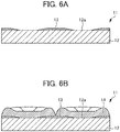
- the nickel 14 begins to be electrodeposited and precipitated from the conductive portion 12a, grows not only in the thickness (longitudinal) direction but also in the planar (lateral) direction, and is in the state of being piled on the upper portion of the non-conductive film 13 as well.
- the non-conductive film (non-conductive portion) to be formed on the cathode plate has a long service life and can be easily maintained even in the case of being lost (deteriorated).
- the nickel 14 begins to be electrodeposited and precipitated from the conductive portion 12a, grows not only in the longitudinal direction but also in the lateral direction, and thus is in the state of gradually being piled on the non-conductive film 13 as well when blobby electric nickel is produced by using the cathode plate 11 as illustrated in Fig. 5 and Fig. 6 .
- the part of the thin non-conductive film 13 to be formed in the vicinity of the boundary with the conductive portion 12a is likely to be lost by the stress at the time of electrodeposition of the nickel 14 and the impact at the time of peeling off of the electric nickel as well as the adhesive property of the part with the metal plate 12 is likely to diminish by penetration of the electrolytic solution.
- an object of the present invention is to provide a metal electrodeposition cathode plate in which a non-conductive film on a metal plate is hardly lost and which can be repeatedly used and a production method therefor.
- the inventors of the present invention have carried out intensive investigations in order to solve the problems described above. As a result, it has been found out that the non-conductive film is hardly lost as protrusions are provided on a metal plate to form a conductive portion and a non-conductive film is provided on the metal surface except the protrusions, whereby the present invention has been completed.
- the present invention it is possible to provide a metal electrodeposition cathode plate in which a non-conductive film is hardly lost and which can be repeatedly used and a production method therefor.
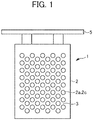
- a cathode plate 1 includes a metal plate 2 on which a plurality of disc-shaped protrusions 2a is disposed and a non-conductive film 3 formed on the surface of the metal plate 2 except the protrusions 2a as illustrated in Fig. 1 .
- the cathode plate 1 is used, for example, by being hung in an electrolytic cell containing an electrolytic solution containing nickel and an anode by a hanging member 5 and nickel having a desired shape is electrodeposited and precipitated on the surface of the cathode plate as to be described later.
- the material for the metal plate 2 is not particularly limited as long as it is a metal which is less susceptible to corrosion by the electrolytic solution to be used and forms only loose bonding with an electrodeposit such as nickel, but preferred examples thereof may include titanium and stainless steel.
- the non-conductive film 3 is formed on the flat area 2b having a concave step formed by the adjacent protrusions 2a and thus the non-conductive film 3 having a predetermined thickness is formed.
- the minimum film thickness Y of the non-conductive film 3 is the same as or greater than the height X of the protrusion 2a and it is preferably the same as the height X.
- the impact to be applied to the end portion of the non-conductive film 3 by the nickel 4 is minor and the non-conductive film 3 is hardly lost even when the nickel 4 is peeled off from the cathode plate 1.
- the non-conductive film 3 is hardly lost and it is thus possible to repeatedly use the non-conductive film 3 in electrodeposition without replacing the non-conductive film 3, to decrease the maintenance cost, and to achieve improvement in the productivity.
- a plurality of pieces of blobby electric nickel can be obtained from one cathode plate 1 by peeling off the nickel 4 from the cathode plate 1 after the electrodeposition of nickel is terminated.
- the non-conductive film 3 is hardly lost and it is thus possible to repeatedly use the non-conductive film 3 without replacing the non-conductive film 3, to decrease the maintenance cost, and to achieve improvement in the productivity.
- a plurality of disc-shaped protrusions 2a is formed on the surface of the metal plate 2.
- the parts of the flat plate-shaped metal plate 2 except the protrusions 2a are scraped, the protrusions 2a having a height X are left, and flat areas 2b are thus formed.
- the processing method is not particularly limited, and the formation of flat areas 2b can be conducted by, for example, wet etching processing, end mill processing, and laser processing.
- the protrusions 2a may be formed only on one surface of the metal plate 2 or on both surfaces of the metal plate 2.
- the non-conductive film 3 is formed on the flat areas 2b to be the surface of the metal plate 2 except the protrusions 2a.
- the method for forming the non-conductive film 3 is not particularly limited, and the formation of the non-conductive film 3 can be conducted by screen printing. In a case in which the material for the non-conductive film 3 is a thermosetting resin or a photocurable resin, heat curing or photocuring may be conducted if necessary.
- a cathode plate was fabricated in the same manner as in Example 1 except that the height X of the protrusion of the metal plate was set to 500 ⁇ m and the non-conductive film was formed on the flat area so as to have a predetermined thickness.
- the difference between the minimum film thickness of the non-conductive film and the height of the protrusion was measured at arbitrary 10 places by using a laser displacement meter, and the results were in a range of from -200 to -150 ⁇ m and the minimum film thickness Y of the non-conductive film 3 was thus 300 ⁇ m.
- the minimum film thickness Y of the non-conductive film 3 is thinner than 500 ⁇ m of the height of the protrusion.
- Nickel electrodeposited at the adjacent protrusions and conductive portions are connected to each other and electric nickel having a desired shape cannot be obtained in some cases when the loss of the non-conductive film expands.
- the use was stopped and the number of repetitions up to this time point was evaluated in a case in which the non-conductive film was lost from the boundary with the protrusion in the direction of the flat area by 1 mm or more.
- the use was stopped and the number of repetitions up to this time point was evaluated in a case in which the non-conductive film was lost and the diameter of the conductive portion increased by 1 mm or more as well.
Landscapes
- Chemical & Material Sciences (AREA)
- Engineering & Computer Science (AREA)
- Chemical Kinetics & Catalysis (AREA)
- Electrochemistry (AREA)
- Materials Engineering (AREA)
- Metallurgy (AREA)
- Organic Chemistry (AREA)
- Crystallography & Structural Chemistry (AREA)
- Electrolytic Production Of Metals (AREA)
Applications Claiming Priority (2)
| Application Number | Priority Date | Filing Date | Title |
|---|---|---|---|
| JP2016143531A JP6724624B2 (ja) | 2016-07-21 | 2016-07-21 | 金属電着用陰極板及びその製造方法 |
| PCT/JP2017/025093 WO2018016362A1 (ja) | 2016-07-21 | 2017-07-10 | 金属電着用陰極板及びその製造方法 |
Publications (2)
| Publication Number | Publication Date |
|---|---|
| EP3489395A1 true EP3489395A1 (de) | 2019-05-29 |
| EP3489395A4 EP3489395A4 (de) | 2020-04-08 |
Family
ID=60992989
Family Applications (1)
| Application Number | Title | Priority Date | Filing Date |
|---|---|---|---|
| EP17830882.1A Withdrawn EP3489395A4 (de) | 2016-07-21 | 2017-07-10 | Metallische elektrotauchkathodenplatte und herstellungsverfahren dafür |
Country Status (6)
| Country | Link |
|---|---|
| US (1) | US20190233960A1 (de) |
| EP (1) | EP3489395A4 (de) |
| JP (1) | JP6724624B2 (de) |
| CN (1) | CN109415832A (de) |
| CA (1) | CA3030941C (de) |
| WO (1) | WO2018016362A1 (de) |
Families Citing this family (4)
| Publication number | Priority date | Publication date | Assignee | Title |
|---|---|---|---|---|
| JP6638589B2 (ja) * | 2016-07-21 | 2020-01-29 | 住友金属鉱山株式会社 | 金属電着用陰極板及びその製造方法 |
| WO2019146474A1 (ja) | 2018-01-29 | 2019-08-01 | コニカミノルタ株式会社 | 立体造形用樹脂組成物、立体造形物、および立体造形物の製造方法 |
| KR102017567B1 (ko) * | 2018-11-27 | 2019-09-03 | 주식회사 웨스코일렉트로드 | 전해 제련용 전극 조립체 |
| JP7188219B2 (ja) * | 2019-03-25 | 2022-12-13 | 住友金属鉱山株式会社 | 金属電着用の陰極板 |
Family Cites Families (7)
| Publication number | Priority date | Publication date | Assignee | Title |
|---|---|---|---|---|
| JPS46919Y1 (de) * | 1966-04-04 | 1971-01-13 | ||
| US4040915A (en) * | 1976-06-15 | 1977-08-09 | The International Nickel Company, Inc. | Method for producing regular electronickel or S nickel rounds from electroplating baths giving highly stressed deposits |
| JPS6038678Y2 (ja) * | 1981-05-15 | 1985-11-19 | 住友金属鉱山株式会社 | 金属電着用母板 |
| JPS6288754U (de) * | 1985-11-25 | 1987-06-06 | ||
| JPH10317197A (ja) * | 1997-05-14 | 1998-12-02 | Sumitomo Metal Mining Co Ltd | メッキ用電気ニッケル、その製造用陰極板及び製造方法 |
| JP2008106292A (ja) * | 2006-10-24 | 2008-05-08 | Sumitomo Metal Mining Co Ltd | 特殊形状電気ニッケルの電解採取用カソードの製造方法 |
| WO2010028428A1 (en) * | 2008-09-09 | 2010-03-18 | Steelmore Holdings Pty Ltd | A cathode and a method of forming a cathode |
-
2016
- 2016-07-21 JP JP2016143531A patent/JP6724624B2/ja active Active
-
2017
- 2017-07-10 CA CA3030941A patent/CA3030941C/en active Active
- 2017-07-10 EP EP17830882.1A patent/EP3489395A4/de not_active Withdrawn
- 2017-07-10 CN CN201780040988.6A patent/CN109415832A/zh active Pending
- 2017-07-10 US US16/317,141 patent/US20190233960A1/en not_active Abandoned
- 2017-07-10 WO PCT/JP2017/025093 patent/WO2018016362A1/ja not_active Ceased
Also Published As
| Publication number | Publication date |
|---|---|
| CA3030941A1 (en) | 2018-01-25 |
| JP6724624B2 (ja) | 2020-07-15 |
| JP2018012865A (ja) | 2018-01-25 |
| EP3489395A4 (de) | 2020-04-08 |
| US20190233960A1 (en) | 2019-08-01 |
| CN109415832A (zh) | 2019-03-01 |
| WO2018016362A1 (ja) | 2018-01-25 |
| CA3030941C (en) | 2020-12-15 |
Similar Documents
| Publication | Publication Date | Title |
|---|---|---|
| EP3633074B1 (de) | Kathodenplatte für metallgalvanotechnik und herstellungsverfahren dafür | |
| EP3489395A1 (de) | Metallische elektrotauchkathodenplatte und herstellungsverfahren dafür | |
| CN103068155A (zh) | 柔性印刷基板及其制造方法 | |
| US11339465B2 (en) | Vapor deposition mask substrate, vapor deposition mask substrate manufacturing method, vapor deposition mask manufacturing method, and display device manufacturing method | |
| SE448001B (sv) | Katodiskt utfelld metallprodukt | |
| US20200095697A1 (en) | Manufacturing Apparatus of Electrolytic Copper Foil | |
| KR101879080B1 (ko) | 철-니켈 합금 포일 제조장치 | |
| JP6638589B2 (ja) | 金属電着用陰極板及びその製造方法 | |
| KR101282327B1 (ko) | 미세 금속 패턴을 가지는 필름 제조 방법 | |
| JP6737035B2 (ja) | 金属電着用陰極板及びその製造方法 | |
| JP6737036B2 (ja) | 金属電着用陰極板及びその製造方法 | |
| US2225733A (en) | Process for the electrolytic production of metal screens | |
| JP7188218B2 (ja) | 金属電着用の陰極板 | |
| JP7188219B2 (ja) | 金属電着用の陰極板 | |
| JP7238524B2 (ja) | 金属電着用の陰極板 | |
| JP7188217B2 (ja) | 金属電着用の陰極板の製造方法 | |
| JP7188216B2 (ja) | 金属電着用の陰極板の製造方法 | |
| JP2019108592A (ja) | ボタン型電気ニッケルの製造用母板、その製造方法、及びそれを用いたボタン型電気ニッケルの製造方法 | |
| JP3416620B2 (ja) | 電解銅箔製造装置及び電解銅箔製造方法 | |
| JP6825470B2 (ja) | 試験電着用陰極板、及びその製造方法 | |
| JP6760191B2 (ja) | 特殊形状電着物の製造方法 | |
| JP2024008385A (ja) | 金属電着用の陰極板の製造方法 | |
| WO2006112696A2 (en) | Method for electroforming a studded plate and a copy die, electroforming die for this method, and copy die |
Legal Events
| Date | Code | Title | Description |
|---|---|---|---|
| STAA | Information on the status of an ep patent application or granted ep patent |
Free format text: STATUS: THE INTERNATIONAL PUBLICATION HAS BEEN MADE |
|
| PUAI | Public reference made under article 153(3) epc to a published international application that has entered the european phase |
Free format text: ORIGINAL CODE: 0009012 |
|
| STAA | Information on the status of an ep patent application or granted ep patent |
Free format text: STATUS: REQUEST FOR EXAMINATION WAS MADE |
|
| 17P | Request for examination filed |
Effective date: 20190204 |
|
| AK | Designated contracting states |
Kind code of ref document: A1 Designated state(s): AL AT BE BG CH CY CZ DE DK EE ES FI FR GB GR HR HU IE IS IT LI LT LU LV MC MK MT NL NO PL PT RO RS SE SI SK SM TR |
|
| AX | Request for extension of the european patent |
Extension state: BA ME |
|
| DAV | Request for validation of the european patent (deleted) | ||
| DAX | Request for extension of the european patent (deleted) | ||
| A4 | Supplementary search report drawn up and despatched |
Effective date: 20200309 |
|
| RIC1 | Information provided on ipc code assigned before grant |
Ipc: C25C 7/08 20060101ALI20200303BHEP Ipc: C25C 7/02 20060101AFI20200303BHEP Ipc: C25C 1/08 20060101ALI20200303BHEP Ipc: C25D 17/12 20060101ALI20200303BHEP |
|
| STAA | Information on the status of an ep patent application or granted ep patent |
Free format text: STATUS: EXAMINATION IS IN PROGRESS |
|
| 17Q | First examination report despatched |
Effective date: 20220210 |
|
| RIC1 | Information provided on ipc code assigned before grant |
Ipc: C25D 17/16 19740701ALI20221231BHEP Ipc: C25D 1/20 19740701ALI20221231BHEP Ipc: C25D 1/00 19740701ALI20221231BHEP Ipc: C25D 17/12 19740701ALI20221231BHEP Ipc: C25C 1/08 19740701ALI20221231BHEP Ipc: C25C 7/08 19740701ALI20221231BHEP Ipc: C25C 7/02 19740701AFI20221231BHEP |
|
| GRAP | Despatch of communication of intention to grant a patent |
Free format text: ORIGINAL CODE: EPIDOSNIGR1 |
|
| STAA | Information on the status of an ep patent application or granted ep patent |
Free format text: STATUS: GRANT OF PATENT IS INTENDED |
|
| INTG | Intention to grant announced |
Effective date: 20230310 |
|
| STAA | Information on the status of an ep patent application or granted ep patent |
Free format text: STATUS: THE APPLICATION IS DEEMED TO BE WITHDRAWN |
|
| 18D | Application deemed to be withdrawn |
Effective date: 20230721 |