EP3489384A1 - Fine metal mask, display substrate, and alignment method therefor - Google Patents
Fine metal mask, display substrate, and alignment method therefor Download PDFInfo
- Publication number
- EP3489384A1 EP3489384A1 EP17852374.2A EP17852374A EP3489384A1 EP 3489384 A1 EP3489384 A1 EP 3489384A1 EP 17852374 A EP17852374 A EP 17852374A EP 3489384 A1 EP3489384 A1 EP 3489384A1
- Authority
- EP
- European Patent Office
- Prior art keywords
- alignment
- fine metal
- metal mask
- holes
- pattern region
- Prior art date
- Legal status (The legal status is an assumption and is not a legal conclusion. Google has not performed a legal analysis and makes no representation as to the accuracy of the status listed.)
- Granted
Links
Images





Classifications
-
- C—CHEMISTRY; METALLURGY
- C23—COATING METALLIC MATERIAL; COATING MATERIAL WITH METALLIC MATERIAL; CHEMICAL SURFACE TREATMENT; DIFFUSION TREATMENT OF METALLIC MATERIAL; COATING BY VACUUM EVAPORATION, BY SPUTTERING, BY ION IMPLANTATION OR BY CHEMICAL VAPOUR DEPOSITION, IN GENERAL; INHIBITING CORROSION OF METALLIC MATERIAL OR INCRUSTATION IN GENERAL
- C23C—COATING METALLIC MATERIAL; COATING MATERIAL WITH METALLIC MATERIAL; SURFACE TREATMENT OF METALLIC MATERIAL BY DIFFUSION INTO THE SURFACE, BY CHEMICAL CONVERSION OR SUBSTITUTION; COATING BY VACUUM EVAPORATION, BY SPUTTERING, BY ION IMPLANTATION OR BY CHEMICAL VAPOUR DEPOSITION, IN GENERAL
- C23C14/00—Coating by vacuum evaporation, by sputtering or by ion implantation of the coating forming material
- C23C14/04—Coating on selected surface areas, e.g. using masks
- C23C14/042—Coating on selected surface areas, e.g. using masks using masks
-
- H—ELECTRICITY
- H10—SEMICONDUCTOR DEVICES; ELECTRIC SOLID-STATE DEVICES NOT OTHERWISE PROVIDED FOR
- H10W—GENERIC PACKAGES, INTERCONNECTIONS, CONNECTORS OR OTHER CONSTRUCTIONAL DETAILS OF DEVICES COVERED BY CLASS H10
- H10W46/00—Marks applied to devices, e.g. for alignment or identification
-
- C—CHEMISTRY; METALLURGY
- C23—COATING METALLIC MATERIAL; COATING MATERIAL WITH METALLIC MATERIAL; CHEMICAL SURFACE TREATMENT; DIFFUSION TREATMENT OF METALLIC MATERIAL; COATING BY VACUUM EVAPORATION, BY SPUTTERING, BY ION IMPLANTATION OR BY CHEMICAL VAPOUR DEPOSITION, IN GENERAL; INHIBITING CORROSION OF METALLIC MATERIAL OR INCRUSTATION IN GENERAL
- C23C—COATING METALLIC MATERIAL; COATING MATERIAL WITH METALLIC MATERIAL; SURFACE TREATMENT OF METALLIC MATERIAL BY DIFFUSION INTO THE SURFACE, BY CHEMICAL CONVERSION OR SUBSTITUTION; COATING BY VACUUM EVAPORATION, BY SPUTTERING, BY ION IMPLANTATION OR BY CHEMICAL VAPOUR DEPOSITION, IN GENERAL
- C23C14/00—Coating by vacuum evaporation, by sputtering or by ion implantation of the coating forming material
- C23C14/06—Coating by vacuum evaporation, by sputtering or by ion implantation of the coating forming material characterised by the coating material
- C23C14/12—Organic material
-
- C—CHEMISTRY; METALLURGY
- C23—COATING METALLIC MATERIAL; COATING MATERIAL WITH METALLIC MATERIAL; CHEMICAL SURFACE TREATMENT; DIFFUSION TREATMENT OF METALLIC MATERIAL; COATING BY VACUUM EVAPORATION, BY SPUTTERING, BY ION IMPLANTATION OR BY CHEMICAL VAPOUR DEPOSITION, IN GENERAL; INHIBITING CORROSION OF METALLIC MATERIAL OR INCRUSTATION IN GENERAL
- C23C—COATING METALLIC MATERIAL; COATING MATERIAL WITH METALLIC MATERIAL; SURFACE TREATMENT OF METALLIC MATERIAL BY DIFFUSION INTO THE SURFACE, BY CHEMICAL CONVERSION OR SUBSTITUTION; COATING BY VACUUM EVAPORATION, BY SPUTTERING, BY ION IMPLANTATION OR BY CHEMICAL VAPOUR DEPOSITION, IN GENERAL
- C23C14/00—Coating by vacuum evaporation, by sputtering or by ion implantation of the coating forming material
- C23C14/22—Coating by vacuum evaporation, by sputtering or by ion implantation of the coating forming material characterised by the process of coating
- C23C14/24—Vacuum evaporation
-
- C—CHEMISTRY; METALLURGY
- C23—COATING METALLIC MATERIAL; COATING MATERIAL WITH METALLIC MATERIAL; CHEMICAL SURFACE TREATMENT; DIFFUSION TREATMENT OF METALLIC MATERIAL; COATING BY VACUUM EVAPORATION, BY SPUTTERING, BY ION IMPLANTATION OR BY CHEMICAL VAPOUR DEPOSITION, IN GENERAL; INHIBITING CORROSION OF METALLIC MATERIAL OR INCRUSTATION IN GENERAL
- C23C—COATING METALLIC MATERIAL; COATING MATERIAL WITH METALLIC MATERIAL; SURFACE TREATMENT OF METALLIC MATERIAL BY DIFFUSION INTO THE SURFACE, BY CHEMICAL CONVERSION OR SUBSTITUTION; COATING BY VACUUM EVAPORATION, BY SPUTTERING, BY ION IMPLANTATION OR BY CHEMICAL VAPOUR DEPOSITION, IN GENERAL
- C23C14/00—Coating by vacuum evaporation, by sputtering or by ion implantation of the coating forming material
- C23C14/22—Coating by vacuum evaporation, by sputtering or by ion implantation of the coating forming material characterised by the process of coating
- C23C14/54—Controlling or regulating the coating process
-
- H—ELECTRICITY
- H10—SEMICONDUCTOR DEVICES; ELECTRIC SOLID-STATE DEVICES NOT OTHERWISE PROVIDED FOR
- H10K—ORGANIC ELECTRIC SOLID-STATE DEVICES
- H10K71/00—Manufacture or treatment specially adapted for the organic devices covered by this subclass
- H10K71/10—Deposition of organic active material
- H10K71/16—Deposition of organic active material using physical vapour deposition [PVD], e.g. vacuum deposition or sputtering
- H10K71/166—Deposition of organic active material using physical vapour deposition [PVD], e.g. vacuum deposition or sputtering using selective deposition, e.g. using a mask
-
- H—ELECTRICITY
- H10—SEMICONDUCTOR DEVICES; ELECTRIC SOLID-STATE DEVICES NOT OTHERWISE PROVIDED FOR
- H10K—ORGANIC ELECTRIC SOLID-STATE DEVICES
- H10K77/00—Constructional details of devices covered by this subclass and not covered by groups H10K10/80, H10K30/80, H10K50/80 or H10K59/80
- H10K77/10—Substrates, e.g. flexible substrates
-
- H—ELECTRICITY
- H10—SEMICONDUCTOR DEVICES; ELECTRIC SOLID-STATE DEVICES NOT OTHERWISE PROVIDED FOR
- H10K—ORGANIC ELECTRIC SOLID-STATE DEVICES
- H10K59/00—Integrated devices, or assemblies of multiple devices, comprising at least one organic light-emitting element covered by group H10K50/00
- H10K59/30—Devices specially adapted for multicolour light emission
- H10K59/35—Devices specially adapted for multicolour light emission comprising red-green-blue [RGB] subpixels
- H10K59/352—Devices specially adapted for multicolour light emission comprising red-green-blue [RGB] subpixels the areas of the RGB subpixels being different
-
- H—ELECTRICITY
- H10—SEMICONDUCTOR DEVICES; ELECTRIC SOLID-STATE DEVICES NOT OTHERWISE PROVIDED FOR
- H10K—ORGANIC ELECTRIC SOLID-STATE DEVICES
- H10K59/00—Integrated devices, or assemblies of multiple devices, comprising at least one organic light-emitting element covered by group H10K50/00
- H10K59/30—Devices specially adapted for multicolour light emission
- H10K59/35—Devices specially adapted for multicolour light emission comprising red-green-blue [RGB] subpixels
- H10K59/353—Devices specially adapted for multicolour light emission comprising red-green-blue [RGB] subpixels characterised by the geometrical arrangement of the RGB subpixels
-
- H—ELECTRICITY
- H10—SEMICONDUCTOR DEVICES; ELECTRIC SOLID-STATE DEVICES NOT OTHERWISE PROVIDED FOR
- H10P—GENERIC PROCESSES OR APPARATUS FOR THE MANUFACTURE OR TREATMENT OF DEVICES COVERED BY CLASS H10
- H10P72/00—Handling or holding of wafers, substrates or devices during manufacture or treatment thereof
- H10P72/50—Handling or holding of wafers, substrates or devices during manufacture or treatment thereof for positioning, orientation or alignment
-
- H—ELECTRICITY
- H10—SEMICONDUCTOR DEVICES; ELECTRIC SOLID-STATE DEVICES NOT OTHERWISE PROVIDED FOR
- H10W—GENERIC PACKAGES, INTERCONNECTIONS, CONNECTORS OR OTHER CONSTRUCTIONAL DETAILS OF DEVICES COVERED BY CLASS H10
- H10W46/00—Marks applied to devices, e.g. for alignment or identification
- H10W46/301—Marks applied to devices, e.g. for alignment or identification for alignment
-
- Y—GENERAL TAGGING OF NEW TECHNOLOGICAL DEVELOPMENTS; GENERAL TAGGING OF CROSS-SECTIONAL TECHNOLOGIES SPANNING OVER SEVERAL SECTIONS OF THE IPC; TECHNICAL SUBJECTS COVERED BY FORMER USPC CROSS-REFERENCE ART COLLECTIONS [XRACs] AND DIGESTS
- Y02—TECHNOLOGIES OR APPLICATIONS FOR MITIGATION OR ADAPTATION AGAINST CLIMATE CHANGE
- Y02E—REDUCTION OF GREENHOUSE GAS [GHG] EMISSIONS, RELATED TO ENERGY GENERATION, TRANSMISSION OR DISTRIBUTION
- Y02E10/00—Energy generation through renewable energy sources
- Y02E10/50—Photovoltaic [PV] energy
- Y02E10/549—Organic PV cells
Definitions
- the present disclosure relates to the field of evaporation technology, particularly to a fine metal mask, a display substrate and an alignment method thereof.
- the organic material layer with required patterns is formed on the OLED substrate masked by a mask plate with patterns by vacuum evaporation.
- the pattern region of the mask plate has a plurality of openings through which organic materials are plated onto the pixel region of the OLED substrate during evaporation, thereby pixels made of organic materials are formed in the pixel region.
- mask plates with different patterns need to be used.
- the mask plate includes a mask and a mesh frame, and the mask need to be tensioned on the mesh frame by a tension device when it is combined with the mesh frame (referred to as tension operation), so the mask is fixed on the mesh frame to form a required mask plate.
- the present application provides a fine metal mask for evaporation, a display substrate and an alignment method thereof, which improve alignment accuracy.
- a fine metal mask comprising a pattern region including a plurality of openings and a plurality of alignment holes located outside the pattern region.
- the alignment holes are located outside the pattern region, the alignment holes are easily identified when the fine metal mask is tensioned, so it is tensioned on the mesh frame using a tension device, and the alignment holes also contribute to the accurate alignment between the fine metal mask and the OLED substrate, thereby the yield of the product obtained by evaporation is improved.
- the pattern region has a circular shape, and the plurality of alignment holes are evenly distributed along the circumferential direction of the pattern region.
- the plurality of alignment holes serve as a tension position reference when the fine metal mask is tensioned on the mesh frame, and since the plurality of alignment holes are evenly distributed along the circumferential direction of the pattern region, so that the fine metal mask can be positioned more accurately and stabilized on the mesh frame easily.
- the number of the plurality of alignment holes is at least three.
- the plurality of alignment holes have shapes and sizes same to that of the plurality of openings in the pattern region, respectively.
- the alignment holes and the openings in the pattern region of the fine metal mask have the same shapes and sizes, the alignment holes and the openings in the pattern region of the fine metal mask can be opened by using the same opening mold when making the fine metal mask, which is convenient to operate.
- the plurality of alignment holes have arrangement same to that of the plurality of openings in the pattern region.
- the alignment holes can be opened according to the opening manner of the openings in the pattern region when making the fine metal mask.
- a display substrate adapted to cooperate with the above fine metal mask during evaporation.
- the display substrate comprises a pixel region corresponding to the pattern region in the fine metal mask and a plurality of alignment marks located outside the pixel region, and the position of each alignment mark in the display substrate corresponds to the position of the corresponding one of the plurality of alignment holes in the fine metal mask;
- the alignment marks are alignment fitting holes.
- the opening size of the alignment fitting holes is smaller than that of the alignment holes, so that the alignment fitting holes are visible through the openings of the alignment holes when the fine metal mask is placed on the display substrate and the alignment fitting holes are aligned with the alignment holes.
- the alignment fitting holes Since the opening size of the alignment fitting holes is smaller than that of the alignment holes, the alignment fitting holes are visible through the openings of the alignment holes when the alignment fitting holes are aligned with the alignment holes, thus when the fine metal mask is aligned with the display substrate and the PPA debugging of the fine metal mask is performed, the alignment fitting holes in the display substrate can be easily identified through the openings of the alignment holes in the fine metal mask, thereby the relative position between the fine metal mask and the display substrate is adjusted to complete the alignment.
- an alignment method of a fine metal mask for evaporation comprising the following steps:
- the used fine metal mask has a plurality of alignment holes outside the pattern region which are independent of the pattern region and thus can be easily identified, thereby the alignment accuracy between the fine metal mask and the display substrate is ensured and the yield of the product is improved.
- the method comprises providing a plurality of fine metal masks, wherein the pattern region in each fine metal mask has different pixel patterns, and each fine metal mask is used to form pixels of single color on the display substrate during the evaporation.
- the alignment marks on the display substrate are alignment fitting holes.
- the size of the alignment marks is smaller than the opening size of the alignment holes, so that the alignment marks are visible through the openings of the alignment holes when the alignment marks are aligned with the alignment holes.
- adjusting the position of the fine metal mask to align the plurality of alignment holes in the fine metal mask with the corresponding one of the plurality of alignment marks in the display substrate respectively comprises: adjusting the position of the fine metal mask to locate each of the plurality of alignment marks in the display substrate at the central position of the opening of the corresponding one of the plurality of alignment holes in the fine metal mask.
- a fine metal mask having alignment holes provided outside the pattern region and a display substrate having alignment marks provided outside the pixel region are used, and the fine metal mask can be tensioned at a correct position on the mesh frame by identifying the alignment holes of the fine metal mask, and the accurate positioning of the fine metal mask and the display substrate can be realized by aligning the positions of the alignment holes of the fine metal mask and the alignment marks of the display substrate, thereby the yield of the product obtained by evaporation is improved.
- the evaporation of the OLED substrate is described below as an example, and it can be understood by those skilled in the art that the fine metal mask and the alignment method of the present disclosure can be applied to other suitable types of display substrates.
- the present disclosure provides an alignment method of a fine metal mask for evaporation comprising the following steps:
- the method further comprises providing a plurality of fine metal masks, wherein the pattern region in each fine metal mask has different pixel pattern, and each fine metal mask is used to form pixels of single color on the OLED substrate during evaporation.
- the above method needs to provide three fine metal masks which are separately used to form red, green and blue pixels on the OLED substrate during evaporation.
- the fine metal mask of the present disclosure will be described in detail.
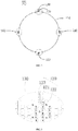
- FIG. 2 shows a fine metal mask 100 according to one embodiment of the present disclosure.
- the fine metal mask 100 comprises a pattern region 110 and a plurality of alignment holes 120 located outside the pattern region 110.
- the pattern region 110 of the fine metal mask 100 has a circular shape, and the alignment holes 120 are evenly distributed along the circumferential direction of the pattern region 110.
- there are four circumferentially evenly distributed positions on the outer circumference of the pattern region 110 i.e., a first position 130, a second position 140, a third position 150 and a fourth position 160. The four positions are provided with alignment holes 120, respectively.
- FIG. 2 shows a fine metal mask 100 according to one embodiment of the present disclosure.
- the fine metal mask 100 comprises a pattern region 110 and a plurality of alignment holes 120 located outside the pattern region 110.
- the pattern region 110 of the fine metal mask 100 has a circular shape, and the alignment holes 120 are evenly distributed along the circumferential direction of the pattern region 110.
- the alignment holes 120 comprise three types of alignment holes, such as R alignment hole 121 for evaporating R pixels, G alignment hole 122 for evaporating G pixels, and B alignment hole 123 for evaporating B pixels.
- R alignment hole 121 for evaporating R pixels the pattern regions for evaporating the three RGB color pixels are simultaneously shown in FIGS. 3-6 , and the R alignment hole 121, the G alignment hole 122 and the B alignment hole 123 also appear simultaneously.
- the R alignment hole 121 exists only in the fine metal mask for evaporating the R pixel
- the G alignment hole 122 exists only in the fine metal mask for evaporating the G pixel
- the B alignment hole 123 exists only in the fine metal mask for evaporating the B pixel. All schematic drawings of the present disclosure are therefore only for illustrative purposes and do not represent actual cases.
- the pattern region 110 is used to form a pixel region on the OLED substrate during evaporation, and the pixel region will finally be formed as an effective display region on the display screen.
- Organic materials are deposited on the pixel region of the OLED substrate through these openings during evaporation, thereby pixels composed of the organic materials are formed in the pixel region.
- the pattern region 110 has a circular shape.
- the shape of the pattern region 110 is not limited thereto, and it can be understood by those skilled in the art that the pattern region may be any suitable shape as desired, such as a triangle, a rectangle, a square, or other polygons, or an ellipse, an ellipse-like shape, or the like.
- the plurality of alignment holes 120 of the fine metal mask 100 are evenly distributed along the circumferential direction of the pattern region 110.
- the plurality of alignment holes serve as a tension position reference when the fine metal mask is tensioned on the mesh frame, and since these alignment holes 120 are evenly distributed along the circumferential direction of the pattern region 110 to form positioning reference points spaced apart from each other, the fine metal mask can be positioned on the mesh frame more accurately and stabilized on the mesh frame easily.
- the number of the alignment holes is four. In other embodiments, the number of the alignment holes may be set to three, five, or more than five as desired.
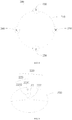
- FIG. 7 shows a schematic top view of the fine metal mask according to another embodiment of the present disclosure.
- three alignment holes 120 are provided outside the pattern region 110 of the fine metal mask 100 (as described above, for convenience of explanation, the R alignment hole, the G alignment hole and the B alignment hole are simultaneously shown in this embodiment).
- alignment holes 120 are respectively provided at three positions 170, 180 and 190 evenly distributed along the circumferential direction of the circular pattern region 110.
- the plurality of alignment holes 120 of the fine metal mask 100 are adjacent to the pattern region 110.
- the alignment holes are disposed adjacent to the pattern region, and the area of the identification region may be reduced when the alignment hole is identified. It can be understood by those skilled in the art that the alignment holes may be spaced apart from the pattern region, so that it is easy to effectively distinguish the alignment holes from the pattern region when the alignment holes are identified, but spacing distance should not be too large, or it would result in an excessively large identification region.
- the R alignment hole 121 and the G alignment hole 122 present a square whose apex angles are rounded corners, and the B alignment hole 123 presents a closed pattern with arc, preferably semi-circular shapes at two ends and a rectangle in the middle.
- the R alignment hole 121, the G alignment hole 122 and the B alignment hole 123 have the same shape and size as that of the openings of the corresponding color pixels in the pattern region, thus, the alignment holes and the openings in the pattern region of the fine metal mask can be opened by using the same opening mold when making the fine metal mask, which is convenient to operate.
- the alignment holes and the openings in the pattern region of the fine metal mask have the same arrangement, so that the alignment holes can be opened according to the opening manner of the openings in the pattern region when making the fine metal mask. It can be understood by those skilled in the art that the shape and size of the alignment holes may be different from that of the openings in the pattern region, so that it is easy to effectively distinguish the alignment holes from the pattern region when the alignment holes are identified.
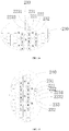
- FIG. 8 shows an OLED substrate 200 according to one embodiment of the present disclosure.
- the OLED substrate 200 has a pixel region 210 corresponding to the pattern region 110 on the fine metal mask 100 and four alignment marks disposed corresponding to the alignment holes 120 in the fine metal mask 100.
- the pixel region 210 will form an effective display region of the display.
- the alignment marks in the embodiment are alignment fitting holes 220.
- the four alignment fitting holes 220 are respectively located at a first position 230, a second position 240, a third position 250 and a fourth position 260 evenly distributed along the circumferential direction of the pixel region 210 on the OLED substrate 200.
- the alignment marks may also be other types of marks that can function as a precise alignment.
- the R alignment fitting hole 221, the G alignment fitting hole 222, the first B alignment fitting hole 2231 and the second B alignment fitting hole 2232 all have a rectangular shape similar to the opening shape of the alignment holes.
- the shape of the alignment fitting hole 220 in the OLED substrate 200 of the present disclosure is not limited thereto, and may also be significantly different from the shape of the alignment hole 120 in the fine metal mask 100, or any other shape.
- the opening size of the alignment fitting holes 220 is smaller than the opening size of the alignment holes 120 in the fine metal mask 100, so that the alignment fitting holes 220 are visible through the openings of the alignment holes 120 when the alignment fitting holes 220 are aligned with the alignment holes 120.
- the alignment fitting holes in the OLED substrate can be easily identified through the openings of the alignment holes in the fine metal mask, thereby the relative position between the fine metal mask and the OLED substrate is adjusted to complete the alignment.
- the position of the fine metal mask needs to be adjusted after the fine metal mask is placed on the OLED substrate, so that all the alignment fitting holes in the OLED substrate are located in the central positions of the openings of the alignment holes in the fine metal mask.
- the number of the alignment fitting holes 220 and that of the alignment holes 120 is the same, and the positions are in one-to-one correspondence, thereby the alignment accuracy between the OLED substrate 200 and the fine metal mask 100 is improved.
- the alignment fitting hole 220 includes an R alignment fitting hole 221, a G alignment fitting hole 222 and a B alignment fitting hole 223 corresponding to the R alignment hole 121, the G alignment hole 122 and the B alignment hole 123, respectively.
- the B alignment mark is designed to have a first B alignment fitting hole 2231 and a second B alignment fitting hole 2232 arranged along the length direction of the B alignment mark.
- the degree of position alignment between the B alignment hole and the B alignment mark can be determined more accurately by adjusting the position relationship between the upper half part of the B alignment hole 123 and the first B alignment fitting hole 2231 and the position relationship between the lower half part of the B alignment hole 123 and the second B alignment fitting hole 2232, respectively.
- FIG. 13 shows a schematic bottom view of the OLED substrate 200 obtained by evaporation after the fine metal mask and the OLED substrate are aligned and combined.
- FIGS. 14-17 are schematic enlarged views of four positions of the OLED substrate 200, namely, a first position 230, a second position 240, a third position 250, and a fourth position 260, respectively.
- the evaporated OLED substrate 200 includes a pixel region 310 coated with an organic material layer and an alignment region located outside the pixel region 310.
- the alignment region includes an R alignment region 231, a G alignment region 232 and a B alignment region 233.
- the first position 230 will be described as an example.
- the opening size of the alignment fitting holes of the OLED substrate is smaller than that of the alignment holes of the fine metal mask, and the alignment fitting holes of the OLED substrate are located at the central positions of the alignment holes of the fine metal mask during alignment, the thickness of the organic materials at the positions where the alignment fitting hole are located in the opening region of the alignment hole is thicker than that at other positions in the opening region of the alignment hole after evaporation. In this way, the relative position between the alignment holes and the alignment fitting holes during the evaporation can be easily determined in the alignment region of the evaporated OLED substrate.
- the position of the R alignment fitting hole 221 can be identified in the R alignment region 231 formed by the opening of the R alignment hole
- the position of the G alignment fitting hole 222 can be identified in the G alignment region 232 formed by the opening of the G alignment hole
- the positions of the first B alignment fitting hole 2231 and the second B alignment fitting hole 2232 can be identified in the B alignment region 233 formed by the opening of the B alignment hole.
- the position relationship of the alignment fitting hole with respect to the opening of the alignment hole can be used as the reference of PPA debugging.
- the R alignment fitting hole 221 deviates from the center of the R alignment region 231, it is necessary to adjust the position of the fine metal mask with respect to the OLED substrate during the next evaporation, so that the R alignment fitting hole 221 is located at the central position of the opening of the R alignment hole, i.e., the R alignment fitting hole 221 is axially aligned with the R alignment hole.
Landscapes
- Chemical & Material Sciences (AREA)
- Engineering & Computer Science (AREA)
- Chemical Kinetics & Catalysis (AREA)
- Materials Engineering (AREA)
- Mechanical Engineering (AREA)
- Metallurgy (AREA)
- Organic Chemistry (AREA)
- Manufacturing & Machinery (AREA)
- Electroluminescent Light Sources (AREA)
- Physical Vapour Deposition (AREA)
Abstract
Description
- The present disclosure relates to the field of evaporation technology, particularly to a fine metal mask, a display substrate and an alignment method thereof.
- Currently, in the process of making an organic material layer of display panel such as OLED (Organic Light-Emitting Diode) display screen, the organic material layer with required patterns is formed on the OLED substrate masked by a mask plate with patterns by vacuum evaporation. The pattern region of the mask plate has a plurality of openings through which organic materials are plated onto the pixel region of the OLED substrate during evaporation, thereby pixels made of organic materials are formed in the pixel region. In order to form pixels of different colors on the OLED substrate, mask plates with different patterns need to be used. For example, in order to form pixels of three colors of red, green and blue on the OLED substrate, it is necessary to form red pixels on the OLED substrate using a mask plate having red pixel patterns, to form green pixels on the OLED substrate using a mask plate having green pixel patterns, and to form blue pixels on the OLED substrate using a mask plate having blue pixel patterns. The mask plate includes a mask and a mesh frame, and the mask need to be tensioned on the mesh frame by a tension device when it is combined with the mesh frame (referred to as tension operation), so the mask is fixed on the mesh frame to form a required mask plate.
- During the evaporation process of the organic material layer, it is necessary to debug the PPA (Pixel Position Accuracy) of the fine metal mask and realize accurate alignment between the fine metal mask and the substrate during this process, thereby normal debugging of the PPA is ensured. In the actual operation, it is difficult to realize precise alignment.
- Based on this, the present application provides a fine metal mask for evaporation, a display substrate and an alignment method thereof, which improve alignment accuracy.
- According to an aspect of the present disclosure, there is provided a fine metal mask comprising a pattern region including a plurality of openings and a plurality of alignment holes located outside the pattern region.
- In the fine metal mask according to the aspect, since the alignment holes are located outside the pattern region, the alignment holes are easily identified when the fine metal mask is tensioned, so it is tensioned on the mesh frame using a tension device, and the alignment holes also contribute to the accurate alignment between the fine metal mask and the OLED substrate, thereby the yield of the product obtained by evaporation is improved.
- In one embodiment, the pattern region has a circular shape, and the plurality of alignment holes are evenly distributed along the circumferential direction of the pattern region.
- The plurality of alignment holes serve as a tension position reference when the fine metal mask is tensioned on the mesh frame, and since the plurality of alignment holes are evenly distributed along the circumferential direction of the pattern region, so that the fine metal mask can be positioned more accurately and stabilized on the mesh frame easily.
- In one embodiment, the number of the plurality of alignment holes is at least three.
- In one embodiment, the plurality of alignment holes have shapes and sizes same to that of the plurality of openings in the pattern region, respectively.
- Since the alignment holes and the openings in the pattern region of the fine metal mask have the same shapes and sizes, the alignment holes and the openings in the pattern region of the fine metal mask can be opened by using the same opening mold when making the fine metal mask, which is convenient to operate.
- In one embodiment, the plurality of alignment holes have arrangement same to that of the plurality of openings in the pattern region.
- Since the plurality of alignment holes and the plurality of openings in the pattern region of the above fine metal mask have the same arrangement, the alignment holes can be opened according to the opening manner of the openings in the pattern region when making the fine metal mask.
- According to another aspect of the present disclosure, there is provided a display substrate adapted to cooperate with the above fine metal mask during evaporation. The display substrate comprises a pixel region corresponding to the pattern region in the fine metal mask and a plurality of alignment marks located outside the pixel region, and the position of each alignment mark in the display substrate corresponds to the position of the corresponding one of the plurality of alignment holes in the fine metal mask;
- In one embodiment, the alignment marks are alignment fitting holes.
- In one embodiment, the opening size of the alignment fitting holes is smaller than that of the alignment holes, so that the alignment fitting holes are visible through the openings of the alignment holes when the fine metal mask is placed on the display substrate and the alignment fitting holes are aligned with the alignment holes.
- Since the opening size of the alignment fitting holes is smaller than that of the alignment holes, the alignment fitting holes are visible through the openings of the alignment holes when the alignment fitting holes are aligned with the alignment holes, thus when the fine metal mask is aligned with the display substrate and the PPA debugging of the fine metal mask is performed, the alignment fitting holes in the display substrate can be easily identified through the openings of the alignment holes in the fine metal mask, thereby the relative position between the fine metal mask and the display substrate is adjusted to complete the alignment.
- According to still another aspect of the present disclosure, there is provided an alignment method of a fine metal mask for evaporation comprising the following steps:
- providing a fine metal mask including a pattern region having a plurality of openings and a plurality of alignment holes defined outside the pattern region;
- identifying the plurality of alignment holes in the fine metal mask, and tensioning the fine metal mask on the mesh frame via a tension device according to the identified alignment holes, and a mask plate being formed by the fine metal mask and the mesh frame;
- providing a display substrate which includes a pixel region and a plurality of alignment marks, wherein the pixel region corresponds to the pattern region in the fine metal mask, and the position of each of the plurality of alignment marks in the display substrate corresponds to the position of the corresponding one of the plurality of alignment holes in the fine metal mask;
- placing the mask plate on the display substrate, and adjusting the position of the fine metal mask to align the plurality of alignment holes in the fine metal mask with the corresponding one of the plurality of alignment marks in the display substrate, respectively; and
- performing an evaporation for the assembly of the mask plate and the display substrate by an evaporation source.
- In the above alignment method of the fine metal mask for evaporation, the used fine metal mask has a plurality of alignment holes outside the pattern region which are independent of the pattern region and thus can be easily identified, thereby the alignment accuracy between the fine metal mask and the display substrate is ensured and the yield of the product is improved.
- In one embodiment, the method comprises providing a plurality of fine metal masks, wherein the pattern region in each fine metal mask has different pixel patterns, and each fine metal mask is used to form pixels of single color on the display substrate during the evaporation.
- In one embodiment, the alignment marks on the display substrate are alignment fitting holes.
- In one embodiment, the size of the alignment marks is smaller than the opening size of the alignment holes, so that the alignment marks are visible through the openings of the alignment holes when the alignment marks are aligned with the alignment holes.
- In one embodiment, adjusting the position of the fine metal mask to align the plurality of alignment holes in the fine metal mask with the corresponding one of the plurality of alignment marks in the display substrate respectively comprises: adjusting the position of the fine metal mask to locate each of the plurality of alignment marks in the display substrate at the central position of the opening of the corresponding one of the plurality of alignment holes in the fine metal mask.
- In the alignment method of the fine metal mask for evaporation, a fine metal mask having alignment holes provided outside the pattern region and a display substrate having alignment marks provided outside the pixel region are used, and the fine metal mask can be tensioned at a correct position on the mesh frame by identifying the alignment holes of the fine metal mask, and the accurate positioning of the fine metal mask and the display substrate can be realized by aligning the positions of the alignment holes of the fine metal mask and the alignment marks of the display substrate, thereby the yield of the product obtained by evaporation is improved.
-
-
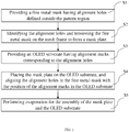
FIG. 1 is a flowchart of the alignment method of the fine metal mask for OLED evaporation according to one embodiment of the present disclosure; -
FIG. 2 is a schematic top view of the fine metal mask according to one embodiment of the present disclosure; -
FIG. 3 is a schematic enlarged view of the first position of the fine metal mask shown inFIG. 2 ; -
FIG. 4 is a schematic enlarged view of the second position of the fine metal mask shown inFIG. 2 ; -
FIG. 5 is a schematic enlarged view of the third position of the fine metal mask shown inFIG. 2 ; -
FIG. 6 is a schematic enlarged view of the fourth position of the fine metal mask shown inFIG. 2 ; -
FIG. 7 is a schematic top view of the fine metal mask according to another embodiment of the present disclosure; -
FIG. 8 is a schematic bottom view of the OLED substrate according to one embodiment of the present disclosure; -
FIG. 9 is a schematic enlarged view of the first position of the OLED substrate shown inFIG. 8 ; -
FIG. 10 is a schematic enlarged view of the second position of the OLED substrate shown inFIG. 8 ; -
FIG. 11 is a schematic enlarged view of the third position of the OLED substrate shown inFIG. 8 ; -
FIG. 12 is a schematic enlarged view of the fourth position of the OLED substrate shown inFIG. 8 ; -
FIG. 13 is a schematic bottom view of an evaporated OLED substrate according to one embodiment of the present disclosure; -
FIG. 14 is a schematic enlarged view of the first position of the evaporated OLED substrate shown inFIG. 13 ; -
FIG. 15 is a schematic enlarged view of the second position of the evaporated OLED substrate shown inFIG. 13 ; -
FIG. 16 is a schematic enlarged view of the third position of the evaporated OLED substrate shown inFIG. 13 ; -
FIG. 17 is a schematic enlarged view of the fourth position of the evaporated OLED substrate shown inFIG. 13 . - Reference will be made to the drawings to describe embodiments of the present disclosure in detail, so that the above objects, features and advantages of the present disclosure can be more apparent and understandable. In the following description, numerous specific details are set forth in order to provide a thorough understanding of the present disclosure. However, the present disclosure can be implemented in many other ways than those described herein, and those skilled in the art can make similar improvements without departing from the spirit of the disclosure. Therefore, the present disclosure is not limited to the specific embodiments disclosed below.
- For convenience of explanation, the evaporation of the OLED substrate is described below as an example, and it can be understood by those skilled in the art that the fine metal mask and the alignment method of the present disclosure can be applied to other suitable types of display substrates.
- As shown in
FIG. 1 , the present disclosure provides an alignment method of a fine metal mask for evaporation comprising the following steps: - S1: Providing a fine metal mask which includes a pattern region including a plurality of openings and a plurality of alignment holes located outside the pattern region;
- S2: Identifying the plurality of alignment holes in the fine metal mask, and tensioning the fine metal mask on the mesh frame using a tension device according to the identified alignment holes, and a mask plate is formed by the fine metal mask and the mesh frame;
- S3: Providing an OLED substrate which includes a pixel region and a plurality of alignment marks, wherein the pixel region corresponds to the pattern region in the fine metal mask, and the position of each of the plurality of alignment marks in the OLED substrate corresponds to the position of the corresponding one of the plurality of alignment holes in the fine metal mask;
- S4: Placing the mask plate on the OLED substrate, and adjusting the position of the fine metal mask so that the plurality of alignment holes in the fine metal mask are aligned with the position of the corresponding one of the plurality of alignment marks in the OLED substrate, respectively;
- S5: Performing evaporation for the assembly consisting of the mask plate and the OLED substrate using an evaporation source.
- The method further comprises providing a plurality of fine metal masks, wherein the pattern region in each fine metal mask has different pixel pattern, and each fine metal mask is used to form pixels of single color on the OLED substrate during evaporation. Taking an OLED substrate having three color pixels of red (R), green (G) and blue (B) as an example, the above method needs to provide three fine metal masks which are separately used to form red, green and blue pixels on the OLED substrate during evaporation. Hereinafter, the fine metal mask of the present disclosure will be described in detail.
-
FIG. 2 shows afine metal mask 100 according to one embodiment of the present disclosure. Thefine metal mask 100 comprises apattern region 110 and a plurality ofalignment holes 120 located outside thepattern region 110. In the embodiment, thepattern region 110 of thefine metal mask 100 has a circular shape, and the alignment holes 120 are evenly distributed along the circumferential direction of thepattern region 110. As shown inFIG. 2 , there are four circumferentially evenly distributed positions on the outer circumference of thepattern region 110, i.e., afirst position 130, asecond position 140, athird position 150 and afourth position 160. The four positions are provided withalignment holes 120, respectively. As shown inFIG. 3-6 , the alignment holes 120 comprise three types of alignment holes, such asR alignment hole 121 for evaporating R pixels,G alignment hole 122 for evaporating G pixels, andB alignment hole 123 for evaporating B pixels. For convenience of explanation, in the embodiment, the pattern regions for evaporating the three RGB color pixels are simultaneously shown inFIGS. 3-6 , and theR alignment hole 121, theG alignment hole 122 and theB alignment hole 123 also appear simultaneously. However, according to the relevant knowledge of those skilled in the art, in fact, for onefine metal mask 100, there is usually only a pattern region of one color pixel and an alignment hole corresponding to the color pixel. That is, theR alignment hole 121 exists only in the fine metal mask for evaporating the R pixel, theG alignment hole 122 exists only in the fine metal mask for evaporating the G pixel, and theB alignment hole 123 exists only in the fine metal mask for evaporating the B pixel. All schematic drawings of the present disclosure are therefore only for illustrative purposes and do not represent actual cases. - The
pattern region 110 is used to form a pixel region on the OLED substrate during evaporation, and the pixel region will finally be formed as an effective display region on the display screen. There are a plurality of openings on thepattern region 110, as shown inFIGS. 2-5 . Organic materials are deposited on the pixel region of the OLED substrate through these openings during evaporation, thereby pixels composed of the organic materials are formed in the pixel region. In the embodiment, thepattern region 110 has a circular shape. Certainly, the shape of thepattern region 110 is not limited thereto, and it can be understood by those skilled in the art that the pattern region may be any suitable shape as desired, such as a triangle, a rectangle, a square, or other polygons, or an ellipse, an ellipse-like shape, or the like. - In the embodiment, the plurality of
alignment holes 120 of thefine metal mask 100 are evenly distributed along the circumferential direction of thepattern region 110. The plurality of alignment holes serve as a tension position reference when the fine metal mask is tensioned on the mesh frame, and since thesealignment holes 120 are evenly distributed along the circumferential direction of thepattern region 110 to form positioning reference points spaced apart from each other, the fine metal mask can be positioned on the mesh frame more accurately and stabilized on the mesh frame easily. In the embodiment, the number of the alignment holes is four. In other embodiments, the number of the alignment holes may be set to three, five, or more than five as desired. It will be understood by those skilled in the art that the plane of the fine metal mask can be determined by three alignment holes, and therefore the number of alignment holes is preferably set to at least three. For example,FIG. 7 shows a schematic top view of the fine metal mask according to another embodiment of the present disclosure. In this embodiment, threealignment holes 120 are provided outside thepattern region 110 of the fine metal mask 100 (as described above, for convenience of explanation, the R alignment hole, the G alignment hole and the B alignment hole are simultaneously shown in this embodiment). Specifically, alignment holes 120 are respectively provided at threepositions circular pattern region 110. - Still referring to
FIGS. 3-6 , the plurality ofalignment holes 120 of thefine metal mask 100 are adjacent to thepattern region 110. The alignment holes are disposed adjacent to the pattern region, and the area of the identification region may be reduced when the alignment hole is identified. It can be understood by those skilled in the art that the alignment holes may be spaced apart from the pattern region, so that it is easy to effectively distinguish the alignment holes from the pattern region when the alignment holes are identified, but spacing distance should not be too large, or it would result in an excessively large identification region. - As shown in
FIGS. 3-6 , in the alignment holes 120 of the embodiment, theR alignment hole 121 and theG alignment hole 122 present a square whose apex angles are rounded corners, and theB alignment hole 123 presents a closed pattern with arc, preferably semi-circular shapes at two ends and a rectangle in the middle. In the embodiment, theR alignment hole 121, theG alignment hole 122 and theB alignment hole 123 have the same shape and size as that of the openings of the corresponding color pixels in the pattern region, thus, the alignment holes and the openings in the pattern region of the fine metal mask can be opened by using the same opening mold when making the fine metal mask, which is convenient to operate. Furthermore, in the embodiment, the alignment holes and the openings in the pattern region of the fine metal mask have the same arrangement, so that the alignment holes can be opened according to the opening manner of the openings in the pattern region when making the fine metal mask. It can be understood by those skilled in the art that the shape and size of the alignment holes may be different from that of the openings in the pattern region, so that it is easy to effectively distinguish the alignment holes from the pattern region when the alignment holes are identified. -
FIG. 8 shows anOLED substrate 200 according to one embodiment of the present disclosure. TheOLED substrate 200 has apixel region 210 corresponding to thepattern region 110 on thefine metal mask 100 and four alignment marks disposed corresponding to the alignment holes 120 in thefine metal mask 100. Thepixel region 210 will form an effective display region of the display. As shown inFIGS. 9-12 , the alignment marks in the embodiment are alignment fitting holes 220. The four alignment fitting holes 220 are respectively located at afirst position 230, asecond position 240, athird position 250 and afourth position 260 evenly distributed along the circumferential direction of thepixel region 210 on theOLED substrate 200. Certainly, the alignment marks may also be other types of marks that can function as a precise alignment. - As shown in
FIGS. 9-12 , in the present embodiment, the R alignmentfitting hole 221, the G alignmentfitting hole 222, the first B alignmentfitting hole 2231 and the second B alignmentfitting hole 2232 all have a rectangular shape similar to the opening shape of the alignment holes. Certainly, the shape of the alignmentfitting hole 220 in theOLED substrate 200 of the present disclosure is not limited thereto, and may also be significantly different from the shape of thealignment hole 120 in thefine metal mask 100, or any other shape. - The opening size of the alignment fitting holes 220 is smaller than the opening size of the alignment holes 120 in the
fine metal mask 100, so that thealignment fitting holes 220 are visible through the openings of the alignment holes 120 when thealignment fitting holes 220 are aligned with the alignment holes 120. - Since the opening size of the alignment fitting holes is smaller than that of the alignment holes the alignment fitting holes are visible through the openings of the alignment holes when the alignment fitting holes are aligned with the alignment holes, thus when the fine metal mask is aligned with the OLED substrate and the PPA debugging of the fine metal mask is performed, the alignment fitting holes in the OLED substrate can be easily identified through the openings of the alignment holes in the fine metal mask, thereby the relative position between the fine metal mask and the OLED substrate is adjusted to complete the alignment. In the embodiment, the position of the fine metal mask needs to be adjusted after the fine metal mask is placed on the OLED substrate, so that all the alignment fitting holes in the OLED substrate are located in the central positions of the openings of the alignment holes in the fine metal mask.
- In the embodiment, the number of the
alignment fitting holes 220 and that of the alignment holes 120 is the same, and the positions are in one-to-one correspondence, thereby the alignment accuracy between theOLED substrate 200 and thefine metal mask 100 is improved. - In the embodiment, the alignment
fitting hole 220 includes an R alignmentfitting hole 221, a G alignmentfitting hole 222 and a B alignmentfitting hole 223 corresponding to theR alignment hole 121, theG alignment hole 122 and theB alignment hole 123, respectively. In the embodiment, since the B pixel is an elongated rectangle, and theB alignment hole 123 having the same shape as the B pixel in thefine metal mask 100 is also substantially an elongated rectangle, thus in order to improve the accuracy alignment between theB alignment hole 123 and the B alignment mark, the B alignment mark is designed to have a first B alignmentfitting hole 2231 and a second B alignmentfitting hole 2232 arranged along the length direction of the B alignment mark. Thus, during the PPA debugging, the degree of position alignment between the B alignment hole and the B alignment mark can be determined more accurately by adjusting the position relationship between the upper half part of theB alignment hole 123 and the first B alignmentfitting hole 2231 and the position relationship between the lower half part of theB alignment hole 123 and the second B alignmentfitting hole 2232, respectively. -
FIG. 13 shows a schematic bottom view of theOLED substrate 200 obtained by evaporation after the fine metal mask and the OLED substrate are aligned and combined.FIGS. 14-17 are schematic enlarged views of four positions of theOLED substrate 200, namely, afirst position 230, asecond position 240, athird position 250, and afourth position 260, respectively. The evaporatedOLED substrate 200 includes apixel region 310 coated with an organic material layer and an alignment region located outside thepixel region 310. Wherein, the alignment region includes anR alignment region 231, aG alignment region 232 and aB alignment region 233. - Referring to
FIG. 14 , thefirst position 230 will be described as an example. As described above, in the embodiment, since the opening size of the alignment fitting holes of the OLED substrate is smaller than that of the alignment holes of the fine metal mask, and the alignment fitting holes of the OLED substrate are located at the central positions of the alignment holes of the fine metal mask during alignment, the thickness of the organic materials at the positions where the alignment fitting hole are located in the opening region of the alignment hole is thicker than that at other positions in the opening region of the alignment hole after evaporation. In this way, the relative position between the alignment holes and the alignment fitting holes during the evaporation can be easily determined in the alignment region of the evaporated OLED substrate. For example, the position of the R alignmentfitting hole 221 can be identified in theR alignment region 231 formed by the opening of the R alignment hole, and the position of the G alignmentfitting hole 222 can be identified in theG alignment region 232 formed by the opening of the G alignment hole, and the positions of the first B alignmentfitting hole 2231 and the second B alignmentfitting hole 2232 can be identified in theB alignment region 233 formed by the opening of the B alignment hole. The position relationship of the alignment fitting hole with respect to the opening of the alignment hole can be used as the reference of PPA debugging. For example, if the position of the R alignmentfitting hole 221 deviates from the center of theR alignment region 231, it is necessary to adjust the position of the fine metal mask with respect to the OLED substrate during the next evaporation, so that the R alignmentfitting hole 221 is located at the central position of the opening of the R alignment hole, i.e., the R alignmentfitting hole 221 is axially aligned with the R alignment hole. - The technical features of the above-described embodiments may be combined arbitrarily. To simplify the description, all the possible combinations of the technical features in the above embodiments are not described. However, all of the combinations of these technical features should be considered as within the scope of the present disclosure, as long as such combinations do not contradict with each other.
- The above-described embodiments merely represent several embodiments of the present disclosure, and the description thereof is more specific and detailed, but it should not be construed as limiting the scope of the present disclosure. It should be noted that, for those skilled in the art, several variations and improvements may be made without departing from the concept of the present disclosure, and these are all within the protection scope of the present disclosure. Therefore, the scope of protection of the present disclosure shall be subject to the appended claims.
Claims (12)
- A fine metal mask characterized by comprising:a pattern region including a plurality of openings; anda plurality of alignment holes located outside the pattern region.
- The fine metal mask of claim 1, characterized in that the pattern region has a circular shape, and the plurality of alignment holes are evenly distributed along the circumferential direction of the pattern region.
- The fine metal mask of claim 1, characterized in that the number of the plurality of alignment holes is at least three.
- The fine metal mask of claim 1, characterized in that the plurality of alignment holes have shapes and sizes same to that of the plurality of openings in the pattern region, respectively.
- The fine metal mask of claim 1, characterized in that the plurality of alignment holes have arrangement same to that of the plurality of openings in the pattern region.
- A display substrate adapted to cooperate with the fine metal mask of any one of claims 1 to 5 during evaporation, characterized by comprising:a pixel region corresponding to the pattern region in the fine metal mask; anda plurality of alignment marks located outside the pixel region, and the position of each of the alignment marks in the display substrate corresponds to the position of a corresponding one of the plurality of alignment holes in the fine metal mask.
- The display substrate of claim 6, characterized in that the alignment marks are alignment fitting holes.
- The display substrate of claim 7, characterized in that the opening size of the alignment fitting holes is smaller than the opening size of the alignment holes.
- An alignment method of a fine metal mask for evaporation comprising the following steps:providing a fine metal mask including a pattern region having a plurality of openings and a plurality of alignment holes defined outside the pattern region;identifying the plurality of alignment holes in the fine metal mask, and tensioning the fine metal mask on the mesh frame via a tension device according to the identified alignment holes, and a mask plate being formed by the fine metal mask and the mesh frame;providing a display substrate including a pixel region and a plurality of alignment marks, wherein the pixel region corresponds to the pattern region in the fine metal mask, and the position of each of the plurality of alignment marks in the display substrate corresponds to the position of the corresponding one of the plurality of alignment holes in the fine metal mask;placing the mask plate on the display substrate, and adjusting the position of the fine metal mask to align the plurality of alignment holes in the fine metal mask with the corresponding one of the plurality of alignment marks in the display substrate, respectively; andperforming an evaporation for an assembly of the mask plate and the display substrate by an evaporation source.
- The alignment method of a fine metal mask for evaporation of claim 9, characterized in that the method comprises providing a plurality of fine metal masks, wherein the pattern region in each fine metal mask has different pixel patterns, and each fine metal mask is used to form pixels of single color on the display substrate during the evaporation.
- The alignment method of a fine metal mask for evaporation of claim 9, characterized in that the size of the alignment marks is smaller than the opening size of the alignment holes.
- The alignment method of a fine metal mask for evaporation of claim 11, characterized in that the step of adjusting the position of the fine metal mask to align the plurality of alignment holes in the fine metal mask with the corresponding one of the plurality of alignment marks in the display substrate respectively comprises: adjusting the position of the fine metal mask to locate each of the plurality of alignment marks in the display substrate at the central position of the opening of the corresponding one of the plurality of alignment holes in the fine metal mask.
Applications Claiming Priority (2)
| Application Number | Priority Date | Filing Date | Title |
|---|---|---|---|
| CN201610846761.8A CN107868931A (en) | 2016-09-23 | 2016-09-23 | Precision metallic shade, oled substrate and its alignment method |
| PCT/CN2017/102481 WO2018054306A1 (en) | 2016-09-23 | 2017-09-20 | Fine metal mask, display substrate, and alignment method therefor |
Publications (3)
| Publication Number | Publication Date |
|---|---|
| EP3489384A1 true EP3489384A1 (en) | 2019-05-29 |
| EP3489384A4 EP3489384A4 (en) | 2019-09-04 |
| EP3489384B1 EP3489384B1 (en) | 2024-05-29 |
Family
ID=61690763
Family Applications (1)
| Application Number | Title | Priority Date | Filing Date |
|---|---|---|---|
| EP17852374.2A Active EP3489384B1 (en) | 2016-09-23 | 2017-09-20 | Fine metal mask, display substrate, and alignment method therefor |
Country Status (7)
| Country | Link |
|---|---|
| US (1) | US11053579B2 (en) |
| EP (1) | EP3489384B1 (en) |
| JP (1) | JP6761540B2 (en) |
| KR (1) | KR102195457B1 (en) |
| CN (1) | CN107868931A (en) |
| TW (1) | TWI659117B (en) |
| WO (1) | WO2018054306A1 (en) |
Families Citing this family (8)
| Publication number | Priority date | Publication date | Assignee | Title |
|---|---|---|---|---|
| CN110473822B (en) * | 2018-05-09 | 2021-11-23 | 京东方科技集团股份有限公司 | Alignment method, alignment device and evaporation equipment |
| CN109055892B (en) * | 2018-07-27 | 2020-01-10 | 云谷(固安)科技有限公司 | Mask plate and evaporation device |
| CN109378329A (en) | 2018-09-28 | 2019-02-22 | 昆山国显光电有限公司 | Organic light-emitting display device and preparation method thereof, and mask for preparing support column |
| CN114761605B (en) | 2020-10-28 | 2024-02-13 | 京东方科技集团股份有限公司 | Mask plate and preparation method thereof, display panel and preparation method thereof, display device |
| CN114975363B (en) * | 2021-02-18 | 2025-09-12 | 武汉天马微电子有限公司 | Display panel, set evaporation mask, display device and preparation method |
| JP7634076B2 (en) * | 2021-02-26 | 2025-02-20 | 京セラ株式会社 | Template substrate, its manufacturing method and manufacturing apparatus, semiconductor substrate, its manufacturing method and manufacturing apparatus |
| KR102391292B1 (en) * | 2021-12-15 | 2022-04-27 | 주식회사 핌스 | Hybrid Mask for depositing thin layer and Mask assembly including the same |
| CN120138563B (en) * | 2025-05-15 | 2025-10-10 | 合肥维信诺科技有限公司 | Evaporation device, display panel and manufacturing method thereof |
Family Cites Families (18)
| Publication number | Priority date | Publication date | Assignee | Title |
|---|---|---|---|---|
| JPH0736197A (en) * | 1993-07-22 | 1995-02-07 | Ibiden Co Ltd | Film for manufacturing printed circuit board |
| JP4006173B2 (en) * | 2000-08-25 | 2007-11-14 | 三星エスディアイ株式会社 | Metal mask structure and manufacturing method thereof |
| JP4173722B2 (en) * | 2002-11-29 | 2008-10-29 | 三星エスディアイ株式会社 | Vapor deposition mask, organic EL element manufacturing method using the same, and organic EL element |
| US7410919B2 (en) * | 2003-06-27 | 2008-08-12 | International Business Machines Corporation | Mask and substrate alignment for solder bump process |
| JP4341385B2 (en) | 2003-11-26 | 2009-10-07 | 凸版印刷株式会社 | Manufacturing method of vapor deposition mask |
| JP4606114B2 (en) * | 2004-10-15 | 2011-01-05 | 大日本印刷株式会社 | Metal mask position alignment method and apparatus |
| KR100759698B1 (en) * | 2006-05-24 | 2007-09-17 | 삼성에스디아이 주식회사 | Mask and Alignment Method of Conductive Substrate and Mask Using Same |
| JP2010106358A (en) | 2008-09-30 | 2010-05-13 | Canon Inc | Film formation mask and film formation method using the same |
| US9583034B2 (en) * | 2010-10-15 | 2017-02-28 | Lg Display Co., Ltd. | Subpixel arrangement structure for display device |
| US20120149329A1 (en) * | 2010-12-10 | 2012-06-14 | Motorola Mobility, Inc. | Method and apparatus for providing a subsidy-lock unlock procedure |
| JP5746871B2 (en) * | 2011-01-21 | 2015-07-08 | 株式会社アルバック | Film forming apparatus and thin film forming method |
| CN103205694B (en) * | 2012-01-16 | 2016-12-07 | 昆山允升吉光电科技有限公司 | Mask aligning device and alignment method thereof |
| KR20140017767A (en) | 2012-07-31 | 2014-02-12 | 삼성디스플레이 주식회사 | Mask for deposition and method for aligning the same |
| CN103695846A (en) * | 2013-12-18 | 2014-04-02 | 京东方科技集团股份有限公司 | Vacuum coating device and method |
| CN104297989B (en) * | 2014-10-22 | 2017-06-27 | 京东方科技集团股份有限公司 | substrate, mask plate and liquid crystal display device |
| JP6185498B2 (en) * | 2015-02-12 | 2017-08-23 | 株式会社半導体エネルギー研究所 | Evaporation mask |
| CN105549320A (en) * | 2016-01-05 | 2016-05-04 | 京东方科技集团股份有限公司 | Alignment marking structure, mask plate, substrate and alignment method |
| CN206015074U (en) * | 2016-09-23 | 2017-03-15 | 昆山国显光电有限公司 | Precision metallic shade and oled substrate |
-
2016
- 2016-09-23 CN CN201610846761.8A patent/CN107868931A/en active Pending
-
2017
- 2017-09-20 US US16/306,904 patent/US11053579B2/en active Active
- 2017-09-20 EP EP17852374.2A patent/EP3489384B1/en active Active
- 2017-09-20 WO PCT/CN2017/102481 patent/WO2018054306A1/en not_active Ceased
- 2017-09-20 KR KR1020197004990A patent/KR102195457B1/en active Active
- 2017-09-20 JP JP2019510363A patent/JP6761540B2/en active Active
- 2017-09-22 TW TW106132557A patent/TWI659117B/en active
Also Published As
| Publication number | Publication date |
|---|---|
| JP2019526707A (en) | 2019-09-19 |
| TW201825695A (en) | 2018-07-16 |
| WO2018054306A1 (en) | 2018-03-29 |
| KR102195457B1 (en) | 2020-12-28 |
| US20200308687A1 (en) | 2020-10-01 |
| KR20190026034A (en) | 2019-03-12 |
| TWI659117B (en) | 2019-05-11 |
| CN107868931A (en) | 2018-04-03 |
| EP3489384A4 (en) | 2019-09-04 |
| JP6761540B2 (en) | 2020-09-23 |
| EP3489384B1 (en) | 2024-05-29 |
| US11053579B2 (en) | 2021-07-06 |
Similar Documents
| Publication | Publication Date | Title |
|---|---|---|
| US11053579B2 (en) | Fine metal mask, display substrate, and alignment method therefor | |
| KR102776386B1 (en) | Pattern forming method for pixel and pixel position accuracy inspection and the mask for the same | |
| EP3636797B1 (en) | Evaporation mask plate, evaporation mask plate set, and alignment testing method | |
| CN206015074U (en) | Precision metallic shade and oled substrate | |
| US12480198B2 (en) | Mask, and manufacturing method for mask | |
| US10096774B2 (en) | Evaporation method and evaporation device | |
| WO2019228006A1 (en) | Manufacturing method for evaporation mask, and evaporation mask | |
| CN104330954B (en) | The making method of mask, mask group, pixel and pixel structure | |
| EP3876028A1 (en) | Display substrate motherboard and manufacturing method therefor | |
| WO2019201339A1 (en) | Pixel structure, display panel, display apparatus, and mask plate | |
| US20230023458A1 (en) | Mask and mask assembly | |
| WO2019033856A1 (en) | Mask plate, oled display substrate, display device, and manufacturing methods | |
| CN108193168B (en) | Mask plate and preparation method thereof | |
| US20230036857A1 (en) | Mask plate assembly | |
| US11158799B2 (en) | Mask assembly and method of patterning semiconductor film using thereof | |
| CN108461379A (en) | The production method of mask set and display panel | |
| CN108914055B (en) | A mask and evaporation equipment | |
| CN110241384A (en) | Mask plate, mask device and its application method | |
| US20190372059A1 (en) | Display device producing method, vapor deposition mask and active matrix substrate |
Legal Events
| Date | Code | Title | Description |
|---|---|---|---|
| STAA | Information on the status of an ep patent application or granted ep patent |
Free format text: STATUS: THE INTERNATIONAL PUBLICATION HAS BEEN MADE |
|
| PUAI | Public reference made under article 153(3) epc to a published international application that has entered the european phase |
Free format text: ORIGINAL CODE: 0009012 |
|
| STAA | Information on the status of an ep patent application or granted ep patent |
Free format text: STATUS: REQUEST FOR EXAMINATION WAS MADE |
|
| 17P | Request for examination filed |
Effective date: 20190220 |
|
| AK | Designated contracting states |
Kind code of ref document: A1 Designated state(s): AL AT BE BG CH CY CZ DE DK EE ES FI FR GB GR HR HU IE IS IT LI LT LU LV MC MK MT NL NO PL PT RO RS SE SI SK SM TR |
|
| AX | Request for extension of the european patent |
Extension state: BA ME |
|
| A4 | Supplementary search report drawn up and despatched |
Effective date: 20190802 |
|
| RIC1 | Information provided on ipc code assigned before grant |
Ipc: H01L 21/68 20060101ALN20190729BHEP Ipc: H01L 51/56 20060101ALI20190729BHEP Ipc: C23C 14/04 20060101AFI20190729BHEP Ipc: H01L 23/544 20060101ALI20190729BHEP Ipc: H01L 27/32 20060101ALI20190729BHEP Ipc: H01L 51/00 20060101ALI20190729BHEP |
|
| DAV | Request for validation of the european patent (deleted) | ||
| DAX | Request for extension of the european patent (deleted) | ||
| STAA | Information on the status of an ep patent application or granted ep patent |
Free format text: STATUS: EXAMINATION IS IN PROGRESS |
|
| 17Q | First examination report despatched |
Effective date: 20210528 |
|
| RIC1 | Information provided on ipc code assigned before grant |
Ipc: H10K 71/16 20230101ALN20240131BHEP Ipc: H10K 59/35 20230101ALN20240131BHEP Ipc: H01L 21/68 20060101ALN20240131BHEP Ipc: H01L 23/544 20060101ALI20240131BHEP Ipc: C23C 14/12 20060101ALI20240131BHEP Ipc: C23C 14/04 20060101AFI20240131BHEP |
|
| GRAP | Despatch of communication of intention to grant a patent |
Free format text: ORIGINAL CODE: EPIDOSNIGR1 |
|
| RIC1 | Information provided on ipc code assigned before grant |
Ipc: H10K 71/16 20230101ALN20240205BHEP Ipc: H10K 59/35 20230101ALN20240205BHEP Ipc: H01L 21/68 20060101ALN20240205BHEP Ipc: H01L 23/544 20060101ALI20240205BHEP Ipc: C23C 14/12 20060101ALI20240205BHEP Ipc: C23C 14/04 20060101AFI20240205BHEP |
|
| STAA | Information on the status of an ep patent application or granted ep patent |
Free format text: STATUS: GRANT OF PATENT IS INTENDED |
|
| RIC1 | Information provided on ipc code assigned before grant |
Ipc: H10K 71/16 20230101ALN20240216BHEP Ipc: H10K 59/35 20230101ALN20240216BHEP Ipc: H01L 21/68 20060101ALN20240216BHEP Ipc: H01L 23/544 20060101ALI20240216BHEP Ipc: C23C 14/12 20060101ALI20240216BHEP Ipc: C23C 14/04 20060101AFI20240216BHEP |
|
| INTG | Intention to grant announced |
Effective date: 20240314 |
|
| GRAS | Grant fee paid |
Free format text: ORIGINAL CODE: EPIDOSNIGR3 |
|
| GRAA | (expected) grant |
Free format text: ORIGINAL CODE: 0009210 |
|
| STAA | Information on the status of an ep patent application or granted ep patent |
Free format text: STATUS: THE PATENT HAS BEEN GRANTED |
|
| AK | Designated contracting states |
Kind code of ref document: B1 Designated state(s): AL AT BE BG CH CY CZ DE DK EE ES FI FR GB GR HR HU IE IS IT LI LT LU LV MC MK MT NL NO PL PT RO RS SE SI SK SM TR |
|
| REG | Reference to a national code |
Ref country code: CH Ref legal event code: EP |
|
| REG | Reference to a national code |
Ref country code: IE Ref legal event code: FG4D |
|
| REG | Reference to a national code |
Ref country code: DE Ref legal event code: R096 Ref document number: 602017082336 Country of ref document: DE |
|
| REG | Reference to a national code |
Ref country code: LT Ref legal event code: MG9D |
|
| REG | Reference to a national code |
Ref country code: NL Ref legal event code: MP Effective date: 20240529 |
|
| PG25 | Lapsed in a contracting state [announced via postgrant information from national office to epo] |
Ref country code: IS Free format text: LAPSE BECAUSE OF FAILURE TO SUBMIT A TRANSLATION OF THE DESCRIPTION OR TO PAY THE FEE WITHIN THE PRESCRIBED TIME-LIMIT Effective date: 20240929 |
|
| PG25 | Lapsed in a contracting state [announced via postgrant information from national office to epo] |
Ref country code: BG Free format text: LAPSE BECAUSE OF FAILURE TO SUBMIT A TRANSLATION OF THE DESCRIPTION OR TO PAY THE FEE WITHIN THE PRESCRIBED TIME-LIMIT Effective date: 20240529 |
|
| PG25 | Lapsed in a contracting state [announced via postgrant information from national office to epo] |
Ref country code: FI Free format text: LAPSE BECAUSE OF FAILURE TO SUBMIT A TRANSLATION OF THE DESCRIPTION OR TO PAY THE FEE WITHIN THE PRESCRIBED TIME-LIMIT Effective date: 20240529 Ref country code: HR Free format text: LAPSE BECAUSE OF FAILURE TO SUBMIT A TRANSLATION OF THE DESCRIPTION OR TO PAY THE FEE WITHIN THE PRESCRIBED TIME-LIMIT Effective date: 20240529 |
|
| PG25 | Lapsed in a contracting state [announced via postgrant information from national office to epo] |
Ref country code: GR Free format text: LAPSE BECAUSE OF FAILURE TO SUBMIT A TRANSLATION OF THE DESCRIPTION OR TO PAY THE FEE WITHIN THE PRESCRIBED TIME-LIMIT Effective date: 20240830 |
|
| REG | Reference to a national code |
Ref country code: AT Ref legal event code: MK05 Ref document number: 1690693 Country of ref document: AT Kind code of ref document: T Effective date: 20240529 |
|
| PG25 | Lapsed in a contracting state [announced via postgrant information from national office to epo] |
Ref country code: ES Free format text: LAPSE BECAUSE OF FAILURE TO SUBMIT A TRANSLATION OF THE DESCRIPTION OR TO PAY THE FEE WITHIN THE PRESCRIBED TIME-LIMIT Effective date: 20240529 |
|
| PG25 | Lapsed in a contracting state [announced via postgrant information from national office to epo] |
Ref country code: AT Free format text: LAPSE BECAUSE OF FAILURE TO SUBMIT A TRANSLATION OF THE DESCRIPTION OR TO PAY THE FEE WITHIN THE PRESCRIBED TIME-LIMIT Effective date: 20240529 |
|
| PG25 | Lapsed in a contracting state [announced via postgrant information from national office to epo] |
Ref country code: PL Free format text: LAPSE BECAUSE OF FAILURE TO SUBMIT A TRANSLATION OF THE DESCRIPTION OR TO PAY THE FEE WITHIN THE PRESCRIBED TIME-LIMIT Effective date: 20240529 |
|
| PG25 | Lapsed in a contracting state [announced via postgrant information from national office to epo] |
Ref country code: LV Free format text: LAPSE BECAUSE OF FAILURE TO SUBMIT A TRANSLATION OF THE DESCRIPTION OR TO PAY THE FEE WITHIN THE PRESCRIBED TIME-LIMIT Effective date: 20240529 |
|
| PG25 | Lapsed in a contracting state [announced via postgrant information from national office to epo] |
Ref country code: PL Free format text: LAPSE BECAUSE OF FAILURE TO SUBMIT A TRANSLATION OF THE DESCRIPTION OR TO PAY THE FEE WITHIN THE PRESCRIBED TIME-LIMIT Effective date: 20240529 Ref country code: NO Free format text: LAPSE BECAUSE OF FAILURE TO SUBMIT A TRANSLATION OF THE DESCRIPTION OR TO PAY THE FEE WITHIN THE PRESCRIBED TIME-LIMIT Effective date: 20240829 Ref country code: LV Free format text: LAPSE BECAUSE OF FAILURE TO SUBMIT A TRANSLATION OF THE DESCRIPTION OR TO PAY THE FEE WITHIN THE PRESCRIBED TIME-LIMIT Effective date: 20240529 Ref country code: IS Free format text: LAPSE BECAUSE OF FAILURE TO SUBMIT A TRANSLATION OF THE DESCRIPTION OR TO PAY THE FEE WITHIN THE PRESCRIBED TIME-LIMIT Effective date: 20240929 Ref country code: HR Free format text: LAPSE BECAUSE OF FAILURE TO SUBMIT A TRANSLATION OF THE DESCRIPTION OR TO PAY THE FEE WITHIN THE PRESCRIBED TIME-LIMIT Effective date: 20240529 Ref country code: GR Free format text: LAPSE BECAUSE OF FAILURE TO SUBMIT A TRANSLATION OF THE DESCRIPTION OR TO PAY THE FEE WITHIN THE PRESCRIBED TIME-LIMIT Effective date: 20240830 Ref country code: FI Free format text: LAPSE BECAUSE OF FAILURE TO SUBMIT A TRANSLATION OF THE DESCRIPTION OR TO PAY THE FEE WITHIN THE PRESCRIBED TIME-LIMIT Effective date: 20240529 Ref country code: ES Free format text: LAPSE BECAUSE OF FAILURE TO SUBMIT A TRANSLATION OF THE DESCRIPTION OR TO PAY THE FEE WITHIN THE PRESCRIBED TIME-LIMIT Effective date: 20240529 Ref country code: BG Free format text: LAPSE BECAUSE OF FAILURE TO SUBMIT A TRANSLATION OF THE DESCRIPTION OR TO PAY THE FEE WITHIN THE PRESCRIBED TIME-LIMIT Effective date: 20240529 Ref country code: AT Free format text: LAPSE BECAUSE OF FAILURE TO SUBMIT A TRANSLATION OF THE DESCRIPTION OR TO PAY THE FEE WITHIN THE PRESCRIBED TIME-LIMIT Effective date: 20240529 Ref country code: RS Free format text: LAPSE BECAUSE OF FAILURE TO SUBMIT A TRANSLATION OF THE DESCRIPTION OR TO PAY THE FEE WITHIN THE PRESCRIBED TIME-LIMIT Effective date: 20240829 |
|
| PG25 | Lapsed in a contracting state [announced via postgrant information from national office to epo] |
Ref country code: NL Free format text: LAPSE BECAUSE OF FAILURE TO SUBMIT A TRANSLATION OF THE DESCRIPTION OR TO PAY THE FEE WITHIN THE PRESCRIBED TIME-LIMIT Effective date: 20240529 |
|
| PG25 | Lapsed in a contracting state [announced via postgrant information from national office to epo] |
Ref country code: NL Free format text: LAPSE BECAUSE OF FAILURE TO SUBMIT A TRANSLATION OF THE DESCRIPTION OR TO PAY THE FEE WITHIN THE PRESCRIBED TIME-LIMIT Effective date: 20240529 |
|
| PG25 | Lapsed in a contracting state [announced via postgrant information from national office to epo] |
Ref country code: DK Free format text: LAPSE BECAUSE OF FAILURE TO SUBMIT A TRANSLATION OF THE DESCRIPTION OR TO PAY THE FEE WITHIN THE PRESCRIBED TIME-LIMIT Effective date: 20240529 |
|
| PG25 | Lapsed in a contracting state [announced via postgrant information from national office to epo] |
Ref country code: EE Free format text: LAPSE BECAUSE OF FAILURE TO SUBMIT A TRANSLATION OF THE DESCRIPTION OR TO PAY THE FEE WITHIN THE PRESCRIBED TIME-LIMIT Effective date: 20240529 |
|
| PG25 | Lapsed in a contracting state [announced via postgrant information from national office to epo] |
Ref country code: CZ Free format text: LAPSE BECAUSE OF FAILURE TO SUBMIT A TRANSLATION OF THE DESCRIPTION OR TO PAY THE FEE WITHIN THE PRESCRIBED TIME-LIMIT Effective date: 20240529 |
|
| PG25 | Lapsed in a contracting state [announced via postgrant information from national office to epo] |
Ref country code: RO Free format text: LAPSE BECAUSE OF FAILURE TO SUBMIT A TRANSLATION OF THE DESCRIPTION OR TO PAY THE FEE WITHIN THE PRESCRIBED TIME-LIMIT Effective date: 20240529 Ref country code: SK Free format text: LAPSE BECAUSE OF FAILURE TO SUBMIT A TRANSLATION OF THE DESCRIPTION OR TO PAY THE FEE WITHIN THE PRESCRIBED TIME-LIMIT Effective date: 20240529 |
|
| PG25 | Lapsed in a contracting state [announced via postgrant information from national office to epo] |
Ref country code: SM Free format text: LAPSE BECAUSE OF FAILURE TO SUBMIT A TRANSLATION OF THE DESCRIPTION OR TO PAY THE FEE WITHIN THE PRESCRIBED TIME-LIMIT Effective date: 20240529 |
|
| PG25 | Lapsed in a contracting state [announced via postgrant information from national office to epo] |
Ref country code: SM Free format text: LAPSE BECAUSE OF FAILURE TO SUBMIT A TRANSLATION OF THE DESCRIPTION OR TO PAY THE FEE WITHIN THE PRESCRIBED TIME-LIMIT Effective date: 20240529 Ref country code: SK Free format text: LAPSE BECAUSE OF FAILURE TO SUBMIT A TRANSLATION OF THE DESCRIPTION OR TO PAY THE FEE WITHIN THE PRESCRIBED TIME-LIMIT Effective date: 20240529 Ref country code: RO Free format text: LAPSE BECAUSE OF FAILURE TO SUBMIT A TRANSLATION OF THE DESCRIPTION OR TO PAY THE FEE WITHIN THE PRESCRIBED TIME-LIMIT Effective date: 20240529 Ref country code: EE Free format text: LAPSE BECAUSE OF FAILURE TO SUBMIT A TRANSLATION OF THE DESCRIPTION OR TO PAY THE FEE WITHIN THE PRESCRIBED TIME-LIMIT Effective date: 20240529 Ref country code: DK Free format text: LAPSE BECAUSE OF FAILURE TO SUBMIT A TRANSLATION OF THE DESCRIPTION OR TO PAY THE FEE WITHIN THE PRESCRIBED TIME-LIMIT Effective date: 20240529 Ref country code: CZ Free format text: LAPSE BECAUSE OF FAILURE TO SUBMIT A TRANSLATION OF THE DESCRIPTION OR TO PAY THE FEE WITHIN THE PRESCRIBED TIME-LIMIT Effective date: 20240529 |
|
| PG25 | Lapsed in a contracting state [announced via postgrant information from national office to epo] |
Ref country code: IT Free format text: LAPSE BECAUSE OF FAILURE TO SUBMIT A TRANSLATION OF THE DESCRIPTION OR TO PAY THE FEE WITHIN THE PRESCRIBED TIME-LIMIT Effective date: 20240529 |
|
| REG | Reference to a national code |
Ref country code: DE Ref legal event code: R097 Ref document number: 602017082336 Country of ref document: DE |
|
| PLBE | No opposition filed within time limit |
Free format text: ORIGINAL CODE: 0009261 |
|
| STAA | Information on the status of an ep patent application or granted ep patent |
Free format text: STATUS: NO OPPOSITION FILED WITHIN TIME LIMIT |
|
| PG25 | Lapsed in a contracting state [announced via postgrant information from national office to epo] |
Ref country code: SI Free format text: LAPSE BECAUSE OF FAILURE TO SUBMIT A TRANSLATION OF THE DESCRIPTION OR TO PAY THE FEE WITHIN THE PRESCRIBED TIME-LIMIT Effective date: 20240529 Ref country code: MC Free format text: LAPSE BECAUSE OF FAILURE TO SUBMIT A TRANSLATION OF THE DESCRIPTION OR TO PAY THE FEE WITHIN THE PRESCRIBED TIME-LIMIT Effective date: 20240529 |
|
| REG | Reference to a national code |
Ref country code: CH Ref legal event code: PL |
|
| 26N | No opposition filed |
Effective date: 20250303 |
|
| PG25 | Lapsed in a contracting state [announced via postgrant information from national office to epo] |
Ref country code: LU Free format text: LAPSE BECAUSE OF NON-PAYMENT OF DUE FEES Effective date: 20240920 |
|
| REG | Reference to a national code |
Ref country code: BE Ref legal event code: MM Effective date: 20240930 |
|
| PG25 | Lapsed in a contracting state [announced via postgrant information from national office to epo] |
Ref country code: BE Free format text: LAPSE BECAUSE OF NON-PAYMENT OF DUE FEES Effective date: 20240930 |
|
| PG25 | Lapsed in a contracting state [announced via postgrant information from national office to epo] |
Ref country code: CH Free format text: LAPSE BECAUSE OF NON-PAYMENT OF DUE FEES Effective date: 20240930 |
|
| PG25 | Lapsed in a contracting state [announced via postgrant information from national office to epo] |
Ref country code: IE Free format text: LAPSE BECAUSE OF NON-PAYMENT OF DUE FEES Effective date: 20240920 |
|
| PG25 | Lapsed in a contracting state [announced via postgrant information from national office to epo] |
Ref country code: SE Free format text: LAPSE BECAUSE OF FAILURE TO SUBMIT A TRANSLATION OF THE DESCRIPTION OR TO PAY THE FEE WITHIN THE PRESCRIBED TIME-LIMIT Effective date: 20240529 |
|
| PGFP | Annual fee paid to national office [announced via postgrant information from national office to epo] |
Ref country code: DE Payment date: 20250916 Year of fee payment: 9 |
|
| PGFP | Annual fee paid to national office [announced via postgrant information from national office to epo] |
Ref country code: GB Payment date: 20250919 Year of fee payment: 9 |
|
| PGFP | Annual fee paid to national office [announced via postgrant information from national office to epo] |
Ref country code: FR Payment date: 20250929 Year of fee payment: 9 |
|
| PG25 | Lapsed in a contracting state [announced via postgrant information from national office to epo] |
Ref country code: PT Free format text: LAPSE BECAUSE OF NON-PAYMENT OF DUE FEES Effective date: 20240529 |
|
| REG | Reference to a national code |
Ref country code: GB Ref legal event code: 732E Free format text: REGISTERED BETWEEN 20251218 AND 20251224 |
|
| REG | Reference to a national code |
Ref country code: DE Ref legal event code: R081 Ref document number: 602017082336 Country of ref document: DE Owner name: SUZHOU GOVISIONOX INNOVATION TECHNOLOGY CO., L, CN Free format text: FORMER OWNER: KUNSHAN GO-VISIONOX OPTO-ELECTRONICS CO., LTD., KUNSHAN, JIANGSU, CN |
|
| PG25 | Lapsed in a contracting state [announced via postgrant information from national office to epo] |
Ref country code: CY Free format text: LAPSE BECAUSE OF FAILURE TO SUBMIT A TRANSLATION OF THE DESCRIPTION OR TO PAY THE FEE WITHIN THE PRESCRIBED TIME-LIMIT; INVALID AB INITIO Effective date: 20170920 |
|
| PG25 | Lapsed in a contracting state [announced via postgrant information from national office to epo] |
Ref country code: HU Free format text: LAPSE BECAUSE OF FAILURE TO SUBMIT A TRANSLATION OF THE DESCRIPTION OR TO PAY THE FEE WITHIN THE PRESCRIBED TIME-LIMIT; INVALID AB INITIO Effective date: 20170920 |