EP3485383B1 - Memory controller with flexible address decoding - Google Patents
Memory controller with flexible address decoding Download PDFInfo
- Publication number
- EP3485383B1 EP3485383B1 EP16909049.5A EP16909049A EP3485383B1 EP 3485383 B1 EP3485383 B1 EP 3485383B1 EP 16909049 A EP16909049 A EP 16909049A EP 3485383 B1 EP3485383 B1 EP 3485383B1
- Authority
- EP
- European Patent Office
- Prior art keywords
- region
- memory
- decoder
- address
- power
- Prior art date
- Legal status (The legal status is an assumption and is not a legal conclusion. Google has not performed a legal analysis and makes no representation as to the accuracy of the status listed.)
- Active
Links
Images


Classifications
-
- G—PHYSICS
- G06—COMPUTING OR CALCULATING; COUNTING
- G06F—ELECTRIC DIGITAL DATA PROCESSING
- G06F12/00—Accessing, addressing or allocating within memory systems or architectures
- G06F12/02—Addressing or allocation; Relocation
- G06F12/06—Addressing a physical block of locations, e.g. base addressing, module addressing, memory dedication
- G06F12/0607—Interleaved addressing
-
- G—PHYSICS
- G06—COMPUTING OR CALCULATING; COUNTING
- G06F—ELECTRIC DIGITAL DATA PROCESSING
- G06F13/00—Interconnection of, or transfer of information or other signals between, memories, input/output devices or central processing units
- G06F13/14—Handling requests for interconnection or transfer
- G06F13/16—Handling requests for interconnection or transfer for access to memory bus
- G06F13/1668—Details of memory controller
-
- G—PHYSICS
- G11—INFORMATION STORAGE
- G11C—STATIC STORES
- G11C7/00—Arrangements for writing information into, or reading information out from, a digital store
- G11C7/10—Input/output [I/O] data interface arrangements, e.g. I/O data control circuits, I/O data buffers
- G11C7/1051—Data output circuits, e.g. read-out amplifiers, data output buffers, data output registers, data output level conversion circuits
- G11C7/1063—Control signal output circuits, e.g. status or busy flags, feedback command signals
-
- G—PHYSICS
- G06—COMPUTING OR CALCULATING; COUNTING
- G06F—ELECTRIC DIGITAL DATA PROCESSING
- G06F12/00—Accessing, addressing or allocating within memory systems or architectures
- G06F12/02—Addressing or allocation; Relocation
- G06F12/0223—User address space allocation, e.g. contiguous or non contiguous base addressing
- G06F12/023—Free address space management
-
- G—PHYSICS
- G06—COMPUTING OR CALCULATING; COUNTING
- G06F—ELECTRIC DIGITAL DATA PROCESSING
- G06F12/00—Accessing, addressing or allocating within memory systems or architectures
- G06F12/02—Addressing or allocation; Relocation
- G06F12/08—Addressing or allocation; Relocation in hierarchically structured memory systems, e.g. virtual memory systems
- G06F12/10—Address translation
- G06F12/1009—Address translation using page tables, e.g. page table structures
- G06F12/1018—Address translation using page tables, e.g. page table structures involving hashing techniques, e.g. inverted page tables
-
- G—PHYSICS
- G06—COMPUTING OR CALCULATING; COUNTING
- G06F—ELECTRIC DIGITAL DATA PROCESSING
- G06F13/00—Interconnection of, or transfer of information or other signals between, memories, input/output devices or central processing units
- G06F13/14—Handling requests for interconnection or transfer
- G06F13/16—Handling requests for interconnection or transfer for access to memory bus
- G06F13/1605—Handling requests for interconnection or transfer for access to memory bus based on arbitration
- G06F13/1642—Handling requests for interconnection or transfer for access to memory bus based on arbitration with request queuing
-
- G—PHYSICS
- G06—COMPUTING OR CALCULATING; COUNTING
- G06F—ELECTRIC DIGITAL DATA PROCESSING
- G06F13/00—Interconnection of, or transfer of information or other signals between, memories, input/output devices or central processing units
- G06F13/38—Information transfer, e.g. on bus
- G06F13/40—Bus structure
- G06F13/4004—Coupling between buses
- G06F13/4027—Coupling between buses using bus bridges
- G06F13/4031—Coupling between buses using bus bridges with arbitration
-
- G—PHYSICS
- G11—INFORMATION STORAGE
- G11C—STATIC STORES
- G11C11/00—Digital stores characterised by the use of particular electric or magnetic storage elements; Storage elements therefor
- G11C11/21—Digital stores characterised by the use of particular electric or magnetic storage elements; Storage elements therefor using electric elements
- G11C11/34—Digital stores characterised by the use of particular electric or magnetic storage elements; Storage elements therefor using electric elements using semiconductor devices
- G11C11/40—Digital stores characterised by the use of particular electric or magnetic storage elements; Storage elements therefor using electric elements using semiconductor devices using transistors
- G11C11/401—Digital stores characterised by the use of particular electric or magnetic storage elements; Storage elements therefor using electric elements using semiconductor devices using transistors forming cells needing refreshing or charge regeneration, i.e. dynamic cells
- G11C11/4063—Auxiliary circuits, e.g. for addressing, decoding, driving, writing, sensing or timing
- G11C11/407—Auxiliary circuits, e.g. for addressing, decoding, driving, writing, sensing or timing for memory cells of the field-effect type
- G11C11/408—Address circuits
-
- G—PHYSICS
- G11—INFORMATION STORAGE
- G11C—STATIC STORES
- G11C7/00—Arrangements for writing information into, or reading information out from, a digital store
- G11C7/10—Input/output [I/O] data interface arrangements, e.g. I/O data control circuits, I/O data buffers
- G11C7/1072—Input/output [I/O] data interface arrangements, e.g. I/O data control circuits, I/O data buffers for memories with random access ports synchronised on clock signal pulse trains, e.g. synchronous memories, self timed memories
-
- G—PHYSICS
- G06—COMPUTING OR CALCULATING; COUNTING
- G06F—ELECTRIC DIGITAL DATA PROCESSING
- G06F12/00—Accessing, addressing or allocating within memory systems or architectures
- G06F12/14—Protection against unauthorised use of memory or access to memory
- G06F12/1408—Protection against unauthorised use of memory or access to memory by using cryptography
-
- G—PHYSICS
- G06—COMPUTING OR CALCULATING; COUNTING
- G06F—ELECTRIC DIGITAL DATA PROCESSING
- G06F2212/00—Indexing scheme relating to accessing, addressing or allocation within memory systems or architectures
- G06F2212/10—Providing a specific technical effect
- G06F2212/1041—Resource optimization
-
- G—PHYSICS
- G11—INFORMATION STORAGE
- G11C—STATIC STORES
- G11C7/00—Arrangements for writing information into, or reading information out from, a digital store
- G11C7/10—Input/output [I/O] data interface arrangements, e.g. I/O data control circuits, I/O data buffers
Definitions
- This disclosure relates generally to data processing systems, and more specifically to data processing systems with memory controllers that can interface to memories having variable sizes.
- DRAM dynamic random access memory
- DDR double data rate
- JEDEC Joint Electron Devices Engineering Council
- gDDR graphics DDR
- gDDR5 graphics DDR5
- Memory controller flexibility is also important for the memory system to meet the needs of the different types of products that use it.
- memories are typically designed with a power-of-two density to simplify layout and decoding.
- Memory chip densities have historically increased exponentially as modem integrated circuit lithography techniques have evolved.
- DRAM sizes have evolved from 64 kilobit (64Kb) available in the mid 1980s, to 128Kb, to 256 Kb, and so on until the present in which DDR DRAMs are commonly available in 4-, 8-, and 16-gigabit (Gb) densities.
- Gb 16-gigabit
- Memory systems operate more efficiently if the memory controller is able to access different banks in an interleaved fashion without causing page conflicts. By interleaving accesses to different banks, the memory controller is able to partially hide the overhead that would be required for a series of accesses to different rows in the same bank.
- Known memory controllers use a circuit that scrambles or "swizzles" the input address so that sequential accesses to the same rank and bank will be spread across multiple banks. For example, the memory controller uses certain address bits to scramble the bank address so that memory accesses in a relatively small region of the address space are mapped to different banks.
- the bank scramble algorithm implemented by this memory controller provides a pattern of accesses with a desirable level of interleaving for some systems but not for others, depending on the type of system, the characteristics of the accesses generated by the application program and the operating system, etc.
- US 2009/0024777 (Hirotsu et al. ) relates to an arbiter and arbitration method of multiple data accesses.
- EP 1653364 (Sun Microsystems, Inc. ) relates to a system and method for dynamic memory interleaving and de-interleaving.
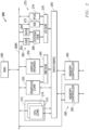
- FIG. 1 illustrates in block diagram form a data processing system 100 according to some embodiments.
- Data processing system 100 includes a data processor 110 in the form of an accelerated processing unit (APU), a memory system 120, a peripheral component interconnect express (PCIe) system 150, a universal serial bus (USB) system 160, and a disk drive 170.
- Data processor 110 operates as the central processing unit (CPU) of data processing system 100 and provides various buses and interfaces useful in modern computer systems. These interfaces include two double data rate (DDRx) memory channels, a PCIe root complex for connection to a PCIe link, a USB controller for connection to a USB network, and an interface to a Serial Advanced Technology Attachment (SATA) mass storage device.
- DDRx double data rate
- PCIe root complex for connection to a PCIe link
- USB controller for connection to a USB network
- SATA Serial Advanced Technology Attachment
- Memory system 120 includes a memory channel 130 and a memory channel 140.
- Memory channel 130 includes a set of dual inline memory modules (DIMMs) connected to a DDRx bus 132, including representative DIMMs 134, 136, and 138 that in this example correspond to separate ranks.
- memory channel 140 includes a set of DIMMs connected to a DDRx bus 142, including representative DIMMs 144, 146, and 148.
- PCIe system 150 includes a PCIe switch 152 connected to the PCIe root complex in data processor 110, a PCIe device 154, a PCIe device 156, and a PCIe device 158.
- PCIe device 156 in turn is connected to a system basic input/output system (BIOS) memory 157.
- BIOS memory 157 can be any of a variety of non-volatile memory types, such as read-only memory (ROM), flash electrically erasable programmable ROM (EEPROM), and the like.
- USB system 160 includes a USB hub 162 connected to a USB master in data processor 110, and representative USB devices 164, 166, and 168 each connected to USB hub 162.
- USB devices 164, 166, and 168 could be devices such as a keyboard, a mouse, a flash EEPROM port, and the like.
- Disk drive 170 is connected to data processor 110 over a SATA bus and provides mass storage for the operating system, application programs, application files, and the like.
- Data processing system 100 is suitable for use in modem computing applications by providing a memory channel 130 and a memory channel 140.
- Each of memory channels 130 and 140 can connect to state-of-the-art DDR memories such as DDR version four (DDR4), low power DDR4 (LPDDR4), graphics DDR version five (gDDR5), and high bandwidth memory (IIBM), and can be adapted for future memory technologies.
- DDR4 DDR version four
- LPDDR4 low power DDR4
- gDDR5 graphics DDR version five
- IIBM high bandwidth memory
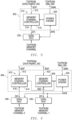
- FIG. 2 illustrates in block diagram form an APU 200 suitable for use in data processing system 100 of FIG. 1 .
- APU 200 includes a central processing unit (CPU) core complex 210, a graphics core 220, a set of display engines 230, a memory management hub 240, a data fabric 250, a set of peripheral controllers 260, a set of peripheral bus controllers 270, a system management unit (SMU) 280, and a set of memory controllers 290.
- CPU central processing unit
- graphics core 220 includes a graphics core 220, a set of display engines 230, a memory management hub 240, a data fabric 250, a set of peripheral controllers 260, a set of peripheral bus controllers 270, a system management unit (SMU) 280, and a set of memory controllers 290.
- SMU system management unit
- CPU core complex 210 includes a CPU core 212 and a CPU core 214.
- CPU core complex 210 includes two CPU cores, but in other embodiments CPU core complex can include an arbitrary number of CPU cores.
- Each of CPU cores 212 and 214 is bidirectionally connected to a system management network (SMN), which forms a control fabric, and to data fabric 250, and is capable of providing memory access requests to data fabric 250.
- SSN system management network
- Each of CPU cores 212 and 214 may be unitary cores, or may further be a core complex with two or more unitary cores sharing certain resources such as caches.
- Graphics core 220 is a high performance graphics processing unit (GPU) capable of performing graphics operations such as vertex processing, fragment processing, shading, texture blending, and the like in a highly integrated and parallel fashion. Graphics core 220 is bidirectionally connected to the SMN and to data fabric 250, and is capable of providing memory access requests to data fabric 250.
- APU 200 may either support a unified memory architecture in which CPU core complex 210 and graphics core 220 share the same memory space, or a memory architecture in which CPU core complex 210 and graphics core 220 share a portion of the memory space, while graphics core 220 also uses a private graphics memory not accessible by CPU core complex 210.
- Display engines 230 render and rasterize objects generated by graphics core 220 for display on a monitor. Graphics core 220 and display engines 230 are bidirectionally connected to a common memory management hub 240 for uniform translation into appropriate addresses in memory system 120, and memory management hub 240 is bidirectionally connected to data fabric 250 for generating such memory accesses and receiving read data returned from the memory system.
- Data fabric 250 includes a crossbar switch for routing memory access requests and memory responses between any memory accessing agent and memory controllers 290. It also includes a system memory map, defined by BIOS, for determining destinations of memory accesses based on the system configuration, as well as buffers for each virtual connection.
- BIOS system memory map
- Peripheral controllers 260 include a USB controller 262 and a SATA interface controller 264, each of which is bidirectionally connected to a system hub 266 and to the SMN bus. These two controllers are merely exemplary of peripheral controllers that may be used in APU 200.
- Peripheral bus controllers 270 include a system controller or "Southbridge” (SB) 272 and a PCIe controller 274, each of which is bidirectionally connected to an input/output (I/O) hub 276 and to the SMN bus.
- I/O hub 276 is also bidirectionally connected to system hub 266 and to data fabric 250.
- a CPU core can program registers in USB controller 262, SATA interface controller 264, SB 272, or PCIe controller 274 through accesses that data fabric 250 routes through I/O hub 276.
- SMU 280 is a local controller that controls the operation of the resources on APU 200 and synchronizes communication among them. SMU 280 manages power-up sequencing of the various processors on APU 200 and controls multiple off-chip devices via reset, enable and other signals. SMU 280 includes one or more clock sources not shown in FIG. 2 , such as a phase locked loop (PLL), to provide clock signals for each of the components of APU 200. SMU 280 also manages power for the various processors and other functional blocks, and may receive measured power consumption values from CPU cores 212 and 214 and graphics core 220 to determine appropriate power states.
- PLL phase locked loop
- APU 200 also implements various system monitoring and power saving functions.
- one system monitoring function is thermal monitoring. For example, if APU 200 becomes hot, then SMU 280 can reduce the frequency and voltage of CPU cores 212 and 214 and/or graphics core 220. If APU 200 becomes too hot, then it can be shut down entirely. Thermal events can also be received from external sensors by SMU 280 via the SMN bus, and SMU 280 can reduce the clock frequency and/or power supply voltage in response.
- FIG. 3 illustrates in block diagram form a memory controller 300 and an associated physical interface (PHY) 330 suitable for use in APU 200 of FIG. 2 according to some embodiments.
- Memory controller 300 includes a memory channel 310 and a power engine 320.
- Memory channel 310 includes a host interface 312, a memory channel controller 314, and a physical interface 316.
- Host interface 312 bidirectionally connects memory channel controller 314 to data fabric 250 over a scalable data port (SDP).
- SDP scalable data port
- Physical interface 316 bidirectionally connects memory channel controller 314 to PHY 330 over a bus that conforms to the DDR-PHY Interface Specification (DFI).
- DFI DDR-PHY Interface Specification
- Power engine 320 is bidirectionally connected to SMU 280 over the SMN bus, to PHY 330 over the Advanced Peripheral Bus (APB), and is also bidirectionally connected to memory channel controller 314.
- PHY 330 has a bidirectional connection to a memory channel such as memory channel 130 or memory channel 140 of FIG. 1 .
- Memory controller 300 is an instantiation of a memory controller for a single memory channel using a single memory channel controller 314, and has a power engine 320 to control operation of memory channel controller 314 in a manner that will be described further below.
- FIG. 4 illustrates in block diagram form another memory controller 400 and associated PHYs 440 and 450 suitable for use in APU 200 of FIG. 2 according to some embodiments.
- Memory controller 400 includes memory channels 410 and 420 and a power engine 430.
- Memory channel 410 includes a host interface 412, a memory channel controller 414, and a physical interface 416.
- Host interface 412 bidirectionally connects memory channel controller 414 to data fabric 250 over an SDP.
- Physical interface 416 bidirectionally connects memory channel controller 414 to PHY 440, and conforms to the DFI Specification.
- Memory channel 420 includes a host interface 422, a memory channel controller 424, and a physical interface 426.
- Host interface 422 bidirectionally connects memory channel controller 424 to data fabric 250 over another SDP.
- Physical interface 426 bidirectionally connects memory channel controller 424 to PHY 450, and conforms to the DFI Specification.
- Power engine 430 is bidirectionally connected to SMU 280 over the SMN bus, to PHYs 440 and 450 over the APB, and is also bidirectionally connected to memory channel controllers 414 and 424.
- PHY 440 has a bidirectional connection to a memory channel such as memory channel 130 of FIG. 1 .
- PHY 450 has a bidirectional connection to a memory channel such as memory channel 140 of FIG. 1 .
- Memory controller 400 is an instantiation of a memory controller having two memory channel controllers and uses a shared power engine 430 to control operation of both memory channel controller 414 and memory channel controller 424 in a manner that will be described further below.
- FIG. 5 illustrates in block diagram form a memory controller 500 according to some embodiments.
- Memory controller 500 includes a memory channel controller 510 and a power controller 550.
- Memory channel controller 510 includes an interface 512, a queue 514, a command queue 520, an address generator 522, a content addressable memory (CAM) 524, a replay queue 530, a refresh logic block 532, a timing block 534, a page table 536, an arbiter 538, an error correction code (ECC) check block 542, an ECC generation block 544, and a data buffer (DB) 546.
- ECC error correction code
- Interface 512 has a first bidirectional connection to data fabric 250 over an external bus, and has an output.
- this external bus is compatible with the advanced extensible interface version four specified by ARM Holdings, PLC of Cambridge, England, known as "AXI4", but can be other types of interfaces in other embodiments.
- Interface 512 translates memory access requests from a first clock domain known as the FCLK (or MEMCLK) domain to a second clock domain internal to memory controller 500 known as the UCLK domain.
- queue 514 provides memory accesses from the UCLK domain to the DFICLK domain associated with the DFI interface.
- Address generator 522 decodes addresses of memory access requests received from data fabric 250 over the AXI4 bus.
- the memory access requests include access addresses in the physical address space represented in a normalized format.
- Address generator 522 converts the normalized addresses into a format that can be used to address the actual memory devices in memory system 120, as well as to efficiently schedule related accesses. This format includes a region identifier that associates the memory access request with a particular rank, a row address, a column address, a bank address, and a bank group.
- the system BIOS queries the memory devices in memory system 120 to determine their size and configuration, and programs a set of configuration registers associated with address generator 522.
- Address generator 522 uses the configuration stored in the configuration registers to translate the normalized addresses into the appropriate format.
- Command queue 520 is a queue of memory access requests received from the memory accessing agents in data processing system 100, such as CPU cores 212 and 214 and graphics core 220.
- Command queue 520 stores the address fields decoded by address generator 522 as well other address information that allows arbiter 538 to select memory accesses efficiently, including access type and quality of service (QoS) identifiers.
- CAM 524 includes information to enforce ordering rules, such as write after write (WAW) and read after write (RAW) ordering rules.
- Replay queue 530 is a temporary queue for storing memory accesses picked by arbiter 538 that are awaiting responses, such as address and command parity responses, write cyclic redundancy check (CRC) responses for DDR4 DRAM or write and read CRC responses for gDDR5 DRAM.
- Replay queue 530 accesses ECC check block 542 to determine whether the returned ECC is correct or indicates an error.
- Replay queue 530 allows the accesses to be replayed in the case of a parity or CRC error of one of these cycles.
- Refresh logic 532 includes state machines for various powerdown, refresh, and termination resistance (ZQ) calibration cycles that are generated separately from normal read and write memory access requests received from memory accessing agents. For example, if a memory rank is in precharge powerdown, it must be periodically awakened to run refresh cycles. Refresh logic 532 generates refresh commands periodically to prevent data errors caused by leaking of charge off storage capacitors of memory cells in DRAM chips. In addition, refresh logic 532 periodically calibrates ZQ to prevent mismatch in on-die termination resistance due to thermal changes in the system.
- ZQ termination resistance
- Arbiter 538 is bidirectionally connected to command queue 520 and is the heart of memory channel controller 510. It improves efficiency by intelligent scheduling of accesses to improve the usage of the memory bus. Arbiter 538 uses timing block 534 to enforce proper timing relationships by determining whether certain accesses in command queue 520 are eligible for issuance based on DRAM timing parameters. For example, each DRAM has a minimum specified time between activate commands, known as "t RC ". Timing block 534 maintains a set of counters that determine eligibility based on this and other timing parameters specified in the JEDEC specification, and is bidirectionally connected to replay queue 530. Page table 536 maintains state information about active pages in each bank and rank of the memory channel for arbiter 538, and is bidirectionally connected to replay queue 530.
- ECC generation block 544 computes an ECC according to the write data.
- DB 546 stores the write data and ECC for received memory access requests. It outputs the combined write data/ECC to queue 514 when arbiter 538 picks the corresponding write access for dispatch to the memory channel.
- Power controller 550 includes an interface 552 to an advanced extensible interface, version one (AXI), an APB interface 554, and a power engine 560.
- Interface 552 has a first bidirectional connection to the SMN, which includes an input for receiving an event signal labeled "EVENT_n" shown separately in FIG. 5 , and an output.
- APB interface 554 has an input connected to the output of interface 552, and an output for connection to a PHY over an APB.
- Power engine 560 has an input connected to the output of interface 552, and an output connected to an input of queue 514.
- Power engine 560 includes a set of configuration registers 562, a microcontroller ( ⁇ C) 564, a self refresh controller (SLFREF/PE) 566, and a reliable read/write timing engine (RRW/TE) 568.
- Configuration registers 562 are programmed over the AXI bus, and store configuration information to control the operation of various blocks in memory controller 500. Accordingly, configuration registers 562 have outputs connected to these blocks that are not shown in detail in FIG. 5 .
- Self refresh controller 566 is an engine that allows the manual generation of refreshes in addition to the automatic generation of refreshes by refresh logic 532.
- Reliable read/write timing engine 568 provides a continuous memory access stream to memory or I/O devices for such purposes as DDR interface maximum read latency (MRL) training and loopback testing.
- MDL maximum read latency
- Memory channel controller 510 includes circuitry that allows it to pick memory accesses for dispatch to the associated memory channel.
- address generator 522 decodes the address information into predecoded information including rank, row address, column address, bank address, and bank group in the memory system, and command queue 520 stores the predecoded information.
- Configuration registers 562 store configuration information to determine how address generator 522 decodes the received address information.
- Arbiter 538 uses the decoded address information, timing eligibility information indicated by timing block 534, and active page information indicated by page table 536 to efficiently schedule memory accesses while observing other criteria such as QoS requirements.
- arbiter 538 implements a preference for accesses to open pages to avoid the overhead of precharge and activation commands required to change memory pages, and hides overhead accesses to one bank by interleaving them with read and write accesses to another bank. In particular during normal operation, arbiter 538 normally keeps pages open in different banks until they are required to be precharged prior to selecting a different page.
- FIG. 6 illustrates in block diagram form a memory controller 600 that can be used to implement a portion of memory controller 500 of FIG. 5 according to some embodiments.
- Memory controller 600 implements address decoder 522 of FIG. 5 as a non power-of-two address decoder 610 to accommodate non-traditional memory sizes.
- memory controller 600 is able to receive the request from data fabric 250 and programmably map it onto non power-of-two memory sizes, such as 6GB DIMMs. This operation will be explained in greater detail below.
- Memory controller 600 has an input port for receiving memory access requests from data fabric 250 using the SDP.
- Each memory access request includes a set of control signals labeled "CONTROL”, a 40-bit address labeled "NORMALIZED ADDRESS", and a set of 256 data signals labeled "DATA".
- CONTROL signals include a tag for the access request, the size of the request, the quality of service requested, the type of access such as read or write, and so on.
- the NORMALIZED ADDRESS includes all of the supported address bits and is a 40-bit address with implied leading zeros appended.
- the DATA signals include a sufficient number of signals that are associated with a single memory access request.
- a CPU core may include a last level cache that has a 256-bit cache line size; thus a writeback of a cache line to memory will require a 256-bit transfer.
- the physical interface such as PHY 330 of FIG. 3 may perform a corresponding memory access as a burst of eight to a 64-bit or 72-bit (64 bits plus 8 bits of error correcting code) DDR DIMM, but the memory controller receives all 256 DATA bits as part of the memory access request.
- Memory controller 600 includes non power-of-two address decoder 610 and write data buffer 546 as previously illustrated in FIG. 5 .
- Address decoder 610 includes an input for receiving the NORMALIZED ADDRESS, and outputs for providing a set of n chip select signals labeled "CS[n]", a set of three chip identification signals labeled "CHIP_ID”, a decoded row address labeled "ROW_ADDRESS”, a decoded column address labeled "COLUMN_ADDRESS”, a bank group signal labeled "BG”, and a bank address signal labeled "BA”.
- Memory controller 600 provides these outputs of address decoder 610 along with the CONTROL signals to command queue 520 to allow command queue 520 to store them so that arbiter 538 can make decisions about the efficient ordering of memory access requests.
- Memory controller 600 also provides the COLUMN_ADDRESS, BG, and BA signals to page table 536 to allow page table 536 to associate access requests with open pages in each DRAM chip.
- Write data buffer 546 is a holding buffer having an input for receiving the 256-bit DATA signal, and an output connected to an input of BEQ 514. Since data fabric 250 provides interspersed read and write memory access requests to memory controller 600, write data buffer 546 will not be used for all received memory access requests but only for writes.
- the system BIOS queries the serial presence detect (SPD) ROM on each memory module of memory channels 130 and 140 at boot-up to determine their respective densities and organizations.
- the system BIOS uses this information to program configurable address decoder registers of address decoder 610 to define the address map for a given workload and memory chip configuration.
- the system BIOS also makes this information available to the operating system to allow it to program page tables used for virtual address translation from logical addresses to physical addresses, which is the format of the NORMALIZED ADDRESS.
- address decoder 610 uses them to decode the NORMALIZED ADDRESS to map each access request to a specific region having a corresponding chip select.
- memory controller 600 also supports a feature known as rank multiplication.
- each packaged integrated circuit on a given DIMM includes a three-dimensional (3D) stack of memory chips interconnected using through-silicon-via (TSV) technology.
- TSV through-silicon-via
- the DDR4 standard specifies a 3-bit chip identification input signal C[2:0] to support stacks of 2, 4, and 8 memory chips. In this way each memory chip in the stack is selected by both a common chip select signal and an encoded C[2:0] signal to identify the selected logical rank within the region.
- address decoder 610 programmably decodes the NORMALIZED ADDRESS into logical ranks and activates a one-hot chip select signal for the selected region and also provides the encoded C[2:0] signal corresponding to the selected logical rank.
- Address decoder 610 supports non power-of-two address decoding. The construction of address decoder 610 will now be described.
- Each region decoder 710 includes a primary decoder 720, a secondary decoder 730, a logic circuit labeled "OR" 740, a first set of configuration registers 750 associated with primary decoder 720 labeled "CFG", and a second set of similarly labeled configuration registers 760 associated with secondary decoder 730.
- configuration registers 750 and 760 are logically associated with primary decoder 720 and secondary decoder 730, respectively, and may either be physically distinct or may be combined with other configuration registers in a central register set such as configuration registers 562 of FIG. 5 .
- Each of configuration registers 750 and 760 has an input connected to the SMN bus, and an output for providing register values for use by a respective one of primary decoder 720 and secondary decoder 730.
- Primary decoder 720 has a first input for receiving the NORMALIZED ADDRESS, a second input connected to the output of configuration registers 750, and an output for providing a primary chip select signal.
- the primary chip select signals are labeled "CSPRI0”, “CSPRI1”, “CSPRI2”, and "CSPRI3", respectively.
- Secondary decoder 730 has a first input for receiving the NORMALIZED ADDRESS, a second input connected to the output of configuration registers 760, and an output for providing a primary chip select signal.
- the primary chip select signals are labeled "CSSEC0”, “CSSEC1”, “CSSEC2”, and “CSSEC3", respectively.
- Logic circuit 740 has a first input connected to the output of primary decoder 720, a second input connected to the output of secondary decoder 730, and an output for providing a respective one of signals "CS0", “CS1”, “CS2”, and "CS3".
- Each set of configuration registers 750 and 760 includes several registers sufficient to define the attributes of the region such that the NORMALIZED ADDRESS can be decoded and mapped to the region.
- a base address register defines the starting address of the region and corresponds to the lowest address in the region
- an address mask register defines the size of the region and thus identifies significant bits to be used in the decoding.
- Each decoder compares the significant bits of the NORMALIZED ADDRESS, masked according to the address mask register, to the corresponding bits of the base address register. If there is a match, then the decoder outputs its respective chip select signal, and logic circuit 740 outputs a final chip select signal. For active high chip select signals, logic circuit 740 is implemented using a logical OR function.
- region decoder 710 supports non power-of-two memory sizes without complicated bit-by-bit decoding, thereby reducing the size of the decoders. Since each of the primary and secondary decoders have a power-of-two size, they can perform region decoding on a subset of the NORMALIZED ADDRESS bits quickly and efficiently using a compact circuit. By reducing the number of bits required in the decoding operation, address decoder 700 is able to decode addresses faster. For example a full bit-by-bit comparison of 32 bits of the 40-bit NORMALIZED ADDRESS to base and limit registers of an arbitrary region size would require more than a single clock cycle to resolve for higher clock rates using contemporary CMOS logic processes.
- each address decoder could include a primary decoder, a secondary decoder, and a tertiary decoder that have respective sizes of 2 N , 2 (N-1) , and 2 (N-2) .
- N is equal to 32
- this configuration allows the decoding of normalized addresses into region sizes of and of 1-7GB in 1GB increments. This concept could be further extended to four or more decoders as well.
- FIG. 8 illustrates a diagram 800 showing the address mapping performed by the address decoder of FIG. 7 when programmed for a non-power-of-two address space using two region decoders.
- Diagram 800 includes a normalized address space 810, a first region 820, and a second region 830.
- Normalized address space 810 has a 4GB sub-region 812 associated with decoded signal CSPRI0, a 4GB sub-region 814 associated with decoder signal CSPRI1, a 2GB sub-region 816 associated with decoded signal CSSEC0, and a 2GB sub-region associated with decoded signal CSSEC1.
- Sub-region 812 starts at address 0x0 and extends to address 0x0_FFFF_FFFF, which is 4G - 1 (2 32 - 1), in which 0x indicates a 40-bit hexadecimal address with implied leading zeros.
- Sub-region 814 starts at address 0x1_0000_0000 (2 32 ) and extends to address 0x1_FFFF_FFFF, which is 8G - 1 (2 32 + 2 32 - 1).
- Sub-region 816 starts at address 0x2_0000_0000 (8G) and extends to address 0x2_7FFF_FFFF (10G - 1).
- Sub-region 818 starts at address 0x2_8000_0000 (10G) and extends to address 0x2_FFFF_FFFF (12G - 1).
- First region 820 is a 6GB region associated with CS0 and has a 4GB primary portion 822 and a 2GB secondary portion 824.
- First region 820 is implemented with 48K (49,152) rows of 128K (131,072) bytes each, in which a primary region 822 is implemented with 32K (32,768) rows extending from row address 0x0 to row address 0x7FFF, and a secondary region 824 is implemented with 16K rows extending from row address 0x8000 to 0xbFFF.
- second region 830 is implemented with 48K rows of 128K bytes each, in which a primary region 832 is implemented with 32K rows extending from row address 0x0 to row address 0x7FFF, and a secondary region 834 is implemented with 16K rows extending from row address 0x8000 to 0xbFFF.
- the system BIOS programs configuration registers as shown in TABLE II: TABLE II Register Name Register Function Value BaseAddrCS0[39:8] Base address register for CS0 primary decoder 0x0_0000_00 BaseAddrCS1[39:8] Base address register for CS1 primary decoder 0x1_0000_00 BaseAddrSecCS0[39:8] Base address register for CS0 secondary decoder 0x2_0000_00 BaseAddrSecCS1[39:8] Base address register for CS1 secondary decoder 0x2_8000_00 AddrMaskCS01[39:8] Address mask for primary decoders for CS0 and CS 1 0x0_FFFF_FF AddrMaskSecCS01[39:8] Address mask for secondary decoders for CS0 and CS1 0x0_7FFF_FF Note that bits [7:0] represent byte addressing of 256 bytes. These bits are dropped
- bank swizzle mode in which certain bits of the input address are decoded to form the bank address. These particular bits include certain bits of the access address such as low-order row address bits to generate new bank (or in the case of DDR4 both bank and bank group) bits. In this way different portions of a set of contiguous addresses that would have otherwise caused page conflicts are divided between banks, resulting in greater efficiency.
- a memory controller as described herein includes programmable mechanisms to interleave the physical address space across a set of distinct regions.
- a memory controller as described above for example memory controller 292 or 294 of FIG. 2 or memory controller 500 of FIG. 5 , can operate more efficiently by spreading a series of accesses that may be encountered during execution of a program across multiple ranks of DRAM.
- overhead cycles such as page precharges and page activates can be hidden within useful cycles.
- the first mechanism is chip select interleaving that can be accomplished using the primary and secondary region decoders.
- FIG. 9 illustrates a diagram 900 showing the address mapping performed by the address decoder of FIG. 7 when programmed to implement chip select interleave using two address decoders according to some embodiments.
- Diagram 900 includes a normalized address space 910, a first region 920, and a second region 930.
- Normalized address space 910 has a 2GB sub-region 912 associated with decoded signal CSPRI0, a 2GB sub-region 914 associated with decoder signal CSPRI1, a 2GB sub-region 916 associated with decoded signal CSSEC0, and a 2GB sub-region 918 associated with decoded signal CSSEC1.
- Sub-region 912 starts at address 0x0 and extends to address 0x0_7FFF_FFFF, which is 2G - 1 (2 31 - 1).
- Sub-region 914 starts at address 0x8_0000_0000 (2 31 ) and extends to address 0x0_FFFF_FFFF, which is 4G - 1 (2 31 + 2 31 - 1).
- Sub-region 916 starts at address 0x1_0000_0000 (4GB) and extends to address 0x1_7FFF_FF (6G - 1).
- Sub-region 918 starts at address 0x1_8000_0000 (6G) and extends to address 0x1_FFFF_FFFF (8G - 1).
- chip select interleave In the chip select interleave mode, memory controller 600 interleaves the physical address space over multiple DIMM ranks on a channel, as opposed to a single DIMM rank occupying a contiguous set of addresses in the normalized address space.
- Chip select (CS) interleave reduces page conflicts as potentially more DRAM banks can be used over a smaller address region, effectively making more DRAM banks available.
- the number of interleaved chip select signals is a power of two.
- the regions are the same size. In the example in FIG. 9 , there are two (2 1 ) chip selects for two regions having the same size (4GB).
- address bit A[12] (corresponding to a size of 1024 KB) was mapped to column address bit 9 (COL[9]).
- This mapping allows the firmware additional flexibility when implementing interleaving.
- A[12] is used for CS interleaving, and COL[9] is mapped instead to A[13], and higher order address bits are used for bank and bank group addresses, namely A[14] for BA0, A[15] for BA1, etc. according to the pattern of TABLE I.
- Hashing provides a finer granularity by allowing more address bits to be used.
- the number and location of the address bits used in hashing can be programmed by the user, providing flexibility so that the hashing operation can be tailored for the specific application and the characteristics of the software code.
- FIG. 10 illustrates in block diagram form a portion of a memory controller 1000 that can be used to implement address decoder 522 of FIG. 5 according to some embodiments.
- Memory controller 1000 includes an address decoder 1010 and a set of configuration registers 1020.
- Address decoder 1010 includes a chip select (CS) hashing circuit 1012 and a bank address (BA) hashing circuit 1014.
- CS hashing circuit 1012 has an input for receiving the 40-bit NORMALIZED ADDRESS from interface 512, and an output for providing a set of hashed chip select signals labeled "CS_HASH".
- BA hashing circuit 1014 has a first input connected to the output of CS hashing circuit 1012, a second input for receiving the NORMALIZED ADDRESS, and outputs for providing the CHIP_ID, ROW_ADDRESS, COLUMN_ADDRESS, BG, and BA_HASH signals.
- Memory controller 1000 provides decoded memory accesses using these outputs along with the CONTROL signals to command queue 520 to allow command queue 520 to store them so that arbiter 538 can make decisions about the efficient ordering of memory access requests.
- Address decoder 1010 receives fields from various configuration registers for the base address and size of each memory chip in the memory channel as described above.
- address decoder 1010 uses additional configuration registers to support a programmable hashing function, and FIG. 10 shows only these additional configuration registers.
- address decoder 1010 supports up to four chip select signals and up to thirty-two banks.
- configuration registers 1020 include a set of two CS hash registers 1030 each corresponding to a bit of the encoded CS signal, and a set of five BA hash registers 1040, each corresponding to a bit of the encoded BA signal.
- CS hash registers 1030 include a first CS hash register 1032 associated with CS_HASH[0] and a second CS hash register 1034 associated with CS_HASH[1].
- Each CS hash register is a 32-bit register that includes a 30-bit field labeled "NORMALIZED ADDRESS XOR[39:9]" in register bits 31:1 and an enable field labeled "EN" in register bit 0.
- BA hash registers 1040 include BA hash registers 1042, 1044, 1046, 1048, and 1050 associated with hashed bank address bits BA_HASH[0], BA_HASH[1], BA_HASH[2], BA_HASH[3], and BA_HASH[4], respectively.
- Each BA hash register is a thirty-two bit register with three fields: an 18-bit row exclusive-OR (XOR) field labeled "ROWXOR[17:0]” in register bits 31:14, a 13-bit column XOR field labeled "COLXOR[12:0]” in register bits 13:1, and an enable field labeled "EN" in register bit 0.
- XOR row exclusive-OR
- Address decoder 1010 performs bitwise XOR operations using selected bits of the NORMALIZED ADDRESS.
- CS hashing circuit 1012 first hashes the chip select bits using selected ones of the most significant thirty-one bits of the NORMALIZED ADDRESS.
- Each bit of the NORMALIZED ADDRESS XOR field of the CS hash register is used to selectively perform a bitwise exclusive OR (XOR) operation on the indicated bits of the NORMALIZED ADDRESS.
- CS_HASH 0 CS 0 ⁇ CS 0 _XORENABLE & ⁇ NORMADDR 39 : 9 & CS 0 _NORMADDRXOR
- CS_HASH 1 CS 1 ⁇ CS 1 _XORENABLE & ⁇ NORMADDR 39 : 9 & CS 1 _NORMADDRXOR in which ⁇ represents the XOR operator, and ⁇ () represents the bitwise XOR operator on respective pairs of bits.
- the CS and BA hashing functions can be extended to additional levels of memory organization.
- HBM memories implement a concept known as a "pseudo channel".
- the pseudo channel can be also hashed using a corresponding hashing equation and a corresponding pseudo channel register, as described in Equation [8] below:
- PC_HASH PC ⁇ (PC_XORENABLE & ( ⁇ (COL[12:0] & PC_COLXOR)) ⁇ ( ⁇ (ROW[17:0] & PC_ROWXOR)) ⁇ ( ⁇ (BANK[4:0] & PC_BANKXOR))
- the memory controller uses an additional hashing circuit and an additional configuration register.
- the hashing algorithm is programmable through a set of hashing registers that can be selectively programmed by the system BIOS.
- FIG. 11 illustrates in block diagram form another portion of a memory controller 1100 that can be used to implement address decoder 522 of FIG. 5 according to some embodiments.
- memory controller 1100 includes an address decoder 1110 having a hashing circuit 1120 followed by a non-power-of-two decoder 1130.
- Hashing circuit 1120 has an input for receiving an access address and an output and can be implemented with hashing circuit 1010 of FIG. 10 .
- Non-power-of-two decoder 1130 has an input connected to the output of hashing circuit 1120, and an output for providing a decoded address, and can be implemented with non-power-of-two decoder circuit 610 of FIGs. 6 and 7 .
- Memory controller 1100 illustrates that not only can the hashing mechanism and the non-power-of-two memory size decoder be implemented separately, they also can be used together in a single memory decoder 1110. In this case, the hashing mechanism seamlessly precedes the non-power-of-two decoding to provide a memory controller with further enhanced flexibility by supporting both functions.
- the hashing operation can also be used seamlessly with non power-of-two memory sizes.
- the way in which hashing circuit 1012 performs the hashing operation with a non-power-of-two memory address size can be described with respect to a particular example.
- a dual-rank 12 Gb memory is implemented using two region decoders, in which the first region decoder for CS0 maps to 12 Gb of the memory space using a primary decoder (CS0p) and a secondary decoder (CS0s), and a second region decoder for CS1 maps to 12 Gb of the memory space using a primary decoder (CS1p) and a secondary decoder (CS1s).
- non-power-of-two decoder 1130 When the system BIOS configures non-power-of-two decoder 1130 to set up a non-power-of-two size, there is an additional restriction on the hashing function due to the DRAM architecture. For example according to the configuration illustrated in FIGs. 8 and 9 , there are only 48K rows, and the ROWXOR bits corresponding to Row[MSB:MSB-1] should not be enabled for the hashing operation because it would not correctly translate the three states into the correct number of bank states. Instead these bits can only be used in memories with a power-of-two size.
- the memory controller described above is able to perform flexible address mapping through a variety of configurable options, providing the user a range of choices.
- address mapping choices include support for non power-of-two memory sizes, interleaving, and hashing, all of which are implemented in one combined decoder (address decoder 522).
- Memory controller 500 of FIG. 5 or address decoder 610 of FIG. 6 or any portions thereof may be described or represented by a computer accessible data structure in the form of a database or other data structure which can be read by a program and used, directly or indirectly, to fabricate integrated circuits.
- this data structure may be a behavioral-level description or register-transfer level (RTL) description of the hardware functionality in a high level design language (HDL) such as Verilog or VHDL.
- HDL high level design language
- VHDL Verilog or VHDL
- the description may be read by a synthesis tool which may synthesize the description to produce a netlist comprising a list of gates from a synthesis library.
- the netlist includes a set of gates that also represent the functionality of the hardware comprising integrated circuits.
- the netlist may then be placed and routed to produce a data set describing geometric shapes to be applied to masks.
- the masks may then be used in various semiconductor fabrication steps to produce the integrated circuits.
- the database on the computer accessible storage medium may be the netlist (with or without the synthesis library) or the data set, as desired, or Graphic Data System (GDS) IIdata.
- GDS Graphic Data System
- memory controller 500 may interface to other types of memory besides DDRx memory, such as high bandwidth memory (HBM), RAMbus DRAM (RDRAM), and the like as well as different types of DIMMs.
- memory controller 500 is scalable to access memories of different sizes. The number of power-of-two decoders will vary in other embodiments. While the illustrated embodiment described memory addressing and control signals useful in DDR memory, they will vary depending on the type of memory used.
- exemplary data processing system 100 was based on an APU having both CPU cores and GPU cores, such as APU 200 of FIG. 2 , but the techniques described above also apply to CPUs (systems with one or more CPU cores but no GPU cores) and GPUs (systems with no CPU cores but one or more GPU cores).
Landscapes
- Engineering & Computer Science (AREA)
- Theoretical Computer Science (AREA)
- General Engineering & Computer Science (AREA)
- Physics & Mathematics (AREA)
- General Physics & Mathematics (AREA)
- Computer Hardware Design (AREA)
- Microelectronics & Electronic Packaging (AREA)
- Memory System (AREA)
- Dram (AREA)
- Techniques For Improving Reliability Of Storages (AREA)
- Power Sources (AREA)
- Bus Control (AREA)
Applications Claiming Priority (2)
| Application Number | Priority Date | Filing Date | Title |
|---|---|---|---|
| US15/211,887 US10403333B2 (en) | 2016-07-15 | 2016-07-15 | Memory controller with flexible address decoding |
| PCT/US2016/053358 WO2018013158A1 (en) | 2016-07-15 | 2016-09-23 | Memory controller with flexible address decoding |
Publications (3)
| Publication Number | Publication Date |
|---|---|
| EP3485383A1 EP3485383A1 (en) | 2019-05-22 |
| EP3485383A4 EP3485383A4 (en) | 2020-04-22 |
| EP3485383B1 true EP3485383B1 (en) | 2025-04-02 |
Family
ID=60940724
Family Applications (1)
| Application Number | Title | Priority Date | Filing Date |
|---|---|---|---|
| EP16909049.5A Active EP3485383B1 (en) | 2016-07-15 | 2016-09-23 | Memory controller with flexible address decoding |
Country Status (6)
| Country | Link |
|---|---|
| US (1) | US10403333B2 (enExample) |
| EP (1) | EP3485383B1 (enExample) |
| JP (1) | JP6761891B2 (enExample) |
| KR (1) | KR102719994B1 (enExample) |
| CN (1) | CN109478169B (enExample) |
| WO (1) | WO2018013158A1 (enExample) |
Families Citing this family (30)
| Publication number | Priority date | Publication date | Assignee | Title |
|---|---|---|---|---|
| EP3534264B1 (en) * | 2016-11-23 | 2024-05-22 | Huawei Technologies Co., Ltd. | Memory allocation method and apparatus |
| US11082523B2 (en) * | 2017-02-09 | 2021-08-03 | International Business Machines Corporation | System, method and computer program product for a distributed virtual address space |
| IT201800002895A1 (it) | 2018-02-21 | 2019-08-21 | Stmicroelectronics Application Gmbh | Sistema di elaborazione, relativo circuito integrato, dispositivo e procedimento |
| KR102583448B1 (ko) * | 2018-04-10 | 2023-09-27 | 에스케이하이닉스 주식회사 | 온도 관리를 위해 주소를 제어하는 반도체 메모리 장치 |
| US11194382B2 (en) * | 2018-10-16 | 2021-12-07 | Advanced Micro Devices, Inc. | Speculative exit from power down mode of a dynamic random access memory rank |
| US10642734B1 (en) * | 2018-12-03 | 2020-05-05 | Advanced Micro Devices, Inc. | Non-power of two memory configuration |
| KR102849285B1 (ko) | 2019-09-20 | 2025-08-25 | 삼성전자주식회사 | 메모리 모듈, 그것을 제어하는 메모리 제어기의 에러 정정 방법, 및 그것을포함하는 컴퓨팅 시스템 |
| US11403217B2 (en) * | 2019-10-30 | 2022-08-02 | Qualcomm Incorporated | Memory bank group interleaving |
| US11537319B2 (en) * | 2019-12-11 | 2022-12-27 | Advanced Micro Devices, Inc. | Content addressable memory with sub-field minimum and maximum clamping |
| US11561862B2 (en) | 2020-05-29 | 2023-01-24 | Advanced Micro Devices, Inc. | Refresh management for DRAM |
| CN112286844B (zh) * | 2020-10-30 | 2022-09-02 | 烽火通信科技股份有限公司 | 一种可适配业务地址映射的ddr4控制方法及装置 |
| CN115132245B (zh) * | 2021-03-29 | 2026-03-03 | 深圳富联富桂精密工业有限公司 | 级联前端控制器的寻址装置及上行发送功率确定方法 |
| US11379388B1 (en) * | 2021-03-31 | 2022-07-05 | Advanced Micro Devices, Inc. | Credit scheme for multi-queue memory controllers |
| US11972140B2 (en) | 2021-04-26 | 2024-04-30 | Apple Inc. | Hashing with soft memory folding |
| US12236130B2 (en) | 2021-04-26 | 2025-02-25 | Apple Inc. | Address hashing in a multiple memory controller system |
| US11714571B2 (en) | 2021-04-26 | 2023-08-01 | Apple Inc. | Address bit dropping to create compacted pipe address for a memory controller |
| CN113312277B (zh) * | 2021-06-29 | 2024-06-25 | 合肥忆芯电子科技有限公司 | 存储体地址映射装置、方法及电子设备 |
| JP7168731B1 (ja) | 2021-07-19 | 2022-11-09 | Necプラットフォームズ株式会社 | メモリアクセス制御装置、メモリアクセス制御方法、及び、メモリアクセス制御プログラム |
| US11934313B2 (en) | 2021-08-23 | 2024-03-19 | Apple Inc. | Scalable system on a chip |
| US12386735B2 (en) * | 2021-09-22 | 2025-08-12 | Intel Corporation | Software driven dynamic memory allocation and address mapping for disaggregated memory pool |
| CN116226023A (zh) * | 2021-12-02 | 2023-06-06 | 平头哥(上海)半导体技术有限公司 | 并行处理单元、处理系统以及相关方法 |
| US12117945B2 (en) * | 2022-06-24 | 2024-10-15 | Advanced Micro Devices, Inc. | Memory controller with pseudo-channel support |
| US12050532B2 (en) * | 2022-09-23 | 2024-07-30 | Apple Inc. | Routing circuit for computer resource topology |
| CN116049047B (zh) * | 2022-12-30 | 2024-04-12 | 成都电科星拓科技有限公司 | 一种eeprom访问方法 |
| US12380019B2 (en) | 2023-03-21 | 2025-08-05 | Qualcomm Incorporated | System memory address decoding for interleaving addresses across physical regions of a system-on-chip (SOC) and across shared memory resources in a processor-based system |
| WO2024196846A1 (en) * | 2023-03-21 | 2024-09-26 | Qualcomm Incorporated | System memory address decoding for interleaving addresses across physical regions of a system-on-chip (soc) and across shared memory resources in a processor-based system |
| CN116700631B (zh) * | 2023-08-03 | 2023-09-29 | 摩尔线程智能科技(北京)有限责任公司 | 任务管理装置、方法、图形处理器及电子设备 |
| US12504878B1 (en) * | 2023-11-07 | 2025-12-23 | Google Llc | Mechanism for efficient accessing to memory controllers with non-power-of-two sized memory |
| US20250348235A1 (en) * | 2024-05-09 | 2025-11-13 | Qualcomm Incorporated | Slice-based memory channel power control |
| CN118571297B (zh) * | 2024-07-17 | 2024-10-29 | 深圳鲲云信息科技有限公司 | 一种存储电路的验证方法及计算设备 |
Citations (1)
| Publication number | Priority date | Publication date | Assignee | Title |
|---|---|---|---|---|
| US20150221358A1 (en) * | 2014-02-03 | 2015-08-06 | Advanced Micro Devices, Inc. | Memory and memory controller for high reliability operation and method |
Family Cites Families (21)
| Publication number | Priority date | Publication date | Assignee | Title |
|---|---|---|---|---|
| US5142672A (en) * | 1987-12-15 | 1992-08-25 | Advanced Micro Devices, Inc. | Data transfer controller incorporating direct memory access channels and address mapped input/output windows |
| DE3883389T2 (de) * | 1988-10-28 | 1994-03-17 | Ibm | Zweistufige Adressendekodierschaltung für Halbleiterspeicher. |
| JPH0684370A (ja) * | 1992-09-01 | 1994-03-25 | Nec Corp | 半導体スタティック・メモリ |
| US5748939A (en) * | 1993-06-30 | 1998-05-05 | Intel Corporation | Memory device with a central control bus and a control access register for translating an access request into an access cycle on the central control bus |
| KR100338791B1 (ko) * | 1993-07-15 | 2002-11-02 | 썬 마이크로시스템즈, 인코포레이티드 | 워드라인디코더/드라이버회로및방법 |
| JP3713312B2 (ja) * | 1994-09-09 | 2005-11-09 | 株式会社ルネサステクノロジ | データ処理装置 |
| US5764963A (en) * | 1995-07-07 | 1998-06-09 | Rambus, Inc. | Method and apparatus for performing maskable multiple color block writes |
| US7318114B1 (en) | 2004-10-29 | 2008-01-08 | Sun Microsystems, Inc. | System and method for dynamic memory interleaving and de-interleaving |
| US7480781B2 (en) | 2004-12-30 | 2009-01-20 | Intel Corporation | Apparatus and method to merge and align data from distributed memory controllers |
| JP2006268905A (ja) * | 2005-03-22 | 2006-10-05 | Matsushita Electric Ind Co Ltd | 半導体記憶回路、半導体記憶回路の構成方法、及び、半導体記憶回路のレイアウト生成方法 |
| US9171585B2 (en) * | 2005-06-24 | 2015-10-27 | Google Inc. | Configurable memory circuit system and method |
| US7620793B1 (en) * | 2006-08-28 | 2009-11-17 | Nvidia Corporation | Mapping memory partitions to virtual memory pages |
| JP5018074B2 (ja) * | 2006-12-22 | 2012-09-05 | 富士通セミコンダクター株式会社 | メモリ装置,メモリコントローラ及びメモリシステム |
| JP2009015832A (ja) * | 2007-06-07 | 2009-01-22 | Renesas Technology Corp | アクセス間調停回路、半導体装置およびアクセス間調停方法 |
| US8438320B2 (en) * | 2007-06-25 | 2013-05-07 | Sonics, Inc. | Various methods and apparatus for address tiling and channel interleaving throughout the integrated system |
| US7793038B2 (en) * | 2007-06-26 | 2010-09-07 | International Business Machines Corporation | System and method for programmable bank selection for banked memory subsystems |
| US7813212B2 (en) * | 2008-01-17 | 2010-10-12 | Mosaid Technologies Incorporated | Nonvolatile memory having non-power of two memory capacity |
| US20120137090A1 (en) * | 2010-11-29 | 2012-05-31 | Sukalpa Biswas | Programmable Interleave Select in Memory Controller |
| US9432298B1 (en) * | 2011-12-09 | 2016-08-30 | P4tents1, LLC | System, method, and computer program product for improving memory systems |
| US9141541B2 (en) | 2013-09-20 | 2015-09-22 | Advanced Micro Devices, Inc. | Nested channel address interleaving |
| US9213600B2 (en) | 2013-11-11 | 2015-12-15 | Seagate Technology Llc | Dynamic per-decoder control of log likelihood ratio and decoding parameters |
-
2016
- 2016-07-15 US US15/211,887 patent/US10403333B2/en active Active
- 2016-09-23 KR KR1020197002561A patent/KR102719994B1/ko active Active
- 2016-09-23 WO PCT/US2016/053358 patent/WO2018013158A1/en not_active Ceased
- 2016-09-23 JP JP2019500870A patent/JP6761891B2/ja active Active
- 2016-09-23 EP EP16909049.5A patent/EP3485383B1/en active Active
- 2016-09-23 CN CN201680087529.9A patent/CN109478169B/zh active Active
Patent Citations (1)
| Publication number | Priority date | Publication date | Assignee | Title |
|---|---|---|---|---|
| US20150221358A1 (en) * | 2014-02-03 | 2015-08-06 | Advanced Micro Devices, Inc. | Memory and memory controller for high reliability operation and method |
Also Published As
| Publication number | Publication date |
|---|---|
| EP3485383A1 (en) | 2019-05-22 |
| WO2018013158A1 (en) | 2018-01-18 |
| US10403333B2 (en) | 2019-09-03 |
| CN109478169B (zh) | 2023-07-28 |
| JP6761891B2 (ja) | 2020-09-30 |
| EP3485383A4 (en) | 2020-04-22 |
| KR102719994B1 (ko) | 2024-10-22 |
| CN109478169A (zh) | 2019-03-15 |
| US20180019006A1 (en) | 2018-01-18 |
| JP2019520660A (ja) | 2019-07-18 |
| KR20190019200A (ko) | 2019-02-26 |
Similar Documents
| Publication | Publication Date | Title |
|---|---|---|
| EP3485383B1 (en) | Memory controller with flexible address decoding | |
| US11221772B2 (en) | Self refresh state machine mop array | |
| CN115516563B (zh) | 用于dram的刷新管理 | |
| KR102714770B1 (ko) | 저 전력 메모리 스로틀링 | |
| CN109564556B (zh) | 具有条纹和读取/写入事务管理的存储器控制器仲裁器 | |
| US10037150B2 (en) | Memory controller with virtual controller mode | |
| WO2018013157A1 (en) | Command arbitration for high speed memory interfaces | |
| KR102871204B1 (ko) | 완전한 동적 포스트-패키지 리페어 | |
| EP3270295A1 (en) | Memory controller with virtual controller mode |
Legal Events
| Date | Code | Title | Description |
|---|---|---|---|
| STAA | Information on the status of an ep patent application or granted ep patent |
Free format text: STATUS: THE INTERNATIONAL PUBLICATION HAS BEEN MADE |
|
| PUAI | Public reference made under article 153(3) epc to a published international application that has entered the european phase |
Free format text: ORIGINAL CODE: 0009012 |
|
| STAA | Information on the status of an ep patent application or granted ep patent |
Free format text: STATUS: REQUEST FOR EXAMINATION WAS MADE |
|
| 17P | Request for examination filed |
Effective date: 20190129 |
|
| AK | Designated contracting states |
Kind code of ref document: A1 Designated state(s): AL AT BE BG CH CY CZ DE DK EE ES FI FR GB GR HR HU IE IS IT LI LT LU LV MC MK MT NL NO PL PT RO RS SE SI SK SM TR |
|
| AX | Request for extension of the european patent |
Extension state: BA ME |
|
| DAV | Request for validation of the european patent (deleted) | ||
| DAX | Request for extension of the european patent (deleted) | ||
| A4 | Supplementary search report drawn up and despatched |
Effective date: 20200323 |
|
| RIC1 | Information provided on ipc code assigned before grant |
Ipc: G06F 13/16 20060101AFI20200317BHEP Ipc: G06F 13/40 20060101ALI20200317BHEP Ipc: G06F 12/02 20060101ALI20200317BHEP |
|
| STAA | Information on the status of an ep patent application or granted ep patent |
Free format text: STATUS: EXAMINATION IS IN PROGRESS |
|
| 17Q | First examination report despatched |
Effective date: 20211115 |
|
| REG | Reference to a national code |
Ref country code: DE Ref legal event code: R079 Free format text: PREVIOUS MAIN CLASS: G06F0013160000 Ipc: G06F0012101800 Ref country code: DE Ref legal event code: R079 Ref document number: 602016091800 Country of ref document: DE Free format text: PREVIOUS MAIN CLASS: G06F0013160000 Ipc: G06F0012101800 |
|
| RIC1 | Information provided on ipc code assigned before grant |
Ipc: G06F 12/14 20060101ALI20231209BHEP Ipc: G06F 12/06 20060101ALI20231209BHEP Ipc: G11C 7/10 20060101ALI20231209BHEP Ipc: G06F 12/1018 20160101AFI20231209BHEP |
|
| GRAP | Despatch of communication of intention to grant a patent |
Free format text: ORIGINAL CODE: EPIDOSNIGR1 |
|
| STAA | Information on the status of an ep patent application or granted ep patent |
Free format text: STATUS: GRANT OF PATENT IS INTENDED |
|
| INTG | Intention to grant announced |
Effective date: 20241028 |
|
| GRAS | Grant fee paid |
Free format text: ORIGINAL CODE: EPIDOSNIGR3 |
|
| GRAA | (expected) grant |
Free format text: ORIGINAL CODE: 0009210 |
|
| STAA | Information on the status of an ep patent application or granted ep patent |
Free format text: STATUS: THE PATENT HAS BEEN GRANTED |
|
| AK | Designated contracting states |
Kind code of ref document: B1 Designated state(s): AL AT BE BG CH CY CZ DE DK EE ES FI FR GB GR HR HU IE IS IT LI LT LU LV MC MK MT NL NO PL PT RO RS SE SI SK SM TR |
|
| REG | Reference to a national code |
Ref country code: GB Ref legal event code: FG4D |
|
| REG | Reference to a national code |
Ref country code: CH Ref legal event code: EP |
|
| P01 | Opt-out of the competence of the unified patent court (upc) registered |
Free format text: CASE NUMBER: APP_12088/2025 Effective date: 20250312 |
|
| REG | Reference to a national code |
Ref country code: IE Ref legal event code: FG4D |
|
| REG | Reference to a national code |
Ref country code: DE Ref legal event code: R096 Ref document number: 602016091800 Country of ref document: DE |
|
| REG | Reference to a national code |
Ref country code: NL Ref legal event code: MP Effective date: 20250402 |
|
| PG25 | Lapsed in a contracting state [announced via postgrant information from national office to epo] |
Ref country code: NL Free format text: LAPSE BECAUSE OF FAILURE TO SUBMIT A TRANSLATION OF THE DESCRIPTION OR TO PAY THE FEE WITHIN THE PRESCRIBED TIME-LIMIT Effective date: 20250402 |
|
| REG | Reference to a national code |
Ref country code: AT Ref legal event code: MK05 Ref document number: 1781946 Country of ref document: AT Kind code of ref document: T Effective date: 20250402 |
|
| PG25 | Lapsed in a contracting state [announced via postgrant information from national office to epo] |
Ref country code: PT Free format text: LAPSE BECAUSE OF FAILURE TO SUBMIT A TRANSLATION OF THE DESCRIPTION OR TO PAY THE FEE WITHIN THE PRESCRIBED TIME-LIMIT Effective date: 20250804 Ref country code: ES Free format text: LAPSE BECAUSE OF FAILURE TO SUBMIT A TRANSLATION OF THE DESCRIPTION OR TO PAY THE FEE WITHIN THE PRESCRIBED TIME-LIMIT Effective date: 20250402 Ref country code: FI Free format text: LAPSE BECAUSE OF FAILURE TO SUBMIT A TRANSLATION OF THE DESCRIPTION OR TO PAY THE FEE WITHIN THE PRESCRIBED TIME-LIMIT Effective date: 20250402 |
|
| PGFP | Annual fee paid to national office [announced via postgrant information from national office to epo] |
Ref country code: DE Payment date: 20250819 Year of fee payment: 10 |
|
| REG | Reference to a national code |
Ref country code: LT Ref legal event code: MG9D |
|
| PG25 | Lapsed in a contracting state [announced via postgrant information from national office to epo] |
Ref country code: NO Free format text: LAPSE BECAUSE OF FAILURE TO SUBMIT A TRANSLATION OF THE DESCRIPTION OR TO PAY THE FEE WITHIN THE PRESCRIBED TIME-LIMIT Effective date: 20250702 Ref country code: GR Free format text: LAPSE BECAUSE OF FAILURE TO SUBMIT A TRANSLATION OF THE DESCRIPTION OR TO PAY THE FEE WITHIN THE PRESCRIBED TIME-LIMIT Effective date: 20250703 |
|
| PG25 | Lapsed in a contracting state [announced via postgrant information from national office to epo] |
Ref country code: PL Free format text: LAPSE BECAUSE OF FAILURE TO SUBMIT A TRANSLATION OF THE DESCRIPTION OR TO PAY THE FEE WITHIN THE PRESCRIBED TIME-LIMIT Effective date: 20250402 |
|
| PG25 | Lapsed in a contracting state [announced via postgrant information from national office to epo] |
Ref country code: BG Free format text: LAPSE BECAUSE OF FAILURE TO SUBMIT A TRANSLATION OF THE DESCRIPTION OR TO PAY THE FEE WITHIN THE PRESCRIBED TIME-LIMIT Effective date: 20250402 |
|
| PGFP | Annual fee paid to national office [announced via postgrant information from national office to epo] |
Ref country code: GB Payment date: 20250911 Year of fee payment: 10 |
|
| PG25 | Lapsed in a contracting state [announced via postgrant information from national office to epo] |
Ref country code: HR Free format text: LAPSE BECAUSE OF FAILURE TO SUBMIT A TRANSLATION OF THE DESCRIPTION OR TO PAY THE FEE WITHIN THE PRESCRIBED TIME-LIMIT Effective date: 20250402 |
|
| PG25 | Lapsed in a contracting state [announced via postgrant information from national office to epo] |
Ref country code: AT Free format text: LAPSE BECAUSE OF FAILURE TO SUBMIT A TRANSLATION OF THE DESCRIPTION OR TO PAY THE FEE WITHIN THE PRESCRIBED TIME-LIMIT Effective date: 20250402 |
|
| PG25 | Lapsed in a contracting state [announced via postgrant information from national office to epo] |
Ref country code: RS Free format text: LAPSE BECAUSE OF FAILURE TO SUBMIT A TRANSLATION OF THE DESCRIPTION OR TO PAY THE FEE WITHIN THE PRESCRIBED TIME-LIMIT Effective date: 20250702 |
|
| PG25 | Lapsed in a contracting state [announced via postgrant information from national office to epo] |
Ref country code: IS Free format text: LAPSE BECAUSE OF FAILURE TO SUBMIT A TRANSLATION OF THE DESCRIPTION OR TO PAY THE FEE WITHIN THE PRESCRIBED TIME-LIMIT Effective date: 20250802 |
|
| PG25 | Lapsed in a contracting state [announced via postgrant information from national office to epo] |
Ref country code: LV Free format text: LAPSE BECAUSE OF FAILURE TO SUBMIT A TRANSLATION OF THE DESCRIPTION OR TO PAY THE FEE WITHIN THE PRESCRIBED TIME-LIMIT Effective date: 20250402 |
|
| REG | Reference to a national code |
Ref country code: DE Ref legal event code: R097 Ref document number: 602016091800 Country of ref document: DE |
|
| PG25 | Lapsed in a contracting state [announced via postgrant information from national office to epo] |
Ref country code: DK Free format text: LAPSE BECAUSE OF FAILURE TO SUBMIT A TRANSLATION OF THE DESCRIPTION OR TO PAY THE FEE WITHIN THE PRESCRIBED TIME-LIMIT Effective date: 20250402 Ref country code: SM Free format text: LAPSE BECAUSE OF FAILURE TO SUBMIT A TRANSLATION OF THE DESCRIPTION OR TO PAY THE FEE WITHIN THE PRESCRIBED TIME-LIMIT Effective date: 20250402 |
|
| PG25 | Lapsed in a contracting state [announced via postgrant information from national office to epo] |
Ref country code: CZ Free format text: LAPSE BECAUSE OF FAILURE TO SUBMIT A TRANSLATION OF THE DESCRIPTION OR TO PAY THE FEE WITHIN THE PRESCRIBED TIME-LIMIT Effective date: 20250402 |
|
| PG25 | Lapsed in a contracting state [announced via postgrant information from national office to epo] |
Ref country code: EE Free format text: LAPSE BECAUSE OF FAILURE TO SUBMIT A TRANSLATION OF THE DESCRIPTION OR TO PAY THE FEE WITHIN THE PRESCRIBED TIME-LIMIT Effective date: 20250402 |
|
| PG25 | Lapsed in a contracting state [announced via postgrant information from national office to epo] |
Ref country code: SK Free format text: LAPSE BECAUSE OF FAILURE TO SUBMIT A TRANSLATION OF THE DESCRIPTION OR TO PAY THE FEE WITHIN THE PRESCRIBED TIME-LIMIT Effective date: 20250402 Ref country code: RO Free format text: LAPSE BECAUSE OF FAILURE TO SUBMIT A TRANSLATION OF THE DESCRIPTION OR TO PAY THE FEE WITHIN THE PRESCRIBED TIME-LIMIT Effective date: 20250402 |
|
| PG25 | Lapsed in a contracting state [announced via postgrant information from national office to epo] |
Ref country code: IT Free format text: LAPSE BECAUSE OF FAILURE TO SUBMIT A TRANSLATION OF THE DESCRIPTION OR TO PAY THE FEE WITHIN THE PRESCRIBED TIME-LIMIT Effective date: 20250402 |
|
| PLBE | No opposition filed within time limit |
Free format text: ORIGINAL CODE: 0009261 |
|
| STAA | Information on the status of an ep patent application or granted ep patent |
Free format text: STATUS: NO OPPOSITION FILED WITHIN TIME LIMIT |
|
| REG | Reference to a national code |
Ref country code: CH Ref legal event code: L10 Free format text: ST27 STATUS EVENT CODE: U-0-0-L10-L00 (AS PROVIDED BY THE NATIONAL OFFICE) Effective date: 20260211 |
|
| 26N | No opposition filed |
Effective date: 20260105 |