EP3483983B1 - Receiving antenna for satellite navigation on a vehicle - Google Patents
Receiving antenna for satellite navigation on a vehicle Download PDFInfo
- Publication number
- EP3483983B1 EP3483983B1 EP18205650.7A EP18205650A EP3483983B1 EP 3483983 B1 EP3483983 B1 EP 3483983B1 EP 18205650 A EP18205650 A EP 18205650A EP 3483983 B1 EP3483983 B1 EP 3483983B1
- Authority
- EP
- European Patent Office
- Prior art keywords
- radiators
- ring line
- resonance
- vertical
- antenna
- Prior art date
- Legal status (The legal status is an assumption and is not a legal conclusion. Google has not performed a legal analysis and makes no representation as to the accuracy of the status listed.)
- Active
Links
- 230000005284 excitation Effects 0.000 claims description 100
- 238000009826 distribution Methods 0.000 claims description 85
- 230000008878 coupling Effects 0.000 claims description 42
- 238000010168 coupling process Methods 0.000 claims description 42
- 238000005859 coupling reaction Methods 0.000 claims description 42
- 239000003990 capacitor Substances 0.000 claims description 22
- 239000004020 conductor Substances 0.000 claims description 18
- 230000010363 phase shift Effects 0.000 claims description 17
- 230000009466 transformation Effects 0.000 claims description 9
- 230000001939 inductive effect Effects 0.000 claims description 8
- 230000001131 transforming effect Effects 0.000 claims description 3
- 230000005540 biological transmission Effects 0.000 claims description 2
- 238000005388 cross polarization Methods 0.000 description 23
- 238000013461 design Methods 0.000 description 13
- 206010001497 Agitation Diseases 0.000 description 10
- 230000010287 polarization Effects 0.000 description 9
- 230000001629 suppression Effects 0.000 description 8
- 241001136792 Alle Species 0.000 description 7
- 230000005855 radiation Effects 0.000 description 7
- 101710195281 Chlorophyll a-b binding protein Proteins 0.000 description 6
- 101710143415 Chlorophyll a-b binding protein 1, chloroplastic Proteins 0.000 description 6
- 101710181042 Chlorophyll a-b binding protein 1A, chloroplastic Proteins 0.000 description 6
- 101710091905 Chlorophyll a-b binding protein 2, chloroplastic Proteins 0.000 description 6
- 101710095244 Chlorophyll a-b binding protein 3, chloroplastic Proteins 0.000 description 6
- 101710127489 Chlorophyll a-b binding protein of LHCII type 1 Proteins 0.000 description 6
- 101710184917 Chlorophyll a-b binding protein of LHCII type I, chloroplastic Proteins 0.000 description 6
- 101710102593 Chlorophyll a-b binding protein, chloroplastic Proteins 0.000 description 6
- 230000000694 effects Effects 0.000 description 6
- 230000006978 adaptation Effects 0.000 description 5
- 238000010276 construction Methods 0.000 description 5
- 230000010355 oscillation Effects 0.000 description 5
- 230000001965 increasing effect Effects 0.000 description 4
- 238000004519 manufacturing process Methods 0.000 description 4
- 239000011159 matrix material Substances 0.000 description 4
- 238000011161 development Methods 0.000 description 3
- 238000009434 installation Methods 0.000 description 3
- 241001295925 Gegenes Species 0.000 description 2
- 238000010521 absorption reaction Methods 0.000 description 2
- 238000010586 diagram Methods 0.000 description 2
- 238000005457 optimization Methods 0.000 description 2
- 230000015572 biosynthetic process Effects 0.000 description 1
- 238000012937 correction Methods 0.000 description 1
- 230000001419 dependent effect Effects 0.000 description 1
- 238000006073 displacement reaction Methods 0.000 description 1
- 238000011156 evaluation Methods 0.000 description 1
- 230000002349 favourable effect Effects 0.000 description 1
- 230000005484 gravity Effects 0.000 description 1
- 230000003993 interaction Effects 0.000 description 1
- 238000005259 measurement Methods 0.000 description 1
- 239000002184 metal Substances 0.000 description 1
- 238000007747 plating Methods 0.000 description 1
- 210000002023 somite Anatomy 0.000 description 1
- 238000011144 upstream manufacturing Methods 0.000 description 1
Images


Classifications
-
- H—ELECTRICITY
- H01—ELECTRIC ELEMENTS
- H01Q—ANTENNAS, i.e. RADIO AERIALS
- H01Q7/00—Loop antennas with a substantially uniform current distribution around the loop and having a directional radiation pattern in a plane perpendicular to the plane of the loop
- H01Q7/005—Loop antennas with a substantially uniform current distribution around the loop and having a directional radiation pattern in a plane perpendicular to the plane of the loop with variable reactance for tuning the antenna
-
- H—ELECTRICITY
- H01—ELECTRIC ELEMENTS
- H01Q—ANTENNAS, i.e. RADIO AERIALS
- H01Q1/00—Details of, or arrangements associated with, antennas
- H01Q1/27—Adaptation for use in or on movable bodies
- H01Q1/32—Adaptation for use in or on road or rail vehicles
- H01Q1/325—Adaptation for use in or on road or rail vehicles characterised by the location of the antenna on the vehicle
- H01Q1/3275—Adaptation for use in or on road or rail vehicles characterised by the location of the antenna on the vehicle mounted on a horizontal surface of the vehicle, e.g. on roof, hood, trunk
-
- H—ELECTRICITY
- H01—ELECTRIC ELEMENTS
- H01Q—ANTENNAS, i.e. RADIO AERIALS
- H01Q1/00—Details of, or arrangements associated with, antennas
- H01Q1/48—Earthing means; Earth screens; Counterpoises
Definitions
- the invention relates to an antenna for receiving circularly polarized satellite radio signals, in particular for satellite radio navigation, according to the preamble of claim 1 ( EP 2 296 227 A2 ).
- Satellite radio signals are usually transmitted using circularly polarized electromagnetic waves and are used in all known satellite navigation systems.
- Modern navigation systems provide for global accessibility in conjunction with high navigation accuracy in mobile navigation to evaluate the simultaneously received radio signals from several satellite navigation systems.
- GNSS Global Navigation Satellite System
- Satellite antennas for navigation on vehicles are usually on the electrically conductive outer skin of the vehicle body.
- Circularly polarized satellite reception antennas are used, such as those from EP 2 296 227 A2 or the DE 40 08 505 A are known.
- Antennas that are characterized by a low overall height combined with cost-effective manufacturing are particularly suitable for installation on vehicles.
- the antenna has a small footprint and is very low, with a height of less than a tenth of the free space wavelength.
- Patch antennas are known as other receiving antennas for satellite navigation on vehicles, but they are more complex to construct than antennas stamped from sheet metal.
- a challenge of the satellite antennas for GNSS is the requirement for a large frequency bandwidth, which for GPS, for example, is specified by the frequency band L1 with the center frequency 1575 MHz (required bandwidth approx. 80 MHz) and the frequency band L2 with the center frequency 1227 MHz (required bandwidth approx. 53 MHz). This requirement is met, for example, by a separate antenna assigned to one of the frequency bands L1 or L2, or by a broadband antenna covering both frequency bands. Systems for the simultaneous evaluation of signal content in the frequency bands L1 and L2 place particularly high demands on the antennas.
- Satellite receiving antennas for satellite navigation are designed in particular for installation on horizontal surfaces of the electrically conductive vehicle body.
- the essentially horizontal vehicle roof acts as a conductive base surface.
- Satellite reception antennas with a small construction volume are particularly suitable for use on vehicles.
- State-of-the-art antennas of this type are known as patch antennas.
- patch antennas are less efficient in terms of reception at low elevation angles and more complex to set up.
- This disadvantage is partly overcome by ring line antennas, as used for example in the EP 2 296 227 A2
- ring line antennas as used for example in the EP 2 296 227 A2
- even for such antennas it is desirable to improve the cross-polarization distance over the full bandwidth of the frequency bands L1, L2 or L5 described above.
- the present invention is therefore associated with the task of specifying an antenna for receiving circularly polarized satellite radio signals for satellite navigation, which has sufficient gain with a small construction volume and a high cross-polarization distance over a large frequency range and is therefore particularly precise for acquisition Location results in a vehicle is suitable.
- the particular advantage of the invention is that the strict requirement of the frequency bandwidth of the cross-polarization distance in conjunction with a small construction volume of the antenna, as exists for current and especially for future automobiles, can be met.
- An antenna according to the invention also has the advantage that it can be manufactured particularly cost-effectively and is therefore particularly suitable for series production and use in the series production of vehicles.
- the inventive idea here is, among other things, to realize the antenna with a shortened ring line and still meet the strict requirements regarding the cross-polarization distance in a wide frequency range This is achieved, among other things, by the fact that the resonance of the ring line at the frequency f0 is produced by the vertical resonance radiators via their reactance circuits with capacitive reactance X without involving the arrangement for exciting the antenna.
- the ring line radiator is then in natural resonance at the resonance frequency f0 if the excitation is not included in the resonance formation is.
- the antenna impedance 37 present at this frequency is a high-ohm real resonance resistance and is often between 300 ohms and 500 ohms. This means that - due to the requirement according to the invention of a real input resistance 43 of the distribution and phase shifter network 8 at the gates T2 and T3 - the natural resonance of the ring line radiator 2 is not influenced by the excitation 3. This ensures that no resonance-forming currents of the ring line radiator 2 flow via the gates T2 and T3 of the distribution and phase shifter network 8.
- the inventive requirement of a real input resistance of the distribution and phase shift network 8 at the gates T2 and T3 - through which the natural resonance of the ring line radiator 2 is not influenced by the excitation 3 - can naturally only be met at one frequency, i.e. exactly for the resonance frequency f0 and only approximately in the frequency environment of the resonance frequency f0. Compliance with this requirement at or close to the resonance frequency f0 enables the achievement of the largest possible bandwidth in the frequency environment of the resonance frequency f0.
- the large frequency bandwidth of the cross-polarization distance can be achieved in the vicinity of the resonance frequency of the ring line radiator if the capacitive and inductive reactive power of the ring line radiator are balanced without a contribution from the device to excitation of the ring line radiator.
- the special frequency bandwidth of the cross-polarization distance around the resonance frequency f0 is achieved according to the invention in that the two gates T2, T3 of the distribution and phase shifter network with a corresponding phase difference ⁇ represent the two vertical resonance excitation radiators in the - representing this phase difference of a current wave on the ring line of the ring line radiator Way to ensure that no reactive power exchange takes place via these gates in the event of resonance.
- Two of the vertical resonance radiators (4a, 4b) can be assigned to the distribution and phase shifter network (8) as vertical resonance excitation radiators (10a, 10b) in such a way that each of the gates T2, T3 of the distribution and phase shifter network (8) is coupled to its ring line coupling point (7a, 7b) via one of the two vertical resonance excitation radiators (10a, 10b) and the other vertical resonance radiators (4c, 4d,..) act as passive vertical resonance radiators (9a, 9b, etc.).
- Each of the gates T2, T3 can be connected directly via one of the resonance excitation radiators 10a, 10b to its ring line coupling point 7 and the input resistance of the gates T2, T3 can be high-impedance real in such a way that there is resistance matching between this and the high-impedance resonance resistance of the ring line radiator 2.
- the reactance circuit 13 with which each of the passive vertical resonance radiators 9, 9a, 9b, and also the resonance excitation radiator 10a, 10b is coupled to the base surface 6, can each be formed by a capacitance.
- the reactance circuit 13, with which the vertical resonance excitation radiators 10a, 10b are coupled to the base area 6, can each be used as a series circuit can be formed from a first reactance circuit 20a, 20b and a second reactance circuit 21a, 21b with a connection point 19 connecting them, to which one of the gates T2, T3 is connected.
- the reactance circuit 13 with which the vertical resonance excitation radiators 10a, 10b are coupled to the base area 6 and the first reactance circuit 20a, 20b of each vertical resonance excitation radiator 10a, 10b can be formed by a first capacitance 22a, 22b and the second reactance circuit 21a, 21b by a second capacitance 23a, 23b and the size and the ratio of the first and the second capacitance can each be selected in such a way that resistance matching is provided between the high-ohmic resonance resistance of the ring line radiator 2 and a real input resistance of the gates T2, T3 at a lower impedance level.
- the reactance circuits 13c, etc., with which the passive vertical resonance radiators 9c, etc. are coupled to the electrically conductive base area 6, can each be formed from the series connection of a capacitance 28 and a parallel oscillation circuit - consisting of a parallel capacitance 45 and a parallel inductance 46 and the first reactance circuit 20a, 20b of the vertical resonance excitation radiators 10a, 10b can each be formed as a first capacitance 22a, 22b and their second reactance circuit 21a, 21b can each be formed as a parallel oscillation circuit - consisting of a second capacitance 23a, 23b and a parallel inductance 46a , 46b and the resonance frequency of all parallel oscillation circuits can be selected in the frequency range between the upper frequency band L1 and the lower frequency band L2 in such a way that the reactance of these resonance circuits is capacitive in the frequency band L1 and inductive in the frequency band L2.
- the first capacitance 22a, 22b of the first reactance circuit 20a, 20b of the vertical resonance excitation radiators 10a, 10b as well as the capacitances 28 in the reactance circuits 13c, etc. of the passive vertical resonance radiators 9c, etc. can be formed in such a way that all vertical resonance radiators 4a, 4b, etc.
- the vertical radiators can be formed into individually designed flat capacitance electrodes 32a, 32b, 32c, 32d for capacitive coupling at their lower end, but for coupling the passive vertical resonance radiators 9, 9a, 9b, a flat counter electrode 34 insulated from the conductive layer of the coated circuit board 35 can be formed for connecting the reactance circuit 13c, 13d formed from concentrated reactive elements.
- the conductive structure consisting of the ring line 14 and the vertical resonance radiators 4, 4a-d connected to it, can be fixed by a dielectric support structure 36 in such a way that the dielectric plate 33 is realized in the form of an air gap.
- N>4 vertical resonance radiators 4, 4a, 4b, 4c,... with coupling points 7 evenly distributed over the extended length L of the ring line 14, so that N ring line sections 30a, 30b, 30c, 30d are formed are and between the coupling points 7 of the two vertical resonance excitation radiators 10a, 10b,... n ring line coupling points are selected and the phase angle ⁇ (n + 1) * 2 ⁇ / N ⁇ 180 ° is selected.
- the ring line can be designed rectangularly with four ring line coupling points 7, 7a,..7d at the corners and with different lengths of the ring line sections 30a, 30b and with different ring conductor widths 15a,15b, whereby the same characteristic impedance ZL and the same effective electrical length are set for the ring line sections 30a, 30b by selecting the ring conductor widths 15a,15b accordingly.
- It can contain the lossless adaptation circuit 18 for transforming the low-impedance impedance level Z0 into the high-impedance real input resistance in both output branches of the distribution and phase shift network 8, each essentially through a lambda/4 transformation line 12a, 28b and a series circuit comprising an inductance 27a, 27b and a capacitor 28a, 28b for fine adjustment of the high-impedance real input resistance of the gates T2 and T3.
- All vertical resonance radiators (4a, 4b, 4c, etc.) can be distributed approximately equally along the ring line (14), so that none of the distances between adjacent ring line coupling points (7a, 7b, 7c) on the circumference of the ring line radiator ( 2) is less than half the distance with an equidistant distribution over the extended length of the ring line (14).
- the extended length L of the ring line (14) of the ring line radiator (2) in resonance can be shortened from approximately the free space wavelength ⁇ to approximately one third of the free space wavelength ⁇ .
- the vertical radiators (4a,..4d) can be formed at their lower end into individually designed flat capacitance electrodes (32a, 32b, 32c, 32d) for capacitive coupling, but for coupling the passive vertical resonance radiators (9c, 9d) in each case a flat counter electrode (34) insulated from the conductive layer of the coated circuit board (35) is formed for connecting the parallel resonance circuit formed from the parallel capacitance (45a, 45b) and the parallel inductance (46a, 46b) to the ground connection point (11). ( Fig. 13a , b , 14 , Fig. 5 )
- the conductive structure consisting of the ring line (14) and the vertical radiators (4, 4a-d) connected to it, can be fixed by a dielectric support structure (36) in such a way that the dielectric plate (33) is realized in the form of an air gap. ( Fig. 13a , b , 14 )
- the ring line (14) can be rectangular in shape with four ring line coupling points (7a,..7d) at the corners and with different lengths of the ring line sections (30a, 30b) and with different ring line widths (15a, 15b), whereby correspondingly Selection of the ring conductor widths (15a, 15b) for the ring conductor sections (30a, 30b) each have the same characteristic impedance ZL and the same effective electrical length. ( Fig.9 , 10a, 10b, 10c )
- All vertical resonance radiators (4a, 4b, 4c, etc.) can be distributed approximately equally along the ring line (14), so that none of the distances between adjacent ring line coupling points (7a, 7b, 7c) on the circumference of the ring line radiator (2) is smaller than half the distance with equidistant distribution over the extended length of the ring line (14).
- the invention relates to an antenna arrangement in which a plurality of antennas of the type described above are provided, each assigned to a frequency band, the ring line radiators (2) of which are arranged concentrically to one another in such a way that the ring line radiator (2) for the frequency band with the highest frequency is arranged innermost and each further ring line radiator (2) surrounds a ring line radiator for the next higher frequency band.
- the reactance circuit 13 is designed to be multi-frequency in such a way that resonance of the ring line radiator 2 in the separate frequency bands L1 and L2 is given separately and accordingly as frequency f01 and as frequency f02.
- the back of the coated circuit board 35 is redesigned in such a way that the reactance circuits 13a, 13b, and 13c are realized.
- this resonance structure at the natural resonance frequency f0 is capable, with appropriate excitation via two vertical resonance radiators 4a, 4b - here referred to as vertical resonance excitation radiators 10a, 10b - with signals corresponding to the phase of the azimuthal position of the vertical resonance radiators 4a, 4b - for example as in Figure 1 shown - to convey a running current wave in exactly one direction.
- the structure of the ring line radiator 2 in Figure 2a itself therefore does not yet have any feature for preferring one of the two possible directions of travel of the current wave.
- the running direction is determined exclusively by connecting the distribution and phase shifter network 8 according to the sign of the phase angle ⁇ , as in Figure 1 , fixed.
- the phase difference ⁇ between these signals is therefore selected according to the invention in such a way that, at the resonance frequency f0 of the ring line radiator 2, it corresponds to the phase difference ⁇ of a current wave running on the ring line between the ring line coupling points 7a and 7b of the two resonance excitation radiators 10a and 10b.
- the direction of rotation of the current wave is therefore determined by the sign of the phase difference ⁇ of the excitation signals in conjunction with the position of the two ring line coupling points 7a, 7b specified.
- the running direction is therefore determined exclusively by connecting the distribution and phase shifter network 8 according to the sign of the phase angle ⁇ , as in Figure 1 , fixed.
- a particular advantage of the invention is the very large bandwidth for a sufficiently large suppression of the cross-polarization resulting from the inventive requirement for a real input resistance 43 of both gates T2, T3 of the distribution and phase shift network 8, whereby the resonance frequency f0 of the ring line radiator 2 is not changed by the excitation 3 at the resonance frequency f0.
- a reactive power exchange between the ring line radiator 2 and the excitation 3 therefore does not take place at the resonance frequency f0.
- a particularly high bandwidth of the suppression of the cross-polarization is achieved if - as in Figure 1 shown - the gates T2 and T3 are directly connected to the vertical resonance excitation radiators 10a, 10b so that they are effective at the corresponding ring line coupling points 7a, 7b.
- the ring line radiator 2 and the phase shift by the angle ⁇ in the distribution and phase shifter network 8 are coordinated with one another in such a way that this angle at the resonance frequency f0 of the electrical length of the ring line section 30 as an angle measure corresponds to the proportion of the electrical length 2 ⁇ corresponds to the ring line 14 between the two vertical resonance excitation radiators 10a, 10b, to which the gates T2 and T3 are connected.
- this angle at the resonance frequency f0 of the electrical length of the ring line section 30 as an angle measure corresponds to the proportion of the electrical length 2 ⁇ corresponds to the ring line 14 between the two vertical resonance excitation radiators 10a, 10b, to which the gates T2 and T3 are connected.
- the vertical resonance excitation radiators 9a, 9b on the ring conductor 14 further, but passive, vertical resonance radiators 4 - as in the Figures 7 and 8th shown - arranged.
- the invention can also advantageously be applied to a ring line radiator 2 with one electrical length of 4 ⁇ can be applied as follows.
- two ring line radiators 2 with different phase distributions can be arranged concentrically to one another in such a way that the radiator with an azimuthal 2 ⁇ phase distribution is surrounded by the radiator with a 4 ⁇ phase distribution.
- the ring line 14 is advantageously excited with the electrical length 2 ⁇ of the ring line radiator 2 in which is tuned to the resonance frequency f0 Figure 1 in such a way that the gates T2, T3 have a real high-resistance input resistance 43 and are connected directly to the ring line coupling points 7a, 7b via the two vertical resonance excitation radiators 10a, 10b.
- both the distribution network is 16 and that Phase rotating element 17 is designed with high resistance in accordance with the high resonance resistance.
- a matching network 18 is connected downstream of the two output branches.
- the in. is suitable for this Figure 3a ⁇ /4 transformation line 12a, 12b shown with the series resonance circuit consisting of the inductance 27a, 27b and the capacitance 28a, 28b.
- the impedance matching takes place between the low-impedance gates T 2, T3 of the distribution and phase shifter network 8 - designed at the impedance level Z0 - and the high-impedance resonance resistance of the ring line radiator 2 present at the ring line coupling points 7a, 7b - as in Figure 4 - by serial division of the capacitive reactance circuit 13a, 13b with the design of a connection point 19a, 19b in between for connecting the two gates T2, T3 with their respective real input resistance 43 at the impedance level Z0.
- the frequency bandwidth of the suppression of the cross polarization in antennas with circular polarization is highly dependent on the bandwidth of the antenna and thus on its electrical size.
- the one in the example is suitable for this Figure 4 shown subdivision of the reactance circuit 13a, 13b of the two vertical resonance excitation radiators 10a, 10b, which are also in Figure 5a is shown.
- the division shown is given purely capacitively by the first capacitance 22a, 22b and the second capacitance 23a, 23b.
- the vertical resonance excitation radiators 10a, 10b effective resulting capacitance of that in the remaining passive vertical resonance radiators 9a, 9b - represented by the capacitance 28 in the Figures 4 , 7 , 8th and in Figure 5b - corresponds and thus the resonance of the ring line radiator 2 is maintained at the resonance frequency f0 through the capacitive subdivision.
- the design of the reactance circuit 13a, 13b - shown in Figure 5c - in the two vertical resonance excitation radiators 10a, 10b and the reactance circuit 13c in Figure 5d a single-band antenna that covers both frequency bands L1 and L2.
- the resonance frequency of all parallel oscillation circuits is in the frequency range between the upper frequency band L1 and the lower frequency band L2 (eg fm in Figure 5e ) is selected such that the reactance of the resonant circuits is capacitive in the frequency band L1 and inductive in the frequency band L2.
- the reactance of all reactance circuits 13a, 13b, 13c as a whole is still capacitive in both frequency bands L1 and L2.
- the reactance and L2 is each capacitive and favorable values for the division dimension t for the capacitive division can also be selected separately for both frequency bands.
- the corresponding reactance circuits 13a, 13b and the reactance circuit 13c are in the Figures 5f and 5g shown.
- a suitable dimensioning of all reactive elements in the reactance circuit 13a, 13b makes it possible to achieve the above-described capacitive subdivision by selecting the resonance frequency of the parallel resonant circuits in relation to the center frequencies fm1 and fm2 with a view to the optimization described above with respect to t -topt.
- a hybrid ring 38 consists of ⁇ /4-long line pieces, as in Figure 11a shown. It is also known that the line sections can be reproduced using concentrated dummy elements.
- a hybrid ring 38 can be manufactured for different impedance levels. However, production for the low impedance level Z0 is particularly economical.
- a hybrid ring 38 can only be completely balanced for a specific frequency - generally approximately the center frequency of a frequency band (fm1, fm2) - and can be adjusted by the idealized scattering matrix with respect to its gates T1 to T4 Figure 11b to be discribed.
- the antenna produces in Figure 13
- the reactive component of the antenna impedance increases with increasing frequency deviation from the resonance frequency f0, which also increases the LHCP mode.
- An optimal interaction between the hybrid ring 38 and the ring line radiator 2 with regard to the suppression of cross polarization is achieved according to the invention when the hybrid ring 38 is adjusted to the frequency f0 with regard to its real input resistance at the gates T2 and T3 and its required phase of 90 °, which also forms the resonance frequency f0 of the corresponding ring line radiator 2.
- the connection of the gate T4, which is decoupled from the gate T1 with an effective resistance of the size Z0 according to the invention causes the undesired LHCP component in the radiation to be eliminated even at a frequency offset from the frequency f0, for which both the ring line radiator 2 and the hybrid ring 38 is tuned, is largely absorbed.
- the Wilkinson divider 39 is used as a distribution and phase shifter network 8 as a distribution network 16 with a downstream phase shifter 17 Figure 11 for application.
- a ⁇ /4-long line is connected downstream of the gate T3* as a phase rotating element 17 for a phase rotation of 90°.
- This line can also be replicated using concentrated components.
- the system is only balanced when gates T2 and T3 are closed with the correct resistance. Similar to the use of the hybrid ring 38 described above, this only applies to the resonance frequency f0. As the deviation from this frequency increases, the symmetry of the Wilkinson divider 39 is disturbed. According to the invention, the resulting undesirable LHCP component is also strongly damped via the ohmic balancing resistor 41.
- the two ring line radiators 2 are arranged concentrically to one another in an antenna arrangement with the proviso that the ring line radiator 2 for the higher frequency in the band L2 is surrounded by the larger ring line radiator for the lower frequency in the band L1.
- the increased effort of two separate distribution and phase shifter networks 8 tuned to the respective frequency band must be accepted.
- each antenna 1 according to the invention can be formed, each assigned to a frequency band, the ring line radiators 2 of which are arranged concentrically to one another in such a way that the ring line radiator 2 for the highest frequency band is arranged at the innermost and each additional ring line radiator 2 surrounds a ring line radiator 2 for the next higher frequency band.
- Such an arrangement has the particular advantage that in addition to the two frequency bands L2 and L1, the lower frequency band L5, which is also used for satellite navigation, can also be detected.
- Such a concentric arrangement of the ring line radiators 2 also has the advantage that a linear, vertically polarized antenna for other radio services can be arranged in the center of the arrangement without impairing the properties of the ring line radiators 2.
Description
Die Erfindung betrifft eine Antenne für den Empfang zirkular polarisierter Satellitenfunksignale insbesondere für die Satellitenfunk-Navigation nach dem Oberbegriff des Anspruchs 1 (
Satellitenfunksignale werden aufgrund von Polarisationsdrehungen auf dem Übertragungsweg in der Regel mit zirkular polarisierten elektromagnetischen Wellen übertragen und werden in allen bekannten Satelliten-Navigationssystemen angewandt. Moderne Navigationssysteme sehen insbesondere für die globale Erreichbarkeit in Verbindung mit einer hohen Navigationsgenauigkeit bei der mobilen Navigation vor, die gleichzeitig empfangenen Funksignale mehrerer Satelliten-Navigationssysteme auszuwerten. Solche im Verbund empfangenden Systeme sind unter dem Begriff GNSS (Global Navigation Satellite System) zusammengefasst und beinhalten bekannte Systeme, wie zum Beispiel GPS (Global Positioning System), GLONASS, Galileo und Beidou etc. Satellitenantennen für die Navigation auf Fahrzeugen werden in der Regel auf der elektrisch leitenden Außenhaut der Fahrzeugkarosserie aufgebaut. Es kommen zirkular polarisierte SatellitenEmpfangsantennen zur Anwendung, wie sie zum Beispiel aus der
Als weitere Empfangsantennen für die Satelliten-Navigation auf Fahrzeugen sind nach dem Stand der Technik Patch-Antennen bekannt, welche jedoch gegenüber aus Blech gestanzten Antennen im Aufbau aufwändiger sind. Eine Herausforderung an die Satellitenantennen für GNSS besteht in der Forderung einer großen Frequenzbandbreite, welche zum Beispiel bei GPS durch das Frequenzband L1 mit der Mittenfrequenz 1575 MHz (geforderte Bandbreite ca. 80 MHz) und dem Frequenzband L2 mit der Mittenfrequenz 1227 MHz (geforderte Bandbreite ca. 53 MHz) vorgegeben ist. Dieser Bedarf wird zum Beispiel durch gesonderte, jeweils einer der Frequenzbänder L1 bzw. L2 zugeordneten Antenne, oder einer beide Frequenzbänder umfassenden Breitbandantenne gedeckt. Systeme zur gleichzeitigen Auswertung von Signalinhalten in den Frequenzbändern L1 und L2 stellen besonders hohe Anforderungen an die Antennen. Und dies bei geringem verfügbaren Bauraum, wie er vor allem im Fahrzeugbau immer gegeben ist. Die Anwendung getrennter, in enger Nachbarschaft zueinander befindlicher Antennen für die beiden Frequenzbänder beinhaltet die Problematik der gegenseitigen elektromagnetischen Verkopplung mit dem Effekt der Beeinflussung der Richtdiagramme sowie der Polarisationsreinheit und insbesondere der Kreuzpolarisation. Aufgrund der unter niedrigen Elevationswinkeln einfallenden Signale der Ortungssatelliten kommt selbst bei ausreichendem Gewinn in der gewünschten, zumeist rechtshändig zirkularen Polarisationsrichtung (RHCP) der Unterdrückung der entgegengesetzten Polarisationsrichtung - der Kreuzpolarisation (LHCP) - im Hinblick auf richtige Ortungsergebnisse eine ausschlaggebende Bedeutung zu. Die Genauigkeit des Ortungsergebnisses ist somit besonders vom Verhältnis der gewünschten Polarisationsrichtung zur Kreuzpolarisation der Satellitenempfangsantenne, also dem Kreuzpolarisationsabstand beeinflusst. Andererseits ist die Realisierung einer Satelliten-Navigationsantenne technisch schwierig, welche bei einer Mittenfrequenz von etwa 1385 MHz beide Frequenzbänder mit einer Bandbreite von ca. 360 MHz überdeckt und dabei noch die zum Teil strengen Anforderungen an den Kreuzpolarisationsabstand und an den Antennengewinn erfüllt. Satellitenempfangsantennen für die Satelliten-Navigation sind insbesondere für den Einbau auf horizontalen Flächen der elektrisch leitenden Fahrzeugkarosserie vorgesehen. Bezüglich der Antenneneigenschaften wirkt das im Wesentlichen horizontale Fahrzeugdach als leitende Grundfläche.Patch antennas are known as other receiving antennas for satellite navigation on vehicles, but they are more complex to construct than antennas stamped from sheet metal. A challenge of the satellite antennas for GNSS is the requirement for a large frequency bandwidth, which for GPS, for example, is specified by the frequency band L1 with the
Für die Anwendung auf Fahrzeugen eignen sich insbesondere Satellitenempfangsantennen mit kleinem Bauvolumen. Antennen dieser Art nach dem Stand der Technik sind als Patch-Antennen bekannt. Diese sind jedoch bezüglich des Empfangs unter niedrigem Elevationswinkel weniger leistungsfähig und im Aufbau aufwändiger. Dieser Nachteil wird zum Teil behoben durch Ringleitungsantennen, wie sie zum Beispiel in der
Aus der
Mit der vorliegenden Erfindung ist deshalb die Aufgabe verbunden, eine Antenne für den Empfang zirkular polarisierter Satelliten-Funksignale für die Satelliten-Navigation anzugeben, welche bei geringem Bauvolumen einen ausreichendem Gewinn und über einen großen Frequenzbereich einen hohen Kreuzpolarisationsabstand aufweist und somit für die Gewinnung besonders genauer Ortungsergebnisse in einem Fahrzeug geeignet ist.The present invention is therefore associated with the task of specifying an antenna for receiving circularly polarized satellite radio signals for satellite navigation, which has sufficient gain with a small construction volume and a high cross-polarization distance over a large frequency range and is therefore particularly precise for acquisition Location results in a vehicle is suitable.
Diese Aufgabe wird durch die Merkmale des Anspruchs 1 gelöst.This object is solved by the features of
Der besondere Vorteil der Erfindung ist dadurch gegeben, dass die strenge Forderung der Frequenzbandbreite des Kreuzpolarisationsabstands in Verbindung mit einem geringem Bauvolumen der Antenne, wie sie für derzeitige und insbesondere für künftige Automobile besteht, eingehalten werden kann.The particular advantage of the invention is that the strict requirement of the frequency bandwidth of the cross-polarization distance in conjunction with a small construction volume of the antenna, as exists for current and especially for future automobiles, can be met.
Mit einer Antenne nach der Erfindung ist weiterhin der Vorteil verbunden, dass sie besonders kostengünstig herstellbar ist und somit für die Serienfertigung und den Einsatz bei der serienmäßigen Herstellung von Fahrzeugen besonders geeignet ist.An antenna according to the invention also has the advantage that it can be manufactured particularly cost-effectively and is therefore particularly suitable for series production and use in the series production of vehicles.
Der erfinderische Gedanke besteht hierfür unter anderem darin, die Antenne mit einer verkürzten Ringleitung zu realisieren und trotzdem die strengen Anforderungen bezüglich des Kreuzpolarisationsabstands in einem großen Frequenzbereich einzuhalten. Dieses wird u.a. dadurch erreicht, dass die Resonanz der Ringleitung bei der Frequenz f0 durch die vertikalen Resonanzstrahler über deren Blindwiderstandsschaltungen mit kapazitiver Reaktanz X ohne Einbeziehung der Anordnung zur Erregung der Antenne hergestellt ist.The inventive idea here is, among other things, to realize the antenna with a shortened ring line and still meet the strict requirements regarding the cross-polarization distance in a wide frequency range This is achieved, among other things, by the fact that the resonance of the ring line at the frequency f0 is produced by the vertical resonance radiators via their reactance circuits with capacitive reactance X without involving the arrangement for exciting the antenna.
Der Ringleitungsstrahler befindet sich dann bei der Resonanzfrequenz f0 in Eigenresonanz, wenn die Erregung dabei nicht in die Resonanzbildung einbezogen ist. Die bei dieser Frequenz vorliegende Antennenimpedanz 37 ist ein hochohmiger reeller Resonanz-Widerstand und beträgt häufig zwischen 300 Ohm bis zu 500 Ohm. Damit ist - aufgrund der erfindungsgemäßen Forderung eines reellen Eingangswiderstands 43 des Verteil- und Phasenschiebernetzwerks 8 an den Toren T2 und T3 - die Eigenresonanz des Ringleitungsstrahlers 2 durch die Erregung 3 nicht beeinflusst. Damit ist sichergestellt dass keine die Resonanz bildenden Ströme des Ringleitungsstrahlers 2 über die Tore T2 und T3 des Verteil- und Phasenschiebernetzwerks 8 fließen. Der gesonderte Abgleich der Resonanz des Ringleitungsstrahlers 2 und des Verteil- und Phasenschiebernetzwerks 8 bezüglich des reellen Eingangswiderstands 43 der Tore T2 und T3 auf die Resonanzfrequenz f0 führt zu der erfindungsgemäß großen Frequenzbandbreite der Unterdrückung der Kreuzpolarisation der Antenne 1.The ring line radiator is then in natural resonance at the resonance frequency f0 if the excitation is not included in the resonance formation is. The
Die erfindungsgemäße Forderung eines reellen Eingangswiderstands des Verteil-und Phasenschiebernetzwerks 8 an den Toren T2 und T3 - durch welche die Eigenresonanz des Ringleitungsstrahlers 2 durch die Erregung 3 nicht beeinflusst ist - kann naturgemäß nur bei einer Frequenz, d.h. für die Resonanzfrequenz f0 exakt und in der Frequenzumgebung der Resonanzfrequenz f0 nur näherungsweise erfüllt werden. Die Einhaltung dieser Forderung bei oder nahe der Resonanzfrequenz f0 ermöglicht die Erzielung einer möglichst großen Bandbreite in der Frequenzumgebung der Resonanzfrequenz f0.The inventive requirement of a real input resistance of the distribution and
Erfindungsgemäß kann die große Frequenzbandbreite des Kreuzpolarisationsabstands in der Umgebung der Resonanzfrequenz des Ringleitungsstrahlers erreicht werden, wenn die kapazitive und die induktive Blindleistung des Ringleitungsstrahlers ohne einen Beitrag der Einrichtung zur Erregung des Ringleitungsstrahlers ausgewogen sind. Die besondere Frequenzbandbreite des Kreuzpolarisationsabstands um die Resonanzfrequenz f0 wird erfindungsgemäß dadurch erreicht, dass die beiden Tore T2, T3 des Verteil- und Phasenschiebernetzwerks mit entsprechendem Phasenunterschied ΔΦ die beiden - diesen Phasenunterschied einer Stromwelle auf der Ringleitung des Ringleitungsstrahlers repräsentierenden - vertikalen Resonanz-Erregungsstrahler in der Weise erregen, dass über diese Tore bei Resonanz kein Blindleistungsaustausch erfolgt. Dies ist durch die Forderung nach dem reellen Eingangswiderstand der Tore T2, T3 des Verteil- und Phasenschiebernetzwerks erreicht. Hierbei zeigt sich, dass die erreichbare Frequenzbandbreite des Kreuzpolarisationsabstands besonders groß ist, wenn dieser reelle Eingangswiderstand der Tore etwa dem großen Resonanzwiderstand des Ringleitungsstrahlers bei der Frequenz f0 von bis zu 500 Ohm entspricht.According to the invention, the large frequency bandwidth of the cross-polarization distance can be achieved in the vicinity of the resonance frequency of the ring line radiator if the capacitive and inductive reactive power of the ring line radiator are balanced without a contribution from the device to excitation of the ring line radiator. The special frequency bandwidth of the cross-polarization distance around the resonance frequency f0 is achieved according to the invention in that the two gates T2, T3 of the distribution and phase shifter network with a corresponding phase difference ΔΦ represent the two vertical resonance excitation radiators in the - representing this phase difference of a current wave on the ring line of the ring line radiator Way to ensure that no reactive power exchange takes place via these gates in the event of resonance. This is due to the requirement for the real input resistance of the gates T2, T3 of the distribution and phase shifter network reached. This shows that the achievable frequency bandwidth of the cross-polarization distance is particularly large if this real input resistance of the gates corresponds approximately to the large resonance resistance of the ring line radiator at the frequency f0 of up to 500 ohms.
Vorteilhafte Ausführungsformen der Erfindung werden nachfolgend beschrieben.Advantageous embodiments of the invention are described below.
Dem Verteil- und Phasenschiebernetzwerk (8) können zwei der vertikalen Resonanzstrahler (4a, 4b) als vertikale Resonanz-Erregungsstrahler (10a, 10b) in der Weise zugeordnet sein, dass jedes der Tore T2, T3 des Verteil- und Phasenschiebernetzwerks (8) jeweils über einen der beiden vertikalen Resonanz-Erregungsstrahler (10a, 10b) mit dessen Ringleitungskoppelpunkt (7a, 7b) verkoppelt ist und die anderen vertikalen Resonanzstrahler (4c, 4d,..) als passive vertikale Resonanzstrahler (9a, 9b,etc) wirksam sind.Two of the vertical resonance radiators (4a, 4b) can be assigned to the distribution and phase shifter network (8) as vertical resonance excitation radiators (10a, 10b) in such a way that each of the gates T2, T3 of the distribution and phase shifter network (8) is coupled to its ring line coupling point (7a, 7b) via one of the two vertical resonance excitation radiators (10a, 10b) and the other vertical resonance radiators (4c, 4d,..) act as passive vertical resonance radiators (9a, 9b, etc.).
Jedes der Tore T2, T3 kann jeweils direkt über einen der Resonanz-Erregungsstrahler 10a, 10b mit dessen Ringleitungskoppelpunkt 7 verbunden sein und der Eingangswiderstand der Tore T2, T3 in der Weise hochohmig reell sein, dass zwischen diesem und dem hochohmigen Resonanzwiderstand des Ringleitungsstrahlers 2 Widerstandsanpassung besteht.Each of the gates T2, T3 can be connected directly via one of the
Durch die Wirkung der mit der Blindwiderstandsschaltung 13 mit kapazitiver Reaktanz X belasteten vertikalen Resonanzstrahler 4a, 4b, 4c kann die gestreckte Länge L der Ringleitung 14 des in Resonanz befindlichen Ringleitungsstrahlers 2 ausgehend von etwa der Freiraumwellenlänge λ bis auf etwa ein Drittel der Freiraumwellenlänge λ verkürzt sein.Due to the effect of the
Die Blindwiderstandsschaltung 13 mit welcher jeder der passiven vertikalen Resonanzstrahler 9, 9a, 9b, und auch der Resonanz-Erregungsstrahler 10a, 10b mit der Grundfläche 6 verkoppelt ist, kann jeweils durch eine Kapazität gebildet sein.The
Die Blindwiderstandsschaltung 13, mit welcher die vertikalen Resonanz-Erregungsstrahler 10a, 10b mit der Grundfläche 6 verkoppelt sind, können jeweils als eine Serienschaltung aus einer ersten Blindwiderstandsschaltung 20a, 20b und einer zweiten Blindwiderstandsschaltung 21a, 21b mit einem diese verbindenden Verknüpfungspunkt 19 gebildet sein, mit welchem jeweils eines der Tore T2, T3 verbunden ist.The
Die Blindwiderstandsschaltung 13 mit welcher die vertikalen Resonanz-Erregungsstrahler 10a, 10b mit der Grundfläche 6 verkoppelt sind und die erste Blindwiderstandsschaltung 20a, 20b jedes vertikalen Resonanz-Erregungsstrahlers 10a, 10b können durch eine erste Kapazität 22a, 22b und die zweite Blindwiderstandsschaltung 21a, 21b durch eine zweite Kapazität 23a, 23b gebildet sein und die Größe und das Verhältnis der ersten und der zweiten Kapazität können jeweils in der Weise gewählt sein, dass zwischen dem hochohmigen Resonanzwiderstand des Ringleitungsstrahlers 2 und einem reellen Eingangswiderstand der Tore T2, T3 auf niedrigerem Impedanzniveau jeweils Widerstandsanpassung gegeben ist.The
Die Blindwiderstandsschaltungen 13c, etc., mit der die passiven vertikalen Resonanzstrahler 9c, etc. mit der elektrisch leitenden Grundfläche 6 verkoppelt sind, können jeweils aus der Serienschaltung einer Kapazität 28 und einem Parallelschwingungskreis - bestehend aus einer Parallelkapazität 45 und einer Parallelinduktivität 46 - gebildet sein und die erste Blindwiderstandsschaltung 20a, 20b der vertikalen Resonanz-Erregungsstrahler 10a, 10b kann jeweils als eine erste Kapazität 22a, 22b gebildet sein und deren zweite Blindwiderstandsschaltung 21a, 21b kann jeweils als Parallelschwingungskreis - bestehend aus einer zweiten Kapazität 23a, 23b und einer Parallelinduktivität 46a, 46b gestaltet sein und die Resonanzfrequenz aller Parallelschwingungskreise kann jeweils im Frequenzbereich zwischen dem oberen Frequenzband L1 und dem unteren Frequenzband L2 in der Weise gewählt sein, dass der Blindwiderstand dieser Resonanzkreise im Frequenzband L1 kapazitiv und im Frequenzband L2 induktiv ist.The
Es kann sein, dass jedoch zwischen der Kapazität 28 und dem Parallelschwingungskreis aus der Parallelkapazität 45 und der Parallelinduktivität 46 der Blindwiderstandsschaltungen 13c, etc. der passiven vertikalen Resonanzstrahler 9c, etc. jeweils ein weiterer Parallelresonanzkreis 44, etc. in Serie geschaltet ist und der ersten Kapazität 22a, 22b in der ersten Blindwiderstandsschaltung 20a, 20b der die vertikalen Resonanz-Erregungsstrahler 10a, 10b hin zum Verknüpfungspunkt 19a, 19b ebenfalls jeweils ein weiterer Parallelresonanzkreis 44a, 44b nachgeschaltet ist und die Parallelschwingungskreise in der ersten Blindwiderstandsschaltung 20a, 20b und der zweiten Blindwiderstandsschaltung 21a, 21b der vertikalen Resonanz-Erregungsstrahler 10a, 10b in der Weise abgestimmt sind, dass ihr Blindwiderstand Xa, Xb in beiden Frequenzbändern L1, L2 jeweils kapazitiv ist und ihr Verhältnis zueinander gemäß dem optimalen Maß topt für Anpassung besteht und die Blindwiderstandsschaltungen 13c, etc. der passiven vertikalen Resonanzstrahler 9c, etc. und der vertikalen Resonanz-Erregungsstrahler 10a, 10b bezüglich ihres Frequenzverhaltens einander angeglichen sind.However, it may be that between the
Die erste Kapazität 22a, 22b der ersten Blindwiderstandsschaltung 20a, 20b der vertikalen Resonanz-Erregungsstrahler 10a, 10b sowie die Kapazitäten 28 in den Blindwiderstandsschaltungen 13c, etc. der passiven vertikalen Resonanzstrahler 9c, etc. können in der Weise gebildet sein, dass alle vertikalen Resonanzstrahler 4a, 4b, etc. an ihrem unteren Ende zu individuell gestalteten flächigen Kapazitätselektroden 32a, 32b, 32c, 32d ausgeformt sind, dass die Kapazitäten 22a, 22b, 28durch Zwischenlage einer dielektrischen Platte 33 zwischen den flächigen Kapazitätselektroden 32a, 32b, 32c, 32d und der als elektrisch leitend beschichtete Leiterplatte 35 ausgeführten elektrisch leitenden Grundfläche 6 zur Ankopplung der passiven vertikalen Resonanzstrahler 9c, 9d, etc. an die elektrisch leitende Grundfläche 6 gestaltet sein, und zur kapazitiven Ankopplung der vertikalen Resonanz-Erregungsstrahler 10a, 10b auf der elektrisch leitenden Grundfläche 6 kann jeweils eine von der leitenden Schicht der beschichteten Leiterplatte 35 isolierte, flächige Gegenelektrode 34 zum Anschluss der zweiten Blindwiderstandsschaltung 21b gestaltet sein.The
Die vertikalen Strahler können zur kapazitiven Ankopplung an ihrem unteren Ende zu individuell gestalteten flächigen Kapazitätselektroden 32a, 32b, 32c, 32d ausgeformt sein, es kann jedoch zur Ankopplung der passiven vertikalen Resonanzstrahler 9, 9a, 9b jeweils eine von der leitenden Schicht der beschichteten Leiterplatte 35 isolierte, flächige Gegenelektrode 34 zum Anschluss der aus konzentrierten Blindelementen gebildeten Blindwiderstandsschaltung 13c, 13d gebildet sein.The vertical radiators can be formed into individually designed
Es kann die leitende Struktur, bestehend aus der Ringleitung 14 und den damit verbundenen vertikalen Resonanzstrahlern 4, 4a-d durch eine dielektrische Stützstruktur 36 so fixiert sein, dass die dielektrische Platte 33 in Form eines Luftspaltes realisiert ist.The conductive structure, consisting of the
Es können insgesamt drei vertikale Resonanzstrahler 4a, 4b, etc. mit azimutal gleich verteilten Ringleitungs- Koppelpunkten 7 vorhanden sein, von denen zwei als vertikale Resonanz-Erregungsstrahler 10a, 10b über die Tore T2, T3 eines Verteil-und Phasenschiebernetzwerks 8 erregt sind, dessen Phasenwinkel ΔΦ = 120 Grad beträgt.There can be a total of three
Es kann eine Vielzahl von N>4 vertikalen Resonanzstrahlern 4, 4a, 4b, 4c,... mit über die gestreckte Länge L der Ringleitung 14 gleich verteilten Koppelpunkten 7 vorhanden sein, sodass N Ringleitungs-Abschnitte 30a, 30b, 30c, 30d gebildet sind und zwischen den Koppelpunkten 7 der beiden vertikalen Resonanz-Erregungsstrahler 10a, 10b,.. n Ringleitungs-Koppelpunkte gewählt sind und der Phasenwinkel ΔΦ = (n+1)*2π/N < 180° gewählt ist.There can be a plurality of N>4
Die Ringleitung kann quadratisch gestaltet sein. Es können vier vertikale Resonanzstrahler 4a, 4b, 4c, 4d mit azimutal gleich langen Ringleitungs-Abschnitten 30a, 30b vorhanden sein, von denen insbesondere zwei azimutal aufeinanderfolgende als vertikale Resonanz-Erregungsstrahler 10a, 10b,.. über die Tore T2, T3 eines Verteil- und Phasenschiebernetzwerks 8 erregt sind, dessen Phasenwinkel ΔΦ = 90Grad beträgt.The ring line can be designed square. There can be four
Es kann die Ringleitung jedoch rechteckförmig mit vier Ringleitungs-Koppelpunkten 7, 7a,..7d an den Ecken und mit unterschiedlichen Längen der Ringleitungs-Abschnitte 30a, 30b und mit unterschiedlichen Ringleiterbreiten 15a,15b gestaltet sein, wobei durch entsprechend Wahl der Ringleiterbreiten 15a,15b für die Ringleitungs-Abschnitte 30a, 30b jeweils der gleiche Wellenwiderstand ZL und die gleiche wirksame elektrische Länge eingestellt sind.However, the ring line can be designed rectangularly with four ring
Es kann ein Verteil- und Phasenschiebernetzwerk 8 für eine Phasenverschiebung um den Phasenwinkel ΔΦ = 90° einen Hybridring 38 enthalten, welcher neben den beiden Toren T2 und T3 ein viertes, mit einem ohmschen Abschlusswiderstand 40 abgeschlossenes Tor T4 besitzt und welches bei wellenwiderstandsrichtigem Abschluss der Tore T2 und T3 vom Tor T1 entkoppelt ist.A distribution and
Es kann das Verteil- und Phasenschiebernetzwerk 8 für eine Phasenverschiebung um den Phasenwinkel ΔΦ = 90° einen Wilkinson-Teiler 39 mit einem ohmschen Symmetrierungswiderstand 41 enthalten, wobei der Eingang am Tor 1 und einem der beiden Ausgangszweige ein Phasendrehglied 17 mit dem Phasenwinkel ΔΦ = 90° hin zum Tor T3 nachgeschaltet ist und am anderen der beiden Ausgangszweige das Tor T2 gebildet ist.The distribution and
Es können ein erstes und ein zweites Verteil- und Phasenschiebernetzwerk 8 mit Phasenwinkel ΔΦ = 90° und vier als Erregerstrahler ausgeführte vertikale Strahler azimutal gleich verteilt am Umfang des Ringleiters vorhanden sind, wobei das erste Verteil- und Phasenschiebernetzwerk 8 mit seinen Toren T2, T3 mit einem ersten Paar der vertikalen Resonanz-Erregungsstrahler 10a, 10b, verkoppelt ist und das zweite Verteil- und Phasenschiebernetzwerk 8 mit seinen Toren T2a, T3a mit einem dem ersten Paar gegenüberliegenden zweiten Paar der vertikalen Resonanz-Erregungsstrahler 10c, 10d verkoppelt ist und ein weiteres Verteil- und Phasenschiebernetzwerk 8 mit ΔΦ = 180° vorhanden ist, welches zur Erregung der umlaufenden Leitungswelle mit seinen Toren T2c, T3c mit den Eingangstoren T1, T1 in der Weise verbunden ist, dass sich auf der Ringleitung die umlaufende Welle einstellt.There can be a first and a second distribution and
Es kann die verlustfreie Anpassungsschaltung 18 zur Transformation des niederohmigen Impedanzniveaus Z0 in den hochohmig reellen Eingangswiderstand in beiden Ausgangszweigen des Verteil- und Phasenschiebernetzwerks 8 jeweils im Wesentlichen durch eine Lambda/4-Transformationsleitung 12a, 28b und einer Serienschaltung aus einer Induktivität 27a,27b und einer Kapazität 28a,28b zur Feineinstellung des hochohmig reellen Eingangswiderstands der Tore T2 und T3 enthalten.It can contain the
Es können alle vertikalen Resonanzstrahler (4a, 4b, 4c, etc.) entlang der Ringleitung (14) annähernd gleich verteilt sein, sodass keiner der Abstände zwischen einander benachbarten Ringleitungs-Koppelpunkten (7a, 7b, 7c) am Umfang des Ringleitungs-strahlers (2) kleiner ist als die Hälfte des Abstands bei äquidistanter Verteilung über die gestreckte Länge der Ringleitung (14).All vertical resonance radiators (4a, 4b, 4c, etc.) can be distributed approximately equally along the ring line (14), so that none of the distances between adjacent ring line coupling points (7a, 7b, 7c) on the circumference of the ring line radiator ( 2) is less than half the distance with an equidistant distribution over the extended length of the ring line (14).
Es kann durch die Wirkung der mit der Blindwiderstandsschaltung (13, 13a,...13c,...) mit kapazitiver Reaktanz X belasteten vertikalen Resonanzstrahler (4, 4a, 4b, 4c) die gestreckte Länge L der Ringleitung (14) des in Resonanz befindlichen Ringleitungsstrahlers (2) ausgehend von etwa der Freiraumwellenlänge λ bis auf etwa ein Drittel der Freiraumwellenlänge λ verkürzt sein.Due to the effect of the vertical resonance radiators (4, 4a, 4b, 4c) loaded with the reactance circuit (13, 13a,...13c,...) with capacitive reactance X, the extended length L of the ring line (14) of the ring line radiator (2) in resonance can be shortened from approximately the free space wavelength λ to approximately one third of the free space wavelength λ.
Es können die vertikalen Strahler (4a,..4d) zur kapazitiven Ankopplung an ihrem unteren Ende zu individuell gestalteten flächigen Kapazitätselektroden (32a, 32b, 32c, 32d) ausgeformt sein, wobei jedoch zur Ankopplung der passiven vertikalen Resonanzstrahler (9c, 9d) jeweils eine von der leitenden Schicht der beschichteten Leiterplatte (35) isolierte, flächige Gegenelektrode (34) zum Anschluss des aus der Parallelkapazität (45a, 45b) und der Parallelinduktivität (46a, 46b) gebildeten Parallelresonanzkreises hin zum Masse-Anschlusspunkt (11) gebildet ist. (
Die leitende Struktur, bestehend aus der Ringleitung (14) und den damit verbundenen vertikalen Strahlern (4, 4a-d) kann durch eine dielektrische Stützstruktur (36) so fixiert sein, dass die dielektrische Platte (33) in Form eines Luftspalts realisiert ist. (
Eine Vielzahl von N>4 vertikalen Resonanzstrahlern (4a, 4b, 4c,...) mit über die gestreckte Länge L der Ringleitung (14) gleichverteilten Koppelpunkten (7) kann vorhanden sein, sodass N Ringleitungs-Abschnitte (30a,..30d) gebildet sind und zwischen den Koppelpunkten (7a, 7b) der beiden vertikalen Resonanz-Erregungsstrahler (10a, 10b) n Ringleitungs-Koppelpunkte gewählt sind und der Phasenwinkel ΔΦ = (n+1)*2π/N < 180° gewählt ist. (
Die Ringleitung (14) kann rechteckförmig mit vier Ringleitungs-Koppelpunkten (7a,..7d) an den Ecken und mit unterschiedlichen Längen der Ringleitungs-Abschnitte (30a, 30b) und mit unterschiedlichen Ringleiterbreiten (15a,15b) gestaltet sein, wobei durch entsprechend Wahl der Ringleiterbreiten (15a,15b) für die Ringleitungs-Abschnitte (30a, 30b) jeweils der gleiche Wellenwiderstand ZL und die gleiche wirksame elektrische Länge eingestellt sind. (
Das Verteil- und Phasenschiebernetzwerk (8) für eine Phasenverschiebung um den Phasenwinkel ΔΦ = 90° kann einen Wilkinson-Teiler (39) mit einem ohmschen Symmetrierungswiderstand (41) enthalten, wobei der Eingang am Tor 1 und einem der beiden Ausgangszweige des Wilkinson-Teilers (39) ein Phasendrehglied (17) mit dem Phasenwinkel ΔΦ = 90° hin zum Tor T3 nachgeschaltet ist und am anderen der beiden Ausgangszweige Tor T2 gebildet ist. (
Alle vertikalen Resonanzstrahler (4a, 4b, 4c, etc.) können entlang der Ringleitung (14) annähernd gleich verteilt sein, sodass keiner der Abstände zwischen einander benachbarten Ringleitungs-Koppelpunkten (7a, 7b, 7c) am Umfang des Ringleitungsstrahlers (2) kleiner ist als die Hälfte des Abstands bei äquidistanter Verteilung über die gestreckte Länge der Ringleitung (14).All vertical resonance radiators (4a, 4b, 4c, etc.) can be distributed approximately equally along the ring line (14), so that none of the distances between adjacent ring line coupling points (7a, 7b, 7c) on the circumference of the ring line radiator (2) is smaller than half the distance with equidistant distribution over the extended length of the ring line (14).
Es können ein erstes und ein zweites Verteil- und Phasenschiebernetzwerk (8) mit Phasenwinkel ΔΦ = 90° und vier als Erregerstrahler ausgeführte vertikale Strahler azimutal gleich verteilt am Umfang der Ringleitung (14) vorhanden sein, wobei das erste Verteil- und Phasenschiebernetzwerk (8) mit seinen Toren T2, T3 mit einem ersten Paar der Resonanz-Erregerstrahler 10a, 10b verkoppelt ist und das zweite Verteil- und Phasenschiebernetzwerk (8) mit seinen Toren T2a, T3a mit einem dem ersten Paar gegenüberliegenden zweiten Paar der Erregerstrahler 10c, 10d verkoppelt ist und ein weiteres Verteil- und Phasenschiebernetzwerk (8) mit ΔΦ = 180° vorhanden ist, welches zur Erregung der umlaufenden Leitungswelle mit seinen Toren T2c, T3c mit den Toren T1, T1a in der Weise verbunden ist, dass sich auf der Ringleitung die umlaufende Welle einstellt.There can be a first and a second distribution and phase shifter network (8) with phase angle ΔΦ = 90° and four vertical radiators designed as excitation radiators, equally azimuthally distributed on the circumference of the ring line (14), the first distribution and phase shifter network (8) is coupled with its gates T2, T3 to a first pair of
Nach einem weiteren Aspekt betrifft die Erfindung eine Antennenanordnung, bei der mehrere jeweils einem Frequenzband zugeordnete Antennen der vorstehend beschriebenen Art vorgesehen sind, deren Ringleitungsstrahler (2) konzentrisch zueinander in der Weise angeordnet sind, dass der Ringleitungsstrahler (2) für das in der Frequenz höchste Frequenzband zuinnerst angeordnet ist und jeder weitere Ringleitungsstrahler (2) einen Ringleitungsstrahler für das nächst höhere Frequenzband umringt.According to a further aspect, the invention relates to an antenna arrangement in which a plurality of antennas of the type described above are provided, each assigned to a frequency band, the ring line radiators (2) of which are arranged concentrically to one another in such a way that the ring line radiator (2) for the frequency band with the highest frequency is arranged innermost and each further ring line radiator (2) surrounds a ring line radiator for the next higher frequency band.
Die Erfindung wird im Folgenden an Hand von Ausführungsbeispielen weiter erläutert. Die zugehörigen Figuren zeigen im Einzelnen:
-
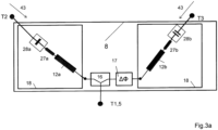
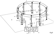
Fig. 1 :
Antenne 1 nach der Erfindung, bestehend im Beispielaus dem Ringleitungsstrahler 2mit dem Ringleiter 14 in der Höhe h < 0,15λ über der leitenden Grundfläche 6 mit N = 3vertikalen Resonanzstrahlern Koppelpunkten und Phasenschiebernetzwerk 8.Die vertikalen Resonanzstrahler Anschlusspunkt 11 mit der leitenden Grundfläche 6 verkoppelt.Die elektromagnetische Erregung 3 erfolgt über das Verteil-und Phasenschiebernetzwerk 8, welches eingangsseitig mit seinem Tor T1mit dem Antennenanschluss 5 verbunden ist und dessen Tore T2 und T3 mit zwei vonden vertikalen Resonanzstrahlern Erregungsstrahler 10a und 10b in der Weise verbunden sind, dass die zugehörigen Ringleitungs-Koppelpunkte den im Verteilnetzwerk 16und im Phasendrehglied 17 bewirkten Ausgangssignalen an den Toren T2 und T3 mit Phasenwinkelunterschied ΔΦ = 360°/N = 120° angesteuert sind, sodass sich aufdem Ringleiter 14 die laufende Leitungswelle einstellt. Hierbei ist erfindungsgemäß vorausgesetzt, dass die Tore T2 und T3 jeweils einen reellen Eingangswiderstand 43 besitzen, sodass die Resonanz desRingleitungsstrahlers 2 durch Anschluss der elektromagnetischen Erregung 3 nicht beeinflusst ist. Zur Impedanzanpassung zwischen dem Verteil-und Phasenschiebernetzwerk 8 an den Toren T2, T3 und der hochohmigen Antennenimpedanz 37 bei der Resonanzfrequenz f0 des Ringleitungsstrahlers 2 (sh.Fig. 2b ) an den Ringleitung-Koppelpunkten 7a und 7b ist das Verteil-und Phasenschiebernetzwerk 8 hochohmig gestaltet und befindet sich auf einem Impedanzniveau von etwa 300 - 500 Ohm. -
Fig. 2 : Figur a)zeigt den Ringleitungsstrahler 2 nach der Erfindung mit drei azimutal gleich verteilten vertikalen Resonanzstrahlern 4a - 4c als Resonanzstruktur.Die Erregung 3 ist nicht dargestellt.Die Blindwiderstandsschaltungen 13 a- 13c sind durch dieKapazitäten Abstimmung des Ringleitungsstrahlers 2 auf eine Resonanzfrequenz- zum Beispiel f0= 1392 MHz - stellt sich anden vertikalen Resonanzstrahlern 4a- 4c jeweils ander mit 42 bezeichneten Messstrecke der inFigur 2b ) dargestellte Verlauf der Antennenimpedanz 37 mit ihrem durch die Strahlung bedingten reellen Resonanzwiderstand von ca. 340 Ohm ein. Bei Anschluss der Erregung andie Resonanzstrahler 4a und 4b - wie inFigur 1 - wird das Resonanzverhalten der Struktur in der Frequenz nicht verändert.Im Beispiel der 3 azimutal gleich verteilten vertikalen Resonanzstrahler 4a, 4b, 4c beträgt der Phasendrehwinkel des Phasendrehglieds ΔΦ= 120°. -
Fig.3 :
Antenne 1 nach der Erfindung wie inFigur 1mit einem Verteilnetzwerk 16 und einem Phasendrehglied 17 auf dem Impedanzniveau Z0 üblicher koaxialer Leitungen (Z0 = 50 Ohm). Zur Anpassung an das hochohmige Impedanzniveau der Antennenimpedanz 37 (sh.Figur 2b ) sinddem Phasendrehglied 17 und einem Arm des Verteilnetzwerks 16jeweils ein Anpassnetzwerk 18 nachgeschaltet.Der Eingangswiderstand 43 an den Toren T2 und T3 ist - ebenso wie inFigur 1 - bei der Resonanzfrequenz desRingleitungsstrahlers 2 hochohmig und reell. -
Fig.3a :
Verteil-und Phasenschiebernetzwerk 8 wie inFigur 3Ringleitungsstrahlers 2 ist durch die λ/4-Transformationsleitungen den Kapazitäten den Induktivitäten 12a und 12b ermöglichen eine Feinkorrektur der Anpassung über einen erweiterten Frequenzbereich. -
Fig.4 :
Antenne nach der Erfindung wie inFigur 3Erregungsstrahlern und Phasenschiebernetzwerks 8. -
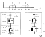
Fig.5 :
Erfindungsgemäße Ausführungsformen der insgesamt kapazitiv wirkenden Blindwiderstandsschaltungen 13 zur Ankopplung der vertikalen Resonanzstrahler andie leitende Grundfläche 6 inFigur 4 - a)
Blindwiderstandsschaltung 13a bzw. 13b der beiden vertikalen aktiven Resonanz-Erregungsstrahler 10a bzw.10b, unterteilt in die ersteBlindwiderstandsschaltung 20a bzw. 20b und dieüber den Verknüpfungspunkt 19a bzw. 19bverbundene zweite Blindwiderstandsschaltung 21a bzw. 21b, jeweils realisiert durch eine erste Kapazität 22a bzw. 22b und entsprechend durch diezweite Kapazität 23a bzw.23b. - b)
Blindwiderstandsschaltung 13c des übrigen passiven vertikalen Resonanzstrahlers 4c, realisiert durch eine Kapazität 28. Die beiden aktiven Resonanz-Erregungsstrahler sind wie in Figur a) beschaltet. - c)
Blindwiderstandsschaltung 13a bzw.13b der beiden vertikalen aktiven Resonanz-Erregungsstrahler 10a bzw.10b wie unter Figur a) jedoch mit einem Parallelresonanzkreis, bestehend aus der Parallelinduktivität 46a bzw. 46b und der Parallelkapazität 23a bzw.23b in der zweiten Blindwiderstandsschaltung 21a bzw. 21b zur Erweiterung der Frequenzbandbreite der Antenne. - d)
Blindwiderstandsschaltung 13c des übrigen passiven vertikalen Resonanzstrahlers 4c, realisiert, wie unter Figur b) jedoch mit einem seriellen Parallelresonanzkreis bestehend aus der Parallelinduktivität 46 und der Parallelkapazität 45 inSerienschaltung zur Kapazität 28 zur Erweiterung der Frequenzbandbreite der Antenne in Entsprechung der Gestaltung der Blindwiderstandsschaltung 13a bzw.13b der beiden vertikalen aktiven Resonanz-Erregungsstrahler 4a bzw. 4b wie unter c). Die beiden aktiven Resonanz-Erregungsstrahler sind wie in Figur c) beschaltet. - e) Darstellung der Frequenzbänder L1 und L2 für die Satelliten-Navigation mit den Mittenfrequenzen fm1 und fm2 und den unteren und oberen Grenzfrequenzen fu1, fo1 bzw.fu2, fo2. Die Frequenz fm beschreibt die Mittenfrequenz zwischen fu1 und fo2.
- f)
Blindwiderstandsschaltung 13a bzw.13b der beiden vertikalen aktiven Resonanz-Erregungsstrahler 10a bzw.10b wie unter Figur c) jedoch mit einem weiteren Parallelresonanzkreis 44a bzw. 44b in Serienschaltung zur ersten Kapazität 22a bzw. 22b hin zum Verknüpfungspunkt 19 zur gesonderten Optimierung der Schaltung für jeweils einen der beiden Frequenzbereiche L1 und L2 zur Gestaltung einer Zweibandantenne. - g)
Blindwiderstandsschaltung 13c des übrigen passiven vertikalen Resonanzstrahlers 4c, realisiert wie unter Figur d), jedoch mit einem weiteren Parallelresonanzkreis 44 inSerienschaltung zur Kapazität 28 inder Blindwiderstandsschaltung 13c. Die beiden aktiven Resonanz-Erregungsstrahler sind wie in Figur f) beschaltet zur Gestaltung einer Zweibandantenne. - h) Blindwiderstandsschaltung 13a bzw.13b der beiden vertikalen aktiven Resonanz-
Erregungsstrahler 10a bzw.10b wie unter Figur f) jedoch mit einer Zusatz-Parallelkapazität 47, gebildet durch die, die isolierte Gegenelektrode 34 überkragende Fläche der Kapazitätselektrode 32a, 32b inden Figuren 13c und13d mit der elektrisch leitenden beschichteten Leiterplatte 35. Die Zusatz-Parallelkapazität 47 ermöglicht die Erweiterung des Bereichs der Impedanzanpassung jeweilsam Verknüpfungspunkt den Ringleitungsstrahler 2. Die Resonanzbedingung und die Impedanzanpassung werden durch Abstimmung der Größen der Kapazitätselektroden 32a, 32b und der isolierten Gegenelektroden 34 aufeinander hergestellt.
- a)
-
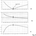
Fig.6 :
Anpassungsverhältnisse bei der Resonanzfrequenz f0 in Abhängigkeit vom Maß "t" für die Unterteilung in die ersteKapazität Figur 4 .- a) Reflexionsfaktor an
der Antennenanschlusstelle 5 als Eingangstor T1 eines verlustfreien Verteil-und Phasenschiebernetzwerks 8der Antenne 1 in Abhängigkeit vom Teilungsmaß t . Anpassung ist mit topt = 0,13 erreicht. - b) Transformationsfaktor bei der Resonanzfrequenz f0
zwischen dem Eingangswiderstand 43 mit Z0 = 50 Ohm desPhasendrehglieds 17 und dem Resonanzwiderstand bei f0 am Ringleitungsstrahler-Koppelpunkt 7 in Abhängigkeit vom Teilungsmaß t. - c) Relative Leistung P/Pmax bei f0 in Abhängigkeit vom Teilungsmaß t.
- a) Reflexionsfaktor an
-
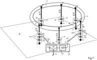
Fig.7 :
Antenne nach der Erfindung mit Widerstands-Anpassung durch kapazitive Unterteilung wie im Beispiel derFigur 4 jedochmit insgesamt 6 azimutal um jeweils 60° gegeneinander versetzt verteilten vertikalen Resonanzstrahlern 4a .. 4f, von denen vier als vertikalepassive Resonanzstrahler 9a..9d gestaltet sind.Die Erregung 3 erfolgt beispielhaft an den beiden um 120° azimutal gegeneinander versetzten und um den Differenzwinkel ΔΦ= 120° erregten vertikalen Resonanz-Erregungsstrahlern -
Fig.8 :
Antenne nach der Erfindung wie inFigur 7jedoch mit insgesamt 8 azimutal um jeweils 45° gegeneinander versetzt verteilten vertikalen Resonanzstrahlern 4a..4h.Die Erregung 3 erfolgt beispielhaft an den beiden um 90° azimutal gegeneinander versetzten und um den Differenzwinkel ΔΦ= 90° erregten vertikalen Resonanz-Erregungsstrahlern -
Fig.9 :
Antenne nach der Erfindung mit rechteckig ausgeführter Ringleitung 14 mit vier vertikalen Resonanzstrahler4a bis 4d im Bereich der Ringleitungs-Ecken. Zwei der vertikalen Resonanzstrahler sind als vertikale Resonanz-Erregungsstrahler und Phasenschiebernetzwerk 8 ist durch kapazitive Unterteilung, ähnlich wie inden Figuren 4 ,7 und8 erreicht.Die Ringleitung 14 ist vorzugsweise quadratisch gestaltet mit gleichen Ringleiterbreiten 15a, 15b und gleichen Ringleitungs-Abschnitten Sowohl die Ringleiterbreite Abschnitte -
Fig. 10 :Rechteckförmiger Ringleitungsstrahler 2 einerAntenne 1 nach der Erfindung ohne Darstellung der elektromagnetischen Erregung 3 zur Erläuterung der Resonanzstruktur desRingleitungsstrahlers 2.- a) geometrischer Aufbau des
Ringleitungsstrahlers 2 mit großen unterschiedlich wählbaren Ringleiterbreiten 15a und 15b sowie den unterschiedlich wählbaren Ringleitungs-Abschnitten 30a und 30b.Die vertikalen Resonanzstrahler 4a - 4d sind mit ihren Ringleitungs-Koppelpunkten 7a - 7d im weiten Bereich der Ecken des rechteckförmigen Ringleiters 14 vorgesehen. Die unterbrochene Linie kennzeichnet etwa denVerlauf der Schwerlinie 24 der Stromdichteverteilung der Leitungswelle bei Erregung desRingleitungsstrahlers 2. Aufgrund der Stromverdrängung verdichtet sich die Stromverteilung hin zum Rand desRingleiters 14. Der für die Funktion bei der Erregung desRingleitungsstrahlers 2 relevante Strom der Leitungswelle fließt demnach - gekennzeichnet durch die als unterbrochene Linie gezeichnete Schwerlinie der Stromverteilung 24 - auch bei großen Leiterbreiten 15a, 15b mehr zum Rand hin gedrängt. Dies gilt insbesondere für sehr große Ringleiterbreiten 15a, 15b bis hin zur vollkommenen Schließung der inneren Öffnung zum Zentrum hin, welches praktisch stromlos ist, wenn die Ringleitung 14 als eine geschlossene leitende Fläche realisiert ist. - b) gemäß dem durch die Schwerpunktlinie der Stromdichteverteilung 24 repräsentierten Strom kann die Resonanzstruktur des
Ringleitungsstrahlers 2 durch ein grob angenähertes Ersatzschaltbild allgemein wiedergegeben werden. Die einzelnen Ringleitungs-Abschnitte 30a -30d sind jeweils durch die induktive und kapazitive Wirkung des zugehörigen Abschnitts der Ringleitung 14 unter Einbeziehung der kapazitiven Wirkung der Blindwiderstandsschaltung 13 als konzentrierte induktive Elemente (Ln) und kapazitive Elemente (Cn) dargestellt. Jeder n-te Ringleitungsabschnitt 30a - 30b ist durch eine π-Struktur gemäß Figur c), bestehend aus einer Längsinduktivität 2*Ln und jeweils einer Querkapazität Cn an deren beiden Enden, dargestellt. Die Strahlungsdämpfung jedeshorizontal orientierten Ringleitungsabschnitt 30a - 30b ist durch den Dämpfungsfaktor d der konzentrierten Induktivität einbezogen. Die Aneinanderreihung einander benachbarter Ringleitungs-Abschnitte 30a-30d erfolgt jeweils über einen gemeinsamen vertikalen Resonanzstrahler 4a..4d unter Zusammenziehung der Querkapazitäten Cn der benachbarten Ringleitungs-Abschnitte, wie in Figur c) dargestellt. Die geringfügige induktive Wirkung der vertikalen Resonanzstrahler ist bei dieser Grundsatzbetrachtung aufgrund der geringen Antennenhöhe h vernachlässigt. Erfindungsgemäß vorteilhafte Voraussetzungen fürden Ringleitungsstrahler 2 sind für die Resonanzfrequenz f0=ωo/2π dann erreicht, wenn jeweils alle Wellenwiderstände

- a) geometrischer Aufbau des
Bei rotationssymmetrischen Ringleitungsstrahlern 2 ist dies stets gegeben. Andernfalls kann diese Voraussetzung zum Beispiel bei einer rechteckförmigen Struktur desRingleitungsstrahlers 2 durch individuelle Gestaltung derRingleiterbreiten 15a-15d in den einzelnen Ringleitungs-Abschnitten 30a-30b erreicht werden.
-
Fig.11 :- a) Gestaltung des Verteil- und Phasenschiebernetzwerks 8 - zum Beispiel wie in
den Figuren 7 und8 - jedoch als auf die Resonanzfrequenzf0 abgestimmten Hybridring 3, durch welchen sowohl die Leistungsteilung als auch die Phasenverschiebung erfolgt. Bei Einspeisung am Tor T1 wird der Ringleitungsstrahler 2 über die Tore T2 und T3 mitdem Phasenunterschied von 90° erregt. Der Abschluss von Tor T4 mitdem ohmschen Abschlusswiderstand 40 bewirkt bei Abweichung der Frequenz von der Resonanzfrequenz f0 breitbandig die teilweise Absorption der Leistung der unerwünschten Polarisation bei Einspeisung am Tor T1. - b) Idealisierte Streumatrix zur Beschreibung des allgemein bekannten grundsätzlichen Wellenverhaltens eines Hybridrings 38 in Figur a) an den Toren T1 bis T4. Die wichtige Entkopplung der Tore T1 und T4 voneinander ist durch die Streuparameter S14 = 0, S41 = 0 in der Matrix fett gekennzeichnet.
- c) Gestaltung des Verteil- und Phasenschiebernetzwerks 8 - zum Beispiel wie in
den Figuren 7 und8 - jedoch als auf die Resonanzfrequenz f0 abgestimmten Wilkinson-Teilers 16 mit nachgeschaltetem λ/4 Leitungs-Phasenschieber 17 an einem Tor T3* zur Erzeugung desPhasenunterschieds von 90°. Der ohmsche Symmetrierungswiderstand 40 absorbiert bei unsymmetrischer Belastung des Wilkinson-Teilers 16 bei Abweichung von der Resonanzfrequenz f0 teilweise die Ströme, welche die unerwünschte Polarisation aufdem Ringleitungsstrahler 2 hervorrufen.
- a) Gestaltung des Verteil- und Phasenschiebernetzwerks 8 - zum Beispiel wie in
-
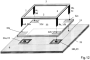
Fig.12 :
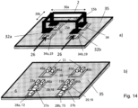
Antenne nach der Erfindung z. B. wie inFigur 9 mit rechteckig geformter Ringleitung 14.Die Kapazitäten Platte 33 sind dieKapazitäten 28 zur Ankopplung der passiven vertikalen Resonanzstrahler 4c, 4d an die elektrisch leitende Grundfläche 6 gestaltet. Zur kapazitiven Ankopplung der aktiven vertikalen Resonanzstrahler 10a, 10b an die Tore T2 und T3 des Verteil-und Phasenschiebernetzwerks 8 ist dieser Anschluss als jeweils eine von der leitenden Schicht isolierte, flächige Gegenelektrode 34 gestaltet.Die Gegenelektroden 34 könnensomit als Verknüpfungspunkte 19 der Antenne inFigur 9 ausgeführt sein und können als Anschlusspunkte für die Tore T2 und T3 des Verteil-und Phasenschiebernetzwerks 8, wie inFigur 13 -
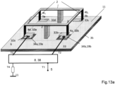
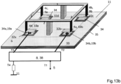
Fig.13 :
Antenne 1 ähnlich wie inFigur 11Platte 33 durch einen Luftspalt realisiert. TypischeAbmessungen eines Ringleitungsstrahlers 2 für den Frequenzbereich L1 sind für quadratische Antennen ein Abmessung von 30mm bis 40mm und für die Höhe h = 8mm. Zur Widerstandsanpassung des vorzugsweise auf niedrigem Impedanzniveau (Z0) ausgeführten Verteil-und Phasenschiebernetzwerks 8 ist die kapazitive Unterteilung wie inFigur 9 vorgesehen.- a) Die beispielhaft zugehörigen Blindwiderstandsschaltungen 13a, 13b und 13c sind in den
Figuren 5a und 5b dargestellt.Die Kapazität 28der Kapazitätselektrode Kapazität und Phasenschiebernetzwerks 8 mit ihrem reellen Eingangswiderstand 43 sind jeweils aneine Gegenelektrode 34b als Verknüpfungspunkt Kapazität dem Verknüpfungspunkt und dem Massepunkt 11 eingebrachte Kapazität mit der Gegenelektrode 34 einerseits und andererseits z.B. über dieKapazität Fig. 4 u. 5a) mit Masse verbunden sind. - b) die
Blindwiderstandsschaltungen Erregungsstrahler Figur 5a bzw. wie in 5c gestaltet. Bei Gestaltung nachFigur 5c ist der auf der Rückseite der beschichteten Leiterplatte 35 eingebrachten Kapazität 23a,23b eine Induktivität 9b den Kapazitätselektroden isolierte Gegenelektroden 34 gegenübergestellt. Ausgehendvon der Gegenelektrode 34 als Kontaktstützpunkt sind auf der Rückseite der Leiterplatte 35 die Parallelinduktivität 46 und dieParallelkapazität 45zum Massepunkt 11 auf der Leiterplatte 35 geschaltet, sodass dieBlindwiderstandsschaltung 13 inFigur 5d realisiert ist.
BeiAusgestaltung aller Blindwiderstandsschaltungen 13 aller vertikalen Resonanzstrahler mit jeweils einer Kapazitätselektrode 32 und einer gegenüberliegenden isolierten Gegenelektrode 34 können alle Schaltungen in denFiguren 5c und5f für die Resonanz-Erregungsstrahler Figuren 5d und5g angegebenen Schaltungen realisiert werden. - c) Wie unter
Figur 5h beschrieben dient die Zusatz-Parallelkapazität 47 zur freien Gestaltung der Impedanzanpassung bei Beibehaltung der Resonanzeigenschaften desRingleitungsstrahlers 2. Die Figur zeigt die großflächige Überdeckung der isolierten Gegenelektrode 34a, 34bmit der Kapazitätselektrode Erregungsstrahler Parallelkapazität 47. Die Blindwiderstandsschaltung der beiden passiven Resonanzstrahler 9a, 9b sind wie in Figur a) gestaltet. - d) die
Blindwiderstandsschaltungen 13 der beiden Resonanz-Erregungsstrahler Parallelkapazität 47 gestaltet. Die beispielhaft möglichen Blindwiderstandsschaltungen 13 der beiden passiven Resonanzstrahler 9a, 9b können wie in Figur b) beschrieben, gestaltet werden.
- a) Die beispielhaft zugehörigen Blindwiderstandsschaltungen 13a, 13b und 13c sind in den
-
Fig.14 :
Im Bild ist dieOberseite der Leiterplatte 35 einerAntenne 1 nach der Erfindung dargestellt, auf welche der elektrische Ringleitungsstrahler 2 aufgesetzt wird. Für die breitbandige Gestaltung einerAntenne 1 nach der Erfindung - welche zum Beispiel beide Frequenzbereiche L1 und L2 mit einer zwischen den beiden Frequenzbereichen liegenden Mittenfrequenz fm (sh.Figur 5e ) -ist die Blindwiderstandsschaltung 13, wie in denFiguren 5c bzw. 5d gestaltet. Hierfür ist für die Blindwiderstandsschaltung in den beiden aktiven vertikalen Resonanz-Erregungsstrahlern Blindwiderstandsschaltung Figur 5c und für die beiden passiven vertikalen Resonanzstrahler 9a, 9b dieBlindwiderstandsschaltung 13c inFigur 5d vorgesehen. Dies ist bei demBeispiel im Figur 13a dadurch erreicht, dass für alle Kapazitätselektroden 32 jeweils eine Gegenelektrode 34 vorhanden ist und, dass der durch die Kapazitätselektroden 32 bewirkten Kapazität 22a, 22b bzw. 28 anallen vertikalen Resonanzstrahlern 4a - 4d eine Parallelschaltung aus einer Parallelkapazität 23a, 23b bzw. 45 und einer Parallelinduktivität 46a, 46b, bzw. 46 - dargestellt als SMD- Bauteile - zwischen der Gegenelektrode 34 und der elektrisch leitenden Grundfläche 6 in Serie geschaltet ist.Figur 13aOberseite der Leiterplatte 35mit Durchkontaktierungen 26 aufden Gegenelektroden 34 unter den Kapazitätselektroden 32. InFigur 14b ist dieUnterseite der Leiterplatte 35 mit den Pads 29 dargestellt, welche mitden isolierten Gegenelektroden 34 über dieDurchkontaktierungen 26 verbunden sind,. Die Blindelemente sind als SMD-Bauelemente gemäß denFiguren 5c und 5d angebracht. Zusätzlich sind die beiden Verknüpfungspunkte 19 mit der jeweils daran angeschlossenen Serienschaltung aus der Kapazität 28a, 28b und der Induktivität 27a, 27b als Teile der inFigur 3a enthaltenenAnpassungsschaltung 18 des Verteil-und Phasenschiebernetzwerks 8 zur Bildung der Tore T2 und T3 dargestellt. -
Fig. 15
Zeigt eine Antenne nach der Erfindung mit vier azimutal amUmfang der Ringleitung 14 gleich verteilten Resonanz-Erregungsstrahlern 10a bisErregerstrahler Erregerstrahler Erregungsstrahler und Phasenschiebernetzwerks und Phasenschiebernetzwerks 8, 38b verbunden ist. Auch hier kommt erfindungsgemäß vorzugsweise jeweils ein Hybridring 38 zum Einsatz. Das 180° Phasennetzwerk 31 kann beispielhaft als Wilkinson-Teiler 39 mit einer λ/2-langen Verzögerungsleitung 17 (sh.Figur 11c ) eingesetzt werden. Alle Anschlüsse sind in der Weise gewählt, dass sich auf der Ringleitung die leitende Welle in der gewünschten Umlaufrichtung einstellt. Mit dieser Anordnung ist der besondere Vorteil der azimutal symmetrischen Anregung verbunden, sodass der Abgleich der Anordnung besonders problemfrei erfolgen kann. Als Einschränkung ist jedoch der erhöhte Aufwand anzumerken.
-
Fig.1 :
Antenna 1 according to the invention, consisting in the example of thering line radiator 2 with thering conductor 14 at the height h < 0.15λ above theconductive base surface 6 with N = 3vertical resonance radiators line coupling points electromagnetic excitation 3 through the distribution andphase shifter network 8. Thevertical resonance radiators conductive base surface 6 via acapacitive reactance circuit ground connection point 11. Theelectromagnetic excitation 3 is carried out via the distribution andphase shifter network 8, which is connected on the input side with its gate T1 to theantenna connection 5 and whose gates T2 and T3 are connected to two of thevertical resonance radiators resonance excitation radiators line coupling points distribution network 16 and in thephase shifter 17 at the gates T2 and T3 with a phase angle difference ΔΦ = 360°/N = 120°, so that the current line wave is set on thering conductor 14. In this case, it is assumed according to the invention that the gates T2 and T3 each have areal input resistance 43, so that the resonance of thering line radiator 2 is not influenced by the connection of theelectromagnetic excitation 3. For impedance matching between the Distribution andphase shifting network 8 at the gates T2, T3 and the high-resistance antenna impedance 37 at the resonance frequency f0 of the ring line radiator 2 (seeFig. 2b ) at the ringline coupling points phase shifting network 8 is designed to be high-impedance and is at an impedance level of approximately 300 - 500 ohms. -
Fig.2 : Figure a) shows thering line radiator 2 according to the invention with three azimuthally equally distributedvertical resonance radiators 4a - 4c as a resonance structure. Theexcitation 3 is not shown. Thereactance circuits 13 a - 13 c are realized by thecapacitors ring line radiator 2 is tuned to a resonance frequency - for example f0 = 1392 MHz - thevertical resonance radiators 4a - 4c each have the measurement section designated 42.Figure 2b ) with its real resonance resistance of about 340 Ohms caused by the radiation. When the excitation is connected to theresonance radiators Figure 1 - the resonance behavior of the structure is not changed in frequency. In the example of the three azimuthally equally distributedvertical resonance radiators -
Fig.3 :
Antenna 1 according to the invention as inFigure 1 but with adistribution network 16 and aphase shifter 17 at the impedance level Z0 of usual coaxial lines (Z0 = 50 Ohm). To adapt to the high-impedance level of the antenna impedance 37 (seeFigure 2b ), thephase shifter 17 and an arm of thedistribution network 16 are each followed by amatching network 18. Theinput resistance 43 at the gates T2 and T3 is - as inFigure 1 - at the resonance frequency of thering line radiator 2, high-impedance and real. -
Fig.3a :
Distribution andphase shifting network 8 as inFigure 3 with exemplary design of thematching networks 18 at the two outputs. The matching at resonance of thering line radiator 2 is effected by the λ/4transformation lines antenna impedance 37 is provided. The series resonance circuits, consisting of thecapacitances inductances -
Fig.4 :
Antenna according to the invention as inFigure 3 but with a special design of thereactance circuits resonance excitation radiators first reactance circuit second reactance circuit connection point phase shifter network 8. -
Fig.5 :
Inventive embodiments of the overallcapacitive reactance circuits 13 for coupling the vertical resonance radiators to theconductive base surface 6 inFigure 4 - a)
Reactance circuit resonance excitation radiators first reactance circuit second reactance circuit connection point first capacitance second capacitance - b)
Reactance circuit 13c of the remaining passivevertical resonance radiator 4c, realized by acapacitor 28. The two active resonance excitation radiators are connected as in Figure a). - c)
Reactance circuit resonance excitation radiators parallel inductance parallel capacitance second reactance circuit - d)
Reactance circuit 13c of the remaining passivevertical resonance radiator 4c, implemented as in Figure b), but with a serial parallel resonance circuit consisting of theparallel inductance 46 and theparallel capacitance 45 in series with thecapacitance 28 to extend the frequency bandwidth of the antenna in accordance with the design of thereactance circuit resonance excitation radiators - e) Representation of the frequency bands L1 and L2 for satellite navigation with the center frequencies fm1 and fm2 and the lower and upper limit frequencies fu1, fo1 and fu2, fo2 respectively. The frequency fm describes the center frequency between fu1 and fo2.
- f)
Reactance circuit resonance excitation radiators parallel resonance circuit first capacitor connection point 19 for separate optimization of the circuit for each of the two frequency ranges L1 and L2 to design a two-band antenna. - g)
Reactance circuit 13c of the remaining passivevertical resonance radiator 4c, implemented as in Figure d), but with a furtherparallel resonance circuit 44 in series with thecapacitance 28 in thereactance circuit 13c. The two active resonance excitation radiators are connected as in Figure f) to form a two-band antenna. - h)
Reactance circuit resonance excitation radiators parallel capacitance 47, formed by the surface of thecapacitance electrode insulated counter electrode 34 in theFigures 13c and13d with the electrically conductivecoated circuit board 35. The additionalparallel capacitance 47 enables the range of the impedance matching to be extended at theconnection point ring line radiator 2. The resonance condition and the impedance matching are established by matching the sizes of thecapacitance electrodes insulated counter electrodes 34 to one another.
- a)
-
Fig.6 :
Adaptation ratios at the resonance frequency f0 depending on the dimension "t" for the division into thefirst capacity second capacity ring line radiator 2 inFigure 4 .- a) Reflection factor at the
antenna connection point 5 as input port T1 of a loss-free distribution andphase shift network 8 of theantenna 1 as a function of the pitch t . Adaptation is achieved with topt = 0.13. - b) Transformation factor at the resonance frequency f0 between the
input resistance 43 with Z0 = 50 Ohm of thephase shifter 17 and the resonance resistance at f0 at the ring lineradiator coupling point 7 as a function of the pitch t. - c) Relative power P/Pmax at f0 depending on the pitch t.
- a) Reflection factor at the
-
Fig.7 :
Antenna according to the invention with resistance matching by capacitive subdivision as in the example ofFigure 4 but with a total of 6vertical resonance radiators 4a .. 4f, each azimuthally offset by 60°, of which four are designed as verticalpassive resonance radiators 9a..9d. Theexcitation 3 takes place, for example, at the two azimuthally offset by 120° verticalresonance excitation radiators -
Fig.8 :
Antenna according to the invention as inFigure 7 , but with a total of 8vertical resonance radiators 4a..4h, each azimuthally offset by 45° from each other. Theexcitation 3 takes place, for example, at the two verticalresonance excitation radiators -
Fig.9 :
Antenna according to the invention withrectangular ring line 14 with fourvertical resonance radiators 4a to 4d in the area of the ring line corners. Two of the vertical resonance radiators are designed as verticalresonance excitation radiators vertical resonance radiators phase shift network 8 is achieved by capacitive subdivision, similar to theFigures 4 ,7 and8th Thering line 14 is preferably designed to be square with the samering line widths ring line sections ring line width ring line sections -
Fig.10 :- Rectangular
ring line radiator 2 of anantenna 1 according to the invention without representation of theelectromagnetic excitation 3 to explain the resonance structure of thering line radiator 2.- a) geometric structure of the
ring line radiator 2 with large, differently selectablering line widths ring line sections vertical resonance radiators 4a - 4d are with their ringline coupling points 7a - 7d in the wide area of the corners of therectangular ring line 14 provided. The broken line roughly indicates the course of thecenter line 24 of the current density distribution of the line wave when thering line radiator 2 is excited. Due to the current displacement, the current distribution is concentrated towards the edge of thering conductor 14. The current of the line wave relevant for the function when thering line radiator 2 is excited therefore flows - indicated by the center line of thecurrent distribution 24 drawn as a broken line - more towards the edge even withlarge conductor widths ring conductor widths ring line 14 is implemented as a closed conductive surface. - b) according to the current represented by the center of gravity of the
current density distribution 24, the resonance structure of thering line radiator 2 can be generally represented by a roughly approximated equivalent circuit diagram. The individualring line sections 30a - 30d are each represented by the inductive and capacitive effect of the associated section of thering line 14, including the capacitive effect of thereactance circuit 13, as concentrated inductive elements (Ln) and capacitive elements (Cn). Each n-thring line section 30a - 30b is represented by a π structure according to figure c), consisting of alongitudinal inductance 2*Ln and a transverse capacitance Cn at both ends. The radiation attenuation of each horizontally orientedring line section 30a - 30b is included by the attenuation factor d of the concentrated inductance. The connection of adjacentring line sections 30a-30d is carried out via a commonvertical resonance radiator 4a..4d by contracting the transverse capacitances Cn of the adjacent ring line sections, as shown in Figure c). The slight inductive effect of the vertical resonance radiator is neglected in this basic consideration due to the low antenna height h. Advantageous conditions according to the invention for thering line radiator 2 are achieved for the resonance frequency f0=ωo/2π when all wave impedances
- a) geometric structure of the
- This is always the case with rotationally symmetrical
ring line radiators 2. Otherwise, this requirement can be met, for example with a rectangular structure of thering line radiator 2, by individually designing thering line widths 15a-15d in the individualring line sections 30a-30b.
- Rectangular
-
Fig.11 :- a) Design of the distribution and phase shifting network 8 - for example as in the
Figures 7 and8th - but as ahybrid ring 3 tuned to the resonance frequency f0, through which both the power division and the phase shift occur. When fed in at gate T1, thering line radiator 2 is excited via gates T2 and T3 with a phase difference of 90°. The termination of gate T4 with theohmic termination resistor 40 causes the partial absorption of the power of the undesired polarization over a broadband band when fed in at gate T1 if the frequency deviates from the resonance frequency f0. - b) Idealized scattering matrix to describe the generally known fundamental wave behavior of a hybrid ring 38 in Figure a) at the gates T1 to T4. The important decoupling of the gates T1 and T4 from each other is marked in bold in the matrix by the scattering parameters S14 = 0, S41 = 0.
- c) Design of the distribution and phase shifting network 8 - for example as in the
Figures 7 and8th - but as aWilkinson divider 16 tuned to the resonance frequency f0 with a downstream λ/4line phase shifter 17 at a gate T3* to generate the phase difference of 90°. Theohmic balancing resistor 40 partially absorbs the currents that cause the undesired polarization on thering line radiator 2 when theWilkinson divider 16 is loaded asymmetrically and deviates from the resonance frequency f0.
- a) Design of the distribution and phase shifting network 8 - for example as in the
-
Fig.12 :
Antenna according to the invention, for example as inFigure 9 with rectangular shapedring line 14. Thecapacities vertical Resonance radiators 4a - 4d are formed at their lower end into individually designedflat capacitance electrodes conductive base surface 6, which is designed as an electrically conductively coated circuit board, thecapacitances 28 are designed to couple the passivevertical resonance radiators conductive base surface 6. For the capacitive coupling of the activevertical resonance radiators phase shift network 8, this connection is designed as aflat counter electrode 34 insulated from the conductive layer. Thecounter electrodes 34 can thus be used as connection points 19 of the antenna inFigure 9 and can be used as connection points for the gates T2 and T3 of the distribution andphase shifting network 8, as shown inFigure 13 indicated, serve. -
Fig.13 :
Antenna 1 similar toFigure 11 , however, the dielectric effect of thedielectric plate 33 is realized by an air gap. Typical dimensions of aring line radiator 2 for the frequency range L1 are a dimension of 30mm to 40mm for square antennas and a height of h = 8mm. To adjust the resistance of the distribution andphase shift network 8, which is preferably designed at a low impedance level (Z0), the capacitive subdivision is as inFigure 9 intended.- a) The
exemplary reactance circuits Figures 5a and 5b Thecapacitance 28 of thecapacitance electrode conductive base surface 6 and thecapacitance insulated counter electrode phase shift network 8 with theirreal input resistance 43 are each connected to acounter electrode connection point capacitance capacitance capacitance connection point ground point 11 is attached to the back of thecoated circuit board 35 as an SMD component. For this purpose, insulated pads 29 are designed as contact points on the back of the circuit board, each of which is connected to theCounter electrode 34 on the one hand and on the other hand e.g. via thecapacitance Fig.4 and 5a) are connected to ground. - b) the
reactance circuits resonance excitation radiators Figure 5a or as in 5c. When designed according toFigure 5c aninductance capacitance coated circuit board 35. In contrast to Figure a),insulated counter electrodes 34 are placed opposite thecapacitance electrodes coated circuit board 35 to form the reactance circuits of the twopassive resonance radiators counter electrode 34 as a contact support point, theparallel inductance 46 and theparallel capacitance 45 are connected to theground point 11 on thecircuit board 35 on the back of thecircuit board 35, so that thereactance circuit 13 inFigure 5d is realized.
When designing allreactance circuits 13 of all vertical resonance radiators with a capacitance electrode 32 and an oppositeinsulated counter electrode 34, all circuits can beFigures 5c and5f for theresonance excitation radiators circuit board 35. In the same way, the reactance circuits for thepassive resonance radiators insulated counter electrodes 34 with SMD components on the back of thecircuit board 35 according to theFigures 5d and5g specified circuits can be realized. - c) As under
Figure 5h As described above, the additionalparallel capacitance 47 serves to freely design the impedance matching while maintaining the resonance properties of thering line radiator 2. The figure shows the large-area overlap of theinsulated counter electrode capacitance electrode resonance excitation radiators capacitance electrode insulated counter electrode 34 forms the additionalparallel capacitance 47 with the electrically conductive layer of thecoated circuit board 35. The Reactance circuit of the twopassive resonance radiators - d) the
reactance circuits 13 of the tworesonance excitation radiators parallel capacitance 47. Theexemplary reactance circuits 13 of the twopassive resonance radiators
- a) The
-
Fig.14 :
The picture shows the top side of thecircuit board 35 of anantenna 1 according to the invention, onto which the electricalring line radiator 2 is placed. For the broadband design of anantenna 1 according to the invention - which, for example, has both frequency ranges L1 and L2 with a center frequency fm lying between the two frequency ranges (seeFigure 5e ) - is thereactance circuit 13, as shown in theFigures 5c or 5d. For this purpose, thereactance circuit resonance excitation radiators Figure 5c and for the two passivevertical resonance radiators reactance circuit 13c inFigure 5d This is the case in the example inFigure 13a This is achieved by providing acounter electrode 34 for each capacitance electrode 32 and by connecting a parallel circuit comprising aparallel capacitance parallel inductance counter electrode 34 and the electricallyconductive base surface 6 to thecapacitance vertical resonance radiators 4a - 4d.Figure 13a shows the top side of thecircuit board 35 withvias 26 on thecounter electrodes 34 under the capacitance electrodes 32. InFigure 14b the underside of thecircuit board 35 is shown with the pads 29, which are connected to theinsulated counter electrodes 34 via the through-holes 26. The dummy elements are SMD components according to theFigures 5c and 5d In addition, the twoconnection points 19 with the series circuit connected to them, consisting of thecapacitance inductance Figure 3a includedadaptation circuit 18 of the distribution andphase shift network 8 for forming the gates T2 and T3. -
Fig. 15
Shows an antenna according to the invention with fourresonance excitation radiators 10a to 10d distributed azimuthally on the circumference of thering line 14. All radiators are excited according to a rotating wave with a 90° phase difference between adjacent radiators. For this purpose, a first and a second distribution and phase shifter network (8) with a phase angle ΔΦ = 90° are present, the first distribution and phase shifter network (8) being coupled with its gates T2, T3 to a first pair ofresonance excitation radiators excitation radiators resonance excitation radiators phase shifter network phase shifter network 8, 38b. Here too, according to the invention, a hybrid ring 38 is preferably used. The 180° phase network 31 can, for example, be designed as a Wilkinson divider 39 with a λ/2-long delay line 17 (seeFigure 11c ). All connections are selected in such a way that the conductive wave on the ring line is aligned in the desired direction of rotation. This arrangement has the particular advantage of azimuthally symmetrical excitation, so that the adjustment of the arrangement can be carried out particularly easily. One limitation, however, is the increased effort.
Für die Gestaltung einer zweibandfähigen Multibandantenne nach der Erfindung - zum Beispiel für die Frequenzbereiche L1 und L2 - ist die Blindwiderstandsschaltung 13 jeweils in der Weise mehrfrequent gestaltet, dass Resonanz des Ringleitungsstrahlers 2 in den voneinander getrennten Frequenzbändern L1 und L2 jeweils gesondert und entsprechend als Frequenz f01 und als Frequenz f02 gegeben ist. Hierzu wird ausgehend von den Pads 29 in
Im Folgenden wird die Erfindung noch einmal im Zusammenhang mit ihren vorteilhaften Ausführungsformen beschrieben.The invention is described again below in connection with its advantageous embodiments.
In einer Grundform enthält eine Antenne 1 nach der Erfindung einen bereits oben beschriebenen Ringleitungsstrahler 2, wie er zum Beispiel in
Erfindungsgemäß ist diese Resonanzstruktur bei der Eigenresonanzfrequenz f0 befähigt, bei entsprechender Erregung über zwei vertikale Resonanzstrahler 4a, 4b - hier zur Kennzeichnung als vertikale Resonanz-Erregungsstrahler 10a, 10b bezeichnet - mit in der Phase der azimutalen Position der vertikalen Resonanzstrahler 4a, 4b entsprechenden Signalen - zum Beispiel wie in
Naturgemäß kann die Bedingung für die Erregung einer Laufrichtung exakt nur bei der Resonanzfrequenz f0 erfüllt sein und der Anteil der unerwünschten Laufrichtung und somit die Kreuzpolarisation nehmen mit wachsender Abweichung von dieser Frequenz zu. Als besonderer Vorteil der Erfindung ergibt sich jedoch die sehr große Bandbreite für eine hinreichend große Unterdrückung der Kreuzpolarisation aus der erfindungsgemäßen Forderung nach einem reellen Eingangswiderstand 43 beider Tore T2, T3 des Verteil- und Phasenschiebernetzwerks 8, wobei die Resonanzfrequenz f0 des Ringleitungs-strahlers 2 durch die Erregung 3 bei der Resonanzfrequenz f0 nicht geändert wird. Ein Blindleistungsaustausch zwischen dem Ringleitungsstrahler 2 und der Erregung 3 findet somit bei der Resonanzfrequenz f0 nicht statt. Besonders hohe Bandbreite der Unterdrückung der Kreuzpolarisation wird erreicht, wenn - wie in
Erfindungsgemäß ist also vorgesehen, den Ringleitungsstrahler 2 und die Phasenverschiebung um den Winkel ΔΦ im Verteil- und Phasenschiebernetzwerk 8 in der Weise aufeinander abzustimmen, dass dieser Winkel bei der Resonanzfrequenz f0 der elektrischen Länge des Ringleitungs-Abschnitts 30 als Winkelmaß dem Anteil aus der elektrischen Länge 2π der Ringleitung 14 zwischen den beiden vertikalen Resonanz-Erregungsstrahlern 10a, 10b entspricht, an welche die Tore T2 und T3 angeschlossen sind. Dabei können zwischen den vertikalen Resonanz-Erregungsstrahlern 9a, 9b am Ringleiter 14 weitere, jedoch passive vertikale Resonanzstrahler 4 - wie in den
Hierbei ergibt sich für insgesamt N > 3 vertikale Resonanzstrahler 4a, 4b, 4c, 4d und somit die gleiche Anzahl von Ringleitungs-Abschnitten 30a, 30b, 30c, 30d und über die Ringleitung 14 gleich verteilte Koppelpunkte 7 der erfindungsgemäß eingestellte Phasenwinkel des Verteil- und Phasenschiebernetzwerks 8 zu ΔΦ = n*2π/N < 180°, wenn zwischen den Koppelpunkten 7 der beiden vertikalen Resonanz-Erregungsstrahler 10a, 10b n Ringleitungs-Abschnitte 30 gewählt sind.This results in a total of N>3
Für rotationsymmetrische Anordnungen mit hoher Anzahl von insgesamt N Ringleitungs-Abschnitten kann vorteilhaft eine große Frequenzbandbreite für die Unterdrückung der Kreuzpolarisation erreicht werden.For rotationally symmetrical arrangements with a large number of N ring line sections in total, a large frequency bandwidth for suppressing cross polarization can advantageously be achieved.
Für besondere Anwendungen, wie zum Beispiel für die Überlagerung von zirkular polarisierter Strahlung mit azimutaler Phasenverteilung von 2π und einer zirkular polarisierten Strahlung mit azimutaler Phasenverteilung von 4π in einem Antennendiversity-System mit zwei Antennen kann die Erfindung in vorteilhafter Weise ebenso auf einen Ringleitungsstrahler 2 mit einer elektrischen Länge von 4π wie folgt angewandt werden. In einem einfachen Sonderfall mit einem polygonförmigen Ringleitungsstrahler 2 mit über die elektrische Länge 4π azimutal gleich verteilten N = 8 Ringleitungs-Abschnitten 30 werden zwei zueinander benachbarte vertikale Resonanz-Erregungsstrahler 10a, 10b (n = 1) über ein Verteil- und Phasenschiebernetzwerk 8 mit ΔΦ = π/2 erregt. In Analogie hierzu ist mit N = 16 vertikalen Resonanzstrahlern und n = 2 Ringleitungs-Abschnitten zwischen den beiden vertikalen Resonanz-Erregungsstrahlern 10a, 10b demnach der Phasenwinkel ΔΦ = n*4π/N ebenfalls ΔΦ = π/2 einzustellen. Auf zweckmäßige und raumsparende Weise können zwei Ringleitungsstrahler 2 mit unterschiedlicher Phasenverteilung konzentrisch zueinander angeordnet sein in der Weise, dass der Strahler mit azimutaler 2π- Phasenverteilung von dem Strahler mit 4π-Phasenverteilung umringt ist.For special applications, such as for the superposition of circularly polarized radiation with an azimuthal phase distribution of 2π and a circularly polarized radiation with an azimuthal phase distribution of 4π in an antenna diversity system with two antennas, the invention can also advantageously be applied to a
In vorteilhafter Weise erfolgt die Erregung der Ringleitung 14 mit der elektrischen Länge 2π des auf die Resonanzfrequenz f0 abgestimmten Ringleitungsstrahlers 2 in
In einer vorteilhaften Ausgestaltung der Erfindung sind in
In einer vorteilhaften Ausgestaltung der Erfindung erfolgt die Impedanzanpassung zwischen den niederohmig - auf dem Impedanzniveau Z0 - gestalteten Toren T 2, T3 des Verteil- und Phasenschiebernetzwerks 8 und dem an den Ringleitungs-Koppelpunkten 7a, 7b jeweils vorliegenden hochohmigen Resonanzwiderstand des Ringleitungsstrahlers 2 - wie in
Hierfür eignet sich erfindungsgemäß die im Beispiel der
Es ist jedoch andererseits mit einer hier beschriebenen kleinen Antenne kaum möglich, das gesamte Frequenzband beider Frequenzbereiche L1, und L2 zwischen den Frequenzen fu2 und fo1 (sh.
Erfindungsgemäß ermöglicht die Gestaltung der Blindwiderstandsschaltung 13a, 13b - dargestellt in
Dies wird erfindungsgemäß dadurch erreicht, dass sowohl in der zweiten Blindwiderstandsschaltungen 21a, 21b (sh.
Eine vorteilhaften Weiterführung der Erfindung gemäß der obigen Gestaltung der Blindwiderstandsschaltungen erfolgt in der Gestaltung einer Zweibandantenne in der Weise, dass sowohl der ersten Kapazität 22a, 22b der ersten Blindwiderstandsschaltung 13a 13b der vertikalen Resonanz-Erregungsstrahler 10a, 10b als auch der Kapazität 28 der Blindwiderstandsschaltung 13c des passiven vertikalen Resonanzstrahlers 9c jeweils ein weiterer Parallelresonanzkreis 44, 44a, 44b in Serie nachgeschaltet ist. Dadurch ist es zum Beispiel in vorteilhafter Weise ermöglicht, dass sowohl der Blindwiderstand X1a, X1b der ersten Blindwiderstandsschaltung 20a, 20b und auch der Blindwiderstand X2a, X2b der zweiten Blindwiderstandsschaltung 21a, 21b und somit der Blindwiderstand X der Blindwiderstandsschaltung 13a, 13b in beiden Frequenzbändern L2 und L2 jeweils kapazitiv ist und auch günstige Werte für das Teilungsmaß t für die kapazitive Teilung für beide Frequenzbänder jeweils getrennt gewählt werden können. Die entsprechenden Blindwiderstandsschaltungen 13a, 13b und die Blindwiderstandsschaltung 13c sind in den
In einer besonders vorteilhaften Ausgestaltung der Erfindung wird die breitbandige Unterdrückung der unerwünschten Polarisationsrichtung LHCP einer für RHCP vorgesehenen Antenne mit einem Hybridring 38 als Verteil- und Phasenschiebernetzwerk 8 zur Erregung des quadratischen Ringleitungsstrahlers 2 in
Ein Hybridring 38 kann jedoch nur für eine bestimmte Frequenz - im Allgemeinen etwa die Mittenfrequenz eines Frequenzbandes (fm1, fm 2) - vollkommen abgeglichen sein und durch die idealisierte Streumatrix bezüglich seinen Tore T1 bis T4 in
In einer vorteilhaften Weiterentwicklung der Erfindung kommt als Verteil- und Phasenschiebernetzwerk 8 der Wilkinson-Teiler 39 als Verteilnetzwerk 16 mit nachgeschaltetem Phasendrehglied 17 in
Zur Erfüllung besonders hoher Forderungen an die Unterdrückung der Kreuzpolarisation in den beiden Frequenzbändern L1 und L2 kann es vorgesehen sein, für jedes Frequenzband eine gesonderte erfindungsgemäße Antenne 1 einzusetzen. In einer äußerst vorteilhaften Weiterführung der Erfindung werden die beiden Ringleitungsstrahler 2 in einer Antennenanordnung konzentrisch zu einander angeordnet mit der Maßgabe, dass der Ringleitungsstrahler 2 für die höhere Frequenz im Band L2 von dem größeren Ringleitungsstrahler für die niedrigere Frequenz im Band L1 umringt ist. Naturgemäß ist hierbei der erhöhte Aufwand von zwei gesonderten und auf das jeweilige Frequenzband abgestimmten Verteil- und Phasenschiebernetzwerk 8 in Kauf zu nehmen. Unter Ausnutzung des Frequenzabstands zwischen verschiedenen Frequenzbändern können auf diese Weise mehrere jeweils einem Frequenzband zugeordnete erfindungsgemäße Antennen 1 gebildet sein, deren Ringleitungsstrahler 2 konzentrisch zu einander in der Weise angeordnet werden, dass der Ringleitungsstrahler 2 für das in der Frequenz höchste Frequenzband zuinnerst angeordnet ist und jeder weitere Ringleitungsstrahler 2 einen Ringleitungsstrahler 2 für das in der Frequenz nächst höher liegende Frequenzband umringt. Eine derartige Anordnung besitzt den besonderen Vorteil, dass hiermit neben den beiden Frequenzbändern L2 und L1 auch das in der Frequenz niedriger liegende Frequenzband L5, welches ebenfalls für die Satelliten-Navigation dient, erfasst werden kann. Aus der Zusammenfassung und der parallelen Auswertung aller Signale aus diesen Frequenzbändern im Navigations- Empfänger kann auch bei schwierigen Empfangsbedingungen die Qualität der Ortungsergebnisse extrem verbessert werden.To meet particularly high demands on the suppression of cross-polarization in the two frequency bands L1 and L2, it can be provided to use a
Eine derartig konzentrische Anordnung der Ringleitungsstrahler 2 besitzt darüber hinaus den Vorteil, dass im Zentrum der Anordnung eine lineare, vertikal polarisierte Antenne für andere Funkdienste angeordnet werden kann, ohne die Eigenschaften der Ringleitungsstrahler 2 zu beeinträchtigen.Such a concentric arrangement of the
-
Antenne 1
Antenna 1 -
Ringleitungsstrahler 2
Ring line radiator 2 -
elektromagnetische Erregung 3
electromagnetic excitation 3 -
vertikale Resonanzstrahler 4, 4a, 4b, 4c,...
vertical resonance radiators -
Antennenanschlussstelle 5
Antenna connection point 5 -
Leitende Grundfläche 6
Conductive base area 6 - Ringleitungs-Koppelpunkte 7, 7a,..7d,...Ring line crosspoints 7, 7a,...7d,...
-
Verteil- und Phasenschiebernetzwerk 8Distribution and
phase shifting network 8 -
vertikale passive Resonanzstrahler 9, 9a, 9bvertical
passive resonance radiators -
vertikale Resonanz-Erregungsstrahler 10a, 10b,..vertical
resonance excitation radiators -
Masse-Anschlusspunkt 11
Ground connection point 11 - λ/4-Transformationsleitung 12λ/4 transformation line 12
-
Blindwiderstandsschaltung 13, 13a,...13c,...
Reactance circuit -
Ringleitung 14
Ring line 14 -
Ringleiterbreite 15, 15a,..,15c,.
Ring conductor width -
Verteilnetzwerk 16
Distribution network 16 -
Phasendrehglied 17Phase rotating
element 17 -
Anpassnetzwerk 18
Matching network 18 -
Verknüpfungspunkt 19
Junction point 19 -
erste Blindwiderstandsschaltung 20a,20b
first reactance circuit -
zweite Blindwiderstandsschaltung 21a,21b
second reactance circuit -
erste Kapazität 22a,22b
first capacity -
zweite Kapazität 23a,23b
second capacity -
Schwerlinie der Stromdichteverteilung 24Center line of the
current density distribution 24 - Serieller Parallelresonanzkreis 25Serial parallel resonance circuit 25
-
Durchkontaktierung 26Through-
hole plating 26 -
Induktivität 27a,27b
Inductance -
Kapazität 28a,28b
Capacity - Pad 29Pad 29
-
Ringleitungs-Abschnitt 30a, 30b, 30c, 30d
Ring line section - 180° Phasenschiebernetzwerk 31180° phase shifter network 31
-
Kapazitätselektrode 32a, 32b, 32c, 32d,
capacitance electrode -
dielektrische Platte 33
dielectric plate 33 -
isolierte Gegenelektrode 34
insulated counter electrode 34 -
Beschichtete Leiterplatte 35Coated
circuit board 35 -
Stützstruktur 36
Support structure 36 -
Antennenimpedanz 37
Antenna impedance 37 - Hybridring 38Hybrid ring 38
- Wilkinson-Teiler 39Wilkinson divider 39
-
ohmscher Abschlusswiderstand 40ohmic terminating
resistor 40 -
ohmscher Symmetrierungswiderstand 41ohmic balancing
resistance 41 -
Messstrecke 42Measuring
section 42 - Impedanzmaximum 42'Impedance maximum 42'
-
reeller Eingangswiderstand 43
real input resistance 43 -
weiterer Parallelresonanzkreis 44additional
parallel resonance circuit 44 -
Parallelkapazität 45
Parallel capacity 45 -
Parallelinduktivität 46, 46a, 46b
Parallel inductance -
Zusatz-Parallelkapazität 47Additional
parallel capacity 47 - Gestreckte Länge des Ringleitungsstrahlers LExtended length of the ring line radiator L
- Blindwiderstand X, X1a, X1b, X2a, X2b, XcReactance X, X1a, X1b, X2a, X2b, Xc
- Höhe hHeight h
- Tore T1, T2, T3 , T4Goals T1, T2, T3, T4
- Wellenwiderstand ZLWave impedance ZL
- Zentrum ZCenter Z
Claims (15)
- An antenna (1) for the reception of circularly polarized satellite radio signals, comprising at least one conductor loop arranged above a conductive base surface (6); and an arrangement connected to an antenna connection point (5) for the electromagnetic excitation (3) of the conductor loop, comprising the following features:- the conductor loop is designed as a ring line radiator (2) by a polygonal or circular closed ring line (14) extending at a height h < 0.15 of the free-space wavelength λ above the conductive base surface (6),- the ring line radiator (2) forms a resonance structure and can be excited by the electromagnetic excitation (3) such that the current distribution of a running line wave in a single revolving direction is adopted on the ring line (14), the phase difference of said line wave over one revolution amounting to just 2π,- vertical resonance radiators (4) which are galvanically coupled to the ring line radiator (2) at ring line coupling points (7, 7a, 7b, 7c, 7d) and which extend toward the conductive base surface (6) are present distributed at the periphery of the ring line radiator (2),- at least one distribution and phase shifter network (8) is present which has one gate T1 coupled at the input side to the antenna connection point (5) and two gates T2, T3 whose transmission coefficients S 12 and S 13 differ from one another by a phase angle ΔΦ,comprising the following features:- the periphery (L) of the ring line (14) is shorter than the free-space wavelength λ,- at least three vertical radiators (4, 4a, 4b, 4c,...) are present which are coupled to the base surface (6), by which a resonance is produced, via reactance circuits (13) having a capacitive reactance X,
each of the gates T2, T3 is coupled to a respective ring line coupling point (7, 7a, 7b),- characterized in thatthe input resistance of each of the gates T2, T3 of the distribution and phase shifter network (8) for the electromagnetic excitation of the line wave on the ring line (14) is a real resistance (43) in each case. - An antenna (1) according to claim 1,
characterized in that
two of the vertical resonance radiators (4a, 4b) are associated with the distribution and phase shifter network (8) as vertical resonant excitation radiators (10a, 10b) such that each of the gates T2, T3 of the distribution and phase shifter network (8) is coupled via a respective one of the two vertical resonant excitation radiators (10a, 10b) to its ring line coupling point (7a, 7b) and the other vertical resonance radiators (4c, 4d,..) act as passive vertical resonance radiators (9a, 9b, etc.). - An antenna (1) according to claim 2,
characterized in that
each of the gates T2, T3 is in each case connected directly via one of the vertical resonant excitation radiators (10a, 10b) to its ring line coupling point (7a, 7b) and the input resistance of the gates T2, T3 is real with high impedance between 300 ohms and 500 ohms such that there is resistance matching between said input resistance and a high-impedance resonance resistance of the ring line radiator (2). - An antenna (1) according to least one of the claims 1 to 3,
characterized in that,
in the distribution and phase shifter network (8), a distribution network (16) and a phase rotation element (17) connected downstream in one of its output branches are present which are both designed for a low-impedance impedance level Z0 and, in each of the two output branches, a lossless matching circuit (18) is present for transforming the low-impedance impedance level Z0 into an input resistance of the gates T2, T3 that is real with high impedance between 300 ohms and 500 ohms for matching to a high-impedance resonance resistance of the ring line radiator (2). - An antenna (1) according to at least one of the claims 2 to 4,
characterized in that
the reactance circuit (13) with which each of the passive vertical resonance radiators (9, 9a, 9b) and also each of the vertical resonant excitation radiators (10a, 10b) is coupled to the base surface (6) is in each case formed by a capacitor (28). - An antenna (1) according to at least one of the claims 2 to 5,
characterized in that
the reactance circuit (13) with which the vertical resonant excitation radiators (10a, 10b) are coupled to the base surface (6) is in each case formed as a serial connection of a first reactance circuit (20a, 20b) and a second reactance circuit (21a, 21b) with a connection point (19) which connects them and to which a respective one of the gates T2, T3 is connected. - An antenna (1) according to claim 6,
characterized in that
the reactance circuit (13) with which the vertical resonant excitation radiators (10a, 10b) are coupled to the base surface (6) and the first reactance circuit (20a, 20b) of each vertical resonant excitation radiator (10a, 10b) are formed by a first capacitor (22a, 22b) and the second reactance circuit (21a, 21b) is formed by a second capacitor (23a, 23b) and the size and the ratio of the first and the second capacitor are each selected such that resistance matching is in each case provided between the high-impedance resonance resistance of the ring line radiator (2) and a lower-impedance real input resistance of the gates T2, T3. - An antenna (1) according to at least one of the claims 6 to 7,
characterized in that
the reactance circuits (13c, etc.) with which the passive vertical resonance radiators (9c, etc.) are coupled to the electrically conductive base surface (6) are each formed from the serial connection of a capacitor (28) and a parallel oscillating circuit - consisting of a parallel capacitor (45) and a parallel inductor (46) - and the first reactance circuit (20a, 20b) of the vertical resonant excitation radiators (10a, 10b) is in each case formed as a first capacitor (22a, 22b) and the second reactance circuit (21a, 21b) of said vertical resonant excitation radiators (10a, 10b) is in each case designed as a parallel oscillating circuit - consisting of a second capacitor (23a, 23b) and a parallel inductor (46a, 46b) - and the resonant frequency of all the parallel oscillating circuits is in each case selected in the frequency range between the upper frequency band L1 and the lower frequency band L2 such that the reactance of the resonant circuits is capacitive in the frequency band L1 and inductive in the frequency band L2. - An antenna (1) according to claim 8,
characterized in that
a respective further parallel resonant circuit (44) is, however, connected in series between the capacitor (28) and the parallel oscillating circuit, consisting of the parallel capacitor (45) and the parallel inductor (46), of the reactance circuits (13c, etc.) of the passive vertical resonance radiators (9c, etc.) and a respective further parallel resonant circuit (44a, 44b) is likewise connected downstream of the first capacitor (22a, 22b) in the first reactance circuit (20a, 20b) of the vertical resonant excitation radiators (10a, 10b) toward the connection point (19a, 19b) and the parallel oscillating circuits in the first reactance circuit (20a, 20b) and the second reactance circuit (21a, 21b) of the vertical resonant excitation radiators (10a, 10b) are matched such that the reactance (Xa, Xb) in both frequency bands L1, L2 is capacitive in each case and their ratio to one another is present in accordance with the optimal dimension (topt) for matching and the reactance circuits (13c, etc.) of the passive vertical resonant radiators (9c, etc.) and the vertical resonant excitation radiators (10a, 10b) are matched to one another with respect to their frequency behavior. - An antenna (1) according to claim 8 or 9,
characterized in that
the first capacitor (22a, 22b) of the first reactance circuit (20a, 20b) of the vertical resonant excitation radiators (10a, 10b) and the capacitors (28) in the reactance circuits (13c, etc.) of the passive vertical resonance radiators (9c, etc.) are formed such that all the vertical resonance radiators (4a, 4b, 4c, 4d) are formed into individually designed areal capacitor electrodes (32a, 32b, 32c, 32d) at their lower ends; in that the capacitors (22a, 22b, 28) are designed for coupling the passive vertical resonance radiators (9c, 9d, etc.) to the electrically conductive base surface (6) by interposing a dielectric board (33) between the areal capacitor electrodes (32a, 32b, 32c, 32d) and the electrically conductive base surface (6) designed as an electrically conductively coated circuit board (35); and in that, for the capacitive coupling of the vertical resonant excitation radiators (10a, 10b) on the electrically conductive base surface (6), a respective areal counter-electrode (34) insulated from the conductive layer of the coated circuit board (35) is designed for connecting the second reactance circuit (21a, 21b). - An antenna (1) according to at least one of the claims 1 to 10,
characterized in that
a total of three vertical resonance radiators (4a, 4b) having azimuthally uniformly distributed ring line coupling points (7) are present, of which two are excited as vertical resonant excitation radiators (10a, 10b) via the gates T2, T3 of a distribution and phase shifter network (8) whose phase angle is ΔΦ = 120 degrees. - An antenna (1) according to at least one of the claims 1 to 10,
characterized in that
the ring line (14) is designed as square with four ring line coupling points at the corners and four vertical resonance radiators (4a, 4b, 4c, 4d) having azimuthally equally long ring line sections (30a, 30b) are present, of which two azimuthally consecutive ones are excited as vertical resonant excitation radiators (10a, 10b) via the gates T2, T3 of a distribution and phase shifter network (8) whose phase angle is ΔΦ = 90 degrees. - An antenna (1) according to claim 12,
characterized in that
the distribution and phase shifter network (8) includes a hybrid ring (38) for a phase shift by the phase angle ΔΦ = 90°, which hybrid ring, in addition to the two gates T2 and T3, has a fourth gate T4 which is terminated with an ohmic terminal resistance (40) and which is decoupled from the gate T1 when the gates T2 and T3 are terminated with the correct wave impedance. - An antenna (1) according to claim 4,
characterized in that
the lossless matching circuit (18) for transforming the low-impedance impedance level Z0 into the high-impedance real input resistance (43) is formed in both output branches (T2, T3) of the distribution and phase shifter network (8), in each case substantially by a lambda/4 transformation line (12) and a serial connection of an inductor (27a, 27b) and a capacitor (28a, 28b) for a fine adjustment of the high-impedance real input resistance (43) of the gates T2 and T3. - An antenna arrangement in which a plurality of antennas according to at least one of the preceding claims are provided which are each associated with a frequency band and whose ring line radiators (2) are arranged concentrically to one another such that the ring line radiator (2) for the frequency band with the highest frequency is arranged at the innermost point and each further ring line radiator (2) surrounds a ring line radiator for the next higher frequency band.
Applications Claiming Priority (1)
| Application Number | Priority Date | Filing Date | Title |
|---|---|---|---|
| DE102017010514.6A DE102017010514A1 (en) | 2017-11-10 | 2017-11-10 | Reception antenna for satellite navigation on a vehicle |
Publications (2)
| Publication Number | Publication Date |
|---|---|
| EP3483983A1 EP3483983A1 (en) | 2019-05-15 |
| EP3483983B1 true EP3483983B1 (en) | 2024-04-03 |
Family
ID=64277567
Family Applications (1)
| Application Number | Title | Priority Date | Filing Date |
|---|---|---|---|
| EP18205650.7A Active EP3483983B1 (en) | 2017-11-10 | 2018-11-12 | Receiving antenna for satellite navigation on a vehicle |
Country Status (2)
| Country | Link |
|---|---|
| EP (1) | EP3483983B1 (en) |
| DE (1) | DE102017010514A1 (en) |
Families Citing this family (1)
| Publication number | Priority date | Publication date | Assignee | Title |
|---|---|---|---|---|
| EP4071930A1 (en) * | 2021-04-08 | 2022-10-12 | Continental Automotive Technologies GmbH | Antenna assembly and vehicle |
Family Cites Families (4)
| Publication number | Priority date | Publication date | Assignee | Title |
|---|---|---|---|---|
| NL6602498A (en) * | 1966-02-25 | 1967-08-28 | ||
| DE4008505A1 (en) | 1990-03-16 | 1991-09-19 | Lindenmeier Heinz | Mobile antenna for satellite communication system - uses etching process on substrate with two part assembly |
| EP2296227B1 (en) * | 2009-09-10 | 2018-02-21 | Delphi Deutschland GmbH | Antenna for receiving circular polarised satellite radio signals |
| DE102012014913A1 (en) * | 2012-07-29 | 2014-05-15 | Heinz Lindenmeier | Electrically small spotlight for vertically polarized radio signals |
-
2017
- 2017-11-10 DE DE102017010514.6A patent/DE102017010514A1/en active Pending
-
2018
- 2018-11-12 EP EP18205650.7A patent/EP3483983B1/en active Active
Also Published As
| Publication number | Publication date |
|---|---|
| EP3483983A1 (en) | 2019-05-15 |
| DE102017010514A1 (en) | 2019-05-16 |
Similar Documents
| Publication | Publication Date | Title |
|---|---|---|
| EP2296227B1 (en) | Antenna for receiving circular polarised satellite radio signals | |
| EP2256864B1 (en) | Antenna for circular polarisation with a conductive base | |
| DE69723093T2 (en) | RADIO COMMUNICATION DEVICE | |
| EP1619752B1 (en) | Antenna module | |
| EP2664025B1 (en) | Multiband reception antenna for the combined reception of satellite signals and terrestrially emitted radio signals | |
| DE202015009879U1 (en) | Multi-band radiator array with low common mode resonance | |
| WO2004097981A1 (en) | Antenna device | |
| DE10029733A1 (en) | Antenna arrangement for mobile phones | |
| EP2592691B1 (en) | Receiver antenna for circular polarised satellite radio signals | |
| DE10333541A1 (en) | Multi-frequency slot antenna apparatus | |
| EP1154518B1 (en) | Integrated antenna for mobile telephones | |
| DE112017004788T5 (en) | ANTENNA DEVICE AND ELECTRONIC EQUIPMENT | |
| DE102014013926A1 (en) | Multi-structure broadband monopole antenna for two frequency bands separated by a frequency gap in the decimeter wave range for vehicles | |
| DE102019000259A1 (en) | ANTENNA ARRANGEMENT FOR CUSTOMIZABLE DEVICES | |
| EP3382795B1 (en) | Antenna for receiving circular polarised satellite radio signals for satellite navigation on a vehicle | |
| DE102004045707A1 (en) | antenna | |
| EP3483983B1 (en) | Receiving antenna for satellite navigation on a vehicle | |
| EP3474374B1 (en) | Antenna system for circular polarised satellite radio signals on a vehicle | |
| DE102014016851B3 (en) | MIMO slot antenna for motor vehicles | |
| DE10035820A1 (en) | Multifunctional antenna device has three or more antennas with ration between phases and amplitudes dependent on frequency band | |
| WO2004102742A1 (en) | Multiband antenna | |
| DE102022109407A1 (en) | Antenna element for wireless communication | |
| DE602004009460T2 (en) | Ultra-wideband antenna | |
| DE10050902A1 (en) | Antenna arrangement for mobile phones | |
| DE102013211541A1 (en) | Duplex antenna arrangement used for transmitting and receiving in different frequency bands, has helical monopole antennas that are capacitively coupled with electrical antenna conductor by alternating arrangement of windings |
Legal Events
| Date | Code | Title | Description |
|---|---|---|---|
| PUAI | Public reference made under article 153(3) epc to a published international application that has entered the european phase |
Free format text: ORIGINAL CODE: 0009012 |
|
| STAA | Information on the status of an ep patent application or granted ep patent |
Free format text: STATUS: THE APPLICATION HAS BEEN PUBLISHED |
|
| AK | Designated contracting states |
Kind code of ref document: A1 Designated state(s): AL AT BE BG CH CY CZ DE DK EE ES FI FR GB GR HR HU IE IS IT LI LT LU LV MC MK MT NL NO PL PT RO RS SE SI SK SM TR |
|
| AX | Request for extension of the european patent |
Extension state: BA ME |
|
| STAA | Information on the status of an ep patent application or granted ep patent |
Free format text: STATUS: REQUEST FOR EXAMINATION WAS MADE |
|
| 17P | Request for examination filed |
Effective date: 20191015 |
|
| RBV | Designated contracting states (corrected) |
Designated state(s): AL AT BE BG CH CY CZ DE DK EE ES FI FR GB GR HR HU IE IS IT LI LT LU LV MC MK MT NL NO PL PT RO RS SE SI SK SM TR |
|
| STAA | Information on the status of an ep patent application or granted ep patent |
Free format text: STATUS: EXAMINATION IS IN PROGRESS |
|
| 17Q | First examination report despatched |
Effective date: 20210305 |
|
| STAA | Information on the status of an ep patent application or granted ep patent |
Free format text: STATUS: EXAMINATION IS IN PROGRESS |
|
| REG | Reference to a national code |
Ref country code: DE Ref legal event code: R079 Ref document number: 502018014360 Country of ref document: DE Free format text: PREVIOUS MAIN CLASS: H01Q0007000000 Ipc: H01Q0001320000 Ref country code: DE Free format text: PREVIOUS MAIN CLASS: H01Q0007000000 Ipc: H01Q0001320000 |
|
| GRAP | Despatch of communication of intention to grant a patent |
Free format text: ORIGINAL CODE: EPIDOSNIGR1 |
|
| STAA | Information on the status of an ep patent application or granted ep patent |
Free format text: STATUS: GRANT OF PATENT IS INTENDED |
|
| RIC1 | Information provided on ipc code assigned before grant |
Ipc: H01Q 1/48 20060101ALN20240112BHEP Ipc: H01Q 7/00 20060101ALI20240112BHEP Ipc: H01Q 1/32 20060101AFI20240112BHEP |
|
| GRAS | Grant fee paid |
Free format text: ORIGINAL CODE: EPIDOSNIGR3 |
|
| INTG | Intention to grant announced |
Effective date: 20240202 |
|
| RIC1 | Information provided on ipc code assigned before grant |
Ipc: H01Q 1/48 20060101ALN20240123BHEP Ipc: H01Q 7/00 20060101ALI20240123BHEP Ipc: H01Q 1/32 20060101AFI20240123BHEP |
|
| GRAA | (expected) grant |
Free format text: ORIGINAL CODE: 0009210 |
|
| STAA | Information on the status of an ep patent application or granted ep patent |
Free format text: STATUS: THE PATENT HAS BEEN GRANTED |
|
| AK | Designated contracting states |
Kind code of ref document: B1 Designated state(s): AL AT BE BG CH CY CZ DE DK EE ES FI FR GB GR HR HU IE IS IT LI LT LU LV MC MK MT NL NO PL PT RO RS SE SI SK SM TR |
|
| REG | Reference to a national code |
Ref country code: GB Ref legal event code: FG4D Free format text: NOT ENGLISH |