EP3482397B1 - Analoger ferroelektrischer speicher mit verbessertem temperaturbereich - Google Patents
Analoger ferroelektrischer speicher mit verbessertem temperaturbereich Download PDFInfo
- Publication number
- EP3482397B1 EP3482397B1 EP17847321.1A EP17847321A EP3482397B1 EP 3482397 B1 EP3482397 B1 EP 3482397B1 EP 17847321 A EP17847321 A EP 17847321A EP 3482397 B1 EP3482397 B1 EP 3482397B1
- Authority
- EP
- European Patent Office
- Prior art keywords
- ferroelectric
- charge
- ferroelectric capacitor
- capacitor
- stored
- Prior art date
- Legal status (The legal status is an assumption and is not a legal conclusion. Google has not performed a legal analysis and makes no representation as to the accuracy of the status listed.)
- Active
Links
Images


Classifications
-
- G—PHYSICS
- G11—INFORMATION STORAGE
- G11C—STATIC STORES
- G11C11/00—Digital stores characterised by the use of particular electric or magnetic storage elements; Storage elements therefor
- G11C11/21—Digital stores characterised by the use of particular electric or magnetic storage elements; Storage elements therefor using electric elements
- G11C11/22—Digital stores characterised by the use of particular electric or magnetic storage elements; Storage elements therefor using electric elements using ferroelectric elements
- G11C11/225—Auxiliary circuits
- G11C11/2275—Writing or programming circuits or methods
-
- G—PHYSICS
- G11—INFORMATION STORAGE
- G11C—STATIC STORES
- G11C11/00—Digital stores characterised by the use of particular electric or magnetic storage elements; Storage elements therefor
- G11C11/02—Digital stores characterised by the use of particular electric or magnetic storage elements; Storage elements therefor using magnetic elements
- G11C11/16—Digital stores characterised by the use of particular electric or magnetic storage elements; Storage elements therefor using magnetic elements using elements in which the storage effect is based on magnetic spin effect
- G11C11/165—Auxiliary circuits
- G11C11/1673—Reading or sensing circuits or methods
-
- G—PHYSICS
- G11—INFORMATION STORAGE
- G11C—STATIC STORES
- G11C11/00—Digital stores characterised by the use of particular electric or magnetic storage elements; Storage elements therefor
- G11C11/21—Digital stores characterised by the use of particular electric or magnetic storage elements; Storage elements therefor using electric elements
- G11C11/22—Digital stores characterised by the use of particular electric or magnetic storage elements; Storage elements therefor using electric elements using ferroelectric elements
- G11C11/221—Digital stores characterised by the use of particular electric or magnetic storage elements; Storage elements therefor using electric elements using ferroelectric elements using ferroelectric capacitors
-
- G—PHYSICS
- G11—INFORMATION STORAGE
- G11C—STATIC STORES
- G11C11/00—Digital stores characterised by the use of particular electric or magnetic storage elements; Storage elements therefor
- G11C11/21—Digital stores characterised by the use of particular electric or magnetic storage elements; Storage elements therefor using electric elements
- G11C11/22—Digital stores characterised by the use of particular electric or magnetic storage elements; Storage elements therefor using electric elements using ferroelectric elements
- G11C11/225—Auxiliary circuits
- G11C11/2273—Reading or sensing circuits or methods
-
- G—PHYSICS
- G11—INFORMATION STORAGE
- G11C—STATIC STORES
- G11C11/00—Digital stores characterised by the use of particular electric or magnetic storage elements; Storage elements therefor
- G11C11/21—Digital stores characterised by the use of particular electric or magnetic storage elements; Storage elements therefor using electric elements
- G11C11/34—Digital stores characterised by the use of particular electric or magnetic storage elements; Storage elements therefor using electric elements using semiconductor devices
- G11C11/40—Digital stores characterised by the use of particular electric or magnetic storage elements; Storage elements therefor using electric elements using semiconductor devices using transistors
- G11C11/401—Digital stores characterised by the use of particular electric or magnetic storage elements; Storage elements therefor using electric elements using semiconductor devices using transistors forming cells needing refreshing or charge regeneration, i.e. dynamic cells
- G11C11/4063—Auxiliary circuits, e.g. for addressing, decoding, driving, writing, sensing or timing
- G11C11/407—Auxiliary circuits, e.g. for addressing, decoding, driving, writing, sensing or timing for memory cells of the field-effect type
- G11C11/409—Read-write [R-W] circuits
- G11C11/4096—Input/output [I/O] data management or control circuits, e.g. reading or writing circuits, I/O drivers or bit-line switches
-
- G—PHYSICS
- G11—INFORMATION STORAGE
- G11C—STATIC STORES
- G11C11/00—Digital stores characterised by the use of particular electric or magnetic storage elements; Storage elements therefor
- G11C11/21—Digital stores characterised by the use of particular electric or magnetic storage elements; Storage elements therefor using electric elements
- G11C11/34—Digital stores characterised by the use of particular electric or magnetic storage elements; Storage elements therefor using electric elements using semiconductor devices
- G11C11/40—Digital stores characterised by the use of particular electric or magnetic storage elements; Storage elements therefor using electric elements using semiconductor devices using transistors
- G11C11/41—Digital stores characterised by the use of particular electric or magnetic storage elements; Storage elements therefor using electric elements using semiconductor devices using transistors forming static cells with positive feedback, i.e. cells not needing refreshing or charge regeneration, e.g. bistable multivibrator or Schmitt trigger
- G11C11/413—Auxiliary circuits, e.g. for addressing, decoding, driving, writing, sensing, timing or power reduction
- G11C11/417—Auxiliary circuits, e.g. for addressing, decoding, driving, writing, sensing, timing or power reduction for memory cells of the field-effect type
- G11C11/419—Read-write [R-W] circuits
-
- G—PHYSICS
- G11—INFORMATION STORAGE
- G11C—STATIC STORES
- G11C11/00—Digital stores characterised by the use of particular electric or magnetic storage elements; Storage elements therefor
- G11C11/56—Digital stores characterised by the use of particular electric or magnetic storage elements; Storage elements therefor using storage elements with more than two stable states represented by steps, e.g. of voltage, current, phase, frequency
- G11C11/5621—Digital stores characterised by the use of particular electric or magnetic storage elements; Storage elements therefor using storage elements with more than two stable states represented by steps, e.g. of voltage, current, phase, frequency using charge storage in a floating gate
- G11C11/5642—Sensing or reading circuits; Data output circuits
-
- G—PHYSICS
- G11—INFORMATION STORAGE
- G11C—STATIC STORES
- G11C11/00—Digital stores characterised by the use of particular electric or magnetic storage elements; Storage elements therefor
- G11C11/56—Digital stores characterised by the use of particular electric or magnetic storage elements; Storage elements therefor using storage elements with more than two stable states represented by steps, e.g. of voltage, current, phase, frequency
- G11C11/5657—Digital stores characterised by the use of particular electric or magnetic storage elements; Storage elements therefor using storage elements with more than two stable states represented by steps, e.g. of voltage, current, phase, frequency using ferroelectric storage elements
-
- G—PHYSICS
- G11—INFORMATION STORAGE
- G11C—STATIC STORES
- G11C11/00—Digital stores characterised by the use of particular electric or magnetic storage elements; Storage elements therefor
- G11C11/21—Digital stores characterised by the use of particular electric or magnetic storage elements; Storage elements therefor using electric elements
- G11C11/22—Digital stores characterised by the use of particular electric or magnetic storage elements; Storage elements therefor using electric elements using ferroelectric elements
- G11C11/225—Auxiliary circuits
- G11C11/2259—Cell access
Definitions
- Non-volatile memory is a necessary part of numerous data processing systems and the like.
- the memory holds the state of the machine, programs, and data during periods in which the machine and the memory are not powered.
- Memories based on rotating magnetic disks provide the least expensive read-write non-volatile memory. However, such mechanical memories are relatively slow to read and write.
- the speed of data storage and retrieval is determined by the latency time for the portion of the disk having the desired data to be positioned under the read/write heads and the speed with which the disk rotates.
- Non-volatile memories based on EEPROM architectures substantially eliminate the latency period and parallel read-write designs have also reduced the read-write times in such memories.
- EEPROM memories are still much slower than conventional DRAM or SRAM memories.
- the cost of these memories per bit is still an order of magnitude higher than DRAM.
- Non-volatile memories based on ferroelectric materials hold the promise of improving both the cost and speed of non-volatile memory.
- a conventional ferroelectric memory cell uses a capacitor with a ferroelectric dielectric to store data. The data is stored by altering the polarization of the ferroelectric dielectric.
- a ferroelectric capacitor with the dielectric completely polarized in one direction represents a data value of "0" and the ferroelectric capacitor with the dielectric completely polarized in the other direction represents a "1".
- the data value is stored by applying a voltage across the ferroelectric capacitor that is sufficient to fully polarize the dielectric in the desired direction.
- the stored data value is read by applying a voltage in a direction that fully polarizes the ferroelectric capacitor in a predetermined direction and measuring the charge that flows from the ferroelectric capacitor. If the ferroelectric capacitor was already polarized in the predetermined direction very little charge moves between the plates of the ferroelectric capacitor; however, if the ferroelectric capacitor was polarized in the opposite direction a much larger charge flows between plates.
- the cost of a ferroelectric memory could be significantly reduced if the number of bits of data that can be stored in a ferroelectric capacitor can be increased beyond the above described binary storage cells.
- the initial attempts to store multiple states in a single ferroelectric capacitor used programming voltages that were less than the voltages needed to fully polarize the ferroelectric capacitor.
- the ferroelectric capacitor is first reset to a fully polarized state by applying a reset voltage.
- the ferroelectric capacitor is then subjected to an intermediate voltage in the opposite direction to partially polarize the ferroelectric capacitor.
- the magnitude of the programming voltage depends on the data value that is to be stored.
- the ferroelectric capacitor is again subjected to the reset voltage and the amount of charge that leaves the ferroelectric capacitor is measured.
- the amount of charge that flows from the capacitor should allow the stored data value to be determined.
- the amount of charge that flows depends on the hysteresis curve for the ferroelectric capacitor.
- the hysteresis curves vary significantly from ferroelectric capacitor to ferroelectric capacitor due to fabrication variations, the previous programming history of the ferroelectric capacitor, and temperature. Hence, the same programming voltage applied to different ferroelectric capacitors in a memory leads to different charges being stored.
- US Patent 7,990,749 B1 an improved analog ferroelectric memory is described in which the ferroelectric capacitors are programmed by converting the data value to be stored to a charge that depends only on the data value. This charge is then forced into the ferroelectric capacitor. Because of the variations in the hysteresis loops of the ferroelectric capacitors, the different ferroelectric capacitors will be in different states of polarization. However, when the ferroelectric capacitor is reset, the charge that leaves the ferroelectric capacitor will be the same as the charge that was forcibly stored provided the temperature of the ferroelectric capacitor at readout is the same as the temperature of the ferroelectric capacitor at programming, and hence, the variations in the hysteresis loop due to fabrication variation and programming history are substantially reduced.
- US2015/016175 A1 discloses a ferromagnetic memory comprising a ferromagnetic memory cell comprising a ferromagnetic capacitor, and a write circuit.
- the present invention comprises a ferroelectric memory as defined in claim 1.
- the ferroelectric memory also includes a read circuit that determines a stored data value that is stored in the ferroelectric capacitor.
- the read circuit measures a second charge stored in the ferroelectric capacitor, measures Q max for the ferroelectric capacitor, and determines the stored data value from the second charge and the measured Q max .
- the ferroelectric memory includes a plurality of ferroelectric memory cells and a memory cell selection circuit.
- Each ferroelectric memory cell includes a ferroelectric capacitor characterized by a maximum remanent charge, Q max , that can be stored in that ferroelectric capacitor.
- Q max is a function of temperature and may differ from ferroelectric capacitor to ferroelectric capacitor.
- the memory cell selection circuit selects one of the ferroelectric capacitors.
- the write circuit receives a third data value having more than two states for storage in the selected one of the ferroelectric capacitors.
- the write circuit measures Q max for the selected one of the ferroelectric capacitors, determines a third charge that is a fraction of the measured Q max , and causes the third charge to be stored in one of the ferroelectric capacitors.
- the third charge is determined by the third data value.
- the ferroelectric memory also includes a read circuit that determines a third data value stored in the selected one of the ferroelectric capacitors.
- the read circuit measures a fourth charge stored in that one of the ferroelectric capacitors, measures Q max for that one of the ferroelectric capacitors, and determines the third data value from a ratio of the fourth charge and the measured Q max .
- the write circuit determines Q max each time the first charge is stored in the ferroelectric capacitor.
- the read circuit determines Q max each time the second charge stored in the ferroelectric capacitor is measured.
- the ferroelectric capacitor includes a parasitic linear capacitor and the write circuit measures a fifth charge flowing from the ferroelectric capacitor when the ferroelectric capacitor is switched from a fully polarized state in one direction to a fully polarized state in the other direction.
- the fifth charge is corrected for a parasitic charge that was stored on the parasitic linear capacitor.
- the read circuit measures a fifth charge flowing from the ferroelectric capacitor when the ferroelectric capacitor is switched from a fully polarized state in one direction to a fully polarized state in the other direction and corrects the fifth charge for a parasitic charge that was stored on the parasitic linear capacitor
- the ferroelectric capacitor is characterized by first and second plates that sandwich a ferroelectric dielectric material
- the ferroelectric memory includes a shorting circuit that electrically connects the first and second plates when the write circuit is not causing the first charge to be stored in the ferroelectric capacitor or the read circuit is not measuring the second charge.
- the shorting circuit is inoperative when the read circuit is measuring the second charge or the write circuit is causing the first charge to be stored into the ferroelectric capacitor.
- the ferroelectric memory is characterized by a maximum rate of temperature change for which the ferroelectric memory is designed to operate, and the ferroelectric capacitor includes a thermal package that limits the rate of change of temperature of the ferroelectric capacitor to the maximum rate.
- the memory cell selection circuit includes a write line, a read line, and a plurality of ferroelectric memory cell select buses.
- One of the select buses corresponding to each of the ferroelectric memory cells.
- Each of the ferroelectric memory cells includes first and second gates for connecting the ferroelectric memory cell to the read line and the write line, respectively, in response to signals on the ferroelectric memory cell select bus corresponding to that ferroelectric memory cell.
- each of the ferroelectric capacitors is characterized by first and second conducting plates, and each of the ferroelectric memory cells includes a discharge path connecting the first and second conducting plates.
- the discharge path has an impedance that prevents a voltage between the first and second conducting plates being generated that is greater than a disturb voltage when the ferroelectric memory cell is not selected, the discharge path having an impedance greater than a selection impedance when the ferroelectric memory cell is selected.
- the disturb voltage is less than a voltage that would alter the charge stored in the ferroelectric capacitor by more than an amount that would alter a data value stored in the ferroelectric capacitor
- the selection impedance is greater than an impedance that would cause an error in reading a data value from, or writing a data value to, the ferroelectric capacitor.
- the invention provides a method as claimed in claim 11.
- Q max is measured prior to each write operation being performed.
- the method includes a read operation.
- the read operation includes determining a second charge stored in the ferroelectric capacitor, determining Q max for the ferroelectric capacitor, and converting the determined Q max and the second charge to a data value, the data value having more than two possible states.
- the ferroelectric capacitor includes a parasitic linear capacitor and wherein determining Q max includes measuring a third charge flowing from the ferroelectric capacitor when the ferroelectric capacitor is switched from a fully polarized state in one direction to a fully polarized state in the other direction. The third charge is corrected for a parasitic charge that was stored on the parasitic linear capacitor.
- Q max is determined when each read operation is performed.
- the ferroelectric capacitor is characterized by first and second conducting plates, and the method further includes providing a discharge path connecting the first and second conducting plates, the discharge path having an impedance that prevents a voltage between the first and second conducting plates is generated that is greater than a disturb voltage when the ferroelectric memory cell is not undergoing a read operation or a write operation.
- the disturb voltage is less than a voltage that would alter the charge stored in the ferroelectric capacitor by more than an amount that would alter a data value stored in the ferroelectric capacitor and the discharge path having an impedance that is greater than an impedance that would cause an error in the read operation or the write operation when the ferroelectric capacitor is undergoing the read operation or the write operation.
- the circuits discussed in this application include two types of capacitors.
- the first type is a ferroelectric capacitor, which is a capacitor with a ferroelectric material as the dielectric in that capacitor.
- the second type is a conventional capacitor, which has a non-ferroelectric material as its dielectric layer.
- the term capacitor, without the adjective "ferroelectric" will be used for the conventional capacitor in the following discussion unless the context indicates otherwise.
- Ferroelectric memories are based on a model in which data values are mapped to particular states of polarization of the ferroelectric dielectric by applying a write voltage across the ferroelectric capacitor that corresponds to each state.
- the polarization state of the dielectric is sensed by applying a read voltage across the ferroelectric capacitor that causes the dielectric to be fully polarized in a known direction and observing any charge that leaves one plate of the ferroelectric capacitor as a result of applying the read voltage
- the two write voltages that lead to known states of polarization independent of the previous short term history of the ferroelectric capacitor are the write voltages that fully polarize the dielectric in either the up or down directions.
- the voltage that provides this complete polarization is referred to as the saturation voltage and will be denoted by V c . If a voltage that is greater than V c is used, no further remanent polarization takes place. If a voltage that is less than V c is used, the state of polarization will depend on the history of the ferroelectric capacitor prior to applying that write voltage.
- the intermediate state is set by first setting the ferroelectric capacitor to one of the fully polarized states and then applying an intermediate write voltage that tends to polarize the ferroelectric capacitor in the opposite polarization state.
- Figure 1 illustrates the relationship between the applied voltages and the charge that is stored in the ferroelectric capacitor. It should be noted that the charge stored on the capacitor electrodes is a direct measure of the polarization of the dielectric, since the charge is attracted onto the electrodes by the remanent polarization of the dielectric. When the ferroelectric capacitor is first fabricated, the ferroelectric material is not polarized.
- FIG. 2 illustrates the problems associated with trying to use an intermediate voltage to establish an intermediate polarization value.
- the ferroelectric capacitor is assumed to start from the point at which it was left by the application of V c as discussed above.
- the ferroelectric capacitor is first cycled to -V c along curve 507 and then the voltage is increased from -V c to V 1 .
- the charge as a function of voltage is shown at 504.
- the ferroelectric capacitor is established at V 1 , the voltage is removed leaving a remanent charge of Q 1 in the ferroelectric capacitor.
- V 2 that was slightly higher than V 1 had been used, the polarization would continue along path 505 and the final remanent charge would be Q 2 .
- a small change in the programming voltage results in a large change in the remanent charge. This problem arises from the steep slope of the hysteresis curve, which magnifies any errors in the programming voltage.
- the problems associated with the variations in the hysteresis loops from ferroelectric capacitor to ferroelectric capacitor are overcome by programming the ferroelectric capacitors with a charge rather than a voltage. That is, a data value to be stored in the ferroelectric capacitor is converted to a charge and that charge is forced into the ferroelectric capacitor without regard to the particular hysteresis loop of that ferroelectric capacitor other than the maximum charge that can be stored in the ferroelectric capacitor.
- the differences in the hysteresis loops lead to different partial polarizations from ferroelectric capacitor to ferroelectric capacitor.
- the ferroelectric capacitor When the ferroelectric capacitor is reset at readout, whatever charge that is stored in the ferroelectric capacitor is forced out regardless of the polarization level of the ferroelectric capacitor. Hence, the data value can be recovered. That is, the charge that corresponds to a particular data value will be the same independent of variations in the hysteresis loops of the various ferroelectric capacitors in the memory.
- the above discussed programming strategy assumes that there is not a significant difference in the temperature of the ferroelectric capacitor between the time that the ferroelectric capacitor is programmed by forcing in the charge and the time the ferroelectric capacitor is read by resetting the ferroelectric capacitor to a fully charged state. After the charge is forced onto the ferroelectric capacitor, the charge is held in place by the electric field generated by the internal remanent polarization, and there is no external voltage difference between the plates of the ferroelectric capacitor. If the temperature of the ferroelectric capacitor changes, however, the remanent polarization will also change due the expansion or contraction of the physical dimensions of the electric dipoles within the ferroelectric material.
- a ferroelectric capacitor contains within its volume a population of unit cells. Below the Curie Temperature, all ferroelectric unit cells are asymmetrical. The asymmetry of each unit cell creates a net polarization that emanates from the unit cell. In any perfect capacitor, 100% of the unit cells are identically polarized, aligned vertically, and can reverse their direction with the application of an external electrical force. In the real world, some fraction of the unit cells fit that description and the rest are fixed in place by defects or lattice stress. Only those unit cells that can switch direction will contribute to the remanent polarization as measured from outside of the capacitor. In summary, the remanent polarization measured from the outside of the capacitor during a switching operation is the sum of the polarization contributed by each switchable unit cell within the capacitor volume.
- Electrical polarization exhibited by a ferroelectric capacitor is a surface effect.
- the structurally enforced electrical polarization of all of the switchable unit cells will point towards one electrode or the other.
- a partially poled state can be achieved by putting the capacitor in the condition where a fraction of the surface unit cells point in one direction and the remaining unit cells point in the other. Applying a saturating voltage to the capacitor in one direction starting with the condition where the capacitor is in a partially switched condition will cause only those unit cells pointing towards the applied field to switch away from the applied field. Only the charge held by that fraction of the total remanent polarization will exit from the capacitor since the other unit cells will not switch.
- the present invention is based on the observation that when the temperature changes, the remanent polarization of each unit cell changes in response to the temperature change but the total population of units cells remains the same. That is, the unit cells do not change orientation, only the electric field generated by each unit cell changes in magnitude.
- An analog state according to the present invention is defined by the fraction of the unit cells that are polarized in a specified direction. This analog state is independent of changes in temperature between the time the ferroelectric capacitor was programmed and the time the fraction is determined at reading provided the ferroelectric capacitor is protected from rapid temperature change.
- the polarization change occurs because the dimensions of the unit cells are temperature dependent.
- the fraction of unit cells in a specific polarization direction does not change. For example, if 60% of the unit cells are programmed in one direction in an analog state and the temperature changes, the total remanent polarization of the capacitor will change because the unit cells change their size, and hence, their individual contribution to the total remanent polarization; however, the 60% ratio of UP to DOWN unit cells remains intact. This assumption is true as long as all pyroelectric effects and thermomechanical effects arising from the temperature change are not allowed to apply force to the unit cells to change their relative orientations.
- the ratio of unit cell directions remains unchanged by temperature change, that ratio can be determined by comparing the charge released when the ferroelectric capacitor with an unknown analog state is switched to a fully polarized state to the charge that is released when the ferroelectric capacitor is switched from one fully polarized state to the opposite fully polarized state.
- the second measurement provides a measure of the maximum charge that can be stored at the read temperature.
- the first measurement provides a measure of the charge stored in the capacitor at the read temperature. Since both of these charges change in the same manner with temperature, the ratio represents the fraction of the unit cells that are polarized in the desired direction.
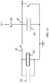
- Ferroelectric capacitor 20 includes an ideal ferroelectric capacitor 21, a non-ferroelectric capacitor 22, and a leakage resistor 23. Assume that ideal ferroelectric capacitor 21 has been partially polarized by forcing electrons onto plate 27. If the temperature increases, the remanent polarization will decrease and electrons will leave plate 27 and be stored temporarily on linear capacitor 22. This gives rise to a voltage across leakage resistor 23, which will force the electrons to move to plate 26.
- a data value to be stored is converted to a charge that is independent of the properties of the particular ferroelectric capacitor in which the charge is to be stored.
- the present invention is based on the observation that the temperature problem can be eliminated by converting a data value to a percentage of the maximum charge that can be stored in the particular ferroelectric capacitor in which the data value is to be stored.
- each state corresponds to a different fraction of Q max being stored. That is, state n corresponds to a charge of (n/Ns)Q max being stored on the ferroelectric capacitor. While this example uses a linear relationship between the fraction of the maximum charge stored and the state number, other relationships could be utilized provided the relationship between the state and the fraction of Q max stored is monotonic. The factors that determine the maximum value of Ns will be discussed in more detail below.
- the current value of Q max for that ferroelectric capacitor must be known. Hence, prior to each write, Q max must be determined.
- the data value is an integer, and hence, the data value must be converted to a fraction that is scaled by Q max to arrive at the absolute charge that is to be forced into the ferroelectric capacitor.
- FIG. 4 is a flow chart of a procedure for storing a data value, in a particular ferroelectric capacitor.
- the process begins by converting the data value to a fraction of Q max as shown at 450.
- the Q max for the particular ferroelectric capacitor in which the data value is to be stored is determined as shown at 451.
- Q max can be measured by resetting the ferroelectric capacitor to a fully polarized state in one direction and then measuring the charge that flows between the plates of the ferroelectric capacitor when the polarization is switched such that the ferroelectric capacitor is fully polarized in the opposite direction. It should be noted that at the end of this step, the ferroelectric capacitor will be fully polarized. This polarization state will be referred to as the DOWN state in the following discussion.
- the charge that is to be forced onto the ferroelectric capacitor is determined by multiplying the fraction determined in step 450 by the measured value of Q max as shown at 452. Finally, the charge determined in step 452 is forced onto the ferroelectric capacitor as shown at 453. The charge is forced onto the plate of the ferroelectric capacitor such that the charge reduces the polarization of the ferroelectric capacitor. That is, the charge partially moves the polarization of the ferroelectric capacitor in the UP direction.
- FIG. 5 is a flow chart of a procedure used to read a data value from a particular ferroelectric capacitor in a memory.
- the procedure starts by measuring the charge currently stored in the ferroelectric capacitor in question as shown at 454.
- the charge can be measured by resetting the ferroelectric capacitor to the fully polarized DOWN state and measuring the charge that flows between the plates of the ferroelectric capacitor.
- the stored charge can be measured by measuring the charge that must be added to the ferroelectric capacitor to bring the ferroelectric capacitor to a fully polarized UP state.
- Q max is measured for the ferroelectric capacitor as shown at 455. This can be accomplished by resetting the capacitor to the fully polarized UP state from the fully polarized DOWN state and then measuring the charge that flows between the plates when the polarization is flipped to the fully polarized DOWN state. Finally, the data value is determined by calculating the ratio of the measured charge to the measured value of Q max and converting that fraction to the corresponding data value as shown at 456. It should be noted that in a "read-write" operation in which a data value is read from a particular ferroelectric capacitor and then a new data value is immediately stored in that ferroelectric capacitor, the Q max value for the ferroelectric capacitor from the read operation can be used for the following write operation. In addition, the ferroelectric capacitor will already be in the fully polarized DOWN state at the end of the read operation.
- the percentage change in polarization with temperature is the same for all states.
- normalizing the charge to Q max removes variations resulting from the read and write operations being performed at different temperatures provided that once the ferroelectric capacitor is programmed, the rate of temperature change as a function of time is "small".
- the current flowing between the plates of the ferroelectric capacitor is a function of the rate of change of the dielectric temperature.
- that current must pass through leakage resistor 23 shown in Figure 3 .
- a voltage must be maintained across leakage resistor 23. The charge expelled from the ferroelectric capacitor provides this voltage.
- ferroelectric capacitor 25 is programmed in the DOWN direction as indicated by the arrow. This is accomplished by increasing the potential of plate 26 relative to plate 27 by an amount that fully polarizes the dielectric layer in the indicated direction using current-limiting source 24.
- current-limiting source 24 applies the opposite potential across ferroelectric capacitor 25; however, the current that is allowed to flow is limited so that the time to completely flip the polarization is extended beyond the time that would normally be needed if a non-limited current source were used.
- the present invention is based on the observation that ferroelectric capacitor 25 will be left in an intermediate polarization state if the process is terminated before the polarization has completely flipped.
- current-limiting source 24 is a constant current source
- the state of polarization of ferroelectric capacitor 25 will be a function of the programming time.
- a timer 28 that determines the length of time that current-limiting source 24 is on can be used to convert an input value to the intermediate polarization state.
- a digital-to-analog converter 32 is used to convert the input value to a voltage that is applied to ferroelectric capacitor 33 when switch 36 is set to connect digital-to-analog converter 32 to ferroelectric capacitor 33. This leaves a known charge on ferroelectric capacitor 33.
- switch 36 is used to connect ferroelectric capacitor 33 to ferroelectric capacitor 31, which has already been reset. Charge from ferroelectric capacitor 33 then flows into ferroelectric capacitor 31. Denote the voltage on ferroelectric capacitor 33 prior to switching by V 1 , and denote the voltage on line 34 after switching by V 2 .
- the charge transferred to ferroelectric capacitor 31 is C(V 1 -V 2 ), where C is the capacitance of ferroelectric capacitor 33. If V 1 >>V 2 , the transferred charge is proportional to the input value for a linear digital-to-analog converter. In either case, a calibration curve can be provided that maps the input state to the amount of charge that is transferred. Alternatively, digital-to-analog converter 32 can utilize a non-linear transfer function to compensate for V 2 .
- the combination of current-limiting source 24 and timer 28 shown in Figure 6 or the combination of digital-to-analog converter 32, switch 36, and ferroelectric capacitor 33 shown in Figure 7 can each be viewed as a "charge source" that transfers a known charge to the ferroelectric capacitor that is determined by the data value.
- the amount of charge transferred is independent of the hysteresis curves and saturation voltages of the ferroelectric capacitors in question, provided the charge is less than the maximum charge, Q max Consider two different ferroelectric capacitors having slightly different Q max values and/or slightly different hysteresis curves.
- the capacitors When a charge of Q is forced into each of the capacitors, the capacitors will have slightly different coordinates on their respective hysteresis curves that result from differences in properties of the ferroelectric capacitors even though the ferroelectric capacitors store the same charge. Hence, transferring a fixed charge is not equivalent to programming the ferroelectric capacitor with a voltage corresponding to a data value to be stored.
- FIG 8 illustrates a simplified circuit for reading the charge stored on the ferroelectric capacitor.
- ferroelectric capacitor 43 was reset to an UP polarization as shown by the solid arrow at 46. Data was then stored in ferroelectric capacitor 43 by storing a charge that caused the polarization to decrease in the direction of the dotted arrow.
- the goal of the readout circuit is to measure that charge when ferroelectric capacitor 43 is again reset to the UP state by providing a readout voltage that is a monotonic function of the stored charge.
- the readout operation begins with switch 41 open and switch 44 closed such that linear capacitor 42 is charged to a potential of V+. After linear capacitor 42 is charged, switch 44 is opened, and switch 41 is closed. Initially, ferroelectric capacitor 43 will have a potential of V+ across the ferroelectric capacitor. If V+ is sufficiently high, ferroelectric capacitor 43 will be reset to the UP state and the charge, Q, that was stored in ferroelectric capacitor 43 will move to linear capacitor 42, thereby lowering the potential on linear capacitor 42 by an amount equal to Q/C, where C is the capacitance of linear capacitor 42. Hence, the voltage on line 47 will be a function of the charge that was stored on ferroelectric capacitor 43.
- V+ must be greater than Q max /C + Vs where, Vs is the potential needed to fully reset ferroelectric capacitor 43. It should also be noted that ferroelectric capacitor 43 is reset in the UP state at the end of the readout operation.
- the circuit shown in Figure 8 can also be used to implement the second readout scheme if the V+ power supply is replaced by a V- power supply as shown in Figure 9 , which is a simplified readout circuit according to another embodiment of the present invention.
- This readout circuit operates in a manner analogous to that described above with reference to Figure 8 .
- switch 44 is closed while switch 41 is opened to charge linear capacitor 42.
- Switch 44 is then opened followed by switch 41 being closed.
- the potential is sufficient to cause ferroelectric capacitor 43 to become fully polarized in the DOWN direction.
- the charge needed to accomplish this is provided by linear capacitor 42.
- the difference in voltages on line 47 before and after switch 41 is closed is a measure of the charge needed to move the polarization of ferroelectric capacitor 43 from its partially polarized state to a fully DOWN state.
- ferroelectric capacitor 43 must then be reset to the UP polarization prior to reprogramming.
- Linear capacitor 22 will be referred to as a linear capacitor in the following discussion to distinguish it from an ideal ferroelectric capacitor.
- the ferroelectric capacitor has voltage applied across its plates, some charge will be stored on the linear capacitor. This charge is held on the linear capacitor by the voltage difference.
- the charge will dissipate through some leakage path, leaving just the remanent charge stored in the ferroelectric capacitor. Unless the context indicates otherwise, when this document refers to charge being stored on the ferroelectric capacitor, the charge in question is the remanent charge.
- FIG 12 illustrates the programming arrangement shown in Figure 7 with the parasitic linear capacitor explicitly shown.
- the linear capacitance is not negligible, and hence, part of the charge transferred from ferroelectric capacitor 33 to ferroelectric capacitor 31 will reside on the linear capacitor 22 associated with the ideal ferroelectric capacitor 33, and not within the ferroelectric dielectric.
- the amount of charge that was left on the linear capacitor 22 must be determined to determine the actual charge bound by the remanent polarization within the ferroelectric capacitor. If there is a residual voltage on ferroelectric capacitor 33 after switch 36 has been connected to line 34, then there is charge stored on the linear capacitor 22. The amount of charge is the voltage on the line 34 times the capacitance of linear capacitor 22.
- the parasitic linear capacitor associated with the ferroelectric capacitor can also introduce an error into the charge read from the ferroelectric capacitor.
- Figure 13 illustrates the reading scheme shown in Figure 8 with the parasitic linear capacitor associated with ferroelectric capacitor 43 explicitly shown as linear capacitor 22.
- linear capacitor 42 is charged to V+ and then connected to ferroelectric capacitor 43 by closing switch 41.
- the charge stored in ferroelectric capacitor 43 is then moved to linear capacitor 42, lowering the voltage on line 47 to V 2 .
- switch 41 is closed, the capacitance of linear capacitor 42 is increased by C L , since linear capacitor 22 is now in parallel with linear capacitor 42.
- FIG. 15 illustrates an embodiment of the present invention that utilizes a constant current source to read and write the ferroelectric capacitor.
- the parasitic linear capacitor associated with ferroelectric capacitor 25 is explicitly shown. Both the reading and writing of a data value require knowledge of Q max for ferroelectric capacitor 25.
- Q max is determined by resetting ferroelectric capacitor 25 to a fully polarized state and then measuring the charge that leaves ferroelectric capacitor 25 when ferroelectric capacitor 25 is switched to the opposite fully polarized state.
- read/write circuit 401 first applies a potential to line 402 that sets the polarization of ferroelectric capacitor to the fully polarized DOWN state as shown by the arrow next to ferroelectric capacitor 25. Any voltage across ferroelectric capacitor 25 due to charge stored on linear capacitor 22 is removed by shorting the plates of ferroelectric capacitor 25 together by closing switch 407. The charge needed to flip the polarization of ferroelectric capacitor 25 to the opposite fully polarized state is then determined by closing switch 403 and metering charge into ferroelectric capacitor 25 using current-limiting source 24. During this operation switches 404 and 407 remain open.
- ferroelectric capacitor 25 becomes fully polarized no additional charge can be stored in ferroelectric capacitor 25, and hence, the voltage on line 402 begins to rise rapidly, as the only sink for the charge is linear capacitor 22 once ferroelectric capacitor 25 has been fully polarized.
- the charge that was delivered to ferroelectric capacitor 25 and linear capacitor 22 is determined from the known current and the time of charging.
- the charge that was stored on linear capacitor 22 is determined by opening switch 403, reading the voltage on line 402, and then closing switch 404 that places a known "sharing" capacitor 408 in parallel with linear capacitor 22.
- the voltage on line 402 will decrease due to the charge now being stored on a larger capacitor (i.e., the sum of the capacitances of capacitors 22 and 408).
- the capacitance C L of linear capacitor 22 can be determined in a manner similar to that discussed above. Given that capacitance, the value of Q max can be determined from the previously measured charge that was inserted into the combination of ferroelectric capacitor 25 and linear capacitor 22.
- Data can be read from ferroelectric capacitor 25 by determining the charge that must be added to ferroelectric capacitor 25 to fully polarize ferroelectric capacitor 25 in the UP direction. This charge is the difference between the charge currently stored and Q max . Hence, given Q max , the charge stored in ferroelectric capacitor 25 can be determined.
- the procedure for measuring the charge to fully polarize ferroelectric capacitor 25 is essentially the same as that discussed above for determining Q max , except that the polarization of ferroelectric capacitor 25 is not altered prior to adding charge via current-limiting source 24.
- C L is computed at each read and write and for each ferroelectric capacitor in a memory array.
- the need to correct for C L depends on the number of levels being stored in a ferroelectric capacitor and the amount of charge that is stored on the parasitic linear capacitor during reading and writing operations.
- the need to calculate C L at each read and write depends on the degree of variability of C L over the memory array and with temperature.
- C L introduces an error in the charge being programmed into a ferroelectric capacitor and the charge being read from the ferroelectric capacitor.
- the successive polarization states are characterized by a charge that is stored for each state. If the charge error is small compared to the difference in charge between successive states, no further correction is required. In one aspect of the invention, the error will be considered small if the error is less than 0.25 times the difference in stored charge between successive levels.
- C L is assumed to be zero for all ferroelectric capacitors. If this leads to an error for a specific memory design, then the next level of correction would be to measure C L for each ferroelectric capacitor in the array at the time the array is manufactured and store an average C L value as part of the array calibration. In this case, the errors are determined by the variability of C L over the array and with temperature. If the resulting errors are still too large, then embodiments in which C L is measured at each read and write can be utilized.
- Ferroelectric memory 50 includes a plurality of ferroelectric memory cells organized into a plurality of rows and columns.
- a typical ferroelectric memory cell is labeled at 51.
- Each ferroelectric memory cell includes a ferroelectric capacitor 52 and an interface circuit 53. All of the ferroelectric memory cells in a row are processed in parallel during read and write operations.
- the row to be processed is selected by a row select circuit 56 that operates a plurality of row select buses 54 that also include conductors for sequencing the row processing operations during reading and writing.
- Each ferroelectric memory cell in a given column is connected to two column buses shown at 58 and 59.
- Column bus 58 is used to readout the data stored in the ferroelectric capacitor in the ferroelectric memory cell being processed, and column bus 59 is used to program the ferroelectric capacitor in a new analog value.
- Each ferroelectric capacitor can be programmed to be in one of N states, where N>2.
- the state of a ferroelectric capacitor in a row being processed is ascertained by generating a signal on column bus 58 indicative of the amount of charge that was stored in that ferroelectric capacitor. This state is read using circuit 62.
- the state of a ferroelectric capacitor in a row being processed is set by applying signals to column bus 59 connected to that cell via write circuit 61. The signals cause a predetermined amount of charge that is related to the value to be stored in the ferroelectric memory cell to be stored in the ferroelectric capacitor in that ferroelectric memory cell.
- Data that is read out of a row is stored in a row buffer 55.
- the data is converted from an analog signal representing the charge stored in the corresponding ferroelectric capacitors to a digital value. Since the readout process is destructive, this data must be restored to the row with a write operation even in cases in which no changes in the data are to be made. If changes are to be made, the changes are entered into row buffer 55 after the ferroelectric memory cells in the row have been reset. The data in row buffer 55 is then converted to a charge that is stored in the corresponding ferroelectric capacitors.
- the read and write operations utilize a controller 57 that receives an address (ADDR), operation code (OPCODE), and data to be written to the ferroelectric memory cell(s) specified in the address. Data from the indicated address is output on the data lines. Row select circuit 56 applies the appropriate signals to the row select bus specified by the address.
- ADDR address
- OPCODE operation code
- Row select circuit 56 applies the appropriate signals to the row select bus specified by the address.
- Ferroelectric memory 50 includes two column buses for each column of memory cells, one for reading and one for writing. This arrangement simplifies the following discussion of the detailed embodiments. However embodiments in which only one column bus is needed can also be constructed.
- FIG 11 illustrates one embodiment of a ferroelectric memory according to the present invention that utilizes the storage scheme discussed above in which data is readout by measuring the amount of charge that was stored in the ferroelectric capacitor during the writing operation.
- the four row lines R1-R4 are part of the row bus corresponding to the row of memory cells in which ferroelectric memory cell 310 is located.
- Both the read and write operations require a knowledge of Q max for ferroelectric capacitor 82 at the time of reading or writing.
- Q max can be measured for ferroelectric capacitor 82 by programming ferroelectric capacitor 82 to the fully DOWN state and then requesting readout circuit 74 to measure the charge that is released when ferroelectric capacitor 82 is subjected to a voltage that causes ferroelectric capacitor 82 to be fully polarized in the UP state. This operation leaves ferroelectric capacitor 82 polarized in the fully UP state.
- the value of Q max is communicated to write circuit 75, which then calculates the charge needed to program ferroelectric capacitor 82 from the received data value and the maximum number of data states that are to be stored in ferroelectric capacitor 82.
- a value is written into ferroelectric memory cell 310 by placing gate 84 in the conductive state and gate 86 in a nonconductive state.
- Capacitor 77 is then charged to a potential that will result in a charge having a value corresponding to the data being written being transferred to ferroelectric capacitor 82 when gate 76 is placed in a conducting state by write circuit 75.
- the voltage on capacitor 77 is less than V 2 , by an amount that depends on the data value to be written.
- ferroelectric capacitor 82 When ferroelectric capacitor 82 is connected to write line 73 through gate 84, the top plate will be at a potential that is less than the bottom plate, which is held at V 2 , and hence, the write operation reverses part of the polarization created by the reset operation.
- Q max In a readout operation, Q max must be determined after the charge currently stored in ferroelectric capacitor 82 is determined.
- Data is read out of ferroelectric memory cell 310 in a three-step process by readout circuit 74 that is connected to read line 72 by gate 88.
- capacitor 83 is charged to V 1 while being isolated from ferroelectric capacitor 82 by gate 86.
- Gate 85 is utilized to connect capacitor 83 to V 1 .
- V 1 is greater than V 2 by an amount that allows the maximum design charge to be transferred to capacitor 83 and still have the top plate of capacitor 83 at a voltage greater than V 2 .
- the final voltage on capacitor 83 is amplified by source follower 87 and readout by readout circuit 74 which stores the voltage on a capacitor within readout circuit 74.
- gate 86 is placed in a conducting state with gate 84 off which applies voltage on capacitor 83 across ferroelectric capacitor 82. This resets ferroelectric capacitor 82 and causes the charge stored in ferroelectric capacitor 82 to be released, which, in turn, lowers the voltage at the gate of source follower 87. This voltage is then read by readout circuit 74 and subtracted from the voltage stored previously to arrive at a voltage difference that is indicative of the charge that was released by ferroelectric capacitor 82. Finally, Q max is determined. Ferroelectric capacitor 82 is programmed to the fully polarized DOWN state again and the readout process is repeated to determine Q max . The ratio of Q max to the Q measured from the first two steps is then digitized to provide the output data.
- an optional, shorting circuit 89 is connected between the plates of ferroelectric capacitor 82 to limit the voltage across ferroelectric capacitor 82 when no voltage is applied to ferroelectric memory cell 310.
- each transistor in shorting circuit 89 is normally conducting, but turns off if a positive voltage is applied across the gate of the transistor.
- the voltage on line 89a can swing both above and below V 2 . If the voltage is above V 2 one of the transistors will be off. If it goes below V 2 , the other transistor will be off. Hence, the plates of ferroelectric capacitor 82 will not be shorted during reading and writing.
- V 2 power line and R1 will be at zero volts, and hence all three of the transistors will be conducting, and the plates will be shorted to prevent temperature changes from inducing voltages across ferroelectric capacitor 82 that are sufficient to alter the stored data value.
- the read and write times of a memory according to the present invention will be much shorter than the time over which a temperature change occurs.
- shorting circuit 89 can be replaced by a properly sized resistor.
- the resistor would need to have an RC time constant that is large compared to the read and write times.
- the capacitance is the parasitic capacitance of ferroelectric capacitor 82.
- the resistor would need to be small enough to allow any charge leaving ferroelectric capacitor 82 to move to the opposite plate of ferroelectric capacitor 82 without generating a voltage across the resistor that is sufficient to change the data value stored in ferroelectric capacitor 82.
- the problem with data being disturbed during a temperature shift depends on the rate of temperature change of the ferroelectric capacitor. If the rate of temperature change can be limited, the problems associated with data alteration can be significantly reduced. Typically, the temperature change of most concern is a shift in the air temperature.
- the rate of temperature change of the ferroelectric capacitor depends on the thermal mass of the memory circuit. If the thermal mass is sufficiently large, or a thermal resistance layer separates the memory circuit from the environment, the rate at which the unpowered circuit can be shifted in temperature can be kept below the rate that would disturb the data for any given memory design.
- FIG 14 is a cross-sectional view of memory according to one embodiment of the present invention that is packaged in a manner that reduces the rate at which the temperature of the memory can be changed.
- a memory circuit 301 is sandwiched between layers 302 and 303.
- layers 303 and 302 are thermal conductors with sufficient thermal mass to reduce the rate of temperature change of memory circuit 301 while allowing heat to flow from memory circuit 301 to the outside environment.
- This embodiment allows the heat generated in memory circuit 301 during powered operation to escape while limiting the rate of temperature change, since layers 302 and 303 act as heat sinks.
- memory circuit 301 or layers 302 and 303 include insulating layers that prevent shorts in memory circuit 301.
- layers 302 and 303 are thermal insulators that provide a sufficient thermal resistance to limit the rate of temperature change during periods in which memory circuit 301 is not powered.
- memory systems that split the read and write functions into separate components can also be constructed.
- the system could include three components, a write unit, a memory module that includes the ferroelectric capacitors, and a read unit.
- a removable memory module is adapted to plug into the write unit for programming. The removable module would then be removed and transport to the read unit for reading.
- This type of system is adapted for situations in which a large number of write stations accumulate data over a period of time.
- the write modules are then sent to a common read station that is part of a processing system the reads out the data and processes that data.
Landscapes
- Engineering & Computer Science (AREA)
- Computer Hardware Design (AREA)
- Power Engineering (AREA)
- Microelectronics & Electronic Packaging (AREA)
- Databases & Information Systems (AREA)
- Dram (AREA)
- Semiconductor Memories (AREA)
Claims (15)
- Ferroelektrischer Speicher (50, 70), der Folgendes umfasst:eine ferroelektrische Speicherzelle (310), die einen ferroelektrischen Kondensator umfasst, wobei eine maximale remanente Ladung, Qmax, in dem ferroelektrischen Kondensator gespeichert werden kann; undeine Schreibschaltung (75), die einen Schreibdatenwert empfängt, der aus einem Satz von mehr als zwei Werten zur Speicherung in dem ferroelektrischen Kondensator ausgewählt ist, dadurch gekennzeichnet, dass die Schreibschaltung Qmax für den ferroelektrischen Kondensator (82) misst und eine erste Ladung bestimmt, die ein Bruchteil des gemessenen Qmax ist, wobei die erste Ladung durch den Schreibdatenwert bestimmt wird, wobei die Schreibschaltung bewirkt, dass die erste Ladung in dem ferroelektrischen Kondensator gespeichert wird.
- Ferroelektrischer Speicher nach Anspruch 1, der ferner eine Leseschaltung (74) umfasst, die einen gespeicherten Datenwert ermittelt, der in dem ferroelektrischen Kondensator gespeichert ist, wobei die Leseschaltung eine zweite in dem ferroelektrischen Kondensator gespeicherte Ladung misst, Qmax für den ferroelektrischen Kondensator misst und den gespeicherten Datenwert aus der zweiten Ladung und dem gemessenen Qmax bestimmt.
- Ferroelektrischer Speicher nach Anspruch 1, der ferner Folgendes umfasst:eine Vielzahl von ferroelektrischen Speicherzellen (51), wobei jede ferroelektrische Speicherzelle einen ferroelektrischen Kondensator (52) umfasst, gekennzeichnet durch eine maximale remanente Ladung, Qmax, die in diesem ferroelektrischen Kondensator gespeichert werden kann; undeine Speicherzellenauswahlschaltung (56), die einen der ferroelektrischen Kondensatoren auswählt, wobei die Schreibschaltung (61) einen dritten Datenwert empfängt, der aus einem Satz mit mehr als zwei Werten zur Speicherung in dem einen der ferroelektrischen Kondensatoren ausgewählt ist, wobei die Schreibschaltung Qmax für den einen der ferroelektrischen Kondensatoren misst, eine dritte Ladung bestimmt, die ein Bruchteil des gemessenen Qmax ist, und bewirkt, dass die dritte Ladung in dem einen der ferroelektrischen Kondensatoren gespeichert wird, wobei die dritte Ladung durch den dritten Datenwert bestimmt wird.
- Ferroelektrischer Speicher nach Anspruch 3, der ferner eine Leseschaltung (62) umfasst, die einen dritten Datenwert bestimmt, der in dem einen der ferroelektrischen Kondensatoren gespeichert ist, wobei die Leseschaltung eine in dem einen der ferroelektrischen Kondensatoren gespeicherte vierte Ladung misst, Qmax für den einen der ferroelektrischen Kondensatoren misst und den dritten Datenwert aus einem Verhältnis der vierten Ladung und dem gemessenen Qmax bestimmt.
- Ferroelektrischer Speicher nach Anspruch 1, wobei der ferroelektrische Kondensator einen parasitären linearen Kondensator (22) umfasst und wobei die Schreibschaltung eine fünfte Ladung misst, die von dem ferroelektrischen Kondensator fließt, wenn der ferroelektrische Kondensator von einem vollständig polarisierten Zustand in einer Richtung zu einem vollständig polarisierten Zustand in einer entgegengesetzten Richtung geschaltet wird, wobei die fünfte Ladung um eine parasitäre Ladung korrigiert wird, die auf dem parasitären linearen Kondensator gespeichert wurde.
- Ferroelektrischer Speicher nach Anspruch 2, wobei der ferroelektrische Kondensator einen parasitären linearen Kondensator (22) umfasst und wobei die Leseschaltung eine fünfte Ladung misst, die von dem ferroelektrischen Kondensator fließt, wenn der ferroelektrische Kondensator von einem vollständig polarisierten Zustand in einer Richtung zu einem vollständig polarisierten Zustand in einer entgegengesetzten Richtung geschaltet wird, wobei die fünfte Ladung um eine parasitäre Ladung korrigiert wird, die auf dem parasitären linearen Kondensator gespeichert wurde.
- Ferroelektrischer Speicher nach Anspruch 2, wobei der ferroelektrische Kondensator durch erste und zweite Platten gekennzeichnet ist, die ein ferroelektrisches dielektrisches Material dazwischen umfassen, wobei der ferroelektrische Speicher eine Kurzschlussschaltung (89) umfasst, die die erste und die zweite Platte elektrisch verbindet, wenn die Schreibschaltung (75) nicht bewirkt, dass die erste Ladung in dem ferroelektrischen Kondensator (82) gespeichert wird, oder die Leseschaltung (74) nicht die zweite Ladung misst, wobei die Kurzschlussschaltung außer Betrieb ist, wenn die Leseschaltung die Messung der zweiten Ladung bewirkt oder die Schreibschaltung die Speicherung der ersten Ladung in dem ferroelektrischen Kondensator bewirkt.
- Ferroelektrischer Speicher nach Anspruch 2, der gekennzeichnet durch eine maximale Temperaturänderungsrate ist, für die der ferroelektrische Speicher ausgelegt ist, und wobei der ferroelektrische Kondensator ein thermisches Gehäuse (302, 303) umfasst, das Temperaturänderungen des ferroelektrischen Kondensators auf die maximale Rate begrenzt.
- Ferroelektrischer Speicher nach Anspruch 3, wobei die Speicherzellenauswahlschaltung Folgendes umfasst:eine Schreibleitung (59) ;eine Leseleitung (58); undeine Vielzahl von Auswahlbusleitungen (54) für ferroelektrische Speicherzellen, wobei eine der Auswahlbusleitungen jeder der Vielzahl von ferroelektrischen Speicherzellen entspricht, wobei jede der mehreren ferroelektrischen Speicherzellen erste und zweite Gates (88, 84) zum Verbinden der ferroelektrischen Speicherzelle mit der Leseleitung bzw. der Schreibleitung als Reaktion auf Signale auf der einen der Auswahlbusleitungen für ferroelektrische Speicherzellen, die dieser ferroelektrischen Speicherzelle entspricht, umfasst.
- Ferroelektrischer Speicher nach Anspruch 3, wobei jeder der ferroelektrischen Kondensatoren durch erste und zweite leitende Platten gekennzeichnet ist und jede der ferroelektrischen Speicherzellen einen Entladungspfad (89) umfasst, der die ersten und zweiten leitenden Platten verbindet, wobei der Entladepfad eine Impedanz aufweist, die verhindert, dass eine Spannung zwischen der ersten und der zweiten leitenden Platte erzeugt wird, die größer ist als eine Störspannung, wenn die ferroelektrische Speicherzelle nicht ausgewählt ist, wobei der Entladungspfad eine Impedanz aufweist, die größer ist als eine Auswahlimpedanz, wenn die ferroelektrische Speicherzelle ausgewählt ist, wobei die Störspannung kleiner ist als eine Spannung, die eine in dem ferroelektrischen Kondensator gespeicherte Ladung um mehr als einen Betrag ändern würde, der einen in dem ferroelektrischen Kondensator gespeicherten Datenwert ändern würde, und die Auswahlimpedanz größer ist als eine Impedanz, die einen Fehler beim Lesen eines Datenwertes aus dem ferroelektrischen Kondensator oder beim Schreiben eines Datenwertes in den ferroelektrischen Kondensator verursachen würde.
- Verfahren zum Betreiben einer ferroelektrischen Speicherzelle, die einen ferroelektrischen Kondensator (82) umfasst, wobei der ferroelektrische Kondensator eine maximale remanente Ladung, Qmax, umfasst, die in dem ferroelektrischen Kondensator gespeichert werden kann, wobei das Verfahren Folgendes umfasst:
eine Schreiboperation, die Folgendes umfasst:
Empfangen eines Schreibdatenwertes, der in dem ferroelektrischen Kondensator gespeichert werden soll, wobei der Schreibdatenwert aus einem Satz mit mehr als zwei Werten ausgewählt wird, gekennzeichnet durch:Messen von Qmax für den ferroelektrischen Kondensator (451);Bestimmen einer ersten Ladung, die ein Bruchteil des gemessenen Qmax ist, wobei die Ladung durch den Schreibdatenwert bestimmt wird; undBewirken, dass die erste Ladung in dem ferroelektrischen Kondensator (453) gespeichert wird. - Verfahren nach Anspruch 11, wobei Qmax vor der Durchführung jedes Schreibvorgangs gemessen wird.
- Verfahren nach Anspruch 11, das ferner eine Leseoperation umfasst, wobei die Leseoperation Folgendes umfasst:Bestimmen einer zweiten in dem ferroelektrischen Kondensator (454) gespeicherten Ladung;Bestimmen von Qmax für den ferroelektrischen Kondensator (455) ;Umwandeln des bestimmten Qyax und der zweiten Ladung in einen Datenwert (456), wobei der Datenwert aus einem Satz mit mehr als zwei Werten ausgewählt wird.
- Verfahren nach Anspruch 13, wobei der ferroelektrische Kondensator einen parasitären linearen Kondensator (22) umfasst und wobei das Bestimmen von Qmax das Messen einer dritten Ladung umfasst, die von dem ferroelektrischen Kondensator fließt, wenn der ferroelektrische Kondensator von einem vollständig polarisierten Zustand in einer Richtung zu einem vollständig polarisierten Zustand in einer entgegengesetzten Richtung geschaltet wird, wobei die dritte Ladung um eine parasitäre Ladung korrigiert wird, die auf dem parasitären linearen Kondensator gespeichert wurde.
- Verfahren nach Anspruch 11, wobei der ferroelektrische Kondensator durch eine erste und eine zweite leitende Platte gekennzeichnet ist, wobei das Verfahren ferner Folgendes umfasst:
Bereitstellen eines Entladungspfades, der die erste und die zweite leitende Platte verbindet, wobei der Entladungspfad (89) eine Impedanz aufweist, die verhindert, dass eine Spannung zwischen der ersten und der zweiten leitenden Platte erzeugt wird, die größer ist als eine Störspannung, wenn die ferroelektrische Speicherzelle keinen Lesevorgang oder Schreibvorgang durchläuft, wobei die Störspannung kleiner ist als eine Spannung, die eine in dem ferroelektrischen Kondensator gespeicherte Ladung um mehr als einen Betrag ändern würde, der einen in dem ferroelektrischen Kondensator gespeicherten Datenwert ändern würde, und der Entladungspfad eine Impedanz aufweist, die größer ist als eine Impedanz, die einen Fehler in dem Lesevorgang oder dem Schreibvorgang verursachen würde, wenn der ferroelektrische Kondensator den Lesevorgang oder den Schreibvorgang durchläuft.
Applications Claiming Priority (2)
| Application Number | Priority Date | Filing Date | Title |
|---|---|---|---|
| US15/252,146 US9697882B1 (en) | 2016-08-30 | 2016-08-30 | Analog ferroelectric memory with improved temperature range |
| PCT/US2017/048958 WO2018044815A1 (en) | 2016-08-30 | 2017-08-28 | Analog ferroelectric memory with improved temperature range |
Publications (4)
| Publication Number | Publication Date |
|---|---|
| EP3482397A1 EP3482397A1 (de) | 2019-05-15 |
| EP3482397A4 EP3482397A4 (de) | 2020-04-01 |
| EP3482397B1 true EP3482397B1 (de) | 2023-08-09 |
| EP3482397C0 EP3482397C0 (de) | 2023-08-09 |
Family
ID=59152455
Family Applications (1)
| Application Number | Title | Priority Date | Filing Date |
|---|---|---|---|
| EP17847321.1A Active EP3482397B1 (de) | 2016-08-30 | 2017-08-28 | Analoger ferroelektrischer speicher mit verbessertem temperaturbereich |
Country Status (6)
| Country | Link |
|---|---|
| US (1) | US9697882B1 (de) |
| EP (1) | EP3482397B1 (de) |
| JP (1) | JP6963323B2 (de) |
| KR (1) | KR102379736B1 (de) |
| CN (1) | CN109643569B (de) |
| WO (1) | WO2018044815A1 (de) |
Families Citing this family (26)
| Publication number | Priority date | Publication date | Assignee | Title |
|---|---|---|---|---|
| US10282108B2 (en) * | 2016-08-31 | 2019-05-07 | Micron Technology, Inc. | Hybrid memory device using different types of capacitors |
| CN110858723B (zh) * | 2018-08-24 | 2025-10-10 | 瑞萨设计(英国)有限公司 | 用于电荷再循环的方法和装置 |
| US10796729B2 (en) * | 2019-02-05 | 2020-10-06 | Micron Technology, Inc. | Dynamic allocation of a capacitive component in a memory device |
| KR102679871B1 (ko) | 2019-04-03 | 2024-06-28 | 엘지디스플레이 주식회사 | 표시장치 |
| US10944404B1 (en) | 2019-12-27 | 2021-03-09 | Kepler Computing, Inc. | Low power ferroelectric based majority logic gate adder |
| US11374574B2 (en) | 2019-12-27 | 2022-06-28 | Kepler Computing Inc. | Linear input and non-linear output threshold logic gate |
| US11283453B2 (en) | 2019-12-27 | 2022-03-22 | Kepler Computing Inc. | Low power ferroelectric based majority logic gate carry propagate and serial adder |
| US11018672B1 (en) | 2019-12-27 | 2021-05-25 | Kepler Computing Inc. | Linear input and non-linear output majority logic gate |
| US11462282B2 (en) * | 2020-04-01 | 2022-10-04 | Taiwan Semiconductor Manufacturing Co., Ltd. | Semiconductor memory structure |
| US11165430B1 (en) | 2020-12-21 | 2021-11-02 | Kepler Computing Inc. | Majority logic gate based sequential circuit |
| US11381244B1 (en) | 2020-12-21 | 2022-07-05 | Kepler Computing Inc. | Low power ferroelectric based majority logic gate multiplier |
| US11290112B1 (en) | 2021-05-21 | 2022-03-29 | Kepler Computing, Inc. | Majority logic gate based XOR logic gate with non-linear input capacitors |
| US11705906B1 (en) | 2021-05-21 | 2023-07-18 | Kepler Computing Inc. | Majority logic gate having ferroelectric input capacitors and a pulsing scheme coupled to a conditioning logic |
| US11303280B1 (en) | 2021-08-19 | 2022-04-12 | Kepler Computing Inc. | Ferroelectric or paraelectric based sequential circuit |
| US12524204B1 (en) | 2021-09-02 | 2026-01-13 | Kepler Computing Inc. | Ferroelectric or paraelectric based low power multiplier |
| US12118327B1 (en) | 2021-09-02 | 2024-10-15 | Kepler Computing Inc. | Ripple carry adder with inverted ferroelectric or paraelectric based adders |
| US12316319B1 (en) | 2021-12-14 | 2025-05-27 | Kepler Computing Inc. | Multi-function linear threshold gate with input based adaptive threshold |
| US11705905B1 (en) | 2021-12-14 | 2023-07-18 | Kepler Computing, Inc. | Multi-function ferroelectric threshold gate with input based adaptive threshold |
| US11664370B1 (en) | 2021-12-14 | 2023-05-30 | Kepler Corpating inc. | Multi-function paraelectric threshold gate with input based adaptive threshold |
| US11716085B1 (en) | 2021-12-23 | 2023-08-01 | Kepler Computing, Inc. | Pull-up and pull-down networks controlled asynchronously by threshold gate logic |
| US11855627B1 (en) | 2022-01-13 | 2023-12-26 | Kepler Computing Inc. | Asynchronous consensus circuit using multi-function threshold gate with input based adaptive threshold |
| US12379898B1 (en) | 2022-02-07 | 2025-08-05 | Kepler Computing Inc. | Asynchronous full-adder with majority or minority gates to generate sum false output |
| US11750197B1 (en) | 2022-04-20 | 2023-09-05 | Kepler Computing Inc. | AND-OR-invert logic based on a mix of majority OR minority logic gate with non-linear input capacitors and other logic gates |
| US20240274651A1 (en) | 2023-02-10 | 2024-08-15 | Kepler Computing Inc. | Method of forming stacked capacitors through wafer bonding |
| US11765908B1 (en) | 2023-02-10 | 2023-09-19 | Kepler Computing Inc. | Memory device fabrication through wafer bonding |
| US12445134B1 (en) | 2023-12-20 | 2025-10-14 | Kepler Computing Inc. | Diode connected non-linear input capacitors based majority gate |
Family Cites Families (18)
| Publication number | Priority date | Publication date | Assignee | Title |
|---|---|---|---|---|
| US3280332A (en) * | 1964-02-25 | 1966-10-18 | Gen Telephone & Elect | Ferroelectric amplifier for driving light emitting load |
| US5524092A (en) * | 1995-02-17 | 1996-06-04 | Park; Jea K. | Multilayered ferroelectric-semiconductor memory-device |
| US5532953A (en) * | 1995-03-29 | 1996-07-02 | Ramtron International Corporation | Ferroelectric memory sensing method using distinct read and write voltages |
| US6008659A (en) * | 1996-03-15 | 1999-12-28 | Ramtron International Corporation | Method of measuring retention performance and imprint degradation of ferroelectric films |
| US5966318A (en) * | 1996-12-17 | 1999-10-12 | Raytheon Company | Nondestructive readout memory utilizing ferroelectric capacitors isolated from bitlines by buffer amplifiers |
| JP3966593B2 (ja) * | 1997-12-26 | 2007-08-29 | ローム株式会社 | 強誘電体回路シミュレーション装置 |
| US6449184B2 (en) * | 2000-06-19 | 2002-09-10 | Matsushita Electric Industrial Co., Ltd. | Method for driving semiconductor memory |
| JP2002269973A (ja) * | 2000-12-28 | 2002-09-20 | Seiko Epson Corp | 強誘電体メモリ装置およびその駆動方法 |
| KR100400773B1 (ko) * | 2001-06-29 | 2003-10-08 | 주식회사 하이닉스반도체 | 강유전체 랜덤 억세스 메모리의 강유전 캐패시터 테스트회로 |
| KR100487417B1 (ko) * | 2001-12-13 | 2005-05-03 | 주식회사 하이닉스반도체 | 불휘발성 강유전체 메모리 장치 및 그를 이용한멀티플-비트 데이타의 라이트 및 리드 방법 |
| US6856534B2 (en) * | 2002-09-30 | 2005-02-15 | Texas Instruments Incorporated | Ferroelectric memory with wide operating voltage and multi-bit storage per cell |
| JP4256670B2 (ja) * | 2002-12-10 | 2009-04-22 | 富士通株式会社 | 容量素子、半導体装置およびその製造方法 |
| US7085150B2 (en) * | 2004-12-20 | 2006-08-01 | Texas Instruments Incorporated | Methods for enhancing performance of ferroelectic memory with polarization treatment |
| JP4946214B2 (ja) * | 2006-06-30 | 2012-06-06 | 富士通セミコンダクター株式会社 | 半導体装置の製造方法 |
| JP2010140557A (ja) * | 2008-12-11 | 2010-06-24 | Toshiba Corp | 不揮発性半導体記憶装置 |
| US7990749B2 (en) | 2009-06-08 | 2011-08-02 | Radiant Technology, Inc. | Variable impedance circuit controlled by a ferroelectric capacitor |
| US8760907B2 (en) * | 2010-11-30 | 2014-06-24 | Radiant Technologies, Inc. | Analog memories utilizing ferroelectric capacitors |
| US9324405B2 (en) * | 2010-11-30 | 2016-04-26 | Radiant Technologies, Inc. | CMOS analog memories utilizing ferroelectric capacitors |
-
2016
- 2016-08-30 US US15/252,146 patent/US9697882B1/en active Active
-
2017
- 2017-08-28 CN CN201780052709.8A patent/CN109643569B/zh not_active Expired - Fee Related
- 2017-08-28 EP EP17847321.1A patent/EP3482397B1/de active Active
- 2017-08-28 JP JP2019510821A patent/JP6963323B2/ja not_active Expired - Fee Related
- 2017-08-28 KR KR1020197007433A patent/KR102379736B1/ko not_active Expired - Fee Related
- 2017-08-28 WO PCT/US2017/048958 patent/WO2018044815A1/en not_active Ceased
Also Published As
| Publication number | Publication date |
|---|---|
| KR20190039261A (ko) | 2019-04-10 |
| US9697882B1 (en) | 2017-07-04 |
| CN109643569A (zh) | 2019-04-16 |
| JP6963323B2 (ja) | 2021-11-05 |
| KR102379736B1 (ko) | 2022-03-29 |
| EP3482397A4 (de) | 2020-04-01 |
| CN109643569B (zh) | 2023-01-17 |
| WO2018044815A1 (en) | 2018-03-08 |
| EP3482397C0 (de) | 2023-08-09 |
| JP2019531570A (ja) | 2019-10-31 |
| EP3482397A1 (de) | 2019-05-15 |
Similar Documents
| Publication | Publication Date | Title |
|---|---|---|
| EP3482397B1 (de) | Analoger ferroelektrischer speicher mit verbessertem temperaturbereich | |
| KR102316937B1 (ko) | 셀렉터 전압 보상 기능을 갖는 자기 랜덤-액세스 메모리 | |
| US9496019B2 (en) | CMOS analog memories utilizing ferroelectric capacitors | |
| US6791874B2 (en) | Memory device capable of calibration and calibration methods therefor | |
| US8760907B2 (en) | Analog memories utilizing ferroelectric capacitors | |
| EP0956561B1 (de) | Differentielle flash-speicherzelle und betriebsverfahren dafür | |
| EP2290658B1 (de) | Stromsparendes Lesen in magnetischen Speicheranordnungen | |
| US7800968B2 (en) | Symmetric differential current sense amplifier | |
| US10120816B2 (en) | Bad column management with data shuffle in pipeline | |
| EP3198604B1 (de) | Cmos-analogspeicher mit ferroelektrischen kondensatoren | |
| TW201939495A (zh) | 用於預充電記憶體單元之技術 | |
| KR20200036040A (ko) | 랜덤 액세스 및 강유전체 메모리를 위한 웨어 레벨링 | |
| EP4396817A1 (de) | Kaskoden zur entwicklung von signalen auf deckebene |
Legal Events
| Date | Code | Title | Description |
|---|---|---|---|
| STAA | Information on the status of an ep patent application or granted ep patent |
Free format text: STATUS: THE INTERNATIONAL PUBLICATION HAS BEEN MADE |
|
| PUAI | Public reference made under article 153(3) epc to a published international application that has entered the european phase |
Free format text: ORIGINAL CODE: 0009012 |
|
| STAA | Information on the status of an ep patent application or granted ep patent |
Free format text: STATUS: REQUEST FOR EXAMINATION WAS MADE |
|
| 17P | Request for examination filed |
Effective date: 20190205 |
|
| AK | Designated contracting states |
Kind code of ref document: A1 Designated state(s): AL AT BE BG CH CY CZ DE DK EE ES FI FR GB GR HR HU IE IS IT LI LT LU LV MC MK MT NL NO PL PT RO RS SE SI SK SM TR |
|
| AX | Request for extension of the european patent |
Extension state: BA ME |
|
| DAV | Request for validation of the european patent (deleted) | ||
| DAX | Request for extension of the european patent (deleted) | ||
| A4 | Supplementary search report drawn up and despatched |
Effective date: 20200302 |
|
| RIC1 | Information provided on ipc code assigned before grant |
Ipc: G11C 11/16 20060101ALI20200225BHEP Ipc: G11C 11/4096 20060101ALI20200225BHEP Ipc: G11C 11/22 20060101AFI20200225BHEP Ipc: G11C 11/56 20060101ALI20200225BHEP Ipc: G11C 11/419 20060101ALI20200225BHEP |
|
| STAA | Information on the status of an ep patent application or granted ep patent |
Free format text: STATUS: EXAMINATION IS IN PROGRESS |
|
| 17Q | First examination report despatched |
Effective date: 20210902 |
|
| GRAP | Despatch of communication of intention to grant a patent |
Free format text: ORIGINAL CODE: EPIDOSNIGR1 |
|
| STAA | Information on the status of an ep patent application or granted ep patent |
Free format text: STATUS: GRANT OF PATENT IS INTENDED |
|
| INTG | Intention to grant announced |
Effective date: 20230310 |
|
| GRAS | Grant fee paid |
Free format text: ORIGINAL CODE: EPIDOSNIGR3 |
|
| GRAA | (expected) grant |
Free format text: ORIGINAL CODE: 0009210 |
|
| STAA | Information on the status of an ep patent application or granted ep patent |
Free format text: STATUS: THE PATENT HAS BEEN GRANTED |
|
| AK | Designated contracting states |
Kind code of ref document: B1 Designated state(s): AL AT BE BG CH CY CZ DE DK EE ES FI FR GB GR HR HU IE IS IT LI LT LU LV MC MK MT NL NO PL PT RO RS SE SI SK SM TR |
|
| REG | Reference to a national code |
Ref country code: GB Ref legal event code: FG4D |
|
| REG | Reference to a national code |
Ref country code: CH Ref legal event code: EP |
|
| REG | Reference to a national code |
Ref country code: DE Ref legal event code: R096 Ref document number: 602017072587 Country of ref document: DE |
|
| REG | Reference to a national code |
Ref country code: IE Ref legal event code: FG4D |
|
| U01 | Request for unitary effect filed |
Effective date: 20230905 |
|
| U07 | Unitary effect registered |
Designated state(s): AT BE BG DE DK EE FI FR IT LT LU LV MT NL PT SE SI Effective date: 20230913 |
|
| PG25 | Lapsed in a contracting state [announced via postgrant information from national office to epo] |
Ref country code: GR Free format text: LAPSE BECAUSE OF FAILURE TO SUBMIT A TRANSLATION OF THE DESCRIPTION OR TO PAY THE FEE WITHIN THE PRESCRIBED TIME-LIMIT Effective date: 20231110 |
|
| PG25 | Lapsed in a contracting state [announced via postgrant information from national office to epo] |
Ref country code: IS Free format text: LAPSE BECAUSE OF FAILURE TO SUBMIT A TRANSLATION OF THE DESCRIPTION OR TO PAY THE FEE WITHIN THE PRESCRIBED TIME-LIMIT Effective date: 20231209 |
|
| PG25 | Lapsed in a contracting state [announced via postgrant information from national office to epo] |
Ref country code: RS Free format text: LAPSE BECAUSE OF FAILURE TO SUBMIT A TRANSLATION OF THE DESCRIPTION OR TO PAY THE FEE WITHIN THE PRESCRIBED TIME-LIMIT Effective date: 20230809 Ref country code: NO Free format text: LAPSE BECAUSE OF FAILURE TO SUBMIT A TRANSLATION OF THE DESCRIPTION OR TO PAY THE FEE WITHIN THE PRESCRIBED TIME-LIMIT Effective date: 20231109 Ref country code: IS Free format text: LAPSE BECAUSE OF FAILURE TO SUBMIT A TRANSLATION OF THE DESCRIPTION OR TO PAY THE FEE WITHIN THE PRESCRIBED TIME-LIMIT Effective date: 20231209 Ref country code: HR Free format text: LAPSE BECAUSE OF FAILURE TO SUBMIT A TRANSLATION OF THE DESCRIPTION OR TO PAY THE FEE WITHIN THE PRESCRIBED TIME-LIMIT Effective date: 20230809 Ref country code: GR Free format text: LAPSE BECAUSE OF FAILURE TO SUBMIT A TRANSLATION OF THE DESCRIPTION OR TO PAY THE FEE WITHIN THE PRESCRIBED TIME-LIMIT Effective date: 20231110 |
|
| PG25 | Lapsed in a contracting state [announced via postgrant information from national office to epo] |
Ref country code: PL Free format text: LAPSE BECAUSE OF FAILURE TO SUBMIT A TRANSLATION OF THE DESCRIPTION OR TO PAY THE FEE WITHIN THE PRESCRIBED TIME-LIMIT Effective date: 20230809 |
|
| REG | Reference to a national code |
Ref country code: CH Ref legal event code: PL |
|
| PG25 | Lapsed in a contracting state [announced via postgrant information from national office to epo] |
Ref country code: ES Free format text: LAPSE BECAUSE OF FAILURE TO SUBMIT A TRANSLATION OF THE DESCRIPTION OR TO PAY THE FEE WITHIN THE PRESCRIBED TIME-LIMIT Effective date: 20230809 |
|
| PG25 | Lapsed in a contracting state [announced via postgrant information from national office to epo] |
Ref country code: SM Free format text: LAPSE BECAUSE OF FAILURE TO SUBMIT A TRANSLATION OF THE DESCRIPTION OR TO PAY THE FEE WITHIN THE PRESCRIBED TIME-LIMIT Effective date: 20230809 Ref country code: RO Free format text: LAPSE BECAUSE OF FAILURE TO SUBMIT A TRANSLATION OF THE DESCRIPTION OR TO PAY THE FEE WITHIN THE PRESCRIBED TIME-LIMIT Effective date: 20230809 Ref country code: ES Free format text: LAPSE BECAUSE OF FAILURE TO SUBMIT A TRANSLATION OF THE DESCRIPTION OR TO PAY THE FEE WITHIN THE PRESCRIBED TIME-LIMIT Effective date: 20230809 Ref country code: CZ Free format text: LAPSE BECAUSE OF FAILURE TO SUBMIT A TRANSLATION OF THE DESCRIPTION OR TO PAY THE FEE WITHIN THE PRESCRIBED TIME-LIMIT Effective date: 20230809 Ref country code: CH Free format text: LAPSE BECAUSE OF NON-PAYMENT OF DUE FEES Effective date: 20230831 Ref country code: SK Free format text: LAPSE BECAUSE OF FAILURE TO SUBMIT A TRANSLATION OF THE DESCRIPTION OR TO PAY THE FEE WITHIN THE PRESCRIBED TIME-LIMIT Effective date: 20230809 |
|
| U90 | Renewal fees not paid: noting of loss of rights |
Free format text: RENEWAL FEE NOT PAID FOR YEAR 07 Effective date: 20240410 |
|
| REG | Reference to a national code |
Ref country code: DE Ref legal event code: R097 Ref document number: 602017072587 Country of ref document: DE |
|
| REG | Reference to a national code |
Ref country code: IE Ref legal event code: MM4A |
|
| PG25 | Lapsed in a contracting state [announced via postgrant information from national office to epo] |
Ref country code: MC Free format text: LAPSE BECAUSE OF FAILURE TO SUBMIT A TRANSLATION OF THE DESCRIPTION OR TO PAY THE FEE WITHIN THE PRESCRIBED TIME-LIMIT Effective date: 20230809 |
|
| PLBE | No opposition filed within time limit |
Free format text: ORIGINAL CODE: 0009261 |
|
| STAA | Information on the status of an ep patent application or granted ep patent |
Free format text: STATUS: NO OPPOSITION FILED WITHIN TIME LIMIT |
|
| PG25 | Lapsed in a contracting state [announced via postgrant information from national office to epo] |
Ref country code: IE Free format text: LAPSE BECAUSE OF NON-PAYMENT OF DUE FEES Effective date: 20230828 |
|
| 26N | No opposition filed |
Effective date: 20240513 |
|
| GBPC | Gb: european patent ceased through non-payment of renewal fee |
Effective date: 20231109 |
|
| PG25 | Lapsed in a contracting state [announced via postgrant information from national office to epo] |
Ref country code: IE Free format text: LAPSE BECAUSE OF NON-PAYMENT OF DUE FEES Effective date: 20230828 |
|
| U93 | Unitary patent lapsed |
Free format text: RENEWAL FEE NOT PAID Effective date: 20230831 |
|
| PG25 | Lapsed in a contracting state [announced via postgrant information from national office to epo] |
Ref country code: GB Free format text: LAPSE BECAUSE OF NON-PAYMENT OF DUE FEES Effective date: 20231109 |
|
| PG25 | Lapsed in a contracting state [announced via postgrant information from national office to epo] |
Ref country code: GB Free format text: LAPSE BECAUSE OF NON-PAYMENT OF DUE FEES Effective date: 20231109 |
|
| PG25 | Lapsed in a contracting state [announced via postgrant information from national office to epo] |
Ref country code: CY Free format text: LAPSE BECAUSE OF FAILURE TO SUBMIT A TRANSLATION OF THE DESCRIPTION OR TO PAY THE FEE WITHIN THE PRESCRIBED TIME-LIMIT; INVALID AB INITIO Effective date: 20170828 |
|
| PG25 | Lapsed in a contracting state [announced via postgrant information from national office to epo] |
Ref country code: HU Free format text: LAPSE BECAUSE OF FAILURE TO SUBMIT A TRANSLATION OF THE DESCRIPTION OR TO PAY THE FEE WITHIN THE PRESCRIBED TIME-LIMIT; INVALID AB INITIO Effective date: 20170828 |
|
| PG25 | Lapsed in a contracting state [announced via postgrant information from national office to epo] |
Ref country code: TR Free format text: LAPSE BECAUSE OF FAILURE TO SUBMIT A TRANSLATION OF THE DESCRIPTION OR TO PAY THE FEE WITHIN THE PRESCRIBED TIME-LIMIT Effective date: 20230809 |