EP3480583B1 - Probe manufacturing method - Google Patents
Probe manufacturing method Download PDFInfo
- Publication number
- EP3480583B1 EP3480583B1 EP17820345.1A EP17820345A EP3480583B1 EP 3480583 B1 EP3480583 B1 EP 3480583B1 EP 17820345 A EP17820345 A EP 17820345A EP 3480583 B1 EP3480583 B1 EP 3480583B1
- Authority
- EP
- European Patent Office
- Prior art keywords
- cantilever
- probe
- metal
- needle
- solution
- Prior art date
- Legal status (The legal status is an assumption and is not a legal conclusion. Google has not performed a legal analysis and makes no representation as to the accuracy of the status listed.)
- Active
Links
- 239000000523 sample Substances 0.000 title claims description 207
- 238000004519 manufacturing process Methods 0.000 title claims description 57
- 229910052751 metal Inorganic materials 0.000 claims description 179
- 239000002184 metal Substances 0.000 claims description 179
- 150000002500 ions Chemical class 0.000 claims description 50
- 238000007598 dipping method Methods 0.000 claims description 40
- 238000000034 method Methods 0.000 claims description 35
- 239000004065 semiconductor Substances 0.000 claims description 35
- 229910052782 aluminium Inorganic materials 0.000 claims description 31
- XAGFODPZIPBFFR-UHFFFAOYSA-N aluminium Chemical compound [Al] XAGFODPZIPBFFR-UHFFFAOYSA-N 0.000 claims description 31
- KDLHZDBZIXYQEI-UHFFFAOYSA-N Palladium Chemical compound [Pd] KDLHZDBZIXYQEI-UHFFFAOYSA-N 0.000 claims description 18
- BASFCYQUMIYNBI-UHFFFAOYSA-N platinum Chemical compound [Pt] BASFCYQUMIYNBI-UHFFFAOYSA-N 0.000 claims description 18
- 239000000126 substance Substances 0.000 claims description 15
- 239000010931 gold Substances 0.000 claims description 14
- BQCADISMDOOEFD-UHFFFAOYSA-N Silver Chemical compound [Ag] BQCADISMDOOEFD-UHFFFAOYSA-N 0.000 claims description 11
- 229910052709 silver Inorganic materials 0.000 claims description 11
- 239000004332 silver Substances 0.000 claims description 11
- XEEYBQQBJWHFJM-UHFFFAOYSA-N Iron Chemical compound [Fe] XEEYBQQBJWHFJM-UHFFFAOYSA-N 0.000 claims description 10
- PXHVJJICTQNCMI-UHFFFAOYSA-N Nickel Chemical compound [Ni] PXHVJJICTQNCMI-UHFFFAOYSA-N 0.000 claims description 10
- RYGMFSIKBFXOCR-UHFFFAOYSA-N Copper Chemical compound [Cu] RYGMFSIKBFXOCR-UHFFFAOYSA-N 0.000 claims description 9
- 229910052797 bismuth Inorganic materials 0.000 claims description 9
- JCXGWMGPZLAOME-UHFFFAOYSA-N bismuth atom Chemical compound [Bi] JCXGWMGPZLAOME-UHFFFAOYSA-N 0.000 claims description 9
- 239000003638 chemical reducing agent Substances 0.000 claims description 9
- 229910052802 copper Inorganic materials 0.000 claims description 9
- 239000010949 copper Substances 0.000 claims description 9
- 229910052741 iridium Inorganic materials 0.000 claims description 9
- GKOZUEZYRPOHIO-UHFFFAOYSA-N iridium atom Chemical compound [Ir] GKOZUEZYRPOHIO-UHFFFAOYSA-N 0.000 claims description 9
- 229910052763 palladium Inorganic materials 0.000 claims description 9
- 229910052697 platinum Inorganic materials 0.000 claims description 9
- PCHJSUWPFVWCPO-UHFFFAOYSA-N gold Chemical compound [Au] PCHJSUWPFVWCPO-UHFFFAOYSA-N 0.000 claims description 8
- 229910052737 gold Inorganic materials 0.000 claims description 8
- VYZAMTAEIAYCRO-UHFFFAOYSA-N Chromium Chemical compound [Cr] VYZAMTAEIAYCRO-UHFFFAOYSA-N 0.000 claims description 5
- FYYHWMGAXLPEAU-UHFFFAOYSA-N Magnesium Chemical compound [Mg] FYYHWMGAXLPEAU-UHFFFAOYSA-N 0.000 claims description 5
- ATJFFYVFTNAWJD-UHFFFAOYSA-N Tin Chemical compound [Sn] ATJFFYVFTNAWJD-UHFFFAOYSA-N 0.000 claims description 5
- RTAQQCXQSZGOHL-UHFFFAOYSA-N Titanium Chemical compound [Ti] RTAQQCXQSZGOHL-UHFFFAOYSA-N 0.000 claims description 5
- HCHKCACWOHOZIP-UHFFFAOYSA-N Zinc Chemical compound [Zn] HCHKCACWOHOZIP-UHFFFAOYSA-N 0.000 claims description 5
- QCWXUUIWCKQGHC-UHFFFAOYSA-N Zirconium Chemical compound [Zr] QCWXUUIWCKQGHC-UHFFFAOYSA-N 0.000 claims description 5
- 229910052804 chromium Inorganic materials 0.000 claims description 5
- 239000011651 chromium Substances 0.000 claims description 5
- 229910052742 iron Inorganic materials 0.000 claims description 5
- 229910052749 magnesium Inorganic materials 0.000 claims description 5
- 239000011777 magnesium Substances 0.000 claims description 5
- WPBNNNQJVZRUHP-UHFFFAOYSA-L manganese(2+);methyl n-[[2-(methoxycarbonylcarbamothioylamino)phenyl]carbamothioyl]carbamate;n-[2-(sulfidocarbothioylamino)ethyl]carbamodithioate Chemical compound [Mn+2].[S-]C(=S)NCCNC([S-])=S.COC(=O)NC(=S)NC1=CC=CC=C1NC(=S)NC(=O)OC WPBNNNQJVZRUHP-UHFFFAOYSA-L 0.000 claims description 5
- 229910052759 nickel Inorganic materials 0.000 claims description 5
- 229910052718 tin Inorganic materials 0.000 claims description 5
- 239000011135 tin Substances 0.000 claims description 5
- 229910052719 titanium Inorganic materials 0.000 claims description 5
- 239000010936 titanium Substances 0.000 claims description 5
- 229910052725 zinc Inorganic materials 0.000 claims description 5
- 239000011701 zinc Substances 0.000 claims description 5
- 229910052726 zirconium Inorganic materials 0.000 claims description 5
- 239000000243 solution Substances 0.000 description 138
- 238000001069 Raman spectroscopy Methods 0.000 description 66
- XSNQEMWVLMRPFR-UHFFFAOYSA-N silver nitride Chemical compound [N-3].[Ag+].[Ag+].[Ag+] XSNQEMWVLMRPFR-UHFFFAOYSA-N 0.000 description 60
- 239000002086 nanomaterial Substances 0.000 description 52
- SQGYOTSLMSWVJD-UHFFFAOYSA-N silver(1+) nitrate Chemical compound [Ag+].[O-]N(=O)=O SQGYOTSLMSWVJD-UHFFFAOYSA-N 0.000 description 40
- 229910001961 silver nitrate Inorganic materials 0.000 description 20
- 238000005259 measurement Methods 0.000 description 12
- 150000002739 metals Chemical class 0.000 description 10
- 238000001514 detection method Methods 0.000 description 7
- 230000003287 optical effect Effects 0.000 description 7
- QTBSBXVTEAMEQO-UHFFFAOYSA-N Acetic acid Chemical compound CC(O)=O QTBSBXVTEAMEQO-UHFFFAOYSA-N 0.000 description 6
- 238000004833 X-ray photoelectron spectroscopy Methods 0.000 description 5
- 229910052710 silicon Inorganic materials 0.000 description 5
- VEXZGXHMUGYJMC-UHFFFAOYSA-N Hydrochloric acid Chemical compound Cl VEXZGXHMUGYJMC-UHFFFAOYSA-N 0.000 description 4
- QAOWNCQODCNURD-UHFFFAOYSA-N Sulfuric acid Chemical compound OS(O)(=O)=O QAOWNCQODCNURD-UHFFFAOYSA-N 0.000 description 4
- 239000007788 liquid Substances 0.000 description 4
- 229910017604 nitric acid Inorganic materials 0.000 description 4
- 239000010703 silicon Substances 0.000 description 4
- XLYOFNOQVPJJNP-UHFFFAOYSA-N water Substances O XLYOFNOQVPJJNP-UHFFFAOYSA-N 0.000 description 4
- 238000005452 bending Methods 0.000 description 3
- -1 silver ions Chemical class 0.000 description 3
- 238000001228 spectrum Methods 0.000 description 3
- 238000007740 vapor deposition Methods 0.000 description 3
- 238000005406 washing Methods 0.000 description 3
- GRYLNZFGIOXLOG-UHFFFAOYSA-N Nitric acid Chemical compound O[N+]([O-])=O GRYLNZFGIOXLOG-UHFFFAOYSA-N 0.000 description 2
- 238000004458 analytical method Methods 0.000 description 2
- 239000007864 aqueous solution Substances 0.000 description 2
- 239000012298 atmosphere Substances 0.000 description 2
- 229910001423 beryllium ion Inorganic materials 0.000 description 2
- 239000000969 carrier Substances 0.000 description 2
- 238000006243 chemical reaction Methods 0.000 description 2
- 239000013078 crystal Substances 0.000 description 2
- 238000000151 deposition Methods 0.000 description 2
- 238000010586 diagram Methods 0.000 description 2
- 238000001035 drying Methods 0.000 description 2
- 230000005684 electric field Effects 0.000 description 2
- 229910021645 metal ion Inorganic materials 0.000 description 2
- 230000003647 oxidation Effects 0.000 description 2
- 238000007254 oxidation reaction Methods 0.000 description 2
- TWNQGVIAIRXVLR-UHFFFAOYSA-N oxo(oxoalumanyloxy)alumane Chemical compound O=[Al]O[Al]=O TWNQGVIAIRXVLR-UHFFFAOYSA-N 0.000 description 2
- 238000002360 preparation method Methods 0.000 description 2
- 239000012279 sodium borohydride Substances 0.000 description 2
- 229910000033 sodium borohydride Inorganic materials 0.000 description 2
- 238000004611 spectroscopical analysis Methods 0.000 description 2
- 230000005641 tunneling Effects 0.000 description 2
- ZLMJMSJWJFRBEC-UHFFFAOYSA-N Potassium Chemical compound [K] ZLMJMSJWJFRBEC-UHFFFAOYSA-N 0.000 description 1
- 238000001530 Raman microscopy Methods 0.000 description 1
- 238000001237 Raman spectrum Methods 0.000 description 1
- 230000004931 aggregating effect Effects 0.000 description 1
- 229910021502 aluminium hydroxide Inorganic materials 0.000 description 1
- WNROFYMDJYEPJX-UHFFFAOYSA-K aluminium hydroxide Chemical compound [OH-].[OH-].[OH-].[Al+3] WNROFYMDJYEPJX-UHFFFAOYSA-K 0.000 description 1
- 239000011248 coating agent Substances 0.000 description 1
- 238000000576 coating method Methods 0.000 description 1
- 238000007796 conventional method Methods 0.000 description 1
- 230000007423 decrease Effects 0.000 description 1
- 230000008021 deposition Effects 0.000 description 1
- 230000005518 electrochemistry Effects 0.000 description 1
- 230000005284 excitation Effects 0.000 description 1
- 229910001679 gibbsite Inorganic materials 0.000 description 1
- 238000010438 heat treatment Methods 0.000 description 1
- 239000000463 material Substances 0.000 description 1
- 239000002105 nanoparticle Substances 0.000 description 1
- 239000003960 organic solvent Substances 0.000 description 1
- 229910052700 potassium Inorganic materials 0.000 description 1
- 239000011591 potassium Substances 0.000 description 1
- 239000007787 solid Substances 0.000 description 1
- 239000002904 solvent Substances 0.000 description 1
- 238000003860 storage Methods 0.000 description 1
- 239000000758 substrate Substances 0.000 description 1
- 238000005987 sulfurization reaction Methods 0.000 description 1
- 238000004416 surface enhanced Raman spectroscopy Methods 0.000 description 1
- 238000000772 tip-enhanced Raman spectroscopy Methods 0.000 description 1
- 238000001771 vacuum deposition Methods 0.000 description 1
Images


Classifications
-
- G—PHYSICS
- G01—MEASURING; TESTING
- G01N—INVESTIGATING OR ANALYSING MATERIALS BY DETERMINING THEIR CHEMICAL OR PHYSICAL PROPERTIES
- G01N21/00—Investigating or analysing materials by the use of optical means, i.e. using sub-millimetre waves, infrared, visible or ultraviolet light
- G01N21/62—Systems in which the material investigated is excited whereby it emits light or causes a change in wavelength of the incident light
- G01N21/63—Systems in which the material investigated is excited whereby it emits light or causes a change in wavelength of the incident light optically excited
- G01N21/65—Raman scattering
- G01N21/658—Raman scattering enhancement Raman, e.g. surface plasmons
-
- G—PHYSICS
- G01—MEASURING; TESTING
- G01Q—SCANNING-PROBE TECHNIQUES OR APPARATUS; APPLICATIONS OF SCANNING-PROBE TECHNIQUES, e.g. SCANNING PROBE MICROSCOPY [SPM]
- G01Q70/00—General aspects of SPM probes, their manufacture or their related instrumentation, insofar as they are not specially adapted to a single SPM technique covered by group G01Q60/00
- G01Q70/16—Probe manufacture
- G01Q70/18—Functionalisation
-
- C—CHEMISTRY; METALLURGY
- C23—COATING METALLIC MATERIAL; COATING MATERIAL WITH METALLIC MATERIAL; CHEMICAL SURFACE TREATMENT; DIFFUSION TREATMENT OF METALLIC MATERIAL; COATING BY VACUUM EVAPORATION, BY SPUTTERING, BY ION IMPLANTATION OR BY CHEMICAL VAPOUR DEPOSITION, IN GENERAL; INHIBITING CORROSION OF METALLIC MATERIAL OR INCRUSTATION IN GENERAL
- C23C—COATING METALLIC MATERIAL; COATING MATERIAL WITH METALLIC MATERIAL; SURFACE TREATMENT OF METALLIC MATERIAL BY DIFFUSION INTO THE SURFACE, BY CHEMICAL CONVERSION OR SUBSTITUTION; COATING BY VACUUM EVAPORATION, BY SPUTTERING, BY ION IMPLANTATION OR BY CHEMICAL VAPOUR DEPOSITION, IN GENERAL
- C23C18/00—Chemical coating by decomposition of either liquid compounds or solutions of the coating forming compounds, without leaving reaction products of surface material in the coating; Contact plating
- C23C18/54—Contact plating, i.e. electroless electrochemical plating
-
- G—PHYSICS
- G01—MEASURING; TESTING
- G01N—INVESTIGATING OR ANALYSING MATERIALS BY DETERMINING THEIR CHEMICAL OR PHYSICAL PROPERTIES
- G01N21/00—Investigating or analysing materials by the use of optical means, i.e. using sub-millimetre waves, infrared, visible or ultraviolet light
- G01N21/62—Systems in which the material investigated is excited whereby it emits light or causes a change in wavelength of the incident light
- G01N21/63—Systems in which the material investigated is excited whereby it emits light or causes a change in wavelength of the incident light optically excited
- G01N21/65—Raman scattering
-
- G—PHYSICS
- G01—MEASURING; TESTING
- G01Q—SCANNING-PROBE TECHNIQUES OR APPARATUS; APPLICATIONS OF SCANNING-PROBE TECHNIQUES, e.g. SCANNING PROBE MICROSCOPY [SPM]
- G01Q60/00—Particular types of SPM [Scanning Probe Microscopy] or microscopes; Essential components thereof
- G01Q60/18—SNOM [Scanning Near-Field Optical Microscopy] or apparatus therefor, e.g. SNOM probes
- G01Q60/22—Probes, their manufacture, or their related instrumentation, e.g. holders
-
- G—PHYSICS
- G01—MEASURING; TESTING
- G01Q—SCANNING-PROBE TECHNIQUES OR APPARATUS; APPLICATIONS OF SCANNING-PROBE TECHNIQUES, e.g. SCANNING PROBE MICROSCOPY [SPM]
- G01Q60/00—Particular types of SPM [Scanning Probe Microscopy] or microscopes; Essential components thereof
- G01Q60/24—AFM [Atomic Force Microscopy] or apparatus therefor, e.g. AFM probes
- G01Q60/38—Probes, their manufacture, or their related instrumentation, e.g. holders
- G01Q60/40—Conductive probes
-
- G—PHYSICS
- G01—MEASURING; TESTING
- G01Q—SCANNING-PROBE TECHNIQUES OR APPARATUS; APPLICATIONS OF SCANNING-PROBE TECHNIQUES, e.g. SCANNING PROBE MICROSCOPY [SPM]
- G01Q60/00—Particular types of SPM [Scanning Probe Microscopy] or microscopes; Essential components thereof
- G01Q60/24—AFM [Atomic Force Microscopy] or apparatus therefor, e.g. AFM probes
- G01Q60/38—Probes, their manufacture, or their related instrumentation, e.g. holders
- G01Q60/42—Functionalisation
-
- G—PHYSICS
- G01—MEASURING; TESTING
- G01Q—SCANNING-PROBE TECHNIQUES OR APPARATUS; APPLICATIONS OF SCANNING-PROBE TECHNIQUES, e.g. SCANNING PROBE MICROSCOPY [SPM]
- G01Q70/00—General aspects of SPM probes, their manufacture or their related instrumentation, insofar as they are not specially adapted to a single SPM technique covered by group G01Q60/00
- G01Q70/08—Probe characteristics
- G01Q70/14—Particular materials
-
- G—PHYSICS
- G01—MEASURING; TESTING
- G01N—INVESTIGATING OR ANALYSING MATERIALS BY DETERMINING THEIR CHEMICAL OR PHYSICAL PROPERTIES
- G01N21/00—Investigating or analysing materials by the use of optical means, i.e. using sub-millimetre waves, infrared, visible or ultraviolet light
- G01N21/62—Systems in which the material investigated is excited whereby it emits light or causes a change in wavelength of the incident light
- G01N21/63—Systems in which the material investigated is excited whereby it emits light or causes a change in wavelength of the incident light optically excited
- G01N21/65—Raman scattering
- G01N2021/653—Coherent methods [CARS]
- G01N2021/656—Raman microprobe
Definitions
- the present invention relates to a probe for measuring tip-enhanced Raman scattering and to a probe manufacturing method.
- Tip-enhanced Raman scattering is a method in which the metal-made tip end of a probe is brought close to or made contact with a sample, light is applied to the tip end of the probe, and enhanced Raman scattering light is made to be generated from the sample. Localized plasmons are induced by applying light to the metal-made tip end of the probe, a locally enhanced electric field is generated, and Raman scattering light is enhanced. Raman spectroscopic analysis for a minute area of the sample is made possible by tip-enhanced Raman scattering.
- a metal probe for STM (Scanning Tunneling Microscope) or a probe obtained by depositing a metal on a probe for AFM (Atomic Force Microscope) has been used conventionally as the probe.
- Japanese Patent Application Laid-Open Publication No. 2009-156602 discloses a probe that is coated with silver by vapor deposition.
- US 2006/0043276 A1 describes a method for manufacturing a probe for a near-field microscope, wherein a cantilever made of silicon and having a probe whose shape is a quadrangular pyramid is immersed in a silver nitrate aqueous solution so that the whole cantilever is covered with silver crystals.
- WANG J ET AL "Controllable method for the preparation of metallized probes for efficient scanning near-field optical Raman microscopy", APPLIED PHYSICS LETTERS, A I P PUBLISHING LLC, US, vol. 86, no.
- the enhancement degree of Raman scattering light due to tip-enhanced Raman scattering depends on the sizes and shapes of metallic nanostructures formed at the tip end of a probe.
- the conventional metal vapor deposition method since the probe is entirely coated with a metal, it is difficult to make the sizes and shapes of the metal nanostructures formed at the tip end of the probe to the sizes and shapes suited for the wavelengths of various kinds of excitation light for Raman spectroscopy. Furthermore, the conventional method has a problem of requiring large facilities, such as a vacuum chamber and a vacuum pump, to perform metal vapor deposition.
- the present disclosure is made in consideration of the above-mentioned circumstances, and objects of the present disclosure is to provide a probe manufacturing method capable of simplifying the manufacturing of a probe and capable of properly controlling the sizes and shapes of metal nanostructures and to provide a probe.
- the present invention provides a method for manufacturing a probe protruding from a cantilever with the features of claim 1 and a method for manufacturing a probe protruding from a cantilever with the features of claim 2.
- the cantilever part of which is coated with the first metal having a Fermi level higher than that of the semiconductor serving as the material thereof, is dipped into the solution containing the ions of the second metal.
- the needle-shaped body protrudes from the cantilever.
- the electrons of the semiconductor effectively flow out to the solution due to the presence of the first metal, and the structures of the second metal are precipitated at the tip end of the needle-shaped body.
- the probe for tip-enhanced Raman scattering in which the metal structures are fixed to the tip end of the needle-shaped body is manufactured.
- the first metal tends to be oxidized, and the ions of the second metal tend to be reduced.
- the first metal is oxidized, electrons flow from the metal coat to the cantilever, electrons flow out from the tip end of the needle-shaped body to the solution, and the ions of the second metal are reduced.
- the structures of the second metal are precipitated at the tip end of the needle-shaped body.
- the first metal is aluminum, chromium, iron, titanium, zirconium, magnesium, manganese, zinc, nickel, or tin.
- the first metal is aluminum, chromium, iron, titanium, zirconium, magnesium, manganese, zinc, nickel, or tin, electrons are supplied from the metal coat to the needle-shaped body in the case that part of the cantilever is coated with the metal coat made of these metals.
- the dipping is interrupted, the needle-shaped body is dried, and the cantilever is dipped into the solution again.
- the needle-shaped body is dried once, and the cantilever is dipped into the solution again.
- the seed of the metal structures is formed by the first dipping, and the metal structures are made to grow further by the second dipping.
- the solution is a solution containing ions of silver, gold, platinum, iridium, palladium, copper or bismuth.
- the solution contains the ions of silver, gold, platinum, iridium, palladium, copper or bismuth
- the metal structures of silver, gold, platinum, iridium, palladium, copper or bismuth are precipitated at the tip end of the needle-shaped body. Tip-enhanced Raman scattering can be measured using the probe containing these metal structures.
- the method for manufacturing the probe according to an aspect of the present inventon is characterized by further comprising the step of: removing part of the structures contained in a degraded probe, reducing the structures or removing substances adhered to the structures.
- the probe is reconditioned by removing degraded part of the metal structures contained in the degraded probe or by reducing the degraded part.
- Fig. 1 is a schematic view showing a probe for tip-enhanced Raman scattering.
- a probe holder 1 is made of Si (silicon) and is formed in a flat plate shape.
- a cantilever 11 is provided at one end of the probe holder 1.
- the cantilever 11 is shown enlarged in the figure.
- a probe 12 is provided at the end section of the cantilever 11. Furthermore, the tip end portion of the probe 12 is shown enlarged in the figure.
- the probe 12 includes a needle-shaped body 13 protruding from the cantilever 11 and an aggregate 14 of metallic structures fixed to the tip end of the needle-shaped body 13.
- the cantilever 11 has two faces having a front-rear relationship, and the needle-shaped body 13 protrudes from one face of the cantilever 11.
- the cantilever 11 is assumed to include the needle-shaped body 13.
- the needle-shaped body 13 is made of Si, has a pyramid shape and is integrated with the cantilever 11 by Si.
- the cantilever 11 including the needle-shaped body 13 is formed of a single crystal of Si.
- the aggregate 14 of metallic structures is formed by aggregating a plurality of metallic structures.
- the metallic structures are Ag nanostructures formed of nano-sized Ag (silver).
- the size of each of the Ag nanostructures is a few nm or more and less than 1 ⁇ m, and the size of the aggregate 14 of the Ag nanostructures is a few ⁇ m or less.
- the probe 12 for tip-enhanced Raman scattering is manufactured from an AFM probe.
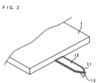
- Fig. 2 is a schematic perspective view showing the AFM probe.
- the needle-shaped body 13 protrudes from the end section of the cantilever 11 provided at one end of the probe holder 1.
- a metal coat 15 is formed on the rear face of the cantilever 11.
- the metal coat 15 is obtained by coating the rear face of the cantilever 11 with aluminum. In other words, the portion where the metal coat 15 is formed is located on the face different from the face on which the needle-shaped body 13 is provided.
- the aluminum constituting the metal coat 15 corresponds to a first metal.
- Figs. 3A, 3B and 3C are schematic views showing a method for manufacturing the probe 12 for tip-enhanced Raman scattering according to Embodiment 1.
- the cantilever 11 from the end section of which the needle-shaped body 13 protrudes, is dipped into an aqueous silver nitrate solution 3.
- the aqueous silver nitrate solution 3 is a solution containing Ag ions.
- the Ag ions contained in the aqueous silver nitrate solution 3 correspond to the ions of a second metal.
- a reducing agent for reducing metal ions is not contained in the aqueous silver nitrate solution 3.
- the cantilever 11 is dipped into the aqueous silver nitrate solution 3 so that the needle-shaped body 13 and at least part of the metal coat 15 formed on the rear face of the cantilever 11 are dipped into the aqueous silver nitrate solution 3. Furthermore, it is desirable that the cantilever 11 should be dipped into the aqueous silver nitrate solution 3 so that the tip end of the needle-shaped body 13 is directed upward. Ag is precipitated and Ag nanostructures are made to grow at the tip end of the needle-shaped body 13 by dipping the cantilever 11 into the aqueous silver nitrate solution 3.
- the Fermi level of the aluminum constituting the metal coat 15 is higher than the Fermi level of Si.
- the electrons inside the aluminum enter the Si constituting the cantilever 11.
- the electrons of the Si pass through the natural oxide film of the Si and flow out into the aqueous silver nitrate solution 3.
- the Ag ions in the aqueous silver nitrate solution 3 are reduced by the electrons having flowed out, and Ag nanostructures are precipitated. Since the electrons are most likely to flow out from the tip end of the needle-shaped body 13, the electrons of the Si mainly flow out from the tip end of the needle-shaped body 13 into the aqueous silver nitrate solution 3.
- the Ag nanostructures are precipitated and made to grow at the tip end of the needle-shaped body 13.
- the electrons are likely to flow out from the tip end of the needle-shaped body 13, and the Ag nanostructures are likely to be precipitated.
- the electrons are more likely to flow out, and the Ag nanostructures are more likely to be precipitated.
- the curvature of the tip end of the needle-shaped body 13 is larger, the electrons are more likely to flow out from the tip end of the needle-shaped body 13.
- the cantilever 11 After the cantilever 11 is dipped into the aqueous silver nitride solution 3 for an appropriate period of time, the cantilever 11 is taken out from the aqueous silver nitride solution 3 and washed. The washing, however, is not essential. As shown in Fig. 3B , the aggregate 14 of the Ag nanostructures is formed at the tip end of the needle-shaped body 13. In addition to the tip end of the needle-shaped body 13, the Ag nanostructures are also precipitated sometimes along the ridge lines of the cantilever 11 including the needle-shaped body 13.
- the size and shape of the aggregate 14 of the Ag nanostructures can be controlled, for example, by adjusting the concentration of the aqueous silver nitride solution 3 or the time during which the cantilever 11 is dipped into the aqueous silver nitride solution 3.
- the probe 12 for tip-enhanced Raman scattering in which the aggregate 14 of the Ag nanostructures is fixed to the tip end of the needle-shaped body 13 protruding from the cantilever 11 is manufactured as described above.
- Fig. 4 is a block diagram showing a configuration of a Raman scattering measurement apparatus.
- the Raman scattering measurement apparatus is equipped with a sample stand 5 on which a sample 2 is placed, the cantilever 11, the probe 12, an irradiation section 61 for applying laser light, and a lens 4 for converging the laser light from the irradiation section 61 to the tip end section of the probe 12 that is brought close to or made contact with the sample 2.
- the probe 12 is provided at the end section of the cantilever 11.
- the sample stand 5 has a sample placement face 51.
- the sample 2 can have any shape such as a flat plate, although the sample 2 having a granular shape is shown in Fig. 4 .
- the Raman scattering measurement apparatus is further equipped with a drive section 66 for moving the cantilever 11, a laser light source 67, an optical sensor 68, a signal processing section 69, and a control section 65.
- the drive section 66 brings the probe 12 close to the sample 2 placed on the sample placement face 51 by moving the cantilever 11.
- the laser light source 67 applies laser light to the rear face of the cantilever 11.
- the laser light is reflected by the metal coat 15 provided on the rear face of the cantilever 11.
- the optical sensor 68 detects the reflected laser light and outputs a signal indicating the result of the detection to the signal processing section 69.
- the laser light is indicated by dashed arrows.
- the cantilever 11 In the case that the tip end section of the probe 12 is brought close to or made contact with the sample 2, the cantilever 11 is bent by an atomic force, the position at which the laser light is detected by the optical sensor 68 is deviated, and the signal processing section 69 detects the bending of the cantilever 11.
- the change in the bending amount of the cantilever 11 corresponds to the change in the distance between the probe 12 and the surface of the sample 2.
- the signal processing section 69 controls the operation of the drive section 66 so that the bending of the cantilever 11 becomes constant.
- the control section 65 controls the operation of the signal processing section 69, thereby controlling the movement of the probe 12.
- the Raman scattering measurement apparatus may be configured to measure the current flowing between the probe 12 and the sample 2 and to control the movement of the probe 12 on the basis of the measured current.
- the Raman scattering measurement apparatus is further equipped with a beam splitter 62, a spectroscope 63, a detection section 64 for detecting light, and a drive section 50 for moving the sample stand 5 in the up-down direction or the left-right direction.
- the laser light applied by the irradiation section 61 passes through the beam splitter 62, is converged by the lens 4, and is applied to the tip end section of the probe 12 that is brought close to or made contact with the sample 2.
- the aggregate 14 of the Ag nanostructures formed at the tip end of the needle-shaped body 13 is included at the tip end section of the probe 12.
- the state of being brought close to is herein the state in which the aggregate 14 of the Ag nanostructures has approached the surface of the sample 2 to the distance to the extent that localized plasmons are induced on the surface of the sample 2 by the applied light, that a locally enhanced electric field is generated, and that tip-enhanced Raman scattering in which Raman scattering light is enhanced is generated.
- Tip-enhanced Raman scattering is generated at the portion on the sample 2 to which the tip end section of the probe 12 is brought close or with which the tip end section of the probe 12 is made contact and to which the laser light is applied.
- the generated Raman scattering light is condensed by the lens 4, is reflected by the beam splitter 62, and enters the spectroscope 63.
- the Raman scattering measurement apparatus is equipped with optical systems composed of numerous optical components, such as mirrors, lenses and filters, for guiding, condensing and separating the laser light and the Raman scattering light.
- optical systems other than the lens 4 and the beam splitter 62 are not shown.
- the spectroscope 63 disperses the incident Raman scattering light.
- the detection section 64 detects the light of various wavelengths dispersed by the spectroscope 63 and outputs signals corresponding to the detection intensity of the light of various wavelengths to the control section 65.
- the control section 65 controls the wavelengths of the light dispersed by the spectroscope 63 and the signals output from the detection section 64 are input to the control section 65, whereby the control section 65 generates a Raman spectrum on the basis of the wavelengths of the dispersed light and the detection intensity of the light indicated by the input signals. In this way, Tip-enhanced Raman scattering is measured.
- the control section 65 controls the operation of the drive section 50 to moves the sample stand 5, thereby making it possible to measure Tip-enhanced Raman scattering at various portions on the sample stand 5.
- the probe 12 in which the aggregate 14 of the Ag nanostructures is fixed to the tip end of the needle-shaped body 13 is manufactured by dipping the cantilever 11, from which the needle-shaped body 13 protrudes and on the rear face of which the metal coat 15 is formed, into the aqueous silver nitride solution 3. Since the Ag nanostructures are precipitated at the tip end of the needle-shaped body 13 by simply dipping the cantilever 11 into the aqueous silver nitride solution 3, the probe 12 for tip-enhanced Raman scattering can be manufactured with little labor without requiring large facilities for vacuum deposition.
- the size and shape of the aggregate 14 of the Ag nanostructures can be controlled by adjusting the concentration of the aqueous silver nitride solution 3 into which the cantilever 11 is dipped or by adjusting the dipping time.
- the size and shape of the aggregate 14 of the Ag nanostructures to be formed on the probe 12 can be controlled freely, whereby it is possible to form the aggregate 14 suited for the wavelengths of the laser light for Raman scattering.
- the probe 12 capable of obtaining the desired degree of enhancement at the time when tip-enhanced Raman scattering is measured can be manufactured by controlling the size and shape of the aggregate 14 of the Ag nanostructures.
- the entire face of the needle-shaped body 13 is not coated with Ag, and the aggregate 14 of the Ag nanostructures is concentratedly formed mainly at the tip end of the needle-shaped body 13.
- the first metal constituting the metal coat 15 may be metals other than aluminum, provided that the metals have Fermi levels higher than that of Si.
- the first metal may be chromium, iron, titanium, zirconium, magnesium, manganese, zinc, nickel, or tin.
- the cantilever 11 including the needle-shaped body 13 may be made of Si having a water resistant film such as a natural oxide film on the surface, or may partially contains Si having no water resistant film.
- the cantilever 11 may also be made of a semiconductor having a water resistant film such as a natural oxide film on the surface, other than Si.
- the first metal is a metal having a Fermi level higher than that of the semiconductor constituting the cantilever 11. What's more, the metal coat 15 made of the first metal may be formed at portions other than the rear face of the cantilever 11.
- the solution containing Ag ions may be solutions other than the aqueous silver nitride solution 3.
- the ions of the second metal contained in the solution into which the cantilever 11 is dipped may be the ions of metals other than Ag. Complex ions are included in the ions of the metal.
- the Fermi level of the solution containing the ions of the second metal or the chemical potential of the electrons in the solution containing the ions of the second metal is preferably lower than the Fermi level of the semiconductor constituting the cantilever 11.
- the Fermi levels referred to in this description respectively indicate Fermi levels before the semiconductor makes contact with a metal or a solution. What's more, although the Fermi level is a term used in semiconductor physics and the chemical potential of the electrons is a term used in solid-state physics and electrochemistry, the Fermi level of the solution containing the ions of the second metal is almost equivalent to the chemical potential of the electrons in the solution containing the ions of the second metal. Alternatively, the Fermi level of the second metal is preferably lower than the Fermi level of the semiconductor constituting the cantilever 11.
- the Fermi level of the solution containing the ions of the second metal should be lower than the Fermi level of the semiconductor constituting the cantilever 11 and that the Fermi level of the second metal should be lower than the Fermi level of the semiconductor constituting the cantilever 11.
- the second metal is, for example, Au (gold), platinum, iridium, palladium, copper or bismuth.
- solutions containing the ions of these metals are used, and the structures of these metals are formed at the tip end of the needle-shaped body 13.
- the probe 12 in which the aggregate of Au nanostructures precipitated at the tip end of the needle-shaped body 13 is manufactured using an aqueous potassium chloroaurate solution. Even in the case that the probe 12 in which the structures of Au, platinum, iridium, palladium, copper or bismuth are precipitated at the tip end of the needle-shaped body 13, tip-enhanced Raman scattering can be measured.
- the structure of the probe 12 is similar to that in Embodiment 1.
- the cantilever 11 is provided at one end of the probe holder 1, and the probe 12 is provided at the end section of the cantilever 11.
- the metal coat 15 is formed on the rear face of the cantilever 11.
- the probe 12 includes the needle-shaped body 13 protruding from the cantilever 11 and the aggregate 14 of metallic structures fixed to the tip end of the needle-shaped body 13.
- the metallic structures in this embodiment are Ag nanostructures.
- the first metal constituting the metal coat 15 is, for example, aluminum.
- the metal coat 15 desirably makes ohmic contact with the cantilever 11.
- the probe 12 is manufactured by dipping the cantilever 11 into a solution containing the ions of the second metal.
- the first metal constituting the metal coat 15 is a metal having an ionization tendency larger than that of the second metal.
- the Fermi level of the first metal in this embodiment may be not more than the Fermi level of the semiconductor constituting the cantilever 11 including the needle-shaped body 13. It is desirable that the cantilever 11 should be made of n-type Si and that the metal coat 15 should make ohmic contact with the cantilever 11.
- the second metal is Ag
- the first metal is aluminum
- the solution containing the ions of the second metal is the aqueous silver nitride solution 3.
- Aluminum has an ionization tendency larger than that of Ag.
- aluminum has a Fermi level lower than that of n-type Si.
- the Fermi level of the first metal is lower than the Fermi level of the semiconductor, the first metal makes Schottky contact with the semiconductor.
- the semiconductor is low-resistance highly doped n-type Si, the first metal makes ohmic contact with the semiconductor due to a quantum-mechanical tunneling phenomenon.
- an AFM probe in which a metal coat made of metal aluminum makes ohmic contact with the cantilever made of n-type Si having a resistance of 0.01 ⁇ cm is commercially available.
- the probe 12 is manufactured by dipping the cantilever 11 into the aqueous silver nitride solution 3.
- the cantilever 11 from the end section of which the needle-shaped body 13 protrudes, is dipped into the aqueous silver nitride solution 3.
- No reducing agent is contained in the aqueous silver nitrate solution 3.
- the cantilever 11 is dipped into the aqueous silver nitrate solution 3 so that the needle-shaped body 13 and at least part of the metal coat 15 are dipped into the aqueous silver nitrate solution 3.
- the ionization tendency of the aluminum constituting the metal coat 15 is larger than the ionization tendency of Ag.
- the aluminum inside the metal coat 15 tends to be oxidized, and the Ag ions inside the aqueous silver nitride solution 3 tend to be reduced.
- the Ag ions When aluminum is oxidized, electrons are emitted from the aluminum.
- the Ag ions When the Ag ions are reduced, the Ag ions absorb electrons. In other words, in the case that the cantilever 11 is dipped into the aqueous silver nitride solution 3, electrons flow from the aluminum inside the metal coat 15 to the Ag ions inside the aqueous silver nitride solution 3.
- the cantilever 11 Since negative carriers are contained in n-type Si, in the case that the cantilever 11 is made of n-type Si, electrons are likely to move inside the cantilever 11 including the needle-shaped body 13. Electrons are likely to flow out from the tip end of the needle-shaped body 13 into the aqueous silver nitride solution 3, and the Ag nanostructures are likely to be precipitated. Hence, the cantilever 11 is desirably made of an n-type semiconductor. What's more, as the curvature of the tip end of the needle-shaped body 13 is larger, electrons are more likely to flow out from the tip end of the needle-shaped body 13.
- the cantilever 11 After the cantilever 11 is dipped into the aqueous silver nitride solution 3 for an appropriate period of time, the cantilever 11 is taken out from the aqueous silver nitride solution 3 and washed. The washing, however, is not essential.
- the aggregate 14 of the Ag nanostructures is formed at the tip end of the needle-shaped body 13.
- the probe 12 in which the aggregate 14 of the Ag nanostructures is fixed to the tip end of the needle-shaped body 13 is manufactured.
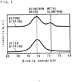
- Fig. 5 is a characteristic graph indicating the analysis result of XPS (X-ray Photoelectron Spectroscopy) for the metal coat 15.
- the horizontal axis represents binding energy
- the vertical axis represents the intensity of photoelectrons.
- the binding energy of aluminum oxide and the binding energy of metal aluminum are indicated by dotted lines.
- Fig. 5 shows the spectrum indicating the result of XPS conducted for the metal coat 15 before the dipping of the cantilever 11 into the aqueous silver nitride solution 3 and the spectrum indicating the result of XPS conducted for the metal coat 15 after the dipping of the cantilever 11 into the aqueous silver nitride solution 3.
- the configuration of the Raman scattering measurement apparatus equipped with the probe 12 is similar to that in Embodiment 1. Also in this embodiment, the Raman scattering measurement apparatus can measure tip-enhanced Raman scattering using the probe 12 in which the aggregate 14 of the Ag nanostructures is fixed to the tip end of the needle-shaped body 13.
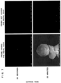
- Fig. 6 is a view showing actual examples of the probe 12.
- Fig. 6 shows a plurality of photographs obtained by photographing the tip ends of the needle-shaped bodies 13 of the probes 12 having been manufactured under a plurality of conditions.
- OMCL-AC160TS made by Olympus was used, and each probe 12 was manufactured by dipping the cantilever 11 into the aqueous silver nitride solution 3.
- the aqueous silver nitride solution 3 three kinds of solutions having silver nitrate concentrations of 0.05 mM, 0.1 mM and 1 mM were used. M herein represents mole/L.
- the dipping time during which the cantilever 11 was dipped in the aqueous silver nitride solution 3 was set to two kinds of values, 10 s and 60 s.
- Fig. 6 shows six photographs arranged in two lines and three rows.
- the respective two photographs in the left row, the intermediate row and the right row are photographs obtained by photographing the tip ends of the needle-shaped bodies 13 of the probes 12 having been manufactured at respective silver nitrate concentrations of 0.05 mM, 0.1 mM and 1 mM.
- the respective three photographs in the upper line and the lower line are photographs obtained by photographing the tip ends of the needle-shaped bodies 13 of the probes 12 having been manufactured at respective dipping time values of 10 s and 60 s.
- Each photograph shows the aggregate 14 of the Ag nanostructures. As the concentration of silver nitride is higher and as the dipping time is longer, the size of the aggregate 14 of the Ag nanostructures becomes larger.
- the aggregate 14 of the Ag nanostructures in the probe 12 having been manufactured at a silver nitrate concentration of 0.1 mM and at a dipping time value of 10 s had a size most suitable for measuring tip-enhanced Raman scattering.
- the probe 12 for tip-enhanced Raman scattering can be manufactured with little labor by dipping the cantilever 11, on the rear face of which the metal coat 15 is formed, into the aqueous silver nitride solution 3.
- the size and shape of the aggregate 14 of the Ag nanostructures to be formed on the probe 12 can be controlled freely by adjusting the concentration of the aqueous silver nitride solution 3 into which the cantilever 11 is dipped or by adjusting the dipping time, whereby it is possible to form the aggregate 14 suited for the wavelengths of the laser light for Raman scattering.
- the probe 12 capable of obtaining the desired degree of enhancement at the time when tip-enhanced Raman scattering is measured can be manufactured.
- the solution containing Ag ions may be solutions other than the aqueous silver nitride solution 3.
- the first metal constituting the metal coat 15 may be metals other than aluminum, provided that the ionization tendency of the first metal is larger than the ionization tendency of the second metal, and the ions of the second metal contained in the solution into which the cantilever 11 is dipped may be the ions of metals other than Ag.
- the first metal may be chromium, iron, titanium, zirconium, magnesium, manganese, zinc, nickel, or tin.
- the second metal may be Au (gold), platinum, iridium, palladium, copper, or bismuth.
- the metal coat 15 may be formed at portions other than the rear face of the cantilever 11, provided that the portions are other than the portion positioned at the tip end of the needle-shaped body 13.
- the Fermi level of the solution containing the ions of the second metal is lower than the Fermi level of the semiconductor constituting the cantilever 11 including the needle-shaped body 13. Since the Fermi level of the solution is lower than the Fermi level of the semiconductor, electrons are likely to flow out from the tip end of the needle-shaped body 13 to the solution, and the structures of the second metal are likely to be precipitated.
- the cantilever 11 may be made of semiconductors other than an n-type Si. In the case that the cantilever 11 is made of a p-type semiconductor, the metal coat 15 makes Schottky contact with the cantilever 11. Even in the case that the cantilever 11 is made of a p-type semiconductor or an intrinsic semiconductor, electrons move inside the semiconductor, and the structures of the second metal are precipitated at the tip end of the needle-shaped body 13, whereby the probe 12 is manufactured.
- the probe 12 is manufactured.
- the portion of the cantilever 11 covered with the metal coat 15 includes the tip end of the needle-shaped body 13.
- the ionization tendency of the first metal, such as aluminum, constituting the metal coat 15 is larger than the ionization tendency of the second metal, such as Ag.
- the probe 12 is manufactured.
- the ionization tendency of the first metal is larger than the ionization tendency of the second metal.
- electrons flow out from the cantilever 11 to the solution.
- electrons are likely to flow out from the tip end of the needle-shaped body 13, and as the curvature of the tip end of the needle-shaped body 13 is larger, electrons are more likely to flow out from the tip end of the needle-shaped body 13.
- the structures of the second metal are precipitated at the tip end of the needle-shaped body 13, whereby the probe 12 is manufactured.
- the metal coat 15 is not formed on the cantilever 11, and the probe 12 is provided at the end section of the cantilever 11.
- the probe 12 includes the needle-shaped body 13 protruding from the cantilever 11 and the aggregate 14 of metallic structures fixed to the tip end of the needle-shaped body 13.
- the cantilever 11 including the needle-shaped body 13 is made of an n-type Si.
- the metallic structures in this embodiment are Ag nanostructures.
- the probe 12 is manufactured by dipping the cantilever 11 into the aqueous silver nitride solution 3.
- the Fermi level of the aqueous silver nitride solution 3 is lower than the Fermi level of the n-type Si constituting the cantilever 11.
- the cantilever 11, from the end section of which the needle-shaped body 13 protrudes, is dipped into the aqueous silver nitride solution 3.
- No reducing agent is contained in the aqueous silver nitrate solution 3.
- the cantilever 11 is dipped into the aqueous silver nitride solution 3 so that the needle-shaped body 13 is dipped into the aqueous silver nitride solution 3.
- the cantilever 11 After the cantilever 11 is dipped into the aqueous silver nitride solution 3 for an appropriate period of time, the cantilever 11 is taken out from the aqueous silver nitride solution 3 and washed. The washing, however, is not essential.
- the aggregate 14 of the Ag nanostructures is formed at the tip end of the needle-shaped body 13.
- the probe 12 in which the aggregate 14 of the Ag nanostructures is fixed to the tip end of the needle-shaped body 13 is manufactured although the dipping time is required to be longer than in Embodiments 1 and 2.
- the Raman scattering measurement apparatus can measure tip-enhanced Raman scattering.
- Fig. 7 is a view showing actual examples of the probe 12 having the metal coat 15 formed on the cantilever 11 and the probe 12 not having the metal coat 15.
- Fig. 7 shows a plurality of photographs obtained by photographing the tip end of the probe 12 manufactured using the cantilever 11 having the metal coat 15 as in Embodiment 2, and by photographing the tip end of the probe 12 manufactured using the cantilever 11 not having the metal coat 15.
- the OMCL-AC160TS made by Olympus was used
- the OMCL-AC160TN made by Olympus was used as the probe holder 1 provided with the cantilever 11 not having the metal coat 15.
- the probes 12 were manufactured by dipping the cantilever 11 into the aqueous silver nitride solution 3.
- the silver nitrate concentration of the aqueous silver nitride solution 3 was set to 0.1 mM.
- the dipping time during which the cantilever 11 was dipped in the aqueous silver nitride solution was set to two kinds of values, 30 seconds and 30 minutes.
- Fig. 7 shows four photographs arranged in two lines and two rows.
- the two photographs in the left row are photographs obtained by photographing the tip ends of the needle-shaped bodies 13 of the probes 12 having been manufactured using the cantilevers 11 having the metal coat 15 formed thereon.
- the two photographs in the right row are photographs obtained by photographing the tip ends of the needle-shaped bodies 13 of the probes 12 having been manufactured using the cantilevers 11 not having the metal coat 15.
- the probes 12 shown in the photographs in the right row are the probes 12 manufactured by the manufacturing method according to this embodiment.
- the respective two photographs in the upper line and the lower line are photographs obtained by photographing the tip ends of the needle-shaped bodies 13 of the probes 12 having been manufactured at dipping time values of 30 seconds and 30 minutes, respectively.
- Each photograph shows the aggregate 14 of the Ag nanostructures.
- the size of the aggregate 14 of the Ag nanostructures is smaller even though the dipping time is the same.
- the aggregate 14 of the Ag nanostructures is made to grow further.
- the probe 12 containing the aggregate 14 of the Ag nanostructures having a sufficiently large size can be manufactured by making the dipping time sufficiently long.
- the probe 12 for tip-enhanced Raman scattering can be manufactured with little labor by dipping the cantilever 11 into the aqueous silver nitride solution 3.
- the size and shape of the aggregate 14 of the Ag nanostructures to be formed on the probe 12 can be controlled freely by adjusting the concentration of the aqueous silver nitride solution 3 into which the cantilever 11 is dipped or by adjusting the dipping time, whereby it is possible to form the aggregate 14 suited for the wavelengths of the laser light for Raman scattering.
- the probe 12 capable of obtaining the desired degree of enhancement at the time when tip-enhanced Raman scattering is measured can be manufactured.
- the solution containing Ag ions may be solutions other than the aqueous silver nitride solution 3.
- the ions of the second metal contained in the solution into which the cantilever 11 is dipped may be ions of metals other than Ag.
- the second metal may be Au (gold), platinum, iridium, palladium, copper, or bismuth.
- the Fermi level of the solution containing the ions of the second metal or the chemical potential of the electrons in the solution containing the ions of the second metal is preferably lower than the Fermi level of the semiconductor constituting the cantilever 11 including the needle-shaped body 13.
- the cantilever 11 may be made of semiconductors other than an n-type Si. Even in the case that the cantilever 11 is made of a p-type semiconductor or an intrinsic semiconductor, thermally excited electrons move inside the semiconductor, the structures of the second metal are precipitated at the tip end of the needle-shaped body 13, whereby the probe 12 is manufactured.
- Figs. 8A, 8B, 8C and 8D are schematic views showing a method for manufacturing the probe 12 according to Embodiment 4 which does not form part of the invention.
- the configuration of the probe 12 to be manufactured by the manufacturing method according to Embodiment 4 is similar to the configuration according to Embodiment 1, 2 or 3.
- the cantilever 11 similar to those according to Embodiments 1 to 3 is dipped into the aqueous silver nitride solution 3. Ag is precipitated at the tip end of the needle-shaped body 13 and the seed of the Ag nanostructures is formed.
- the cantilever 11 is pulled out from the aqueous silver nitride solution 3, and the needle-shaped body 13 is washed and dried as shown in Fig. 8B .
- the cantilever 11 is dipped into the aqueous silver nitride solution 3 again as shown in Fig. 8C .
- the Ag nanostructures are made to grow from the seed of the Ag nanostructures having been formed at the tip end of the needle-shaped body 13.
- the cantilever 11 is taken out from the aqueous silver nitride solution 3.
- the probe 12 for tip-enhanced Raman scattering in which the aggregate 14 of the Ag nanostructures is fixed to the tip end of the needle-shaped body 13 is manufactured as shown in Fig. 8D .
- the configuration of the Raman scattering measurement apparatus equipped with the probe 12 is similar to that in Embodiment 1.
- the probe 12 for tip-enhanced Raman scattering is manufactured by dipping the cantilever 11 into the aqueous silver nitride solution 3, by drying the needle-shaped body 13 once, and by dipping the cantilever 11 into the aqueous silver nitride solution 3 again.
- the aggregate 14 of the Ag nanostructures having a sharper or larger shape is obtained in some cases.
- the aggregate 14 of the Ag nanostructures can be made to grow further, and the probe 12 capable of obtaining the desired degree of enhancement at the time when tip-enhanced Raman scattering is measured can be manufactured.
- the solution containing Ag ions may be solutions other than the aqueous silver nitride solution 3.
- the ions of the second metal contained in the solution into which the cantilever 11 is dipped may be ions of metals other than Ag.
- the second metal may be Au (gold), platinum, iridium, palladium, copper, or bismuth.
- the solution into which the cantilever 11 is dipped first may be different from the solution into which the cantilever 11 is dipped again.
- a manufacturing kit for manufacturing the probe 12 can be used to execute the method for manufacturing the probes 12 according to Embodiments 1 to 4.
- the manufacturing kit includes the cantilever 11 and a solution such as the aqueous silver nitride solution 3 containing the ions of the second metal.
- the cantilever 11 included in the manufacturing kit is provided on the probe holder 1, and the metal coat 15 may be formed on the cantilever 11 or may not be formed.
- the solution included in the manufacturing kit may be used as the raw solution or may be diluted and used.
- the user can manufacture the probe 12 by dipping the cantilever 11 included in the manufacturing kit into the solution included in the manufacturing kit for an appropriate period of time.
- the cantilever 11 may not be included in the manufacturing kit.
- the user can manufacture the probe 12 using, for example, a commercially-available general-purpose cantilever 11 and the solution included in the manufacturing kit.
- the probe 12 having been manufactured by the manufacturing methods according to Embodiments 1 to 4 is used continuously to measure tip-enhanced Raman scattering
- the probe 12 is degraded by the deformation, oxidation or sulfurization of the aggregate 14 of metallic structures fixed to the tip end of the needle-shaped body 13.
- the probe 12 is also degraded in the case that substances other than the aggregate 14 of metallic structures adhere to the aggregate.
- the probe 12 is exposed to the atmosphere, the substances in the atmosphere are adsorbed by the aggregate 14 of metallic structures.
- the probe 12 is also degraded during its storage period.
- the enhancement of Raman scattering light becomes insufficient when tip-enhanced Raman scattering is measured.
- a reconditioned probe 12 is manufactured from a degraded probe 12.
- the probe 12 is reconditioned by removing part of the aggregate 14 of metallic structures from the degraded probe 12, by reducing the aggregate 14 of metallic structures or by removing substances adhered to aggregate 14 of metallic structures.
- the removal of part of the aggregate 14 of metallic structures and the removal of the adhered substances are executed by applying short-wavelength light, such as ultraviolet light, to the tip end of the needle-shaped body 13.
- short-wavelength light such as ultraviolet light
- Part of the aggregate 14 of metallic structures or the substances adhered to the aggregate 14 of metallic structures are removed from the needle-shaped body 13 by applying the short-wavelength light.
- a stripping solution is used to remove part of the aggregate 14 of metallic structures and to remove the adhered substances.
- Part of the aggregate 14 of metallic structures and the substances adhered to the aggregate 14 of metallic structures are removed from the probe 12 by dipping the probe 12 into a stripping solution, such as hydrochloric acid, sulfuric acid, nitric acid, acetic acid, thio nitric acid, etc.
- the degraded probe is reconditioned by removing degraded part of the aggregate 14 of metallic structures.
- the degraded probe is reconditioned by removing the substances adhered to the aggregate 14 of metallic structures.
- a reconditioned probe 12 is manufactured.
- the reconditioned probe 12 may be manufactured by executing any one of the manufacturing methods according to Embodiments 1 to 4 using the cantilever 11 from which part or whole of the aggregate 14 of metallic structures has been removed from the needle-shaped body 13.
- the reduction of the aggregate 14 of the metallic structures is performed by heating or a method in which a reducing agent is used.
- Part of the aggregate 14 of metallic structures is reduced by dipping the probe 12 into a solution in which a reducing agent, such as NaBH 4 , is used as a solute.
- the degraded probe 12 is reconditioned by reducing oxidized part of the aggregate 14 of metallic structures. In this way, the reconditioned probe 12 is manufactured.
- the measurement of tip-enhanced Raman scattering can be made using the manufactured probe 12.
- the probe 12 can be reconditioned so that the desired degree of enhancement is obtained at the time when tip-enhanced Raman scattering is measured.
- the cantilever 11 can be recycled.
- the manufacturing kit for manufacturing the probe 12 can be used to execute the method for manufacturing the probe 12 according to the embodiment.
- the manufacturing kit includes the cantilever 11, a solution such as the aqueous silver nitride solution 3 containing the ions of the second metal, and a reconditioning liquid for reconditioning the probe 12.
- the metal coat 15 may be formed on the cantilever 11, or may not be formed.
- the reconditioning liquid is a stripping solution, such as hydrochloric acid, sulfuric acid, nitric acid, acetic acid, thio nitric acid, etc. or a solution in which a reducing agent, such as NaBH 4 , is used as a solute.
- Each of the solution and the reconditioning liquid included in the manufacturing kit may be used as the raw solution or may be diluted and used.
- the user can manufacture the probe 12 by dipping the cantilever 11 included in the manufacturing kit into the solution included in the manufacturing kit. Furthermore, the user can manufacture a reconditioned probe 12 by dipping a used probe 12 into the reconditioning liquid for an appropriate period of time.
- the cantilever 11 may not be included in the manufacturing kit.
- the solution containing the ions of the second metal is an aqueous solution in Embodiments 1 to 5 described above
- the solution containing the ions of the second metal into which the cantilever 11 is to be dipped may be a solution in which a solvent other than water, such as an organic solvent, is used.
Description
- The present invention relates to a probe for measuring tip-enhanced Raman scattering and to a probe manufacturing method.
- Tip-enhanced Raman scattering is a method in which the metal-made tip end of a probe is brought close to or made contact with a sample, light is applied to the tip end of the probe, and enhanced Raman scattering light is made to be generated from the sample. Localized plasmons are induced by applying light to the metal-made tip end of the probe, a locally enhanced electric field is generated, and Raman scattering light is enhanced. Raman spectroscopic analysis for a minute area of the sample is made possible by tip-enhanced Raman scattering.
- A metal probe for STM (Scanning Tunneling Microscope) or a probe obtained by depositing a metal on a probe for AFM (Atomic Force Microscope) has been used conventionally as the probe.
Japanese Patent Application Laid-Open Publication No. 2009-156602 -
US 2006/0043276 A1 describes a method for manufacturing a probe for a near-field microscope, wherein a cantilever made of silicon and having a probe whose shape is a quadrangular pyramid is immersed in a silver nitrate aqueous solution so that the whole cantilever is covered with silver crystals. In a similar method which is disclosed in WANG J ET AL: "Controllable method for the preparation of metallized probes for efficient scanning near-field optical Raman microscopy", APPLIED PHYSICS LETTERS, A I P PUBLISHING LLC, US, vol. 86, no. 26, 23 June 2005 (2005-06-23), pages 263111-263111, ISSN: 0003-6951, DOI: 10.1063/1.1978983, a cantilever made of silicon from which a needle-shaped body protrudes is dipped into a solution containing silver ions. According to the method a probe is manufactured in which silver structures are precipitated at a tip end of the needle-shaped body. - Further examples of methods for manufacturing a probe are disclosed in
US 6 002 471 A , Przemyslaw R. Brejna et al: "Electroless Deposition of Silver onto Silicon as a Method of Preparation of Reproducible Surface-Enhanced Raman Spectroscopy Substrates and Tip-Enhanced Raman Spectroscopy Tips" (APPLIED SPECTROSCOPY., vol. 64, no. 5, 1 May 2010 (2010-05-01), pages 493-499, XP055556911, US ISSN: 0003-7028, DOI: 10.1366/000370210791211682) - The enhancement degree of Raman scattering light due to tip-enhanced Raman scattering depends on the sizes and shapes of metallic nanostructures formed at the tip end of a probe. In the case of the conventional metal vapor deposition method, since the probe is entirely coated with a metal, it is difficult to make the sizes and shapes of the metal nanostructures formed at the tip end of the probe to the sizes and shapes suited for the wavelengths of various kinds of excitation light for Raman spectroscopy. Furthermore, the conventional method has a problem of requiring large facilities, such as a vacuum chamber and a vacuum pump, to perform metal vapor deposition.
- The present disclosure is made in consideration of the above-mentioned circumstances, and objects of the present disclosure is to provide a probe manufacturing method capable of simplifying the manufacturing of a probe and capable of properly controlling the sizes and shapes of metal nanostructures and to provide a probe.
- The present invention provides a method for manufacturing a probe protruding from a cantilever with the features of
claim 1 and a method for manufacturing a probe protruding from a cantilever with the features of claim 2. - When the method according to
claim 1 is performed, the cantilever, part of which is coated with the first metal having a Fermi level higher than that of the semiconductor serving as the material thereof, is dipped into the solution containing the ions of the second metal. The needle-shaped body protrudes from the cantilever. The electrons of the semiconductor effectively flow out to the solution due to the presence of the first metal, and the structures of the second metal are precipitated at the tip end of the needle-shaped body. The probe for tip-enhanced Raman scattering in which the metal structures are fixed to the tip end of the needle-shaped body is manufactured. - When the method according to claim 2 is performed, since the ionization tendency of the first metal is larger than the ionization tendency of the second metal, the first metal tends to be oxidized, and the ions of the second metal tend to be reduced. When the first metal is oxidized, electrons flow from the metal coat to the cantilever, electrons flow out from the tip end of the needle-shaped body to the solution, and the ions of the second metal are reduced. Hence, the structures of the second metal are precipitated at the tip end of the needle-shaped body.
- In the method for manufacturing the probe according to an aspect of the present invention, the first metal is aluminum, chromium, iron, titanium, zirconium, magnesium, manganese, zinc, nickel, or tin.
- If the first metal is aluminum, chromium, iron, titanium, zirconium, magnesium, manganese, zinc, nickel, or tin, electrons are supplied from the metal coat to the needle-shaped body in the case that part of the cantilever is coated with the metal coat made of these metals.
- In the method for manufacturing the probe according to an aspect of the present invention, after the cantilever is dipped into the solution, the dipping is interrupted, the needle-shaped body is dried, and the cantilever is dipped into the solution again.
- Then, after the cantilever is dipped into the solution, the needle-shaped body is dried once, and the cantilever is dipped into the solution again. The seed of the metal structures is formed by the first dipping, and the metal structures are made to grow further by the second dipping.
- In the method for manufacturing the probe according to an aspect of the present invention, the solution is a solution containing ions of silver, gold, platinum, iridium, palladium, copper or bismuth.
- If the solution contains the ions of silver, gold, platinum, iridium, palladium, copper or bismuth, the metal structures of silver, gold, platinum, iridium, palladium, copper or bismuth are precipitated at the tip end of the needle-shaped body. Tip-enhanced Raman scattering can be measured using the probe containing these metal structures.
- The method for manufacturing the probe according to an aspect of the present inventon is characterized by further comprising the step of: removing part of the structures contained in a degraded probe, reducing the structures or removing substances adhered to the structures.
- Then, the probe is reconditioned by removing degraded part of the metal structures contained in the degraded probe or by reducing the degraded part.
-
-
Fig. 1 is a schematic view showing a probe for tip-enhanced Raman scattering; -
Fig. 2 is a schematic perspective view showing an AFM probe; -
Fig. 3A is a schematic view showing a method for manufacturing a probe for tip-enhanced Raman scattering according toEmbodiment 1; -
Fig. 3B is a schematic view showing a method for manufacturing a probe for tip-enhanced Raman scattering according toEmbodiment 1; -
Fig. 3C is a schematic view showing a method for manufacturing a probe for tip-enhanced Raman scattering according toEmbodiment 1; -
Fig. 4 is a block diagram showing a configuration of a Raman scattering measurement apparatus; -
Fig. 5 is a characteristic graph indicating the analysis result of XPS for a metal coat; -
Fig. 6 is a view showing actual examples of the probe; -
Fig. 7 is a view showing actual examples of the probe having the metal coat formed on a cantilever and the probe not having the metal coat; -
Fig. 8A is a schematic view showing a method for manufacturing a probe according toEmbodiment 4; -
Fig. 8B is a schematic view showing a method for manufacturing the probe according toEmbodiment 4; -
Fig. 8C is a schematic view showing a method for manufacturing the probe according toEmbodiment 4; and -
Fig. 8D is a schematic view showing a method for manufacturing the probe according toEmbodiment 4.Embodiments - The present invention will be described specifically on the basis of the drawings showing embodiments thereof.
-
Fig. 1 is a schematic view showing a probe for tip-enhanced Raman scattering. Aprobe holder 1 is made of Si (silicon) and is formed in a flat plate shape. Acantilever 11 is provided at one end of theprobe holder 1. Thecantilever 11 is shown enlarged in the figure. Aprobe 12 is provided at the end section of thecantilever 11. Furthermore, the tip end portion of theprobe 12 is shown enlarged in the figure. Theprobe 12 includes a needle-shapedbody 13 protruding from thecantilever 11 and anaggregate 14 of metallic structures fixed to the tip end of the needle-shapedbody 13. Thecantilever 11 has two faces having a front-rear relationship, and the needle-shapedbody 13 protrudes from one face of thecantilever 11. The other face of thecantilever 11, that is, the face on the opposite side of the face that is provided with theprobe 12, is hereafter referred to as the rear face. Moreover, thecantilever 11 is assumed to include the needle-shapedbody 13. The needle-shapedbody 13 is made of Si, has a pyramid shape and is integrated with thecantilever 11 by Si. For example, thecantilever 11 including the needle-shapedbody 13 is formed of a single crystal of Si. Theaggregate 14 of metallic structures is formed by aggregating a plurality of metallic structures. This embodiment shows an example in which the metallic structures are Ag nanostructures formed of nano-sized Ag (silver). The size of each of the Ag nanostructures is a few nm or more and less than 1 µm, and the size of theaggregate 14 of the Ag nanostructures is a few µm or less. - The
probe 12 for tip-enhanced Raman scattering is manufactured from an AFM probe.Fig. 2 is a schematic perspective view showing the AFM probe. The needle-shapedbody 13 protrudes from the end section of thecantilever 11 provided at one end of theprobe holder 1. Furthermore, ametal coat 15 is formed on the rear face of thecantilever 11. Themetal coat 15 is obtained by coating the rear face of thecantilever 11 with aluminum. In other words, the portion where themetal coat 15 is formed is located on the face different from the face on which the needle-shapedbody 13 is provided. The aluminum constituting themetal coat 15 corresponds to a first metal. -
Figs. 3A, 3B and 3C are schematic views showing a method for manufacturing theprobe 12 for tip-enhanced Raman scattering according toEmbodiment 1. As shown inFig. 3A , thecantilever 11, from the end section of which the needle-shapedbody 13 protrudes, is dipped into an aqueoussilver nitrate solution 3. The aqueoussilver nitrate solution 3 is a solution containing Ag ions. The Ag ions contained in the aqueoussilver nitrate solution 3 correspond to the ions of a second metal. A reducing agent for reducing metal ions is not contained in the aqueoussilver nitrate solution 3. At this time, thecantilever 11 is dipped into the aqueoussilver nitrate solution 3 so that the needle-shapedbody 13 and at least part of themetal coat 15 formed on the rear face of thecantilever 11 are dipped into the aqueoussilver nitrate solution 3. Furthermore, it is desirable that thecantilever 11 should be dipped into the aqueoussilver nitrate solution 3 so that the tip end of the needle-shapedbody 13 is directed upward. Ag is precipitated and Ag nanostructures are made to grow at the tip end of the needle-shapedbody 13 by dipping thecantilever 11 into the aqueoussilver nitrate solution 3. - The Fermi level of the aluminum constituting the
metal coat 15 is higher than the Fermi level of Si. The electrons inside the aluminum enter the Si constituting thecantilever 11. As the electrons enter from the aluminum, the electrons of the Si pass through the natural oxide film of the Si and flow out into the aqueoussilver nitrate solution 3. The Ag ions in the aqueoussilver nitrate solution 3 are reduced by the electrons having flowed out, and Ag nanostructures are precipitated. Since the electrons are most likely to flow out from the tip end of the needle-shapedbody 13, the electrons of the Si mainly flow out from the tip end of the needle-shapedbody 13 into the aqueoussilver nitrate solution 3. Hence, the Ag nanostructures are precipitated and made to grow at the tip end of the needle-shapedbody 13. As the natural oxide film of the Si is thinner, the electrons are likely to flow out from the tip end of the needle-shapedbody 13, and the Ag nanostructures are likely to be precipitated. Ideally, in the state in which the natural oxide film of Si does not exist, the electrons are more likely to flow out, and the Ag nanostructures are more likely to be precipitated. Moreover, as the curvature of the tip end of the needle-shapedbody 13 is larger, the electrons are more likely to flow out from the tip end of the needle-shapedbody 13. - After the
cantilever 11 is dipped into the aqueoussilver nitride solution 3 for an appropriate period of time, thecantilever 11 is taken out from the aqueoussilver nitride solution 3 and washed. The washing, however, is not essential. As shown inFig. 3B , theaggregate 14 of the Ag nanostructures is formed at the tip end of the needle-shapedbody 13. In addition to the tip end of the needle-shapedbody 13, the Ag nanostructures are also precipitated sometimes along the ridge lines of thecantilever 11 including the needle-shapedbody 13. The size and shape of theaggregate 14 of the Ag nanostructures can be controlled, for example, by adjusting the concentration of the aqueoussilver nitride solution 3 or the time during which thecantilever 11 is dipped into the aqueoussilver nitride solution 3. As shown inFigs. 3B and 3C , theprobe 12 for tip-enhanced Raman scattering in which theaggregate 14 of the Ag nanostructures is fixed to the tip end of the needle-shapedbody 13 protruding from thecantilever 11 is manufactured as described above. -
Fig. 4 is a block diagram showing a configuration of a Raman scattering measurement apparatus. The Raman scattering measurement apparatus is equipped with a sample stand 5 on which a sample 2 is placed, thecantilever 11, theprobe 12, an irradiation section 61 for applying laser light, and alens 4 for converging the laser light from the irradiation section 61 to the tip end section of theprobe 12 that is brought close to or made contact with the sample 2. Theprobe 12 is provided at the end section of thecantilever 11. The sample stand 5 has asample placement face 51. Furthermore, the sample 2 can have any shape such as a flat plate, although the sample 2 having a granular shape is shown inFig. 4 . - The Raman scattering measurement apparatus is further equipped with a
drive section 66 for moving thecantilever 11, alaser light source 67, anoptical sensor 68, asignal processing section 69, and acontrol section 65. Thedrive section 66 brings theprobe 12 close to the sample 2 placed on thesample placement face 51 by moving thecantilever 11. Thelaser light source 67 applies laser light to the rear face of thecantilever 11. The laser light is reflected by themetal coat 15 provided on the rear face of thecantilever 11. Theoptical sensor 68 detects the reflected laser light and outputs a signal indicating the result of the detection to thesignal processing section 69. InFig. 4 , the laser light is indicated by dashed arrows. In the case that the tip end section of theprobe 12 is brought close to or made contact with the sample 2, thecantilever 11 is bent by an atomic force, the position at which the laser light is detected by theoptical sensor 68 is deviated, and thesignal processing section 69 detects the bending of thecantilever 11. The change in the bending amount of thecantilever 11 corresponds to the change in the distance between theprobe 12 and the surface of the sample 2. Thesignal processing section 69 controls the operation of thedrive section 66 so that the bending of thecantilever 11 becomes constant. Thecontrol section 65 controls the operation of thesignal processing section 69, thereby controlling the movement of theprobe 12. The Raman scattering measurement apparatus may be configured to measure the current flowing between theprobe 12 and the sample 2 and to control the movement of theprobe 12 on the basis of the measured current. - The Raman scattering measurement apparatus is further equipped with a
beam splitter 62, aspectroscope 63, adetection section 64 for detecting light, and adrive section 50 for moving the sample stand 5 in the up-down direction or the left-right direction. The laser light applied by the irradiation section 61 passes through thebeam splitter 62, is converged by thelens 4, and is applied to the tip end section of theprobe 12 that is brought close to or made contact with the sample 2. Theaggregate 14 of the Ag nanostructures formed at the tip end of the needle-shapedbody 13 is included at the tip end section of theprobe 12. The state of being brought close to is herein the state in which theaggregate 14 of the Ag nanostructures has approached the surface of the sample 2 to the distance to the extent that localized plasmons are induced on the surface of the sample 2 by the applied light, that a locally enhanced electric field is generated, and that tip-enhanced Raman scattering in which Raman scattering light is enhanced is generated. Tip-enhanced Raman scattering is generated at the portion on the sample 2 to which the tip end section of theprobe 12 is brought close or with which the tip end section of theprobe 12 is made contact and to which the laser light is applied. The generated Raman scattering light is condensed by thelens 4, is reflected by thebeam splitter 62, and enters thespectroscope 63. InFig. 4 , the laser light applied to the sample 2 and the Raman scattering light are indicated by solid arrows. The Raman scattering measurement apparatus is equipped with optical systems composed of numerous optical components, such as mirrors, lenses and filters, for guiding, condensing and separating the laser light and the Raman scattering light. InFig. 4 , optical systems other than thelens 4 and thebeam splitter 62 are not shown. Thespectroscope 63 disperses the incident Raman scattering light. Thedetection section 64 detects the light of various wavelengths dispersed by thespectroscope 63 and outputs signals corresponding to the detection intensity of the light of various wavelengths to thecontrol section 65. Thecontrol section 65 controls the wavelengths of the light dispersed by thespectroscope 63 and the signals output from thedetection section 64 are input to thecontrol section 65, whereby thecontrol section 65 generates a Raman spectrum on the basis of the wavelengths of the dispersed light and the detection intensity of the light indicated by the input signals. In this way, Tip-enhanced Raman scattering is measured. Thecontrol section 65 controls the operation of thedrive section 50 to moves the sample stand 5, thereby making it possible to measure Tip-enhanced Raman scattering at various portions on the sample stand 5. - As described above in detail, with this embodiment, the
probe 12 in which theaggregate 14 of the Ag nanostructures is fixed to the tip end of the needle-shapedbody 13 is manufactured by dipping thecantilever 11, from which the needle-shapedbody 13 protrudes and on the rear face of which themetal coat 15 is formed, into the aqueoussilver nitride solution 3. Since the Ag nanostructures are precipitated at the tip end of the needle-shapedbody 13 by simply dipping thecantilever 11 into the aqueoussilver nitride solution 3, theprobe 12 for tip-enhanced Raman scattering can be manufactured with little labor without requiring large facilities for vacuum deposition. The size and shape of theaggregate 14 of the Ag nanostructures can be controlled by adjusting the concentration of the aqueoussilver nitride solution 3 into which thecantilever 11 is dipped or by adjusting the dipping time. Hence, the size and shape of theaggregate 14 of the Ag nanostructures to be formed on theprobe 12 can be controlled freely, whereby it is possible to form the aggregate 14 suited for the wavelengths of the laser light for Raman scattering. As a result, when tip-enhanced Raman scattering is measured using theprobe 12, effective enhancement of Raman scattering light is made possible. Furthermore, theprobe 12 capable of obtaining the desired degree of enhancement at the time when tip-enhanced Raman scattering is measured can be manufactured by controlling the size and shape of theaggregate 14 of the Ag nanostructures. - Moreover, since according to the invention a reducing agent for reducing metal ions is not contained in the aqueous
silver nitride solution 3, the entire face of the needle-shapedbody 13 is not coated with Ag, and theaggregate 14 of the Ag nanostructures is concentratedly formed mainly at the tip end of the needle-shapedbody 13. - Although the example in which the
metal coat 15 formed on thecantilever 11 is made of aluminum is described in this embodiment, the first metal constituting themetal coat 15 may be metals other than aluminum, provided that the metals have Fermi levels higher than that of Si. For example, the first metal may be chromium, iron, titanium, zirconium, magnesium, manganese, zinc, nickel, or tin. Furthermore, thecantilever 11 including the needle-shapedbody 13 may be made of Si having a water resistant film such as a natural oxide film on the surface, or may partially contains Si having no water resistant film. Moreover, thecantilever 11 may also be made of a semiconductor having a water resistant film such as a natural oxide film on the surface, other than Si. In this case, the first metal is a metal having a Fermi level higher than that of the semiconductor constituting thecantilever 11. What's more, themetal coat 15 made of the first metal may be formed at portions other than the rear face of thecantilever 11. - Furthermore, although the mode in which the
cantilever 11 is dipped into the aqueoussilver nitride solution 3 has been described in this embodiment, the solution containing Ag ions may be solutions other than the aqueoussilver nitride solution 3. Moreover, the ions of the second metal contained in the solution into which thecantilever 11 is dipped may be the ions of metals other than Ag. Complex ions are included in the ions of the metal. The Fermi level of the solution containing the ions of the second metal or the chemical potential of the electrons in the solution containing the ions of the second metal is preferably lower than the Fermi level of the semiconductor constituting thecantilever 11. The Fermi levels referred to in this description respectively indicate Fermi levels before the semiconductor makes contact with a metal or a solution. What's more, although the Fermi level is a term used in semiconductor physics and the chemical potential of the electrons is a term used in solid-state physics and electrochemistry, the Fermi level of the solution containing the ions of the second metal is almost equivalent to the chemical potential of the electrons in the solution containing the ions of the second metal. Alternatively, the Fermi level of the second metal is preferably lower than the Fermi level of the semiconductor constituting thecantilever 11. According toEmbodiment 1 of the invention, the Fermi level of the solution containing the ions of the second metal (or the chemical potential of the electrons) should be lower than the Fermi level of the semiconductor constituting thecantilever 11 and that the Fermi level of the second metal should be lower than the Fermi level of the semiconductor constituting thecantilever 11. - The second metal is, for example, Au (gold), platinum, iridium, palladium, copper or bismuth. In this embodiment, solutions containing the ions of these metals are used, and the structures of these metals are formed at the tip end of the needle-shaped
body 13. For example, theprobe 12 in which the aggregate of Au nanostructures precipitated at the tip end of the needle-shapedbody 13 is manufactured using an aqueous potassium chloroaurate solution. Even in the case that theprobe 12 in which the structures of Au, platinum, iridium, palladium, copper or bismuth are precipitated at the tip end of the needle-shapedbody 13, tip-enhanced Raman scattering can be measured. - In Embodiment 2, the structure of the
probe 12 is similar to that inEmbodiment 1. As inEmbodiment 1, thecantilever 11 is provided at one end of theprobe holder 1, and theprobe 12 is provided at the end section of thecantilever 11. Themetal coat 15 is formed on the rear face of thecantilever 11. Theprobe 12 includes the needle-shapedbody 13 protruding from thecantilever 11 and theaggregate 14 of metallic structures fixed to the tip end of the needle-shapedbody 13. The metallic structures in this embodiment are Ag nanostructures. The first metal constituting themetal coat 15 is, for example, aluminum. Themetal coat 15 desirably makes ohmic contact with thecantilever 11. - The
probe 12 is manufactured by dipping thecantilever 11 into a solution containing the ions of the second metal. In Embodiment 2, the first metal constituting themetal coat 15 is a metal having an ionization tendency larger than that of the second metal. The Fermi level of the first metal in this embodiment may be not more than the Fermi level of the semiconductor constituting thecantilever 11 including the needle-shapedbody 13. It is desirable that thecantilever 11 should be made of n-type Si and that themetal coat 15 should make ohmic contact with thecantilever 11. For example, the second metal is Ag, the first metal is aluminum, and the solution containing the ions of the second metal is the aqueoussilver nitride solution 3. Aluminum has an ionization tendency larger than that of Ag. Furthermore, aluminum has a Fermi level lower than that of n-type Si. In the case that the Fermi level of the first metal is lower than the Fermi level of the semiconductor, the first metal makes Schottky contact with the semiconductor. However, in the case that the semiconductor is low-resistance highly doped n-type Si, the first metal makes ohmic contact with the semiconductor due to a quantum-mechanical tunneling phenomenon. For example, an AFM probe in which a metal coat made of metal aluminum makes ohmic contact with the cantilever made of n-type Si having a resistance of 0.01 Ωcm is commercially available. - Also in this embodiment, as in
Embodiment 1, theprobe 12 is manufactured by dipping thecantilever 11 into the aqueoussilver nitride solution 3. As shown inFig. 3A , thecantilever 11, from the end section of which the needle-shapedbody 13 protrudes, is dipped into the aqueoussilver nitride solution 3. No reducing agent is contained in the aqueoussilver nitrate solution 3. Thecantilever 11 is dipped into the aqueoussilver nitrate solution 3 so that the needle-shapedbody 13 and at least part of themetal coat 15 are dipped into the aqueoussilver nitrate solution 3. - The ionization tendency of the aluminum constituting the
metal coat 15 is larger than the ionization tendency of Ag. Hence, the aluminum inside themetal coat 15 tends to be oxidized, and the Ag ions inside the aqueoussilver nitride solution 3 tend to be reduced. When aluminum is oxidized, electrons are emitted from the aluminum. When the Ag ions are reduced, the Ag ions absorb electrons. In other words, in the case that thecantilever 11 is dipped into the aqueoussilver nitride solution 3, electrons flow from the aluminum inside themetal coat 15 to the Ag ions inside the aqueoussilver nitride solution 3. In the state in which themetal coat 15 makes ohmic contact with thecantilever 11, electrons are likely to flow from themetal coat 15 to thecantilever 11. Even in the case that the Fermi level of the first metal (aluminum) is not more than the Fermi level of the semiconductor (n-type Si) constituting thecantilever 11, electrons flow from themetal coat 15 to thecantilever 11 by the ohmic contact. Hence, the aluminum inside themetal coat 15 is oxidized, and electrons flow from themetal coat 15 to thecantilever 11. Moreover, electrons are most likely to flow out from the tip end of the needle-shapedbody 13. As a result, electrons flow from themetal coat 15 to thecantilever 11, whereby electrons are supplied to the needle-shapedbody 13 and electrons flow from the tip end of the needle-shapedbody 13 into the aqueoussilver nitride solution 3. The Ag ions inside the aqueoussilver nitride solution 3 are reduced by the electrons having flown out. Consequently, the Ag nanostructures are precipitated and made to grow at the tip end of the needle-shapedbody 13. - Since negative carriers are contained in n-type Si, in the case that the
cantilever 11 is made of n-type Si, electrons are likely to move inside thecantilever 11 including the needle-shapedbody 13. Electrons are likely to flow out from the tip end of the needle-shapedbody 13 into the aqueoussilver nitride solution 3, and the Ag nanostructures are likely to be precipitated. Hence, thecantilever 11 is desirably made of an n-type semiconductor. What's more, as the curvature of the tip end of the needle-shapedbody 13 is larger, electrons are more likely to flow out from the tip end of the needle-shapedbody 13. - After the
cantilever 11 is dipped into the aqueoussilver nitride solution 3 for an appropriate period of time, thecantilever 11 is taken out from the aqueoussilver nitride solution 3 and washed. The washing, however, is not essential. As shown inFig. 3B , theaggregate 14 of the Ag nanostructures is formed at the tip end of the needle-shapedbody 13. As shown inFigs. 3B and 3C , theprobe 12 in which theaggregate 14 of the Ag nanostructures is fixed to the tip end of the needle-shapedbody 13 is manufactured. -
Fig. 5 is a characteristic graph indicating the analysis result of XPS (X-ray Photoelectron Spectroscopy) for themetal coat 15. The horizontal axis represents binding energy, and the vertical axis represents the intensity of photoelectrons. Furthermore, the binding energy of aluminum oxide and the binding energy of metal aluminum are indicated by dotted lines.Fig. 5 shows the spectrum indicating the result of XPS conducted for themetal coat 15 before the dipping of thecantilever 11 into the aqueoussilver nitride solution 3 and the spectrum indicating the result of XPS conducted for themetal coat 15 after the dipping of thecantilever 11 into the aqueoussilver nitride solution 3. According to the comparison between the spectra before and after the dipping, the peak intensity of the metal aluminum decreases, and the peak intensity of the aluminum oxide increases. It is obvious that the oxidation of the aluminum inside themetal coat 15 proceeded by dipping thecantilever 11 into the aqueoussilver nitride solution 3. Hence, it is assumed that the aluminum was oxidized due to the difference between the ionization tendencies of the aluminum (first metal) and the silver (second metal), that electrons flowed from the aluminum to the aqueoussilver nitride solution 3 via the n-type Si constituting thecantilever 11, and that the ions of silver were reduced, whereby the Ag nanostructures were precipitated. This reaction is assumed to be represented by the following chemical reaction formula.
Al+3AgNO3+3H2O → Al(OH)3+3Ag+3HNO3
- The configuration of the Raman scattering measurement apparatus equipped with the
probe 12 is similar to that inEmbodiment 1. Also in this embodiment, the Raman scattering measurement apparatus can measure tip-enhanced Raman scattering using theprobe 12 in which theaggregate 14 of the Ag nanostructures is fixed to the tip end of the needle-shapedbody 13. -
Fig. 6 is a view showing actual examples of theprobe 12.Fig. 6 shows a plurality of photographs obtained by photographing the tip ends of the needle-shapedbodies 13 of theprobes 12 having been manufactured under a plurality of conditions. As theprobe holder 1 provided with thecantilever 11, OMCL-AC160TS made by Olympus was used, and eachprobe 12 was manufactured by dipping thecantilever 11 into the aqueoussilver nitride solution 3. As the aqueoussilver nitride solution 3, three kinds of solutions having silver nitrate concentrations of 0.05 mM, 0.1 mM and 1 mM were used. M herein represents mole/L. Furthermore, the dipping time during which thecantilever 11 was dipped in the aqueoussilver nitride solution 3 was set to two kinds of values, 10 s and 60 s. -
Fig. 6 shows six photographs arranged in two lines and three rows. The respective two photographs in the left row, the intermediate row and the right row are photographs obtained by photographing the tip ends of the needle-shapedbodies 13 of theprobes 12 having been manufactured at respective silver nitrate concentrations of 0.05 mM, 0.1 mM and 1 mM. Furthermore, the respective three photographs in the upper line and the lower line are photographs obtained by photographing the tip ends of the needle-shapedbodies 13 of theprobes 12 having been manufactured at respective dipping time values of 10 s and 60 s. Each photograph shows theaggregate 14 of the Ag nanostructures. As the concentration of silver nitride is higher and as the dipping time is longer, the size of theaggregate 14 of the Ag nanostructures becomes larger. Of the sixprobes 12 shown inFig. 6 , theaggregate 14 of the Ag nanostructures in theprobe 12 having been manufactured at a silver nitrate concentration of 0.1 mM and at a dipping time value of 10 s had a size most suitable for measuring tip-enhanced Raman scattering. - Also in this embodiment, the
probe 12 for tip-enhanced Raman scattering can be manufactured with little labor by dipping thecantilever 11, on the rear face of which themetal coat 15 is formed, into the aqueoussilver nitride solution 3. The size and shape of theaggregate 14 of the Ag nanostructures to be formed on theprobe 12 can be controlled freely by adjusting the concentration of the aqueoussilver nitride solution 3 into which thecantilever 11 is dipped or by adjusting the dipping time, whereby it is possible to form the aggregate 14 suited for the wavelengths of the laser light for Raman scattering. As a result, when tip-enhanced Raman scattering is measured, effective enhancement of Raman scattering light is made possible. Furthermore, theprobe 12 capable of obtaining the desired degree of enhancement at the time when tip-enhanced Raman scattering is measured can be manufactured. - The solution containing Ag ions may be solutions other than the aqueous
silver nitride solution 3. The first metal constituting themetal coat 15 may be metals other than aluminum, provided that the ionization tendency of the first metal is larger than the ionization tendency of the second metal, and the ions of the second metal contained in the solution into which thecantilever 11 is dipped may be the ions of metals other than Ag. For example, the first metal may be chromium, iron, titanium, zirconium, magnesium, manganese, zinc, nickel, or tin. Moreover, for example, the second metal may be Au (gold), platinum, iridium, palladium, copper, or bismuth. Still further, themetal coat 15 may be formed at portions other than the rear face of thecantilever 11, provided that the portions are other than the portion positioned at the tip end of the needle-shapedbody 13. - According to Embodiment 2 of the invention, the Fermi level of the solution containing the ions of the second metal is lower than the Fermi level of the semiconductor constituting the
cantilever 11 including the needle-shapedbody 13. Since the Fermi level of the solution is lower than the Fermi level of the semiconductor, electrons are likely to flow out from the tip end of the needle-shapedbody 13 to the solution, and the structures of the second metal are likely to be precipitated. Furthermore, thecantilever 11 may be made of semiconductors other than an n-type Si. In the case that thecantilever 11 is made of a p-type semiconductor, themetal coat 15 makes Schottky contact with thecantilever 11. Even in the case that thecantilever 11 is made of a p-type semiconductor or an intrinsic semiconductor, electrons move inside the semiconductor, and the structures of the second metal are precipitated at the tip end of the needle-shapedbody 13, whereby theprobe 12 is manufactured. - Furthermore, even in the case that the entire portion of the
cantilever 11 to be dipped into the solution is covered with themetal coat 15, theprobe 12 is manufactured. The portion of thecantilever 11 covered with themetal coat 15 includes the tip end of the needle-shapedbody 13. The ionization tendency of the first metal, such as aluminum, constituting themetal coat 15 is larger than the ionization tendency of the second metal, such as Ag. When thecantilever 11 is dipped into the solution containing the ions of the second metal, electrons flow out from themetal coat 15 to the solution. In particular, electrons are likely to flow out from the tip end of the needle-shapedbody 13, and as the curvature of the tip end of the needle-shapedbody 13 is larger, electrons are more likely to flow out from the tip end of the needle-shapedbody 13. The structures of the second metal are precipitated at the tip end of the needle-shapedbody 13, whereby theprobe 12 is manufactured. - Still further, even in the case that the
cantilever 11 including the needle-shapedbody 13 is made of the first metal, such as aluminum, theprobe 12 is manufactured. The ionization tendency of the first metal is larger than the ionization tendency of the second metal. When thecantilever 11 is dipped into the solution containing the ions of the second metal, electrons flow out from thecantilever 11 to the solution. In particular, electrons are likely to flow out from the tip end of the needle-shapedbody 13, and as the curvature of the tip end of the needle-shapedbody 13 is larger, electrons are more likely to flow out from the tip end of the needle-shapedbody 13. The structures of the second metal are precipitated at the tip end of the needle-shapedbody 13, whereby theprobe 12 is manufactured. - In
Embodiment 3, which is outside the invention, themetal coat 15 is not formed on thecantilever 11, and theprobe 12 is provided at the end section of thecantilever 11. Theprobe 12 includes the needle-shapedbody 13 protruding from thecantilever 11 and theaggregate 14 of metallic structures fixed to the tip end of the needle-shapedbody 13. Thecantilever 11 including the needle-shapedbody 13 is made of an n-type Si. The metallic structures in this embodiment are Ag nanostructures. - Also in this embodiment, the
probe 12 is manufactured by dipping thecantilever 11 into the aqueoussilver nitride solution 3. The Fermi level of the aqueoussilver nitride solution 3 is lower than the Fermi level of the n-type Si constituting thecantilever 11. Thecantilever 11, from the end section of which the needle-shapedbody 13 protrudes, is dipped into the aqueoussilver nitride solution 3. No reducing agent is contained in the aqueoussilver nitrate solution 3. Thecantilever 11 is dipped into the aqueoussilver nitride solution 3 so that the needle-shapedbody 13 is dipped into the aqueoussilver nitride solution 3. Since negative carriers are contained in n-type Si, electrons are likely to move inside thecantilever 11. Furthermore, electrons are likely to flow out from the tip end of the needle-shapedbody 13. As the curvature of the tip end of the needle-shapedbody 13 is larger, electrons are more likely to flow out from the tip end of the needle-shapedbody 13. Electrons flow through thecantilever 11 and then electrons flow out from the tip end of needle-shapedbody 13 into the aqueoussilver nitride solution 3. The Ag ions inside the aqueoussilver nitride solution 3 are reduced by the electrons having flown out. Consequently, the Ag nanostructures are precipitated and made to grow at the tip end of the needle-shapedbody 13. - After the
cantilever 11 is dipped into the aqueoussilver nitride solution 3 for an appropriate period of time, thecantilever 11 is taken out from the aqueoussilver nitride solution 3 and washed. The washing, however, is not essential. Theaggregate 14 of the Ag nanostructures is formed at the tip end of the needle-shapedbody 13. Theprobe 12 in which theaggregate 14 of the Ag nanostructures is fixed to the tip end of the needle-shapedbody 13 is manufactured although the dipping time is required to be longer than inEmbodiments 1 and 2. For example, it is confirmed that, in the case that a commercially available AFM probe made of an n-type Si having a resistance of 0.01 to 0.02 Ωcm and not having themetal coat 15 was used as thecantilever 11, theprobe 12 having the aggregate 14 of the Ag nanostructures was manufactured. Even in the case that theprobe 12 manufactured by the manufacturing method according to this embodiment is used, the Raman scattering measurement apparatus can measure tip-enhanced Raman scattering. -
Fig. 7 is a view showing actual examples of theprobe 12 having themetal coat 15 formed on thecantilever 11 and theprobe 12 not having themetal coat 15.Fig. 7 shows a plurality of photographs obtained by photographing the tip end of theprobe 12 manufactured using thecantilever 11 having themetal coat 15 as in Embodiment 2, and by photographing the tip end of theprobe 12 manufactured using thecantilever 11 not having themetal coat 15. As theprobe holder 1 provided with thecantilever 11 having themetal coat 15 formed thereon, the OMCL-AC160TS made by Olympus was used, and as theprobe holder 1 provided with thecantilever 11 not having themetal coat 15, the OMCL-AC160TN made by Olympus was used. Theprobes 12 were manufactured by dipping thecantilever 11 into the aqueoussilver nitride solution 3. The silver nitrate concentration of the aqueoussilver nitride solution 3 was set to 0.1 mM. Furthermore, the dipping time during which thecantilever 11 was dipped in the aqueous silver nitride solution was set to two kinds of values, 30 seconds and 30 minutes. -
Fig. 7 shows four photographs arranged in two lines and two rows. The two photographs in the left row are photographs obtained by photographing the tip ends of the needle-shapedbodies 13 of theprobes 12 having been manufactured using thecantilevers 11 having themetal coat 15 formed thereon. The two photographs in the right row are photographs obtained by photographing the tip ends of the needle-shapedbodies 13 of theprobes 12 having been manufactured using thecantilevers 11 not having themetal coat 15. Theprobes 12 shown in the photographs in the right row are theprobes 12 manufactured by the manufacturing method according to this embodiment. Furthermore, the respective two photographs in the upper line and the lower line are photographs obtained by photographing the tip ends of the needle-shapedbodies 13 of theprobes 12 having been manufactured at dipping time values of 30 seconds and 30 minutes, respectively. Each photograph shows theaggregate 14 of the Ag nanostructures. In comparison with theprobe 12 of thecantilever 11 having themetal coat 15 formed thereon, in theprobe 12 of thecantilever 11 not having themetal coat 15, the size of theaggregate 14 of the Ag nanostructures is smaller even though the dipping time is the same. As shown inFig. 7 , as the dipping time is made longer, theaggregate 14 of the Ag nanostructures is made to grow further. Also in this embodiment, it is obvious that theprobe 12 containing the aggregate 14 of the Ag nanostructures having a sufficiently large size can be manufactured by making the dipping time sufficiently long. - Also in this embodiment, the
probe 12 for tip-enhanced Raman scattering can be manufactured with little labor by dipping thecantilever 11 into the aqueoussilver nitride solution 3. The size and shape of theaggregate 14 of the Ag nanostructures to be formed on theprobe 12 can be controlled freely by adjusting the concentration of the aqueoussilver nitride solution 3 into which thecantilever 11 is dipped or by adjusting the dipping time, whereby it is possible to form the aggregate 14 suited for the wavelengths of the laser light for Raman scattering. As a result, when tip-enhanced Raman scattering is measured, effective enhancement of Raman scattering light is made possible. Furthermore, theprobe 12 capable of obtaining the desired degree of enhancement at the time when tip-enhanced Raman scattering is measured can be manufactured. - As in
Embodiment 1 or 2, the solution containing Ag ions may be solutions other than the aqueoussilver nitride solution 3. The ions of the second metal contained in the solution into which thecantilever 11 is dipped may be ions of metals other than Ag. For example, the second metal may be Au (gold), platinum, iridium, palladium, copper, or bismuth. The Fermi level of the solution containing the ions of the second metal or the chemical potential of the electrons in the solution containing the ions of the second metal is preferably lower than the Fermi level of the semiconductor constituting thecantilever 11 including the needle-shapedbody 13. Furthermore, thecantilever 11 may be made of semiconductors other than an n-type Si. Even in the case that thecantilever 11 is made of a p-type semiconductor or an intrinsic semiconductor, thermally excited electrons move inside the semiconductor, the structures of the second metal are precipitated at the tip end of the needle-shapedbody 13, whereby theprobe 12 is manufactured. -
Figs. 8A, 8B, 8C and 8D are schematic views showing a method for manufacturing theprobe 12 according toEmbodiment 4 which does not form part of the invention. - The configuration of the
probe 12 to be manufactured by the manufacturing method according toEmbodiment 4 is similar to the configuration according toEmbodiment Fig. 8A , thecantilever 11 similar to those according toEmbodiments 1 to 3 is dipped into the aqueoussilver nitride solution 3. Ag is precipitated at the tip end of the needle-shapedbody 13 and the seed of the Ag nanostructures is formed. After thecantilever 11 is dipped into the aqueoussilver nitride solution 3 for a certain period of time, thecantilever 11 is pulled out from the aqueoussilver nitride solution 3, and the needle-shapedbody 13 is washed and dried as shown inFig. 8B . After the drying, thecantilever 11 is dipped into the aqueoussilver nitride solution 3 again as shown inFig. 8C . The Ag nanostructures are made to grow from the seed of the Ag nanostructures having been formed at the tip end of the needle-shapedbody 13. After thecantilever 11 is dipped into the aqueoussilver nitride solution 3 for an appropriate period of time, thecantilever 11 is taken out from the aqueoussilver nitride solution 3. Theprobe 12 for tip-enhanced Raman scattering in which theaggregate 14 of the Ag nanostructures is fixed to the tip end of the needle-shapedbody 13 is manufactured as shown inFig. 8D . The configuration of the Raman scattering measurement apparatus equipped with theprobe 12 is similar to that inEmbodiment 1. - As described above, in this embodiment, the
probe 12 for tip-enhanced Raman scattering is manufactured by dipping thecantilever 11 into the aqueoussilver nitride solution 3, by drying the needle-shapedbody 13 once, and by dipping thecantilever 11 into the aqueoussilver nitride solution 3 again. In comparison with the case in which thecantilever 11 is dipped into the aqueoussilver nitride solution 3 only once as inEmbodiments 1 to 3, theaggregate 14 of the Ag nanostructures having a sharper or larger shape is obtained in some cases. Hence, theaggregate 14 of the Ag nanostructures can be made to grow further, and theprobe 12 capable of obtaining the desired degree of enhancement at the time when tip-enhanced Raman scattering is measured can be manufactured. - As in
Embodiments 1 to 3, the solution containing Ag ions may be solutions other than the aqueoussilver nitride solution 3. The ions of the second metal contained in the solution into which thecantilever 11 is dipped may be ions of metals other than Ag. For example, the second metal may be Au (gold), platinum, iridium, palladium, copper, or bismuth. The solution into which thecantilever 11 is dipped first may be different from the solution into which thecantilever 11 is dipped again. - A manufacturing kit for manufacturing the
probe 12 can be used to execute the method for manufacturing theprobes 12 according toEmbodiments 1 to 4. The manufacturing kit includes thecantilever 11 and a solution such as the aqueoussilver nitride solution 3 containing the ions of the second metal. Thecantilever 11 included in the manufacturing kit is provided on theprobe holder 1, and themetal coat 15 may be formed on thecantilever 11 or may not be formed. The solution included in the manufacturing kit may be used as the raw solution or may be diluted and used. The user can manufacture theprobe 12 by dipping thecantilever 11 included in the manufacturing kit into the solution included in the manufacturing kit for an appropriate period of time. Thecantilever 11 may not be included in the manufacturing kit. The user can manufacture theprobe 12 using, for example, a commercially-available general-purpose cantilever 11 and the solution included in the manufacturing kit. - In the case that the
probe 12 having been manufactured by the manufacturing methods according toEmbodiments 1 to 4 is used continuously to measure tip-enhanced Raman scattering, theprobe 12 is degraded by the deformation, oxidation or sulfurization of theaggregate 14 of metallic structures fixed to the tip end of the needle-shapedbody 13. Furthermore, theprobe 12 is also degraded in the case that substances other than the aggregate 14 of metallic structures adhere to the aggregate. For example, when theprobe 12 is exposed to the atmosphere, the substances in the atmosphere are adsorbed by theaggregate 14 of metallic structures. Moreover, even if theprobe 12 is not used, theprobe 12 is also degraded during its storage period. In the case that theprobe 12 is degraded, the enhancement of Raman scattering light becomes insufficient when tip-enhanced Raman scattering is measured. In Embodiment 5, a reconditionedprobe 12 is manufactured from a degradedprobe 12. - In this embodiment, the
probe 12 is reconditioned by removing part of theaggregate 14 of metallic structures from the degradedprobe 12, by reducing theaggregate 14 of metallic structures or by removing substances adhered to aggregate 14 of metallic structures. The removal of part of theaggregate 14 of metallic structures and the removal of the adhered substances are executed by applying short-wavelength light, such as ultraviolet light, to the tip end of the needle-shapedbody 13. Part of theaggregate 14 of metallic structures or the substances adhered to theaggregate 14 of metallic structures are removed from the needle-shapedbody 13 by applying the short-wavelength light. Alternatively, a stripping solution is used to remove part of theaggregate 14 of metallic structures and to remove the adhered substances. Part of theaggregate 14 of metallic structures and the substances adhered to theaggregate 14 of metallic structures are removed from theprobe 12 by dipping theprobe 12 into a stripping solution, such as hydrochloric acid, sulfuric acid, nitric acid, acetic acid, thio nitric acid, etc. The degraded probe is reconditioned by removing degraded part of theaggregate 14 of metallic structures. Similarly, the degraded probe is reconditioned by removing the substances adhered to theaggregate 14 of metallic structures. As described above, a reconditionedprobe 12 is manufactured. The reconditionedprobe 12 may be manufactured by executing any one of the manufacturing methods according toEmbodiments 1 to 4 using thecantilever 11 from which part or whole of theaggregate 14 of metallic structures has been removed from the needle-shapedbody 13. - The reduction of the
aggregate 14 of the metallic structures is performed by heating or a method in which a reducing agent is used. Part of theaggregate 14 of metallic structures is reduced by dipping theprobe 12 into a solution in which a reducing agent, such as NaBH4, is used as a solute. The degradedprobe 12 is reconditioned by reducing oxidized part of theaggregate 14 of metallic structures. In this way, the reconditionedprobe 12 is manufactured. - Also in this embodiment, the measurement of tip-enhanced Raman scattering can be made using the manufactured
probe 12. With this embodiment, even if theprobe 12 is degraded, theprobe 12 can be reconditioned so that the desired degree of enhancement is obtained at the time when tip-enhanced Raman scattering is measured. Furthermore, with this embodiment, thecantilever 11 can be recycled. - The manufacturing kit for manufacturing the
probe 12 can be used to execute the method for manufacturing theprobe 12 according to the embodiment. The manufacturing kit includes thecantilever 11, a solution such as the aqueoussilver nitride solution 3 containing the ions of the second metal, and a reconditioning liquid for reconditioning theprobe 12. Themetal coat 15 may be formed on thecantilever 11, or may not be formed. The reconditioning liquid is a stripping solution, such as hydrochloric acid, sulfuric acid, nitric acid, acetic acid, thio nitric acid, etc. or a solution in which a reducing agent, such as NaBH4, is used as a solute. Each of the solution and the reconditioning liquid included in the manufacturing kit may be used as the raw solution or may be diluted and used. The user can manufacture theprobe 12 by dipping thecantilever 11 included in the manufacturing kit into the solution included in the manufacturing kit. Furthermore, the user can manufacture a reconditionedprobe 12 by dipping a usedprobe 12 into the reconditioning liquid for an appropriate period of time. Thecantilever 11 may not be included in the manufacturing kit. - Although it is assumed that the solution containing the ions of the second metal is an aqueous solution in
Embodiments 1 to 5 described above, the solution containing the ions of the second metal into which thecantilever 11 is to be dipped may be a solution in which a solvent other than water, such as an organic solvent, is used. -
- 1 probe holder
- 11 cantilever
- 12 probe
- 13 needle-shaped body
- 14 aggregate of Ag nanostructures (metal structures)
- 15 metal coat
- 2 sample
- 3 aqueous silver nitride solution
- 4 lens
- 5 sample stand
- 61 irradiation section
- 64 detection section
Claims (7)
- A method for manufacturing a probe (12) protruding from a cantilever (11), comprising the step of:dipping the cantilever (11) made of a semiconductor, the cantilever having a part coated with a first metal and having another part not coated with the first metal from which a needle-shaped body (13) protrudes, into a solution (3) containing ions of a second metal and not containing a reducing agent for reducing the ions of the second metal, to manufacture a probe (12) in which structures (14) of the second metal are precipitated at a tip end of the needle-shaped body (13), whereina Fermi level of the first metal is higher than a Fermi level of the semiconductor, anda Fermi level of the solution (3) is lower than the Fermi level of the semiconductor.
- A method for manufacturing a probe (12) protruding from a cantilever (11), comprising the step of:dipping the cantilever (11) made of a semiconductor, the cantilever having a part coated with a first metal and having another part not coated with the first metal from which a needle-shaped body (13) protrudes, into a solution (3) containing ions of a second metal and not containing a reducing agent for reducing the ions of the second metal, to manufacture a probe (12) in which structures (14) of the second metal are precipitated at a tip end of the needle-shaped body (13), whereina Fermi level of the first metal is not higher than the Fermi level of the semiconductor,a Fermi level of the solution (3) is lower than the Fermi level of the semiconductor, andthe first metal is a metal having an ionization tendency larger than that of the second metal.
- The method for manufacturing the probe (12) according to claim 2, wherein the metal coat makes ohmic contact with the cantilever (11).
- The method for manufacturing the probe (12) according to any one of claims 1 to 3, wherein
the first metal is aluminum, chromium, iron, titanium, zirconium, magnesium, manganese, zinc, nickel, or tin. - The method for manufacturing the probe (12) according to any one claims 1 to 4, wherein
after the cantilever (11) is dipped into the solution (3), the dipping is interrupted, the needle-shaped body (13) is dried, and the cantilever (11) is dipped into the solution (3) again. - The method for manufacturing the probe (12) according to any one claims 1 to 5, wherein
the solution (3) is a solution (3) containing ions of silver, gold, platinum, iridium, palladium, copper or bismuth. - The method for manufacturing the probe (12) according to any one claims 1 to 6, further comprising the step of:
removing part of the structures (14) contained in a degraded probe (12), reducing the structures (14) or removing substances adhered to the structures (14).
Applications Claiming Priority (2)
| Application Number | Priority Date | Filing Date | Title |
|---|---|---|---|
| JP2016130615 | 2016-06-30 | ||
| PCT/JP2017/024240 WO2018003991A1 (en) | 2016-06-30 | 2017-06-30 | Method of manufacturing probe, and probe |
Publications (3)
| Publication Number | Publication Date |
|---|---|
| EP3480583A1 EP3480583A1 (en) | 2019-05-08 |
| EP3480583A4 EP3480583A4 (en) | 2020-02-26 |
| EP3480583B1 true EP3480583B1 (en) | 2024-04-24 |
Family
ID=60786077
Family Applications (1)
| Application Number | Title | Priority Date | Filing Date |
|---|---|---|---|
| EP17820345.1A Active EP3480583B1 (en) | 2016-06-30 | 2017-06-30 | Probe manufacturing method |
Country Status (6)
| Country | Link |
|---|---|
| US (1) | US10900905B2 (en) |
| EP (1) | EP3480583B1 (en) |
| JP (1) | JP6989851B2 (en) |
| KR (1) | KR102581662B1 (en) |
| CN (1) | CN109416326B (en) |
| WO (1) | WO2018003991A1 (en) |
Families Citing this family (6)
| Publication number | Priority date | Publication date | Assignee | Title |
|---|---|---|---|---|
| US10802045B2 (en) * | 2018-03-26 | 2020-10-13 | Bruker Nano, Inc. | Large radius probe |
| KR102101854B1 (en) * | 2018-09-28 | 2020-04-20 | 전북대학교산학협력단 | Atomic force microscope tip and its manufacturing method |
| CN110488045B (en) * | 2019-09-11 | 2021-09-03 | 重庆医药高等专科学校 | Anti-falling probe loading equipment |
| EP3816637A1 (en) | 2019-10-31 | 2021-05-05 | ETH Zurich | Method for manufacturing a probe |
| CN110954714B (en) * | 2019-12-20 | 2021-10-19 | 江苏集萃微纳自动化系统与装备技术研究所有限公司 | Real-time rigidity adjusting method for probe of atomic force microscope |
| CN111693737B (en) * | 2020-06-18 | 2021-05-07 | 中国科学院力学研究所 | Method for manufacturing nanofiber probe tip for sample surface topography measurement |
Family Cites Families (12)
| Publication number | Priority date | Publication date | Assignee | Title |
|---|---|---|---|---|
| JPH09145726A (en) | 1995-11-27 | 1997-06-06 | Mitsubishi Electric Corp | Method for cleaning atomic force microscope and cantilever |
| US6002471A (en) | 1996-11-04 | 1999-12-14 | California Institute Of Technology | High resolution scanning raman microscope |
| JP4526626B2 (en) * | 1999-12-20 | 2010-08-18 | 独立行政法人科学技術振興機構 | Electrical property evaluation equipment |
| US7335908B2 (en) * | 2002-07-08 | 2008-02-26 | Qunano Ab | Nanostructures and methods for manufacturing the same |
| JP4451252B2 (en) * | 2004-09-02 | 2010-04-14 | エスアイアイ・ナノテクノロジー株式会社 | Near-field microscope probe, manufacturing method thereof, and scanning probe microscope using the probe |
| JP2006153831A (en) | 2004-10-27 | 2006-06-15 | Mitsubishi Chemicals Corp | Cantilever sensor, sensor system, and method for detecting substance to be detected in specimen liquid |
| JP2008051556A (en) * | 2006-08-22 | 2008-03-06 | Sii Nanotechnology Inc | Optical displacement detecting mechanism, and surface information measuring device using the same |
| JP5256433B2 (en) | 2007-12-25 | 2013-08-07 | ナノフォトン株式会社 | Scattering near-field microscope |
| CN101299457B (en) * | 2008-05-09 | 2010-06-02 | 华南师范大学 | Method for treating surface of negative electrode cover of mercury-free alkaline zinc-manganese and zinc-silver button cell |
| WO2010133217A1 (en) | 2009-05-22 | 2010-11-25 | Technische Universität Dresden | Device and method for metallizing scanning probe tips |
| CN103741122A (en) * | 2014-01-20 | 2014-04-23 | 厦门大学 | Chemical plating method for preparing smooth and sharp AFM-TERS (Atomic Force Microscopy-Tip-Enhanced Raman Spectroscopy) needle point |
| JP6065886B2 (en) * | 2014-07-22 | 2017-01-25 | トヨタ自動車株式会社 | Metal film deposition method |
-
2017
- 2017-06-30 EP EP17820345.1A patent/EP3480583B1/en active Active
- 2017-06-30 WO PCT/JP2017/024240 patent/WO2018003991A1/en unknown
- 2017-06-30 US US16/313,761 patent/US10900905B2/en active Active
- 2017-06-30 CN CN201780038786.8A patent/CN109416326B/en active Active
- 2017-06-30 KR KR1020187037543A patent/KR102581662B1/en active IP Right Grant
- 2017-06-30 JP JP2018525309A patent/JP6989851B2/en active Active
Also Published As
| Publication number | Publication date |
|---|---|
| JPWO2018003991A1 (en) | 2019-06-13 |
| CN109416326B (en) | 2021-12-14 |
| KR20190024901A (en) | 2019-03-08 |
| WO2018003991A1 (en) | 2018-01-04 |
| EP3480583A1 (en) | 2019-05-08 |
| CN109416326A (en) | 2019-03-01 |
| US20190170651A1 (en) | 2019-06-06 |
| JP6989851B2 (en) | 2022-01-12 |
| KR102581662B1 (en) | 2023-09-22 |
| US10900905B2 (en) | 2021-01-26 |
| EP3480583A4 (en) | 2020-02-26 |
Similar Documents
| Publication | Publication Date | Title |
|---|---|---|
| EP3480583B1 (en) | Probe manufacturing method | |
| Wang et al. | Tip-enhanced Raman spectroscopy for surfaces and interfaces | |
| Taguchi et al. | Deep‐UV tip‐enhanced Raman scattering | |
| US7450227B2 (en) | Surface enhanced Raman spectroscopy (SERS) substrates exhibiting uniform high enhancement and stability | |
| US7241987B2 (en) | Probe for near-field microscope, the method for manufacturing the probe and scanning probe microscope using the probe | |
| Huang et al. | Rational fabrication of silver-coated AFM TERS tips with a high enhancement and long lifetime | |
| Joshi et al. | based SERS active substrates on demand | |
| Giallongo et al. | Silver nanoparticle arrays on a DVD-derived template: an easy&cheap SERS substrate | |
| PL238322B1 (en) | Method for depositing metal nanoparticles on a surface in the eloctrochemical process, surface obtained by this method and its application | |
| US20050077184A1 (en) | Method for preparing surface for obtaining surface-enhanced Raman scattering spectra of organic compounds | |
| US20190262947A1 (en) | Fabrication of Fluorescence-Raman Dual Enhanced Modal Biometal Substrate | |
| JP5256433B2 (en) | Scattering near-field microscope | |
| RU2543691C2 (en) | Renewable carrier for surface-enhanced raman scattering detection | |
| Prokopec et al. | Preparation of SERS‐active substrates with large surface area for Raman spectral mapping and testing of their surface nanostructure | |
| KR101412420B1 (en) | Surface enhanced raman scattering sensor and sensing method thereof | |
| Hu et al. | Metal-coated Si nanograss as highly sensitive SERS sensors | |
| Chacha | Surface enhanced Raman scattering of DNA origami-based bowtie shaped silver nanoparticles | |
| KR100873439B1 (en) | A method of substrate with nano-particle structure to enhance the signal of surface plasmon resonance and sensor chip with the substrate | |
| WO2023100610A1 (en) | Method for producing surface enhanced substrate and surface enhanced spectroscopy | |
| KR20150044206A (en) | Substrate for surface enchanced raman spectoscopy embedded nanohole array and manufacturing method therefor | |
| Murugesan et al. | SERS on Bimetallic Nanostructured thin films | |
| Kumar et al. | Label Free Identification of Glucose Using Flexible SERS Platforms | |
| WO2017159593A1 (en) | Raman scattering light measurement device, probe, and probe production method | |
| Sai et al. | Comparison of SERS activity of sputtered, electroless-plated and nanoparticle-coated plastic fiber optic probes | |
| Sharma et al. | Hybrid SERS substrates for chemical and biological. sensing |
Legal Events
| Date | Code | Title | Description |
|---|---|---|---|
| STAA | Information on the status of an ep patent application or granted ep patent |
Free format text: STATUS: THE INTERNATIONAL PUBLICATION HAS BEEN MADE |
|
| PUAI | Public reference made under article 153(3) epc to a published international application that has entered the european phase |
Free format text: ORIGINAL CODE: 0009012 |
|
| STAA | Information on the status of an ep patent application or granted ep patent |
Free format text: STATUS: REQUEST FOR EXAMINATION WAS MADE |
|
| STAA | Information on the status of an ep patent application or granted ep patent |
Free format text: STATUS: REQUEST FOR EXAMINATION WAS MADE |
|
| 17P | Request for examination filed |
Effective date: 20190115 |
|
| AK | Designated contracting states |
Kind code of ref document: A1 Designated state(s): AL AT BE BG CH CY CZ DE DK EE ES FI FR GB GR HR HU IE IS IT LI LT LU LV MC MK MT NL NO PL PT RO RS SE SI SK SM TR |
|
| AX | Request for extension of the european patent |
Extension state: BA ME |
|
| DAV | Request for validation of the european patent (deleted) | ||
| DAX | Request for extension of the european patent (deleted) | ||
| A4 | Supplementary search report drawn up and despatched |
Effective date: 20200128 |
|
| RIC1 | Information provided on ipc code assigned before grant |
Ipc: G01Q 60/22 20100101ALI20200122BHEP Ipc: G01N 21/65 20060101AFI20200122BHEP Ipc: G01Q 70/18 20100101ALI20200122BHEP Ipc: C23C 18/54 20060101ALI20200122BHEP Ipc: G01Q 70/14 20100101ALI20200122BHEP |
|
| STAA | Information on the status of an ep patent application or granted ep patent |
Free format text: STATUS: EXAMINATION IS IN PROGRESS |
|
| STAA | Information on the status of an ep patent application or granted ep patent |
Free format text: STATUS: EXAMINATION IS IN PROGRESS |
|
| 17Q | First examination report despatched |
Effective date: 20210831 |
|
| GRAP | Despatch of communication of intention to grant a patent |
Free format text: ORIGINAL CODE: EPIDOSNIGR1 |
|
| STAA | Information on the status of an ep patent application or granted ep patent |
Free format text: STATUS: GRANT OF PATENT IS INTENDED |
|
| INTG | Intention to grant announced |
Effective date: 20231201 |
|
| P01 | Opt-out of the competence of the unified patent court (upc) registered |
Effective date: 20240124 |
|
| GRAS | Grant fee paid |
Free format text: ORIGINAL CODE: EPIDOSNIGR3 |
|
| GRAA | (expected) grant |
Free format text: ORIGINAL CODE: 0009210 |
|
| STAA | Information on the status of an ep patent application or granted ep patent |
Free format text: STATUS: THE PATENT HAS BEEN GRANTED |
|
| AK | Designated contracting states |
Kind code of ref document: B1 Designated state(s): AL AT BE BG CH CY CZ DE DK EE ES FI FR GB GR HR HU IE IS IT LI LT LU LV MC MK MT NL NO PL PT RO RS SE SI SK SM TR |
|
| RAP3 | Party data changed (applicant data changed or rights of an application transferred) |
Owner name: HORIBA, LTD. Owner name: KYOTO UNIVERSITY |
|
| REG | Reference to a national code |
Ref country code: GB Ref legal event code: FG4D |
|
| REG | Reference to a national code |
Ref country code: CH Ref legal event code: EP |