EP3477860B1 - Comparateur et oscillateur à relaxation - Google Patents
Comparateur et oscillateur à relaxation Download PDFInfo
- Publication number
- EP3477860B1 EP3477860B1 EP16909420.8A EP16909420A EP3477860B1 EP 3477860 B1 EP3477860 B1 EP 3477860B1 EP 16909420 A EP16909420 A EP 16909420A EP 3477860 B1 EP3477860 B1 EP 3477860B1
- Authority
- EP
- European Patent Office
- Prior art keywords
- circuit
- current source
- switch element
- voltage
- electrically connected
- Prior art date
- Legal status (The legal status is an assumption and is not a legal conclusion. Google has not performed a legal analysis and makes no representation as to the accuracy of the status listed.)
- Active
Links
- 239000003990 capacitor Substances 0.000 claims description 70
- 238000007599 discharging Methods 0.000 claims description 22
- 101001005165 Bos taurus Lens fiber membrane intrinsic protein Proteins 0.000 claims description 6
- 238000000034 method Methods 0.000 description 19
- 230000008569 process Effects 0.000 description 15
- 238000010586 diagram Methods 0.000 description 8
- 102100037224 Noncompact myelin-associated protein Human genes 0.000 description 4
- 101710184695 Noncompact myelin-associated protein Proteins 0.000 description 4
- 230000008859 change Effects 0.000 description 3
- 239000013078 crystal Substances 0.000 description 3
- 230000000694 effects Effects 0.000 description 3
- 238000004904 shortening Methods 0.000 description 3
- 239000000284 extract Substances 0.000 description 2
- 238000004519 manufacturing process Methods 0.000 description 2
- 230000003321 amplification Effects 0.000 description 1
- 230000009286 beneficial effect Effects 0.000 description 1
- 238000004364 calculation method Methods 0.000 description 1
- 230000000052 comparative effect Effects 0.000 description 1
- 230000000295 complement effect Effects 0.000 description 1
- 230000003111 delayed effect Effects 0.000 description 1
- 230000002349 favourable effect Effects 0.000 description 1
- 238000003199 nucleic acid amplification method Methods 0.000 description 1
- 230000010355 oscillation Effects 0.000 description 1
- 230000009467 reduction Effects 0.000 description 1
- 238000007493 shaping process Methods 0.000 description 1
- 230000003068 static effect Effects 0.000 description 1
- 230000007704 transition Effects 0.000 description 1
Images


Classifications
-
- H—ELECTRICITY
- H03—ELECTRONIC CIRCUITRY
- H03K—PULSE TECHNIQUE
- H03K4/00—Generating pulses having essentially a finite slope or stepped portions
- H03K4/06—Generating pulses having essentially a finite slope or stepped portions having triangular shape
- H03K4/08—Generating pulses having essentially a finite slope or stepped portions having triangular shape having sawtooth shape
- H03K4/48—Generating pulses having essentially a finite slope or stepped portions having triangular shape having sawtooth shape using as active elements semiconductor devices
- H03K4/50—Generating pulses having essentially a finite slope or stepped portions having triangular shape having sawtooth shape using as active elements semiconductor devices in which a sawtooth voltage is produced across a capacitor
-
- H—ELECTRICITY
- H03—ELECTRONIC CIRCUITRY
- H03K—PULSE TECHNIQUE
- H03K3/00—Circuits for generating electric pulses; Monostable, bistable or multistable circuits
- H03K3/01—Details
- H03K3/012—Modifications of generator to improve response time or to decrease power consumption
-
- H—ELECTRICITY
- H03—ELECTRONIC CIRCUITRY
- H03K—PULSE TECHNIQUE
- H03K5/00—Manipulating of pulses not covered by one of the other main groups of this subclass
- H03K5/22—Circuits having more than one input and one output for comparing pulses or pulse trains with each other according to input signal characteristics, e.g. slope, integral
- H03K5/24—Circuits having more than one input and one output for comparing pulses or pulse trains with each other according to input signal characteristics, e.g. slope, integral the characteristic being amplitude
- H03K5/2472—Circuits having more than one input and one output for comparing pulses or pulse trains with each other according to input signal characteristics, e.g. slope, integral the characteristic being amplitude using field effect transistors
-
- H—ELECTRICITY
- H03—ELECTRONIC CIRCUITRY
- H03K—PULSE TECHNIQUE
- H03K3/00—Circuits for generating electric pulses; Monostable, bistable or multistable circuits
- H03K3/02—Generators characterised by the type of circuit or by the means used for producing pulses
- H03K3/023—Generators characterised by the type of circuit or by the means used for producing pulses by the use of differential amplifiers or comparators, with internal or external positive feedback
- H03K3/0231—Astable circuits
Definitions
- the invention belongs to the field of comparator, and particularly relates to relaxation oscillator.
- This invention is based on Chinese Invention Patent Application No. 201610575662.0, filed on July 20, 2016 .
- the mainstream clock sources have an off-chip crystal oscillator, an on-chip harmonic oscillator, an on-chip ring oscillator and an on-chip relaxation oscillator.
- the crystal oscillator is widely used due to its favorable frequency accuracy and stability.
- the relaxation oscillator is widely used and studied for its low power dissipation, easiness in frequency control and simple structure.
- the Chinese invention patent application discloses an invention titled as "current mode comparator based low voltage and low power consumption CMOS relaxation oscillator and method".
- This relaxation oscillator uses two capacitors, so that the influence on the frequency stability from delayed time of capacitor discharging is avoided.
- the area of a circuit layout of the capacitor is doubled, leading to increased cost.
- threshold voltage of an input end of an SR latch exists offset and is liable to be affected by the temperature, so the frequency accuracy and stability will become worse once the offset voltage or temperature change causes higher threshold voltage.
- one capacitor is charged and the other capacitor is discharged every half cycle during the oscillation alternately. When one certain capacitor is discharged, a charging current source remains providing current.
- the current consumed on the capacitor by an oscillating main circuit is twice the capacitor charging current at any time, leading to a low current utilization rate and high power dissipation.
- the Chinese invention patent application discloses an invention titled as "relaxation oscillator".
- this oscillator adopts a P-type polycrystalline resistor and an N-type polycrystalline resistor which are complementary in temperature coefficient, wherein the unit resistance value of the N-type polycrystalline resistor is relatively low, and the area occupied by the resistor in a circuit layout is increased, leading to increased cost.
- this oscillator designs a more complex comparator structure and a switch switching unit. Meanwhile, a more complex clock generator is designed to cooperate in controlling the switching unit, which increases the circuit complexity and prolongs a development cycle.
- the comparator needs to provide voltage for the comparator by virtue of an operational amplifier, and in order to obtain good performance, the comparator needs to consume static current, thus resulting in higher power dissipation of an oscillating circuit.
- the oscillator will charge the capacitor once every half cycle, then discharge immediately, and then charge for the second half cycle.
- current consumed on the capacitor by a main circuit of the oscillator is twice the capacitor charging current at any time, leading to a relatively low current utilization rate.
- US 2013/0200924 A1 discloses a comparator with a transition threshold tracking capability.
- CHIANG YU-HSUAN ET AL "A Submicrowatt 1.1-MHz CMOS Relaxation Oscillator With Temperature Compensation", IEEE TRANSACTIONS ON CIRCUITS AND SYSTEMS II: EXPRESS BRIEFS, IEEE; US, vol. 60, no. 12, 1 December 2013 (2013-12-01), pages 837-841, XP011533642 , relates to a submicrowatt 1.1-MHz CMOS relaxation oscillator with temperature compensation.
- KLAPF C ET AL "Analyses and design of low power clock generators for RFID TAGs", RESSEARCH IN MICROELECTRONICS AND ELECTRONICS, 2008. PRIME 2008. PH.D, IEEE, PISCATAWAY, NJ, USA, 22 June 2008 (2008-06-22), pages 181-184, XP031303567 , relates to analyses and design of low power clock generators for RFID TAGs.
- XU LI ET AL "A low-power temperature-compensated relaxation oscillator for built-in test signal generation", 2015 IEEE 58TH INTERNATIONAL MIDWEST SYMPOSIUM ON CIRCUITS AND SYSTEMS (MWSCAS), IEEE, 2 August 2015 (2015-08-02), pages 1-4, XP033218562 , relates to a low-power temperature-compensated relaxation oscillator for built-in test signal generation.
- An object of this invention is to provide a relaxation oscillator capable of lowering the production cost, shortening a development cycle, improving the frequency stability and achieving super-low power dissipation.
- the relaxation oscillator provided by the invention comprises the features of claim 1.
- the relaxation oscillator of the invention uses the comparator which is simple in structure and low in power dissipation, so that the relaxation oscillator capable of lowering the production cost, shortening the development cycle, and achieving super-low power dissipation is realized.
- the comparator circuit further comprises a voltage comparison circuit; the first current mode comparison circuit or the second current mode comparison circuit outputs a first voltage signal to a reverse-phase input end of the voltage comparison circuit; and the first current mode comparison circuit or the second current mode comparison circuit outputs a second voltage signal to a normal-phase input end of the voltage comparison circuit.
- the first current source, the second current source, the third current source and the fourth current source each comprise one MOS transistor; the MOS transistor of the first current source is in common-gate connection with the MOS transistor of the third current source; and the MOS transistor of the second current source is in common-gate connection with the MOS transistor of the fourth current source.
- the invention has the advantages that the relaxation oscillator of the invention is capable of lowering the production cost, shortening the development cycle, improving the frequency stability and achieving super-low power dissipation.
- a relaxation oscillator of the invention is based on a bootstrap technique.
- the invention is applicable to the design of oscillators as well as the design of monolithically integrated chips.
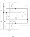
- Fig. 1 is an electrical schematic diagram of the relaxation oscillator. It can be seen from Fig. 1 that the relaxation oscillating circuit of the relaxation oscillator comprises a threshold voltage generation circuit 1, a capacitance charging and discharging circuit 2 and a comparator circuit 3; the threshold voltage generation circuit 1 outputs a threshold voltage signal to a reverse-phase input end of the comparator circuit 3; the capacitance charging and discharging circuit 2 outputs a capacitance voltage signal to an in-phase input end of the comparator circuit 3.
- the threshold voltage generation circuit 1 comprises a first current source I1, a second current source I2 and a threshold resistor R1; the first current source I1 applies current to the threshold resistor R1 through a first reverse-phase switch element SW1 (that is, the current flows to the threshold resistor R1 from the first current source I1 via the first reverse-phase switch element SW1); the second current source I2 extracts current from the threshold resistor R1 through a first in-phase switch element SW2 (that is, the current flows to the second current source I2 from the threshold resistor R1 via the first in-phase switch element SW2).
- the capacitance charging and discharging circuit 2 comprises a third current source I3, a fourth current source I4 and a capacitor C1; the third current source I3 applies current to the capacitor C1 through a second reverse-phase switch element SW3 (that is, the current flows to the capacitor C1 from the third current source I3 via the second reverse-phase switch element SW3); the fourth current source I4 extracts current from the capacitor C1 through a second in-phase switch element SW4 (that is, the current flows to the fourth current source I4 from the capacitor C1 via the second in-phase switch element SW4); wherein the first current source I1 and the third current source I3 are electrically connected with a power cord VDD respectively; the second current source I2 and the fourth current source I4 are electrically connected with a ground wire GND respectively; and the first reverse-phase switch element SW1, the first in-phase switch element SW2, the second reverse-phase switch element SW3 and the second in-phase switch element SW4 are electrically connected with an output end of the comparator circuit 3 respectively and receive an output end
- the threshold voltage generation circuit 1 is provided with the first current source I1, the second current source I2, the threshold resistor R1, as well as the first reverse-phase switch element SW1 and the first in-phase switch element SW2 which are opposite in enabled levels.
- the first current source I1 can establish I1 ⁇ R1 differential pressure with the threshold resistor R1; contrarily, the second current source I2 can establish I2 ⁇ R1 differential pressure with the threshold resistor R1.
- the capacitance charging and discharging circuit 2 is provided with the third current source I3, the fourth current source I4, the capacitor C1, as well as the second reverse-phase switch element SW3 and the second in-phase switch element SW4 which are opposite in enabled levels.
- the second reverse-phase switch element SW3 is switched on, the second in-phase switch element SW4 is cut off, and the third current source I3 can charge the capacitor C1; and contrarily, the fourth current source I4 can discharge the capacitor C1.
- Threshold voltage VR1 generated on the threshold resistor R1 by the comparator circuit 3 is compared with voltage VC1 of a charging and discharging node of the capacitor C1, control voltage Vout1 of power cord VDD end voltage or ground wire GND end voltage is output according to a comparative result, and the control voltage Vout1 is used to control voltage of a reference end of the threshold resistor R1 and voltage of a reference end of the capacitor C1 and to control conducting states of switches.
- the working principle of the relaxation oscillating circuit is as follows: It is contemplated that the capacitor C1 is not charged initially, and Vout1 is the ground wire GND voltage VGND. Firstly, the first reverse-phase switch element SW1 and the second reverse-phase switch element SW3 are switched on, the threshold voltage VR1 is established by the first current source I1, the capacitor C1 is charged by the third current source I3, and capacitor voltage VC1 rises.
- the control voltage Vout1 When the capacitor voltage VC1 exceeds the threshold voltage VR1, the control voltage Vout1 is turned into supply voltage VDD, the voltage of the reference ends of the resistor R1 and the capacitor C1 is turned into the supply voltage VDD to achieve bootstrap, by this time, the control voltage Vout1 is in a high level state, the first reverse-phase switch element SW1 and the second reverse-phase switch element SW3 are cut off when the control voltage Vout1 is at a high level, and the first in-phase switch element SW2, and the second in-phase switch element SW4 are switched on when the control voltage Vout1 is at the high level,
- the threshold voltage VR1 is established by the second current source I2
- the capacitor voltage VC1 is bootstrapped, then turned into VR1 plus VDD, discharging is carried out by the fourth current source I4, and the capacitor voltage VC1 falls
- the control voltage Vout1 output by a comparator When the capacitor voltage Vout1 is lower than the threshold voltage VR1, the control voltage Vout1 output by a comparator
- the threshold voltage VR1 is established by the first current source 11, and the capacitor voltage VC1 is bootstrapped and then turned into VR1 minus VDD, and rises after being charged by the third current source I3.
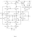
- Fig. 2 is an electrical schematic diagram of another Embodiment of the relaxation oscillator.
- the relaxation oscillating circuit comprises a biasing circuit; the biasing circuit comprises a reference current source IR, a fifth NMOS transistor MN5, a sixth NMOS transistor MN6 and a fifth PMOS transistor MP5, wherein the reference current source IR is electrically connected with the power cord VDD; the reference current source IR is electrically connected with a drain electrode and a gate electrode of the fifth NMOS transistor MN5; the gate electrode of the fifth NMOS transistor MN5 is electrically connected with a gate electrode of the sixth NMOS transistor MN6; a drain electrode and a gate electrode of the fifth PMOS transistor MP5 are electrically connected with a drain electrode of the sixth NMOS transistor MN6.
- the biasing circuit forms a mirror current source through the reference current source IR, the fifth NMOS transistor MN5, the sixth NMOS transistor MN6 and the fifth PMOS transistor MP5
- the gate electrode of the fifth PMOS transistor MP5 is electrically connected with a gate electrode of a first PMOS transistor MP1 and a gate electrode of a second PMOS transistor MP2 respectively, and a source electrode of the first PMOS transistor MP1 and a source electrode of the second PMOS transistor MP2 are electrically connected with the power cord VDD respectively, so that the biasing circuit and the first PMOS transistor MP1 form a current source for providing current for a resistor R2 in a charging process, and the biasing circuit and the second PMOS transistor MP2 form a current source for providing current for a capacitor C2 in the charging process.
- the gate electrode of the fifth NMOS transistor MN5 is electrically connected with a gate electrode of a first NMOS transistor MN1 and a gate electrode of a second NMOS transistor MN2 respectively.
- a source electrode of the first NMOS transistor MN1 is electrically connected with the ground wire GND, so that the biasing circuit and the first NMOS transistor MN1 form a current source for providing current for the resistor R2 in a discharging process; and a source electrode of the second NMOS transistor MN2 is electrically connected with the ground wire GND, so that the biasing circuit and the second NMOS transistor MN2 form a current source for providing current for the capacitor C2 in the discharging process.
- the comparator circuit of the oscillating circuit comprises a current mode comparator circuit and a phase inverter circuit; the current mode comparator circuit transmits a voltage signal to the phase inverter circuit; wherein the current mode comparator circuit comprises a first current mode comparison circuit and a second current mode comparison circuit.
- the first current mode comparison circuit and the second current mode comparison circuit are electrically connected with a first input end and a second input end of the comparator circuit; in this Embodiment, the first input end of the comparator circuit inputs voltage VR2 to a reference end of the resistor R2; the second input end inputs voltage VC2 to a reference end of the capacitor C2; the first current mode comparison circuit is used for comparing voltage VR2 of the reference end of the resistor R2 and voltage VC2 of the reference end of the capacitor C2 in the charging process. and the second current mode comparison circuit is used for comparing voltage VR2 of the reference end of the resistor R2 and voltage VC2 of the reference end of the capacitor C2 in the discharging process.
- the first current mode comparison circuit comprises a current mode comparator consisting of a third NMOS transistor MN3 and a fourth NMOS transistor MN4; a gate electrode and a drain electrode of the third NMOS transistor MN3 are electrically connected with a gate electrode of the fourth NMOS transistor MN4; the drain electrode of the third NMOS transistor MN3 is electrically connected with a drain electrode of the first PMOS transistor MP1; a drain electrode of the fourth NMOS transistor MN4 is electrically connected with a drain electrode of the second PMOS transistor NW2; a source electrode of the third NMOS transistor MN3 is electrically connected with the resistor R2 through a switch element SW5; and a source electrode of the fourth NMOS transistor MN4 is electrically connected with the capacitor C2 through a switch element SW7.
- a current mode comparator consisting of a third NMOS transistor MN3 and a fourth NMOS transistor MN4; a gate electrode and a drain electrode of the third NMOS transistor M
- the second current mode comparison circuit comprises a current mode comparator consisting of a third PMOS transistor MP3 and a fourth PMOS transistor MP4; a gate electrode and a drain electrode of the third PMOS transistor MP3 are electrically connected with a gate electrode of the fourth PMOS transistor MP4; the drain electrode of the third PMOS transistor MP3 is electrically connected with a drain electrode of the first NMOS transistor MN1; a drain electrode of the fourth PMOS transistor NW4 is electrically connected with a drain electrode of the second NMOS transistor MN2; a source electrode of the third PMOS transistor MP3 is electrically connected with the resistor R2 through a switch element SW6; and a source electrode of the fourth PMOS transistor NW4 is electrically connected with the capacitor C2 through a switch element SW8.
- the phase inverter circuit comprises a phase inverter Inv1 and a phase inverter Inv2; the phase inverter Inv1 is connected with the phase inverter Inv2 in series; an input end of the phase inverter Inv1 is electrically connected with the drain electrode of the fourth NMOS transistor MN4 through a switch element SW9; the input end of the phase inverter Inv1 is electrically connected with the drain electrode of the fourth PMOS transistor NW4 through a switch element SW10; after the voltage VR2 of the resistor R2 and the voltage VC2 of the capacitor C2 are compared by the first current mode comparison circuit or the second current mode comparison circuit, voltage VP is obtained; and the voltage VP is input to the phase inverter Inv1, quantized by the phase inverter Inv1, and then subjected to wave shaping by the phase inverter Inv2 to be obtain voltage Vout2.
- phase inverter circuit is used in the comparator circuit because after the bootstrap technique is adopted, even if the phase inverters has unstable turn threshold voltage, only a duty ratio is affected, while the influence on the oscillating cycle is little, so that a situation that a comparator relatively high in power dissipation is used to eliminate offset voltage is avoided.
- phase inverters are used to achieve generation of comparator and digital control logic, both the design complexity and the power dissipation are lowered, and at the same time, the comparator realized by the phase inverters automatically eliminate influence on the threshold voltage of the comparator by the offset voltage and temperature change in a working process and thus lowers the limitation to the frequency stability.
- switch element SW5, the switch element SW6, the switch element SW7, the switch element SW8, the switch element SW9 and the switch element SW10 are respectively fed with control signals by the output end of the phase inverter Inv2, and can control switch-on states of the switches according to the voltage Vout2 of the output end of the phase inverter Inv2.
- the switch element SW5, the switch element SW7 and the switch element SW9 are reverse-phase switch elements, and are cut off when the voltage Vout2 is at a high level and switched on when the voltage Vout2 is at a low level;
- the switch element SW6, the switch element SW8 and the switch element SW10 are in-phase switch elements, and are switched on when the voltage Vout2 is at the high level and cut off when the voltage Vout2 is at the low level.
- a branch circuit between the resistor R2 and the capacitor C2 is electrically connected with the voltage Vout2 of the output end of the phase inverter Inv2, and the output voltage Vout2 is fed back to the branch circuit between the threshold resistor and the capacitor, so that the current utilization rate is increased.
- a voltage wave diagram of voltage VC2 of the reference end of the capacitor C2 is shown. It is contemplated that all current provided by the current sources is equal to I.
- the voltage of the reference end of the resistor R2 is VR2 which is equal to I ⁇ R2
- the voltage of the reference end of capacitor C2 immediately lifts VDD due to the function of bootstrap, so VC2 is equal to VDD+I ⁇ R2, and subsequently the capacitor C2 is discharged
- the voltage of the reference end of the resistor R2 is VR2 which is equal to VDD-I ⁇ R2
- after VC2 is equal to VDD-I ⁇ R2 as a result of discharging the capacitor C2
- the voltage of the reference end of capacitor C2 immediately lowers VDD due to the function of bootstrap, so VC2 is equal to -I ⁇ R2,
- VC2 has a variation of 2 ⁇ I ⁇ R2 during charging the capacitor C2
- VC2 also has a variation of 2 ⁇ I ⁇ R2 during discharging
- the sum of the variations of VC2 is ⁇ V which is equal to 4 ⁇ I ⁇ R2.
- this computing method is certainly applicable to Embodiment 1.
- the relaxation oscillator is simple in structure, few in module, low in power dissipation, and high in current utilization rate, so that the effects of shortening a development cycle, reducing a layout area of a circuit board and achieving super-low power dissipation are realized.
- the first comparison circuit of the comparator circuit consists of in common-gate connection MOS transistors, so a voltage magnification effect is played; and the output voltage Vout2 is fed back to the branch circuit between the threshold resistor R2 and the capacitor C2, so that the current utilization rate is increased.
- Fig. 4 is an electrical schematic diagram of Embodiment 3 of the relaxation oscillator.
- the relaxation oscillating circuit comprises a biasing circuit; the biasing circuit comprises a reference current source IR1, an NMOS transistor MN51, an NMOS transistor MN61 and a PMOS transistor MP51, wherein the reference current source IR1 is electrically connected with the power cord VDD; the reference current source IR1 is electrically connected with a drain electrode and a gate electrode of the NMOS transistor MN51; the gate electrode of the NMOS transistor MN51 is electrically connected with a gate electrode of the NMOS transistor MN61; a drain electrode and a gate electrode of the PMOS transistor MP51 are electrically connected with a drain electrode of the NMOS transistor MN61.
- the biasing circuit forms a mirror current source through the reference current source IR1, the NMOS transistor MN51, the NMOS transistor MN61 and the PMOS transistor MP51, and provides bias current for an oscillating circuit.
- the gate electrode of the PMOS transistor MP51 are electrically connected with a gate electrode of a PMOS transistor MP11 and a gate electrode of a PMOS transistor MP21 respectively, and a source electrode of the PMOS transistor MP11 and a source electrode of the PMOS transistor MP21 are electrically connected with the power cord VDD respectively, so that the biasing circuit and the PMOS transistor MP11 form a current source for providing current for a resistor R3 in a charging process, and the biasing circuit and the PMOS transistor MP21 form a current source for providing current for a capacitor C3 in the charging process.
- the gate electrode of the NMOS transistor MN51 is electrically connected with a gate electrode of an NMOS transistor MN11 and a gate electrode of an NMOS transistor MN21 respectively; a source electrode of the NMOS transistor MN11 is electrically connected with the ground wire GND, so that the biasing circuit and the NMOS transistor MN11 form a current source for providing current for the resistor R3 in a discharging process; and a source electrode of the NMOS transistor MN21 is electrically connected with the ground wire GND, so that the biasing circuit and the NMOS transistor MN21 form a current source for providing current for the capacitor C3 in the discharging process.
- the comparator circuit of the oscillating circuit comprises a current mode comparator circuit and a voltage comparison circuit; wherein the current mode comparator circuit comprises a first current mode comparison circuit and a second current mode comparison circuit.
- the first current mode comparison circuit is used for comparing voltage VR3 of a reference end of the resistor R3 and voltage VC3 of a reference end of the capacitor C3 in a charging process; and the second current mode comparison circuit is used for comparing voltage VR3 of the reference end of the resistor R3 and voltage VC3 of the reference end of the capacitor C3 in a discharging process.
- the first current mode comparison circuit comprises a current mode comparator consisting of an NMOS transistor MN31 and an NMOS transistor MN41; a gate electrode and a drain electrode of the NMOS transistor MN31 are electrically connected with a gate electrode of the NMOS transistor MN41; the drain electrode of the NMOS transistor MN31 is electrically connected with a drain electrode of the PMOS transistor MP11; a drain electrode of the NMOS transistor MN41 is electrically connected with a drain electrode of the PMOS transistor MP21; a source electrode of the NMOS transistor MN31 is electrically connected with the resistor R3 through a switch element SW13; and a source electrode of the NMOS transistor MN41 is electrically connected with the capacitor C3 through a switch element SW15.
- the second current mode comparison circuit comprises a current mode comparator consisting of a PMOS transistor MP31 and a PMOS transistor MP41; a gate electrode and a drain electrode of the PMOS transistor NW31 are electrically connected with a gate electrode of the PMOS transistor MP41; the drain electrode of the PMOS transistor NW31 is electrically connected with a drain electrode of the NMOS transistor MN11; a drain electrode of the PMOS transistor MP41 is electrically connected with a drain electrode of the NMOS transistor MN21; a source electrode of the PMOS transistor NW31 is electrically connected with the resistor R3 through a switch element SW14; and a source electrode of the PMOS transistor NW41 is electrically connected with the capacitor C3 through a switch element SW16.
- a reverse-phase input end of the voltage comparison circuit U2 is electrically connected with the drain electrode of the NMOS transistor MN31 through a switch element SW11; the reverse-phase input end of the voltage comparison circuit U2 is electrically connected with the drain electrode of the PMOS transistor NW31 through a switch element SW12.
- An in-phase input end of the voltage comparison circuit U2 is electrically connected with the drain electrode of the NMOS transistor MN41 through a switch element SW17; the in-phase input end of the voltage comparison circuit U2 is electrically connected with the drain electrode of the PMOS transistor MP41 through a switch element SW18.
- an output end of the voltage comparison circuit U2 provides control signals for the switch element SW11, the switch element SW12, the switch element SW13, the switch element SW14, the switch element SW15, the switch element SW16, the switch element SW17 and the switch element SW18 respectively, wherein the switch element SW11, the switch element SW13, the switch element SW15 and the switch element SW17 are reverse-phase switch elements, and the switch element SW12, the switch element SW14, the switch element SW16 and the switch element SW18 are in-phase switch element.
- the first current mode comparison circuit or the second current mode comparison circuit outputs a first voltage signal to the reverse-phase input end of the voltage comparison circuit U2, and the first current mode comparison circuit or the second current mode comparison circuit outputs a second voltage signal to the in-phase input end of the voltage comparison circuit U2.
- voltage VN is output at the drain electrode of the NMOS transistor MN31 or the drain electrode of the PMOS transistor MP31
- voltage VP1 is output at the drain electrode of the NMOS transistor MN41 or the drain electrode of the PMOS transistor MP41.
- the voltage VN is input to the reverse-phase input end of the voltage comparison circuit U2, the voltage VP1 is input to the in-phase input end of the voltage comparison circuit U2, and output voltage Vout3 is obtained at the output end of the voltage comparison circuit U2.
- the switch element SW17, the switch element SW18, switch element SW11 and the switch element SW12 can control switch-on states of the switches according the output voltage Vout3 of the output end of the voltage comparison circuit U2.
- switch element SW17 and the switch element SW11 are cut off when the voltage Vout3 is at a high level and switched on when the voltage Vout2 is at a low level; and the switch element SW18 and the switch element SW12 are cut off when the voltage Vout3 is at the low level and switched on when the voltage Vout3 is at the high level.
- the relaxation oscillator can provide a clock signal at stable frequency for a clock using circuit in the monolithic integrated chip, wherein the clock using circuit is a circuit necessarily initiated by the clock signal, such as a digital circuit under sequential control.
- this oscillator is simple in structure, few in module, low in power dissipation and high in current utilization rate, resulting in that the monolithic integrated chip can realize high frequency stability and low power dissipation.
- the invention is defined by claim 1.
- the comparator of the invention takes the MOS transistors which are in common-gate connection as the current mode comparison circuits, so that the voltage amplification effect is proved without consuming extra power dissipation, and the circuit performance is improved.
- the comparator of the invention uses the simplest digital logic phase inverters to achieve comparator and generation of digital control logic, so that the design complexity and the power dissipation are lowered simultaneously.
- the comparator can automatically eliminate influence from offset voltage and temperature change in a working process.
- the relaxation oscillator of the invention feeds back output voltage of the comparator to the branch circuit between the threshold resistor and the capacitor, leading to that the voltage ranges of capacitor charging and discharging are extended; and after being charged, the capacitor discharges with existing charges, thereby increasing the current utilization rate.
Landscapes
- Physics & Mathematics (AREA)
- Nonlinear Science (AREA)
- Manipulation Of Pulses (AREA)
Claims (3)
- Oscillateur à relaxation comprenant un comparateur, le comparateur comprenant un circuit comparateur (3), dans lequel le circuit comparateur (3) comprend un circuit comparateur de mode de courant, dans lequel le circuit comparateur de mode de courant comprend un premier circuit de comparaison de mode de courant et un deuxième circuit de comparaison de mode de courant, et à la fois le premier circuit de comparaison de mode de courant et le deuxième circuit de comparaison de mode de courant sont électriquement connectés à une première extrémité d'entrée et à une deuxième extrémité d'entrée du circuit comparateur (3) ; etle premier circuit de comparaison de mode de courant comprend deux transistors MOS de type N (MN3, MN4, MN31, MN41), les électrodes de grille des deux transistors MOS de type N (MN3, MN4, MN31, MN41) sont électriquement connectées les unes aux autres, le deuxième circuit de comparaison de mode de courant comprend deux transistors MOS de type P (MP3, MP4, MP31, MP41), et les électrodes de grille des deux transistors MOS de type P (MP3, MP4, MP31, MP41) sont électriquement connectées les unes aux autres ;dans lequel le circuit comparateur (3) comprend en outre un circuit inverseur de phase, et le circuit comparateur de mode de courant transmet des signaux de tension au circuit inverseur de phase ;le circuit inverseur de phase comprend un premier inverseur de phase (Inv1) et un deuxième inverseur de phase (Inv2), et le premier inverseur de phase (Inv1) est connecté au deuxième inverseur de phase (Inv2) en série ; etune extrémité de sortie du premier circuit de comparaison de mode de courant et une extrémité de sortie du deuxième circuit de comparaison de mode de courant sont électriquement connectées à une extrémité d'entrée du premier inverseur de phase (Inv1), respectivement;l'oscillateur à relaxation comprend en outre un circuit d'oscillation de relaxation, dans lequel le circuit d'oscillation de relaxation comprend en outre un circuit de génération de tension de seuil (1) et un circuit de charge et de décharge de capacité (2), le circuit de génération de tension de seuil (1) entre un signal de tension de seuil dans la première extrémité d'entrée du circuit comparateur (3), et le circuit de charge et de décharge de capacité (2) entre un signal de tension de capacité dans la deuxième extrémité d'entrée du circuit comparateur (3) ;dans lequel le circuit de génération de tension de seuil (1) comprend une première source de courant (I1), une deuxième source de courant (I2) et une résistance de seuil (R1), dans lequel la première source de courant (I1) est connectée électriquement à la résistance de seuil (R1) par l'intermédiaire d'un premier élément de commutation (SW1), et la deuxième source de courant (I2) est connectée électriquement à la résistance de seuil (R1) par l'intermédiaire d'un deuxième élément de commutation (SW2) ; etle circuit de charge et de décharge de capacité (2) comprend une troisième source de courant (I3), une quatrième source de courant (I4) et un condensateur (C1), dans lequel la troisième source de courant (I3) est connectée électriquement au condensateur (C1) par l'intermédiaire d'un troisième élément de commutation (SW3), et la quatrième source de courant (I4) est connectée électriquement au condensateur (C1) par l'intermédiaire d'un quatrième élément de commutation (SW4) ;caractérisé en ce quele premier élément de commutation (SW1), le deuxième élément de commutation (SW2), le troisième élément de commutation (SW3) et le quatrième élément de commutation (SW4) sont connectés électriquement à une extrémité de sortie du circuit comparateur (3), respectivement ;l'extrémité de sortie du circuit comparateur (3) est connectée électriquement à un circuit de dérivation entre la résistance de seuil (R1) et le condensateur (C1) ; etla première source de courant (I1) et la troisième source de courant (I3) sont connectées électriquement à un cordon d'alimentation (VDD), respectivement, et la deuxième source de courant (I2) et la quatrième source de courant (I4) sont connectées électriquement à un fil de masse (GND), respectivement.
- Oscillateur à relaxation selon la revendication 1, dans lequel le circuit comparateur (3) comprend en outre un circuit de comparaison de tension (U2), le premier circuit de comparaison de mode de courant ou le deuxième circuit de comparaison de mode de courant émet un premier signal de tension vers une extrémité d'entrée en phase inverse du circuit de comparaison de tension (U2), et le premier circuit de comparaison de mode de courant ou le deuxième circuit de comparaison de mode de courant émet un deuxième signal de tension vers une extrémité d'entrée en phase du circuit de comparaison de tension (U2).
- Oscillateur à relaxation selon la revendication 1, dans lequel la première source de courant, la deuxième source de courant, la troisième source de courant et la quatrième source de courant sont chacune munie d'un transistor MOS (MP11, MN11, MP21, MN21), le transistor MOS (MP11) de la première source de courant est en connexion de grille commune avec le transistor MOS (MP21) de la troisième source de courant, et le transistor MOS (MN11) de la deuxième source de courant est en connexion de grille commune avec le transistor MOS (MN21) de la quatrième source de courant.
Applications Claiming Priority (2)
| Application Number | Priority Date | Filing Date | Title |
|---|---|---|---|
| CN201610575662.0A CN106160703B (zh) | 2016-07-20 | 2016-07-20 | 比较器及张弛振荡器 |
| PCT/CN2016/109573 WO2018014493A1 (fr) | 2016-07-20 | 2016-12-13 | Comparateur et oscillateur à relaxation |
Publications (3)
| Publication Number | Publication Date |
|---|---|
| EP3477860A1 EP3477860A1 (fr) | 2019-05-01 |
| EP3477860A4 EP3477860A4 (fr) | 2020-03-04 |
| EP3477860B1 true EP3477860B1 (fr) | 2023-05-10 |
Family
ID=58060181
Family Applications (1)
| Application Number | Title | Priority Date | Filing Date |
|---|---|---|---|
| EP16909420.8A Active EP3477860B1 (fr) | 2016-07-20 | 2016-12-13 | Comparateur et oscillateur à relaxation |
Country Status (4)
| Country | Link |
|---|---|
| US (1) | US10727822B2 (fr) |
| EP (1) | EP3477860B1 (fr) |
| CN (1) | CN106160703B (fr) |
| WO (1) | WO2018014493A1 (fr) |
Families Citing this family (8)
| Publication number | Priority date | Publication date | Assignee | Title |
|---|---|---|---|---|
| CN106209027B (zh) * | 2016-07-20 | 2019-04-09 | 珠海全志科技股份有限公司 | 张弛振荡器及单片集成芯片 |
| CN106160703B (zh) * | 2016-07-20 | 2019-05-24 | 珠海全志科技股份有限公司 | 比较器及张弛振荡器 |
| CN107222186B (zh) * | 2017-05-05 | 2019-09-24 | 西北工业大学 | 无比较器的rc张弛振荡器 |
| CN107332541B (zh) * | 2017-06-20 | 2019-09-24 | 西北工业大学 | 比较器失调抵消的rc张弛振荡器 |
| CN107508579B (zh) * | 2017-08-23 | 2019-10-22 | 西北工业大学 | 一种电荷转移rc张弛振荡器 |
| CN109039304B (zh) * | 2018-06-29 | 2022-02-22 | 南京中感微电子有限公司 | 时钟电路 |
| CN109672408B (zh) * | 2018-11-22 | 2023-02-03 | 合肥市芯海电子科技有限公司 | 一种低功耗快速起振可编程的晶体振荡器电路 |
| CN114244320B (zh) * | 2022-02-25 | 2022-05-24 | 杭州万高科技股份有限公司 | 张驰振荡电路 |
Family Cites Families (19)
| Publication number | Priority date | Publication date | Assignee | Title |
|---|---|---|---|---|
| JPS61105111A (ja) * | 1984-10-27 | 1986-05-23 | Toshiba Corp | 電圧制御発振回路 |
| US5434545A (en) * | 1994-10-21 | 1995-07-18 | Cyrix Corporation | Fully differential voltage controlled oscillator |
| US6307415B1 (en) * | 1996-09-20 | 2001-10-23 | Stmicroelectronics, Inc. | Hysteresis circuit |
| CN100407575C (zh) * | 2003-06-03 | 2008-07-30 | 因芬奈昂技术股份有限公司 | 带有用于改善线性和最大化频率的传播延迟补偿的张弛振荡器 |
| US7589559B2 (en) * | 2006-12-20 | 2009-09-15 | Silicon Image, Inc. | Current mode circuitry to modulate a common mode voltage |
| CN101257289B (zh) * | 2008-03-28 | 2011-04-20 | 华中科技大学 | 一种低功耗双电容驰张型cmos振荡器 |
| CN101741254B (zh) * | 2008-11-17 | 2014-02-19 | 立锜科技股份有限公司 | 驰返式电压转换器的负锁回路及控制方法 |
| CN101562442B (zh) * | 2009-03-30 | 2012-09-19 | Bcd半导体制造有限公司 | 抖频电路及低频三角波发生器 |
| WO2012029595A1 (fr) * | 2010-09-03 | 2012-03-08 | Semiconductor Energy Laboratory Co., Ltd. | Circuit d'oscillateur et élément à semi-conducteur utilisant le circuit d'oscillateur |
| US8581632B2 (en) * | 2012-02-08 | 2013-11-12 | Mediatek Inc. | Comparator with transition threshold tracking capability |
| CN103378830B (zh) | 2012-04-17 | 2016-08-24 | 国民技术股份有限公司 | 上电复位电路 |
| CN103580655B (zh) * | 2012-07-24 | 2017-05-17 | 飞思卡尔半导体公司 | 比较器和采用比较器的张弛振荡器 |
| US8803619B1 (en) * | 2013-01-30 | 2014-08-12 | Freescale Semiconductor, Inc. | Relaxation oscillator with self-biased comparator |
| CN103618525B (zh) * | 2013-12-06 | 2016-08-17 | 中国科学院上海微系统与信息技术研究所 | 一种电流模比较器 |
| CN203595959U (zh) * | 2013-12-13 | 2014-05-14 | 中国科学院上海微系统与信息技术研究所 | 一种基于电流模的总线接收器 |
| CN104124921B (zh) * | 2014-07-02 | 2017-02-15 | 浙江大学 | 基于电流模比较器的低压低功耗cmos张弛振荡器及方法 |
| CN105515550B (zh) * | 2016-01-22 | 2017-12-29 | 英麦科(厦门)微电子科技有限公司 | 一种具有高稳定度的超低功耗时钟电路 |
| CN106209027B (zh) * | 2016-07-20 | 2019-04-09 | 珠海全志科技股份有限公司 | 张弛振荡器及单片集成芯片 |
| CN106160703B (zh) * | 2016-07-20 | 2019-05-24 | 珠海全志科技股份有限公司 | 比较器及张弛振荡器 |
-
2016
- 2016-07-20 CN CN201610575662.0A patent/CN106160703B/zh active Active
- 2016-12-13 EP EP16909420.8A patent/EP3477860B1/fr active Active
- 2016-12-13 WO PCT/CN2016/109573 patent/WO2018014493A1/fr unknown
- 2016-12-13 US US16/318,888 patent/US10727822B2/en active Active
Also Published As
| Publication number | Publication date |
|---|---|
| WO2018014493A1 (fr) | 2018-01-25 |
| US20190190503A1 (en) | 2019-06-20 |
| US10727822B2 (en) | 2020-07-28 |
| CN106160703B (zh) | 2019-05-24 |
| EP3477860A1 (fr) | 2019-05-01 |
| EP3477860A4 (fr) | 2020-03-04 |
| CN106160703A (zh) | 2016-11-23 |
Similar Documents
| Publication | Publication Date | Title |
|---|---|---|
| EP3477860B1 (fr) | Comparateur et oscillateur à relaxation | |
| CN106209027B (zh) | 张弛振荡器及单片集成芯片 | |
| US8049553B2 (en) | High-voltage CMOS charge pump | |
| JP3660906B2 (ja) | 昇圧電圧の調節が可能な昇圧回路及び昇圧電圧を生成する方法並びにそれを具備する集積回路 | |
| JP2001284535A (ja) | 半導体集積回路 | |
| TWI283096B (en) | Constant current circuit and charging pump circuit of ring oscillator | |
| US8786324B1 (en) | Mixed voltage driving circuit | |
| CN210431389U (zh) | 振荡电路和集成电路 | |
| JPS62250591A (ja) | バイアス装置 | |
| CN108494385B (zh) | 低频振荡电路及偏置电压和电流产生电路 | |
| KR0167692B1 (ko) | 반도체 메모리장치의 차아지 펌프회로 | |
| JPH0159772B2 (fr) | ||
| Abaravicius et al. | High-efficiency high voltage hybrid charge pump design with an improved chip area | |
| JP2002290230A (ja) | Cmosインバータ | |
| CN110336558B (zh) | 振荡电路和集成电路 | |
| CN112953526A (zh) | 一种环形振荡电路、方法以及集成芯片 | |
| CN210490799U (zh) | 一种SoC内置振荡电路 | |
| JPH11308856A (ja) | チャージポンプ回路装置 | |
| US6249151B1 (en) | Inverter for outputting high voltage | |
| CN113839649A (zh) | 张弛振荡器、集成电路和电子设备 | |
| CN108599745B (zh) | 单电容占空比可控振荡器 | |
| JP2003283307A (ja) | Cr発振回路 | |
| TWI418137B (zh) | 電壓控制振盪器 | |
| CN107196606B (zh) | 一种振荡器 | |
| US11569738B1 (en) | Multi-stage charge pump with clock-controlled initial stage and shifted clock-controlled additional stage |
Legal Events
| Date | Code | Title | Description |
|---|---|---|---|
| STAA | Information on the status of an ep patent application or granted ep patent |
Free format text: STATUS: THE INTERNATIONAL PUBLICATION HAS BEEN MADE |
|
| PUAI | Public reference made under article 153(3) epc to a published international application that has entered the european phase |
Free format text: ORIGINAL CODE: 0009012 |
|
| STAA | Information on the status of an ep patent application or granted ep patent |
Free format text: STATUS: REQUEST FOR EXAMINATION WAS MADE |
|
| STAA | Information on the status of an ep patent application or granted ep patent |
Free format text: STATUS: REQUEST FOR EXAMINATION WAS MADE |
|
| 17P | Request for examination filed |
Effective date: 20190123 |
|
| AK | Designated contracting states |
Kind code of ref document: A1 Designated state(s): AL AT BE BG CH CY CZ DE DK EE ES FI FR GB GR HR HU IE IS IT LI LT LU LV MC MK MT NL NO PL PT RO RS SE SI SK SM TR |
|
| AX | Request for extension of the european patent |
Extension state: BA ME |
|
| DAV | Request for validation of the european patent (deleted) | ||
| DAX | Request for extension of the european patent (deleted) | ||
| REG | Reference to a national code |
Ref country code: DE Ref legal event code: R079 Ref document number: 602016079438 Country of ref document: DE Free format text: PREVIOUS MAIN CLASS: H03K0003012000 Ipc: H03K0003023100 |
|
| A4 | Supplementary search report drawn up and despatched |
Effective date: 20200205 |
|
| RIC1 | Information provided on ipc code assigned before grant |
Ipc: H03K 3/0231 20060101AFI20200130BHEP Ipc: H03K 5/24 20060101ALI20200130BHEP |
|
| STAA | Information on the status of an ep patent application or granted ep patent |
Free format text: STATUS: EXAMINATION IS IN PROGRESS |
|
| STAA | Information on the status of an ep patent application or granted ep patent |
Free format text: STATUS: EXAMINATION IS IN PROGRESS |
|
| 17Q | First examination report despatched |
Effective date: 20211126 |
|
| GRAP | Despatch of communication of intention to grant a patent |
Free format text: ORIGINAL CODE: EPIDOSNIGR1 |
|
| STAA | Information on the status of an ep patent application or granted ep patent |
Free format text: STATUS: GRANT OF PATENT IS INTENDED |
|
| INTG | Intention to grant announced |
Effective date: 20221220 |
|
| GRAS | Grant fee paid |
Free format text: ORIGINAL CODE: EPIDOSNIGR3 |
|
| GRAA | (expected) grant |
Free format text: ORIGINAL CODE: 0009210 |
|
| STAA | Information on the status of an ep patent application or granted ep patent |
Free format text: STATUS: THE PATENT HAS BEEN GRANTED |
|
| AK | Designated contracting states |
Kind code of ref document: B1 Designated state(s): AL AT BE BG CH CY CZ DE DK EE ES FI FR GB GR HR HU IE IS IT LI LT LU LV MC MK MT NL NO PL PT RO RS SE SI SK SM TR |
|
| REG | Reference to a national code |
Ref country code: GB Ref legal event code: FG4D |
|
| REG | Reference to a national code |
Ref country code: AT Ref legal event code: REF Ref document number: 1567729 Country of ref document: AT Kind code of ref document: T Effective date: 20230515 Ref country code: CH Ref legal event code: EP |
|
| REG | Reference to a national code |
Ref country code: DE Ref legal event code: R096 Ref document number: 602016079438 Country of ref document: DE |
|
| REG | Reference to a national code |
Ref country code: IE Ref legal event code: FG4D |
|
| REG | Reference to a national code |
Ref country code: DE Ref legal event code: R082 Ref document number: 602016079438 Country of ref document: DE Representative=s name: ALPSPITZ IP ALLGAYER UND PARTNER PATENTANWAELT, DE |
|
| REG | Reference to a national code |
Ref country code: LT Ref legal event code: MG9D |
|
| REG | Reference to a national code |
Ref country code: NL Ref legal event code: MP Effective date: 20230510 |
|
| REG | Reference to a national code |
Ref country code: AT Ref legal event code: MK05 Ref document number: 1567729 Country of ref document: AT Kind code of ref document: T Effective date: 20230510 |
|
| PG25 | Lapsed in a contracting state [announced via postgrant information from national office to epo] |
Ref country code: SE Free format text: LAPSE BECAUSE OF FAILURE TO SUBMIT A TRANSLATION OF THE DESCRIPTION OR TO PAY THE FEE WITHIN THE PRESCRIBED TIME-LIMIT Effective date: 20230510 Ref country code: PT Free format text: LAPSE BECAUSE OF FAILURE TO SUBMIT A TRANSLATION OF THE DESCRIPTION OR TO PAY THE FEE WITHIN THE PRESCRIBED TIME-LIMIT Effective date: 20230911 Ref country code: NO Free format text: LAPSE BECAUSE OF FAILURE TO SUBMIT A TRANSLATION OF THE DESCRIPTION OR TO PAY THE FEE WITHIN THE PRESCRIBED TIME-LIMIT Effective date: 20230810 Ref country code: NL Free format text: LAPSE BECAUSE OF FAILURE TO SUBMIT A TRANSLATION OF THE DESCRIPTION OR TO PAY THE FEE WITHIN THE PRESCRIBED TIME-LIMIT Effective date: 20230510 Ref country code: ES Free format text: LAPSE BECAUSE OF FAILURE TO SUBMIT A TRANSLATION OF THE DESCRIPTION OR TO PAY THE FEE WITHIN THE PRESCRIBED TIME-LIMIT Effective date: 20230510 Ref country code: AT Free format text: LAPSE BECAUSE OF FAILURE TO SUBMIT A TRANSLATION OF THE DESCRIPTION OR TO PAY THE FEE WITHIN THE PRESCRIBED TIME-LIMIT Effective date: 20230510 |
|
| PG25 | Lapsed in a contracting state [announced via postgrant information from national office to epo] |
Ref country code: RS Free format text: LAPSE BECAUSE OF FAILURE TO SUBMIT A TRANSLATION OF THE DESCRIPTION OR TO PAY THE FEE WITHIN THE PRESCRIBED TIME-LIMIT Effective date: 20230510 Ref country code: PL Free format text: LAPSE BECAUSE OF FAILURE TO SUBMIT A TRANSLATION OF THE DESCRIPTION OR TO PAY THE FEE WITHIN THE PRESCRIBED TIME-LIMIT Effective date: 20230510 Ref country code: LV Free format text: LAPSE BECAUSE OF FAILURE TO SUBMIT A TRANSLATION OF THE DESCRIPTION OR TO PAY THE FEE WITHIN THE PRESCRIBED TIME-LIMIT Effective date: 20230510 Ref country code: LT Free format text: LAPSE BECAUSE OF FAILURE TO SUBMIT A TRANSLATION OF THE DESCRIPTION OR TO PAY THE FEE WITHIN THE PRESCRIBED TIME-LIMIT Effective date: 20230510 Ref country code: IS Free format text: LAPSE BECAUSE OF FAILURE TO SUBMIT A TRANSLATION OF THE DESCRIPTION OR TO PAY THE FEE WITHIN THE PRESCRIBED TIME-LIMIT Effective date: 20230910 Ref country code: HR Free format text: LAPSE BECAUSE OF FAILURE TO SUBMIT A TRANSLATION OF THE DESCRIPTION OR TO PAY THE FEE WITHIN THE PRESCRIBED TIME-LIMIT Effective date: 20230510 Ref country code: GR Free format text: LAPSE BECAUSE OF FAILURE TO SUBMIT A TRANSLATION OF THE DESCRIPTION OR TO PAY THE FEE WITHIN THE PRESCRIBED TIME-LIMIT Effective date: 20230811 |
|
| PG25 | Lapsed in a contracting state [announced via postgrant information from national office to epo] |
Ref country code: FI Free format text: LAPSE BECAUSE OF FAILURE TO SUBMIT A TRANSLATION OF THE DESCRIPTION OR TO PAY THE FEE WITHIN THE PRESCRIBED TIME-LIMIT Effective date: 20230510 |
|
| PG25 | Lapsed in a contracting state [announced via postgrant information from national office to epo] |
Ref country code: SK Free format text: LAPSE BECAUSE OF FAILURE TO SUBMIT A TRANSLATION OF THE DESCRIPTION OR TO PAY THE FEE WITHIN THE PRESCRIBED TIME-LIMIT Effective date: 20230510 |
|
| PGFP | Annual fee paid to national office [announced via postgrant information from national office to epo] |
Ref country code: GB Payment date: 20231220 Year of fee payment: 8 |
|
| PG25 | Lapsed in a contracting state [announced via postgrant information from national office to epo] |
Ref country code: SM Free format text: LAPSE BECAUSE OF FAILURE TO SUBMIT A TRANSLATION OF THE DESCRIPTION OR TO PAY THE FEE WITHIN THE PRESCRIBED TIME-LIMIT Effective date: 20230510 Ref country code: SK Free format text: LAPSE BECAUSE OF FAILURE TO SUBMIT A TRANSLATION OF THE DESCRIPTION OR TO PAY THE FEE WITHIN THE PRESCRIBED TIME-LIMIT Effective date: 20230510 Ref country code: RO Free format text: LAPSE BECAUSE OF FAILURE TO SUBMIT A TRANSLATION OF THE DESCRIPTION OR TO PAY THE FEE WITHIN THE PRESCRIBED TIME-LIMIT Effective date: 20230510 Ref country code: EE Free format text: LAPSE BECAUSE OF FAILURE TO SUBMIT A TRANSLATION OF THE DESCRIPTION OR TO PAY THE FEE WITHIN THE PRESCRIBED TIME-LIMIT Effective date: 20230510 Ref country code: DK Free format text: LAPSE BECAUSE OF FAILURE TO SUBMIT A TRANSLATION OF THE DESCRIPTION OR TO PAY THE FEE WITHIN THE PRESCRIBED TIME-LIMIT Effective date: 20230510 Ref country code: CZ Free format text: LAPSE BECAUSE OF FAILURE TO SUBMIT A TRANSLATION OF THE DESCRIPTION OR TO PAY THE FEE WITHIN THE PRESCRIBED TIME-LIMIT Effective date: 20230510 |
|
| PGFP | Annual fee paid to national office [announced via postgrant information from national office to epo] |
Ref country code: FR Payment date: 20231219 Year of fee payment: 8 Ref country code: DE Payment date: 20231214 Year of fee payment: 8 |
|
| REG | Reference to a national code |
Ref country code: DE Ref legal event code: R097 Ref document number: 602016079438 Country of ref document: DE |
|
| PLBE | No opposition filed within time limit |
Free format text: ORIGINAL CODE: 0009261 |
|
| STAA | Information on the status of an ep patent application or granted ep patent |
Free format text: STATUS: NO OPPOSITION FILED WITHIN TIME LIMIT |
|
| 26N | No opposition filed |
Effective date: 20240213 |
|
| PG25 | Lapsed in a contracting state [announced via postgrant information from national office to epo] |
Ref country code: SI Free format text: LAPSE BECAUSE OF FAILURE TO SUBMIT A TRANSLATION OF THE DESCRIPTION OR TO PAY THE FEE WITHIN THE PRESCRIBED TIME-LIMIT Effective date: 20230510 |