EP3477320B1 - Apparatus for processing signals of a high-voltage loop, detector, battery device, and vehicle - Google Patents
Apparatus for processing signals of a high-voltage loop, detector, battery device, and vehicle Download PDFInfo
- Publication number
- EP3477320B1 EP3477320B1 EP18201825.9A EP18201825A EP3477320B1 EP 3477320 B1 EP3477320 B1 EP 3477320B1 EP 18201825 A EP18201825 A EP 18201825A EP 3477320 B1 EP3477320 B1 EP 3477320B1
- Authority
- EP
- European Patent Office
- Prior art keywords
- resistor
- filter
- transistor
- circuit
- connects
- Prior art date
- Legal status (The legal status is an assumption and is not a legal conclusion. Google has not performed a legal analysis and makes no representation as to the accuracy of the status listed.)
- Active
Links
Images



Classifications
-
- H—ELECTRICITY
- H03—ELECTRONIC CIRCUITRY
- H03H—IMPEDANCE NETWORKS, e.g. RESONANT CIRCUITS; RESONATORS
- H03H7/00—Multiple-port networks comprising only passive electrical elements as network components
- H03H7/01—Frequency selective two-port networks
- H03H7/06—Frequency selective two-port networks including resistors
-
- G—PHYSICS
- G01—MEASURING; TESTING
- G01R—MEASURING ELECTRIC VARIABLES; MEASURING MAGNETIC VARIABLES
- G01R31/00—Arrangements for testing electric properties; Arrangements for locating electric faults; Arrangements for electrical testing characterised by what is being tested not provided for elsewhere
- G01R31/36—Arrangements for testing, measuring or monitoring the electrical condition of accumulators or electric batteries, e.g. capacity or state of charge [SoC]
-
- G—PHYSICS
- G01—MEASURING; TESTING
- G01R—MEASURING ELECTRIC VARIABLES; MEASURING MAGNETIC VARIABLES
- G01R19/00—Arrangements for measuring currents or voltages or for indicating presence or sign thereof
- G01R19/0092—Measuring current only
-
- G—PHYSICS
- G01—MEASURING; TESTING
- G01R—MEASURING ELECTRIC VARIABLES; MEASURING MAGNETIC VARIABLES
- G01R19/00—Arrangements for measuring currents or voltages or for indicating presence or sign thereof
- G01R19/25—Arrangements for measuring currents or voltages or for indicating presence or sign thereof using digital measurement techniques
-
- G—PHYSICS
- G01—MEASURING; TESTING
- G01R—MEASURING ELECTRIC VARIABLES; MEASURING MAGNETIC VARIABLES
- G01R31/00—Arrangements for testing electric properties; Arrangements for locating electric faults; Arrangements for electrical testing characterised by what is being tested not provided for elsewhere
- G01R31/36—Arrangements for testing, measuring or monitoring the electrical condition of accumulators or electric batteries, e.g. capacity or state of charge [SoC]
- G01R31/382—Arrangements for monitoring battery or accumulator variables, e.g. SoC
-
- G—PHYSICS
- G01—MEASURING; TESTING
- G01R—MEASURING ELECTRIC VARIABLES; MEASURING MAGNETIC VARIABLES
- G01R31/00—Arrangements for testing electric properties; Arrangements for locating electric faults; Arrangements for electrical testing characterised by what is being tested not provided for elsewhere
- G01R31/36—Arrangements for testing, measuring or monitoring the electrical condition of accumulators or electric batteries, e.g. capacity or state of charge [SoC]
- G01R31/382—Arrangements for monitoring battery or accumulator variables, e.g. SoC
- G01R31/3835—Arrangements for monitoring battery or accumulator variables, e.g. SoC involving only voltage measurements
-
- H—ELECTRICITY
- H03—ELECTRONIC CIRCUITRY
- H03F—AMPLIFIERS
- H03F3/00—Amplifiers with only discharge tubes or only semiconductor devices as amplifying elements
- H03F3/45—Differential amplifiers
- H03F3/45071—Differential amplifiers with semiconductor devices only
- H03F3/45076—Differential amplifiers with semiconductor devices only characterised by the way of implementation of the active amplifying circuit in the differential amplifier
- H03F3/45475—Differential amplifiers with semiconductor devices only characterised by the way of implementation of the active amplifying circuit in the differential amplifier using IC blocks as the active amplifying circuit
-
- H—ELECTRICITY
- H03—ELECTRONIC CIRCUITRY
- H03F—AMPLIFIERS
- H03F2200/00—Indexing scheme relating to amplifiers
- H03F2200/165—A filter circuit coupled to the input of an amplifier
-
- H—ELECTRICITY
- H03—ELECTRONIC CIRCUITRY
- H03F—AMPLIFIERS
- H03F2203/00—Indexing scheme relating to amplifiers with only discharge tubes or only semiconductor devices as amplifying elements covered by H03F3/00
- H03F2203/45—Indexing scheme relating to differential amplifiers
- H03F2203/45022—One or more added resistors to the amplifying transistors in the differential amplifier
-
- H—ELECTRICITY
- H03—ELECTRONIC CIRCUITRY
- H03F—AMPLIFIERS
- H03F2203/00—Indexing scheme relating to amplifiers with only discharge tubes or only semiconductor devices as amplifying elements covered by H03F3/00
- H03F2203/45—Indexing scheme relating to differential amplifiers
- H03F2203/45151—At least one resistor being added at the input of a dif amp
Definitions
- the present application relates to the battery fields and, more particularly to an apparatus for processing signals of a high-voltage loop.
- the present application further relates to a detector, a battery device, and a vehicle including an apparatus for processing signals of a high-voltage loop.
- the environment for a high-voltage loop of a power battery of the vehicle can be complicated and variable.
- devices such as cellphone and internal electric motor in the vehicle can result an environment where electromagnetic interference is in a range of a low frequency to an ultrahigh frequency.
- This can cause electromagnetic interference to the high-voltage loop of the power battery.
- a current of the high-voltage loop of the battery is detected based on a change of a magnetic field due to a change of the current.
- flux-gate current detection devices and magnetic-resistant current detection devices measure a current according to a mutual conversion relation of the current and the magnetic field. Consequently, the electromagnetic interference can affect detection accuracy of the high-voltage loop, and the real current value may not be accurately detected.
- Prior art document US 2014/0176149 A1 discloses a battery monitoring apparatus, including a plurality of connection lines, a monitoring circuit, a first filter circuit, and a second filter circuit.
- the monitoring circuit is provided with a pair of sensing terminals for each pair of positive and negative electrode terminals of each of a plurality of battery cells of a battery pack.
- the plurality of connection lines includes a plurality of common line and first and second branch lines.
- the first filter circuit includes first resistors located on the first and second branch lines connected to the pair of sensing terminals, and a first capacitor located between the first and second branch lines connected to the pair of sensing terminals.
- the second filter circuit includes a second resistor located on the plurality of connection lines, and a second capacitor connected in series between the plurality of connection lines without passing through the first resistors and the second resistor.
- Prior art document WO 2013/161870 A1 discloses an insulation abnormality detection device.
- the negative pole of a battery on a high voltage side is connected to serially connected circuits for a coupling capacitor (101), a detection resistor (102) and an oscillator (103).
- An observation signal (V2) output from the connected portion of the coupling capacitor (101) and the detection resistor (102) is input to a notch filter (104) and a subtraction circuit (105).
- the notch filter (104) receives the input of the observation signal (V2) and cuts only the component near the frequency of an oscillation signal (V1) generated by the oscillator (103).
- An output signal (Vm) of the notch filter (104) is input to the subtraction circuit (105).
- the subtraction circuit (105) executes subtraction processing between the observation signal (V2) and the output signal (Vm) of the notch filter (104).
- a determination circuit (106) compares the waveform of an output signal (Ve) of the subtraction circuit (105) to the waveform of the oscillation signal (V1) of the oscillator (103) and determines if there is an insulation abnormality.
- Prior art document EP 3 214 452 A1 discloses an abnormality detection device, including: a coupling-capacitor having a first-end and a second-end coupled with a high-voltage circuit; a signal output unit; a signal extraction unit; and a signal input unit.
- the signal output unit is coupled with the first-end of the coupling-capacitor via a detection-resistor, and outputs an alternating-current inspection-signal.
- the signal extraction unit extracts the inspection-signal, as an extraction-signal, output between the detection-resistor and the coupling-capacitor.
- the signal input unit detects abnormality of insulation resistance of the high-voltage circuit based on a level of the inputted extraction-signal.
- the signal extraction unit includes a signal removing filter and a subtraction circuit.
- the filter removes a signal equal in frequency to the inspection-signal and passes low-frequency noises lower in frequency than the inspection-signal.
- the subtraction circuit outputs a differential signal, as the extraction-signal, between a signal having passed through the filter and a signal not having passed through the filter.
- Prior art document EP 2 966 460 A1 discloses a current sampling circuit including a proportional current output circuit and a full differential common mode negative feedback circuit, specifically the proportional current output circuit is configured to calculate a current output from a power device according to a preset proportion to obtain a first proportional current and a second proportional current, and to output the first proportional current and the second proportional current to the full differential common mode negative feedback circuit; and the full differential common mode negative feedback circuit is configured to shunt respectively the first proportional current and the second proportional current using a full differential common mode negative feedback network with a bias current in microamps to obtain a first sampling current and a second sampling current, and to output constantly the first sampling current and the second sampling current. Further disclosed is a current sampling method.
- Prior art document US 2013/271216 A1 discloses a single stage current sense amplifier, which generates a differential output that is proportional to a current through a sense resistor.
- the voltage across the sense resistor is V sense.
- the current sense amplifier includes a differential transconductance amplifier having high impedance input terminals.
- An on-chip RC filter filters transients in the V sense signal.
- a feedback circuit for each leg of the amplifier causes a pair of input transistors to conduct a fixed constant current irrespective of V sense, which stabilizes the transconductance.
- a gain control resistor (Re) is coupled across terminals of the pair of input transistors and has V sense across it. The current through the gain control resistor is therefore Vsensex1/Re.
- a level shifting circuit coupled to each of the input transistors lowers a common mode voltage at an output of the amplifier. Chopper circuits at the input and output cancel any offset voltages.
- Prior art document US 6,215,302 B1 discloses a preamplifier for a resistive transducer, configured to generate an amplified output indicative of potential difference across the transducer (while the transducer is biased and in the presence of a magnetic field) and to generate a resistance signal indicative of the transducer's resistance, and a method for measuring the resistance of a resistive transducer during operation of the transducer in the presence of a changing magnetic field.
- the preamplifier preferably includes circuitry for generating a current signal indicative of the instantaneous current through the transducer and analog divider circuitry for generating the resistance signal from a signal indicative of the potential difference across the transducer and the current signal.
- the preamplifier can include circuitry for processing the analog resistance signal to generate a word of binary data indicative of a value proportional to the transducer resistance.
- the preamplifier can include a digital-to-analog (D-to-A) converter, and a comparator which receives an analog resistance signal and the output of the D-to-A converter.
- D-to-A digital-to-analog
- the output of the D-to-A converter is swept until the comparator is tripped, at which time the setting of the D-to-A converter is proportional to the transducer resistance.
- the present application provides an apparatus for processing signals of device, a detector, a battery device, and a vehicle, so as to solve a problem that the current detection in the high-voltage loop of the power battery in a vehicle is inaccurate.
- the accuracy of current detection is improved, which enables improved overall performance and reliability of the power battery of the vehicle.
- the present application provides an apparatus for processing signals of a high-voltage loop, including: a filter circuit configured to filter a signal from an element to be detected; a differential amplification circuit configured to amplify the filtered signal; and a processor configured to process the amplified signal.
- the filter circuit connects to the element to be detected.
- the differential amplification circuit connects to the filter circuit.
- the processor connects to the differential amplification circuit.
- the differential amplification circuit includes a first transistor, a second transistor, and a common-mode suppression element; wherein a first end of the common-mode suppression element connects to an emitter of the first transistor and an emitter of the second transistor, a second end of the common-mode suppression element connects to a low-voltage power supply.
- the common-mode suppression element is a constant-current source circuit.
- the constant-current source circuit includes a third transistor, a first resistor, a second resistor, and a third resistor, a collector of the third transistor connects to the emitter of the first transistor and the emitter of the second transistor, a base of the third transistor connects to a first end of the first resistor and a first end of the second resistor, and an emitter of the third transistor connects to a first end of the third resistor; a second end of the first resistor is grounded; a second end of the second resistor connects to the low-voltage power supply; and a second end of the third resistor connects to the low-voltage power supply.
- the common-mode suppression element is a common-mode suppression resistor.
- a resistance value of the common-mode suppression resistor is greater than 100k ⁇ .
- each of the first transistor, the second transistor, and the third transistor is a field-effect transistor and/or a triode transistor.
- the element to be detected is a current divider in the high-voltage loop, the current divider includes an internal resistor, two ends of the internal resistor connect to a first input end of the filter circuit and a second input end of the filter circuit, respectively.
- the filter circuit includes: a first electrostatic protection element, a first end of the first electrostatic protection element connects to the first input end of the filter circuit, a second end of the first electrostatic protection element is grounded; and/or a second electrostatic protection element, a first end of the second electrostatic protection element connects to the second input end of the filter circuit, a second end of the second electrostatic protection element is grounded.
- each of the first electrostatic protection element and the second electrostatic protection element includes one or more electrostatic protection capacitors.
- the filter circuit further includes a common-mode filter element, the common-mode filter element includes a fourth resistor, a first filter capacitor, a fifth resistor, and a second filter capacitor; wherein a first end of the fourth resistor connects to the first input end of the filter circuit, and a second end of the fourth resistor connects to a first end of the first filter capacitor; a second end of the first filter capacitor is grounded; a first end of the fifth resistor connects to the second input end of the filter circuit, a second end of the fifth resistor connects to a first end of the second filter capacitor; and a second end of the second filter capacitor is grounded.
- the common-mode filter element includes a fourth resistor, a first filter capacitor, a fifth resistor, and a second filter capacitor; wherein a first end of the fourth resistor connects to the first input end of the filter circuit, and a second end of the fourth resistor connects to a first end of the first filter capacitor; a second end of the first filter capacitor is grounded;
- the filter circuit further includes a differential-mode filter element, the differential-mode filter element includes the fourth resistor, the fifth resistor, and a third filter capacitor; wherein a first end of the third filter capacitor connects to a second end of the fourth resistor and a first input end of the differential amplification circuit, and a second end of the third filter capacitor connects to a second end of the fifth resistor and a second input end of the differential amplification circuit.
- the apparatus further includes: the element to be detected.
- the present application provides a detector including an apparatus for processing signals of a high-voltage loop according to any one of the above aspects.
- the present application provides a battery device including an apparatus for processing signals of a high-voltage loop according to any one of the above aspects.
- the present application provides a vehicle including an apparatus for processing signals of a high-voltage loop according to any one of the above aspects.
- the above technical solutions aim to solve a problem that the current detection in the high-voltage loop of the power battery in the vehicle is inaccurate and improve the accuracy of the current detection in the high-voltage loop.
- the element to be detected can include, but is not limited to, a current divider.
- the filter circuit can connect to two ends of the element to be detected in the high-voltage loop and the filter circuit can filter the electromagnetic interference. After the electromagnetic interference is filtered by the filter circuit, the original signals may be attenuated.
- a differential amplification circuit connects to the filter circuit and the filtered signals can be amplified by the differential amplification circuit. This can ensure that a processor accurately calculates a current value according to the signals amplified by the differential amplification circuit.
- the capability of anti-electromagnetic interference in the current detection process of the high-voltage loop of the power battery of a vehicle can be improved, which enables improved accuracy of current detection and improved overall performance and reliability of the power battery of the vehicle.
- FIG. 1A illustrates a block diagram of an apparatus for processing signals of a high-voltage loop according to an embodiment of the present application.
- an apparatus 100 for processing signals of a high-voltage loop includes a filter circuit 102, a differential amplification circuit 104, and a processor 106.
- the filter circuit 102 is configured to filter signals from an element to be detected202, and a first input end and a second input end of the filter circuit 102 are connected to two ends of the element to be detected 202, respectively.
- the differential amplification circuit 104 is configured to amplify the filtered signals, a first input end and a second input end of the differential amplification circuit 104 are connected to a first output end of the filter circuit 102 and a second output end of the filter circuit 102, respectively, and an output end of the differential amplification circuit 104 is connected to the processor 106.
- the processor 106 is configured to process the amplified signals, communicate with a peripheral system such as battery management system etc., and send a result of the current detection to the peripheral system for further processing.
- the two ends of the element to be detected 202 of the high-voltage loop can be connected to the filter circuit 102, respectively, to filter the electromagnetic interference by the filter circuit 102.
- the original signals may be weakened or attenuated.
- the differential amplification circuit 104 can be connected to the filter circuit 102 and the filtered signals can be amplified by the differential amplification circuit 104. This can make sure that the processor 106 accurately calculates a current value according to the amplified signals.
- a current detection result is not accurate, this may cause that the detected current value is lower than the real current value and a threshold for triggering a cutoff of the high-voltage loop is deemed as being not reached, which can result that when the real current value is too high and the high-voltage loop should be cut off.
- the high-voltage circuit and even the whole power battery cannot be cut off in time. Therefore, filtering the electromagnetic interference can improve the accuracy of the current detection.
- the capability of anti-electromagnetic interference during the current detection process in the high-voltage loop for the power battery of the vehicle is improved, the accuracy of the current detection is then improved, and an overall performance and reliability of the power battery and the vehicle are improved accordingly.
- FIG. IB illustrates a block diagram of an apparatus for processing signals of the high-voltage loop according to another embodiment of the present application.
- the apparatus for processing signals of a high-voltage loop can further include an element to be detected 202. Two ends of the element to be detected 202 are connected to the first input end of the filter circuit 102 and the second input end of the filter circuit 102, respectively.
- a form of the apparatus for processing signals of a high-voltage loop can be an integrated apparatus as shown in FIG. 1A , which is connected into the high-voltage loop by connection to the element to be detected 202 of the high-voltage loop.
- a form of the apparatus for processing signals of a high-voltage loop can be an integrated current detector that includes the element to be detected 202 and is directly connected to the high-voltage loop for current detection.
- the element to be detected 202 is a current divider in the high-voltage loop.
- the current divider includes an internal resistor, and two ends of the internal resistor are respectively connected to the first input end of the filter circuit 102 and the second input end of the filter circuit 102. More specifically, after a voltage signal is drawn via the two ends of the internal resistor, the voltage signal is filtered and differentially amplified to achieve the electromagnetic interference filtering and signal amplification and fidelity. Therefore, the processor 106 can obtain more accurate voltage signals. As a result, the processor 106 can calculate a voltage difference between the two ends of the internal resistor, which is then divided by a resistance value of the internal resistor so as to obtain an accurate current value.
- the apparatus 100 for processing signals of a high-voltage loop further includes an analog-to-digital (A/D) converter.
- the A/D converter can be integrated in the processor 106 as a part of the processor 106.
- the A/D converter can be an individual component placed between the differential amplification circuit 104 and the processor 106 and is configured to convert a received analog signal into a digital signal for further processing by the processor 106.
- FIG. 2 illustrates a circuit diagram of a filter circuit according to an embodiment of the present application.
- the filter circuit 102 includes a first electrostatic protection element C ES1 and/or a second electrostatic protection assembly C ES2 .
- a first end of the first electrostatic protection element C ES1 is connected to the first input end of the filter circuit 102.
- a second end of the first electrostatic protection element C ES1 is grounded.
- a first end of the second electrostatic protection element C ES2 is connected to the second input end of the filter circuit 102.
- a second end of the second electrostatic protection element C ES2 is grounded.
- the body or housing of the element to be detected 202 such as the current divider is usually made of metal, this can cause an electrostatic interference.
- a circuit branch extends from each of the two ends of the internal resistor of the current divider, it is desired to have electrostatic protection for each circuit branch where an electrostatic protection element is arranged to filter the electrostatic interference.
- the electrostatic protection element includes but is not limited to be an electrostatic protection capacitor. Though the electrostatic voltage can be high, its energy is low. Therefore, an electrostatic protection capacitor that can withstand a high voltage should be selected, instead of a capacitor with a high capacitance value. This can reduce the cost of the electrostatic protection capacitor.
- each of the first electrostatic protection element C ES1 and the second electrostatic protection element C ES2 includes one or more electrostatic protection capacitors. If more electrostatic protection capacitors are included in each of electrostatic protection elements, the filtering capability of the electrostatic interference is stronger. While fewer electrostatic protection capacitors are included in each of electrostatic protection elements, the level of signal attenuation of the signals is lower, which can facilitate signal transmission.
- the filter circuit 102 further includes a common-mode filter element.
- the common-mode filter element includes a fourth resistor R4, a first filter capacitor C1, a fifth resistor R5, and a second filter capacitor C2.
- a first end of the fourth resistor R4 is connected to the first input end of the filter circuit 102.
- a second end of the fourth resistor R4 is connected to a first end of the first filter capacitor C1.
- a second end of the first filter capacitor C1 is grounded.
- a first end of the fifth resistor R5 is connected to the second input end of the filter circuit 102, and a second end of the fifth resistor R5 is connected to a first end of the second filter capacitor C2.
- a second end of the second filter capacitor C2 is grounded.
- the above-described common-mode filter element is to mainly suppress a common-mode signal.
- the fourth resistor R4 and the fifth resistor R5 can generate magnetic fields in a same direction, which results in an increase of an inductance value of the fourth resistor R4 and the fifth resistor R5.
- an inductive reactance of the fourth resistor R4 and the fifth resistor R5 to the common-mode signal increases. Consequently, this enables the common-mode signal to be more significantly suppressed, thereby attenuating the common-mode signal and suppressing the noise of common-mode interference.
- the first filter capacitor C1 and the second filter capacitor C2 act as a function of filtering the noise of common-mode interference, which also allows the common-mode interference to be significantly suppressed.
- the filter circuit 102 optionally further includes a differential-mode filter element.
- the differential-mode filter element includes a fourth resistor R4 and a fifth resistor R5, and further includes a third filter capacitor C3.
- a first end of the third filter capacitor C3 is connected to a second end of the fourth resistor R4 and the first input end of the differential amplification circuit 104.
- a second end of the third filter capacitor C3 is connected to a second end of the fifth resistor R5 and the second input end of the differential amplification circuit 104.
- the above-described differential-mode filter element is to mainly suppress differential-mode signal.
- the fourth resistor R4 and the fifth resistor R5 are connected with the third filter capacitor C3 in series to form a loop.
- the fourth resistor R4 and the fifth resistor R5 have a high inductive reactance to the differential-mode high frequency interference, and the third filter capacitor C3 has a small capacitive reactance to the high frequency interference, this allows the differential-mode signal to be filtered to reduce the differential-mode interference noise, thereby suppressing the differential-mode interference noise.
- a resistance value of the fourth resistor R4 is same as a resistance value of the fifth resistor R5.
- a resistance value of the first filter capacitor C1 is same as a resistance value of the second filter capacitor C2.
- the differential amplification circuit 104 includes a first transistor T1, a second transistor T2, and a common-mode suppression element.
- a first end of the common-mode suppression element is connected to an emitter of the first transistor T1 and an emitter of the second transistor T2.
- a second end of the common-mode suppression element is connected to a low-voltage power supply.
- the low-voltage power supply herein can be an individual peripheral power supply or a storage battery of the vehicle.
- the signal is differentially amplified.
- the resistors in the differential amplification circuit and/or other resistors in the apparatus 100 for processing signals of the high-voltage loop can change with an increase of the temperature. For example, a resistance value of a thermistor with a negative temperature coefficient can decrease with an increase of the temperature. This can cause a poor stability of the overall circuits.
- the temperature change and the common-mode interference can cause the collector current of each transistor in the differential amplification circuit 104 to change.
- the common-mode interference is suppressed, there is a bonus effect that the temperature interference can also be suppressed.
- the collector current of each transistor in the differential amplification circuit 104 changes, a voltage drop of R e changes.
- a voltage of the load resistor changes.
- FIG. 4 shows an equivalent circuit for the differential-mode signal, where
- the common-mode suppression element includes but is not limited to the common-mode suppression resistors, and can also include other components, such as an inductor.
- the resistance value of the common-mode suppression resistor is greater than 100k ⁇ and can also be other values to meet actual requirements. When the common-mode suppression resistor is great enough, the common-mode suppression ratio K CMR is then great enough accordingly, thereby enabling the temperature interference to be suppressed.
- the common-mode suppression element is a constant-current source circuit.
- the resistance of the constant-current source circuit is almost infinite. Therefore, there is a very big common-mode suppression ratio K CMR for suppressing the temperature interference.
- the constant-current source circuit includes but is not limited to the common-mode suppression element as described in the present application, and any specific circuit to be described hereinafter, which can be any type of a circuit structure as long as it can provide a very big common-mode suppression ratio K CMR .
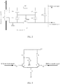
- FIG. 5 illustrates a circuit diagram of a differential amplification circuit 104 according to another embodiment of the present application.
- R e can be replaced with a third transistor T3 that is operated in a stable circuit.
- the common-mode suppression element includes the third transistor T3, a first resistor R1, a second resistor R2 and a third resistor R3.
- a collector of the third transistor T3 is connected to the emitter of the first transistor T1 and the emitter of the second transistor T2.
- a base of the third transistor T3 is connected to the first end of the first resistor R1 and the first end of the second resistor R2.
- An emitter of the third transistor T3 is connected to the first end of the third resistor R3.
- the second end of the first resistor R1 is grounded.
- the second end of the second resistor R2 is connected to the low-voltage power supply.
- the second end of the third resistor R3 is connected to the low-voltage power supply.
- the third transistor T3, the first resistor R1, the second resistor R2, and the third resistor R3 form a circuit that works at a stable point.
- the current passing through the second resistor R2 is approximately equal to the current passing through the first resistor R1.
- the voltage on the second resistor R2 is a voltage divider of the first resistor R1 and the second resistor R2. That is, the base current of the third transistor T3 is very small, and the current on the collector and the current on the emitter of the third transistor T3 are substantially the same. Therefore, the third transistor T3 can be approximately considered as a constant-current source circuit with an infinitely great internal resistance, which results that the common-mode amplification coefficient A c is 0 and thus the common-mode suppression ratio is infinitely great.
- each of the first transistor T1, the second transistor T2, and the third transistor T3 can be any one of a field-effect transistor, triode transistor, and any other type of transistors. which allows a wider range of current detection devices to be selected and decreases the production cost.
- FIG. 6 illustrates a block diagram of a detector according to an embodiment of the present application.
- a detector 600 includes an apparatus 100 for processing signals of a high-voltage loop according to any one of the embodiments as described above. Therefore, that the detector 600 has a same effect as that of the apparatus 100 for processing signals of a high-voltage loop according to any one of the embodiments as described above, which will be not repeated herein.
- the detector 600 includes but is not limited to a current detector.
- FIG. 7 illustrates a block diagram of a battery device according to an embodiment of the present application.
- a battery device 700 includes the an apparatus 100 for processing signals of a high-voltage loop according to any one of the embodiments as described above. Therefore, the battery device 700 has a same effect as that of the apparatus 100 for processing signals of a high-voltage loop according to any one of the embodiments as described above, which will be not repeated herein.
- FIG. 8 illustrates a block diagram of a vehicle according to an embodiment of the present application.
- a vehicle 800 includes the apparatus100 for processing signals of a high-voltage loop according to any one of the embodiments as described above. Therefore, the vehicle 800 has a same technical effect as that of the apparatus 100 for processing signals of a high-voltage loop according to any one of the embodiments as described above, which will be not repeated herein.
- the vehicle 800 includes but is not limited to an electric vehicle or a hybrid electric vehicle.
Landscapes
- Physics & Mathematics (AREA)
- General Physics & Mathematics (AREA)
- Engineering & Computer Science (AREA)
- Power Engineering (AREA)
- Secondary Cells (AREA)
- Measurement Of Current Or Voltage (AREA)
Priority Applications (1)
| Application Number | Priority Date | Filing Date | Title |
|---|---|---|---|
| PL18201825T PL3477320T3 (pl) | 2017-10-23 | 2018-10-22 | Urządzenie do przetwarzania sygnałów w pętli wysokiego napięcia, detektor, urządzenie akumulatorowe oraz pojazd |
Applications Claiming Priority (1)
| Application Number | Priority Date | Filing Date | Title |
|---|---|---|---|
| CN201710994717.6A CN107589296B (zh) | 2017-10-23 | 2017-10-23 | 高压回路的信号采集装置、检测器、电池装置和运载工具 |
Publications (2)
| Publication Number | Publication Date |
|---|---|
| EP3477320A1 EP3477320A1 (en) | 2019-05-01 |
| EP3477320B1 true EP3477320B1 (en) | 2021-07-21 |
Family
ID=61043420
Family Applications (1)
| Application Number | Title | Priority Date | Filing Date |
|---|---|---|---|
| EP18201825.9A Active EP3477320B1 (en) | 2017-10-23 | 2018-10-22 | Apparatus for processing signals of a high-voltage loop, detector, battery device, and vehicle |
Country Status (4)
| Country | Link |
|---|---|
| US (1) | US10797674B2 (pl) |
| EP (1) | EP3477320B1 (pl) |
| CN (1) | CN107589296B (pl) |
| PL (1) | PL3477320T3 (pl) |
Families Citing this family (3)
| Publication number | Priority date | Publication date | Assignee | Title |
|---|---|---|---|---|
| CN111722004A (zh) * | 2019-03-19 | 2020-09-29 | 上海度普新能源科技有限公司 | 一种基于分流器的采集电路 |
| CN110429565A (zh) * | 2019-08-21 | 2019-11-08 | 南京大全自动化科技有限公司 | 一种电容分压式电子式电压互感器的防护电路 |
| CN116749815B (zh) * | 2023-08-08 | 2023-10-20 | 石家庄科林电气股份有限公司 | 充电桩控制导引信号产生、检测电路及数据处理方法 |
Family Cites Families (20)
| Publication number | Priority date | Publication date | Assignee | Title |
|---|---|---|---|---|
| US5648743A (en) * | 1993-08-10 | 1997-07-15 | Fujitsu Limited | Amplifying circuit for an integrated circuit with low-noise characteristic |
| US6215302B1 (en) | 1999-05-04 | 2001-04-10 | National Semiconductor Corporation | Preamplifier and method for measuring resistance of a resistive transducer |
| CN2793735Y (zh) * | 2005-03-31 | 2006-07-05 | 北京德通利达机车科技发展有限公司 | 高压检测报警装置 |
| CN101154932B (zh) * | 2006-09-26 | 2010-06-23 | 艾默生网络能源系统有限公司 | 一种emc滤波电路 |
| CN101509960A (zh) * | 2008-11-20 | 2009-08-19 | 奇瑞汽车股份有限公司 | 一种电池电压和温度监测装置 |
| CN101713804B (zh) * | 2009-12-18 | 2011-12-21 | 南京师范大学 | 一种emi滤波器共模/差模滤波特性及其耦合度特性测试方法 |
| JP5353915B2 (ja) * | 2011-02-01 | 2013-11-27 | 株式会社デンソー | 電池電圧監視装置 |
| US8648623B2 (en) * | 2012-04-16 | 2014-02-11 | Hengsheng Liu | High side current sense amplifier |
| JP2013228247A (ja) * | 2012-04-25 | 2013-11-07 | Toyota Industries Corp | 絶縁異常検出装置 |
| JP2014126437A (ja) * | 2012-12-26 | 2014-07-07 | Denso Corp | 電池監視装置 |
| CN104049136A (zh) * | 2013-03-11 | 2014-09-17 | 欣旺达电子股份有限公司 | 一种高压电池组系统隔离总电压和绝缘电阻检测电路及其检测方法 |
| CN103472291B (zh) * | 2013-08-29 | 2016-08-31 | 国家电网公司 | 一种高速高精度高隔离电压的数据采集系统 |
| CN103616648B (zh) | 2013-12-16 | 2016-05-18 | 天津斯巴克瑞汽车电子有限公司 | 多级联高压、大功率电池组监测管理装置 |
| CN203720235U (zh) * | 2013-12-30 | 2014-07-16 | 深圳市振邦实业有限公司 | 一种高压直流电源电流的检测电路 |
| CN104977450B (zh) * | 2014-04-03 | 2019-04-30 | 深圳市中兴微电子技术有限公司 | 一种电流采样电路及方法 |
| CN105099165B (zh) * | 2014-05-19 | 2017-12-19 | 北京东土科技股份有限公司 | 一种高压电源的emc防护和滤波装置及方法 |
| CN203872147U (zh) * | 2014-05-29 | 2014-10-08 | 长沙学院 | 一种高精度灌浆数据采集电路 |
| WO2016067576A1 (ja) * | 2014-10-31 | 2016-05-06 | パナソニックIpマネジメント株式会社 | 異常検出装置 |
| CN204442752U (zh) * | 2015-01-05 | 2015-07-01 | 上海复弘科技发展有限公司 | 抑制led无影灯电磁辐射的装置 |
| CN205719309U (zh) * | 2016-04-27 | 2016-11-23 | 浙江理工大学 | 一种定型机烘箱温度检测电路 |
-
2017
- 2017-10-23 CN CN201710994717.6A patent/CN107589296B/zh active Active
-
2018
- 2018-10-22 US US16/166,478 patent/US10797674B2/en active Active
- 2018-10-22 EP EP18201825.9A patent/EP3477320B1/en active Active
- 2018-10-22 PL PL18201825T patent/PL3477320T3/pl unknown
Also Published As
| Publication number | Publication date |
|---|---|
| PL3477320T3 (pl) | 2021-09-27 |
| CN107589296B (zh) | 2021-02-26 |
| CN107589296A (zh) | 2018-01-16 |
| EP3477320A1 (en) | 2019-05-01 |
| US10797674B2 (en) | 2020-10-06 |
| US20190158054A1 (en) | 2019-05-23 |
Similar Documents
| Publication | Publication Date | Title |
|---|---|---|
| US9588147B2 (en) | Electronic integrator for Rogowski coil sensors | |
| JP6877131B2 (ja) | 電流検出回路 | |
| JP6499650B2 (ja) | Dc回路におけるac成分を検出するための装置およびその装置の使用 | |
| JP5620297B2 (ja) | インピーダンス測定装置 | |
| US10797674B2 (en) | Signal acquisition device for high-voltage loop, detector, battery device, and vehicle | |
| JP2010223781A (ja) | 電流積算回路装置およびこれを用いた二次電池パック | |
| CN105334378A (zh) | 前置差分测量电路及具有该电路的测量装置 | |
| CN111812376A (zh) | 一种具有多量程输出的行波罗氏线圈 | |
| CN203933543U (zh) | 一种快速检测仪的t型滤波放大电路 | |
| CN207543126U (zh) | 计算机网络集成装置 | |
| CN203759090U (zh) | 轨道交通牵引数据采集系统的电流采样电路 | |
| CN107843855A (zh) | 蓄电池内阻检测系统 | |
| CN208277864U (zh) | 一种电流传感器控制装置及电动汽车 | |
| CN108562776B (zh) | 一种具有多量程输出的工频罗氏线圈 | |
| JP6438729B2 (ja) | 絶縁性能診断装置および疑似キャパシタの容量値の設定方法 | |
| JP2014089079A (ja) | 電流検出装置 | |
| CN213093260U (zh) | 一种防过充电动汽车电池管理系统 | |
| CN102621369A (zh) | 基于电感等效串联电阻电位浮动的电流检测电路 | |
| US10962572B2 (en) | Isolated voltage probe | |
| CN105408757A (zh) | 磁场检测装置 | |
| CN112737517A (zh) | 适用于电池内阻测量的交流小信号差分放大滤波电路 | |
| CN203933538U (zh) | 一种智慧型微小电压测量放大电路 | |
| CN210347754U (zh) | 一种剩余电流检测电路 | |
| CN213423324U (zh) | 一种毫欧级精密电阻测量模块 | |
| CN109560781B (zh) | 一种信号放大电路及电池管理系统 |
Legal Events
| Date | Code | Title | Description |
|---|---|---|---|
| PUAI | Public reference made under article 153(3) epc to a published international application that has entered the european phase |
Free format text: ORIGINAL CODE: 0009012 |
|
| STAA | Information on the status of an ep patent application or granted ep patent |
Free format text: STATUS: REQUEST FOR EXAMINATION WAS MADE |
|
| 17P | Request for examination filed |
Effective date: 20181022 |
|
| AK | Designated contracting states |
Kind code of ref document: A1 Designated state(s): AL AT BE BG CH CY CZ DE DK EE ES FI FR GB GR HR HU IE IS IT LI LT LU LV MC MK MT NL NO PL PT RO RS SE SI SK SM TR |
|
| AX | Request for extension of the european patent |
Extension state: BA ME |
|
| GRAP | Despatch of communication of intention to grant a patent |
Free format text: ORIGINAL CODE: EPIDOSNIGR1 |
|
| STAA | Information on the status of an ep patent application or granted ep patent |
Free format text: STATUS: GRANT OF PATENT IS INTENDED |
|
| INTG | Intention to grant announced |
Effective date: 20201119 |
|
| GRAJ | Information related to disapproval of communication of intention to grant by the applicant or resumption of examination proceedings by the epo deleted |
Free format text: ORIGINAL CODE: EPIDOSDIGR1 |
|
| STAA | Information on the status of an ep patent application or granted ep patent |
Free format text: STATUS: REQUEST FOR EXAMINATION WAS MADE |
|
| GRAS | Grant fee paid |
Free format text: ORIGINAL CODE: EPIDOSNIGR3 |
|
| STAA | Information on the status of an ep patent application or granted ep patent |
Free format text: STATUS: GRANT OF PATENT IS INTENDED |
|
| GRAP | Despatch of communication of intention to grant a patent |
Free format text: ORIGINAL CODE: EPIDOSNIGR1 |
|
| INTC | Intention to grant announced (deleted) | ||
| INTG | Intention to grant announced |
Effective date: 20210421 |
|
| GRAA | (expected) grant |
Free format text: ORIGINAL CODE: 0009210 |
|
| STAA | Information on the status of an ep patent application or granted ep patent |
Free format text: STATUS: THE PATENT HAS BEEN GRANTED |
|
| AK | Designated contracting states |
Kind code of ref document: B1 Designated state(s): AL AT BE BG CH CY CZ DE DK EE ES FI FR GB GR HR HU IE IS IT LI LT LU LV MC MK MT NL NO PL PT RO RS SE SI SK SM TR |
|
| REG | Reference to a national code |
Ref country code: GB Ref legal event code: FG4D |
|
| REG | Reference to a national code |
Ref country code: CH Ref legal event code: EP |
|
| REG | Reference to a national code |
Ref country code: DE Ref legal event code: R096 Ref document number: 602018020343 Country of ref document: DE |
|
| REG | Reference to a national code |
Ref country code: AT Ref legal event code: REF Ref document number: 1413058 Country of ref document: AT Kind code of ref document: T Effective date: 20210815 |
|
| REG | Reference to a national code |
Ref country code: IE Ref legal event code: FG4D |
|
| REG | Reference to a national code |
Ref country code: LT Ref legal event code: MG9D |
|
| REG | Reference to a national code |
Ref country code: NL Ref legal event code: MP Effective date: 20210721 |
|
| REG | Reference to a national code |
Ref country code: AT Ref legal event code: MK05 Ref document number: 1413058 Country of ref document: AT Kind code of ref document: T Effective date: 20210721 |
|
| PG25 | Lapsed in a contracting state [announced via postgrant information from national office to epo] |
Ref country code: PT Free format text: LAPSE BECAUSE OF FAILURE TO SUBMIT A TRANSLATION OF THE DESCRIPTION OR TO PAY THE FEE WITHIN THE PRESCRIBED TIME-LIMIT Effective date: 20211122 Ref country code: NO Free format text: LAPSE BECAUSE OF FAILURE TO SUBMIT A TRANSLATION OF THE DESCRIPTION OR TO PAY THE FEE WITHIN THE PRESCRIBED TIME-LIMIT Effective date: 20211021 Ref country code: NL Free format text: LAPSE BECAUSE OF FAILURE TO SUBMIT A TRANSLATION OF THE DESCRIPTION OR TO PAY THE FEE WITHIN THE PRESCRIBED TIME-LIMIT Effective date: 20210721 Ref country code: BG Free format text: LAPSE BECAUSE OF FAILURE TO SUBMIT A TRANSLATION OF THE DESCRIPTION OR TO PAY THE FEE WITHIN THE PRESCRIBED TIME-LIMIT Effective date: 20211021 Ref country code: AT Free format text: LAPSE BECAUSE OF FAILURE TO SUBMIT A TRANSLATION OF THE DESCRIPTION OR TO PAY THE FEE WITHIN THE PRESCRIBED TIME-LIMIT Effective date: 20210721 Ref country code: LT Free format text: LAPSE BECAUSE OF FAILURE TO SUBMIT A TRANSLATION OF THE DESCRIPTION OR TO PAY THE FEE WITHIN THE PRESCRIBED TIME-LIMIT Effective date: 20210721 Ref country code: HR Free format text: LAPSE BECAUSE OF FAILURE TO SUBMIT A TRANSLATION OF THE DESCRIPTION OR TO PAY THE FEE WITHIN THE PRESCRIBED TIME-LIMIT Effective date: 20210721 Ref country code: ES Free format text: LAPSE BECAUSE OF FAILURE TO SUBMIT A TRANSLATION OF THE DESCRIPTION OR TO PAY THE FEE WITHIN THE PRESCRIBED TIME-LIMIT Effective date: 20210721 Ref country code: FI Free format text: LAPSE BECAUSE OF FAILURE TO SUBMIT A TRANSLATION OF THE DESCRIPTION OR TO PAY THE FEE WITHIN THE PRESCRIBED TIME-LIMIT Effective date: 20210721 Ref country code: RS Free format text: LAPSE BECAUSE OF FAILURE TO SUBMIT A TRANSLATION OF THE DESCRIPTION OR TO PAY THE FEE WITHIN THE PRESCRIBED TIME-LIMIT Effective date: 20210721 Ref country code: SE Free format text: LAPSE BECAUSE OF FAILURE TO SUBMIT A TRANSLATION OF THE DESCRIPTION OR TO PAY THE FEE WITHIN THE PRESCRIBED TIME-LIMIT Effective date: 20210721 |
|
| PG25 | Lapsed in a contracting state [announced via postgrant information from national office to epo] |
Ref country code: LV Free format text: LAPSE BECAUSE OF FAILURE TO SUBMIT A TRANSLATION OF THE DESCRIPTION OR TO PAY THE FEE WITHIN THE PRESCRIBED TIME-LIMIT Effective date: 20210721 Ref country code: GR Free format text: LAPSE BECAUSE OF FAILURE TO SUBMIT A TRANSLATION OF THE DESCRIPTION OR TO PAY THE FEE WITHIN THE PRESCRIBED TIME-LIMIT Effective date: 20211022 |
|
| REG | Reference to a national code |
Ref country code: DE Ref legal event code: R097 Ref document number: 602018020343 Country of ref document: DE |
|
| PG25 | Lapsed in a contracting state [announced via postgrant information from national office to epo] |
Ref country code: DK Free format text: LAPSE BECAUSE OF FAILURE TO SUBMIT A TRANSLATION OF THE DESCRIPTION OR TO PAY THE FEE WITHIN THE PRESCRIBED TIME-LIMIT Effective date: 20210721 |
|
| PLBE | No opposition filed within time limit |
Free format text: ORIGINAL CODE: 0009261 |
|
| STAA | Information on the status of an ep patent application or granted ep patent |
Free format text: STATUS: NO OPPOSITION FILED WITHIN TIME LIMIT |
|
| REG | Reference to a national code |
Ref country code: CH Ref legal event code: PL |
|
| PG25 | Lapsed in a contracting state [announced via postgrant information from national office to epo] |
Ref country code: SM Free format text: LAPSE BECAUSE OF FAILURE TO SUBMIT A TRANSLATION OF THE DESCRIPTION OR TO PAY THE FEE WITHIN THE PRESCRIBED TIME-LIMIT Effective date: 20210721 Ref country code: SK Free format text: LAPSE BECAUSE OF FAILURE TO SUBMIT A TRANSLATION OF THE DESCRIPTION OR TO PAY THE FEE WITHIN THE PRESCRIBED TIME-LIMIT Effective date: 20210721 Ref country code: RO Free format text: LAPSE BECAUSE OF FAILURE TO SUBMIT A TRANSLATION OF THE DESCRIPTION OR TO PAY THE FEE WITHIN THE PRESCRIBED TIME-LIMIT Effective date: 20210721 Ref country code: EE Free format text: LAPSE BECAUSE OF FAILURE TO SUBMIT A TRANSLATION OF THE DESCRIPTION OR TO PAY THE FEE WITHIN THE PRESCRIBED TIME-LIMIT Effective date: 20210721 Ref country code: CZ Free format text: LAPSE BECAUSE OF FAILURE TO SUBMIT A TRANSLATION OF THE DESCRIPTION OR TO PAY THE FEE WITHIN THE PRESCRIBED TIME-LIMIT Effective date: 20210721 Ref country code: AL Free format text: LAPSE BECAUSE OF FAILURE TO SUBMIT A TRANSLATION OF THE DESCRIPTION OR TO PAY THE FEE WITHIN THE PRESCRIBED TIME-LIMIT Effective date: 20210721 |
|
| 26N | No opposition filed |
Effective date: 20220422 |
|
| PG25 | Lapsed in a contracting state [announced via postgrant information from national office to epo] |
Ref country code: MC Free format text: LAPSE BECAUSE OF FAILURE TO SUBMIT A TRANSLATION OF THE DESCRIPTION OR TO PAY THE FEE WITHIN THE PRESCRIBED TIME-LIMIT Effective date: 20210721 |
|
| PG25 | Lapsed in a contracting state [announced via postgrant information from national office to epo] |
Ref country code: LU Free format text: LAPSE BECAUSE OF NON-PAYMENT OF DUE FEES Effective date: 20211022 Ref country code: IT Free format text: LAPSE BECAUSE OF FAILURE TO SUBMIT A TRANSLATION OF THE DESCRIPTION OR TO PAY THE FEE WITHIN THE PRESCRIBED TIME-LIMIT Effective date: 20210721 |
|
| PG25 | Lapsed in a contracting state [announced via postgrant information from national office to epo] |
Ref country code: LI Free format text: LAPSE BECAUSE OF NON-PAYMENT OF DUE FEES Effective date: 20211031 Ref country code: CH Free format text: LAPSE BECAUSE OF NON-PAYMENT OF DUE FEES Effective date: 20211031 |
|
| PG25 | Lapsed in a contracting state [announced via postgrant information from national office to epo] |
Ref country code: IE Free format text: LAPSE BECAUSE OF NON-PAYMENT OF DUE FEES Effective date: 20211022 |
|
| P01 | Opt-out of the competence of the unified patent court (upc) registered |
Effective date: 20230516 |
|
| PG25 | Lapsed in a contracting state [announced via postgrant information from national office to epo] |
Ref country code: CY Free format text: LAPSE BECAUSE OF FAILURE TO SUBMIT A TRANSLATION OF THE DESCRIPTION OR TO PAY THE FEE WITHIN THE PRESCRIBED TIME-LIMIT Effective date: 20210721 |
|
| PG25 | Lapsed in a contracting state [announced via postgrant information from national office to epo] |
Ref country code: HU Free format text: LAPSE BECAUSE OF FAILURE TO SUBMIT A TRANSLATION OF THE DESCRIPTION OR TO PAY THE FEE WITHIN THE PRESCRIBED TIME-LIMIT; INVALID AB INITIO Effective date: 20181022 |
|
| PG25 | Lapsed in a contracting state [announced via postgrant information from national office to epo] |
Ref country code: MK Free format text: LAPSE BECAUSE OF FAILURE TO SUBMIT A TRANSLATION OF THE DESCRIPTION OR TO PAY THE FEE WITHIN THE PRESCRIBED TIME-LIMIT Effective date: 20210721 |
|
| PG25 | Lapsed in a contracting state [announced via postgrant information from national office to epo] |
Ref country code: TR Free format text: LAPSE BECAUSE OF FAILURE TO SUBMIT A TRANSLATION OF THE DESCRIPTION OR TO PAY THE FEE WITHIN THE PRESCRIBED TIME-LIMIT Effective date: 20210721 |
|
| REG | Reference to a national code |
Ref country code: DE Ref legal event code: R081 Ref document number: 602018020343 Country of ref document: DE Owner name: CONTEMPORARY AMPEREX TECHNOLOGY (HONG KONG) LI, HK Free format text: FORMER OWNER: CONTEMPORARY AMPEREX TECHNOLOGY CO., LTD., NINGDE CITY, FUJIAN, CN |
|
| REG | Reference to a national code |
Ref country code: GB Ref legal event code: 732E Free format text: REGISTERED BETWEEN 20240808 AND 20240814 |
|
| PG25 | Lapsed in a contracting state [announced via postgrant information from national office to epo] |
Ref country code: MT Free format text: LAPSE BECAUSE OF FAILURE TO SUBMIT A TRANSLATION OF THE DESCRIPTION OR TO PAY THE FEE WITHIN THE PRESCRIBED TIME-LIMIT Effective date: 20210721 |
|
| REG | Reference to a national code |
Ref country code: BE Ref legal event code: PD Owner name: CONTEMPORARY AMPEREX TECHNOLOGY (HONG KONG) LIMITED; CN Free format text: DETAILS ASSIGNMENT: CHANGE OF OWNER(S), ASSIGNMENT; FORMER OWNER NAME: CONTEMPORARY AMPEREX TECHNOLOGY CO., LIMITED Effective date: 20240807 |
|
| PGFP | Annual fee paid to national office [announced via postgrant information from national office to epo] |
Ref country code: BE Payment date: 20250917 Year of fee payment: 8 Ref country code: GB Payment date: 20250828 Year of fee payment: 8 |
|
| PGFP | Annual fee paid to national office [announced via postgrant information from national office to epo] |
Ref country code: FR Payment date: 20250908 Year of fee payment: 8 |
|
| PGFP | Annual fee paid to national office [announced via postgrant information from national office to epo] |
Ref country code: DE Payment date: 20250827 Year of fee payment: 8 |
|
| PGFP | Annual fee paid to national office [announced via postgrant information from national office to epo] |
Ref country code: PL Payment date: 20250729 Year of fee payment: 8 |