EP3471391B1 - Caméra - Google Patents
Caméra Download PDFInfo
- Publication number
- EP3471391B1 EP3471391B1 EP17195692.3A EP17195692A EP3471391B1 EP 3471391 B1 EP3471391 B1 EP 3471391B1 EP 17195692 A EP17195692 A EP 17195692A EP 3471391 B1 EP3471391 B1 EP 3471391B1
- Authority
- EP
- European Patent Office
- Prior art keywords
- holder
- mount
- thermally conducting
- sensor
- camera according
- Prior art date
- Legal status (The legal status is an assumption and is not a legal conclusion. Google has not performed a legal analysis and makes no representation as to the accuracy of the status listed.)
- Active
Links
- 230000003287 optical effect Effects 0.000 claims description 27
- 239000004020 conductor Substances 0.000 claims description 11
- 239000000463 material Substances 0.000 claims description 10
- 229920000642 polymer Polymers 0.000 claims description 7
- 239000007769 metal material Substances 0.000 claims description 6
- 239000000853 adhesive Substances 0.000 description 9
- 230000001070 adhesive effect Effects 0.000 description 9
- 229910052751 metal Inorganic materials 0.000 description 9
- 239000002184 metal Substances 0.000 description 8
- 238000010276 construction Methods 0.000 description 5
- 239000000758 substrate Substances 0.000 description 5
- CJDNEKOMKXLSBN-UHFFFAOYSA-N 1-chloro-3-(4-chlorophenyl)benzene Chemical compound C1=CC(Cl)=CC=C1C1=CC=CC(Cl)=C1 CJDNEKOMKXLSBN-UHFFFAOYSA-N 0.000 description 3
- 238000004519 manufacturing process Methods 0.000 description 3
- 238000000034 method Methods 0.000 description 3
- 230000008602 contraction Effects 0.000 description 2
- 238000013461 design Methods 0.000 description 2
- 230000006866 deterioration Effects 0.000 description 2
- 238000006073 displacement reaction Methods 0.000 description 2
- 230000000694 effects Effects 0.000 description 2
- 230000006870 function Effects 0.000 description 2
- 230000017525 heat dissipation Effects 0.000 description 2
- 238000003384 imaging method Methods 0.000 description 2
- 230000007246 mechanism Effects 0.000 description 2
- 238000012986 modification Methods 0.000 description 2
- 230000004048 modification Effects 0.000 description 2
- 239000002861 polymer material Substances 0.000 description 2
- 239000012790 adhesive layer Substances 0.000 description 1
- 230000002411 adverse Effects 0.000 description 1
- 239000004411 aluminium Substances 0.000 description 1
- 229910052782 aluminium Inorganic materials 0.000 description 1
- XAGFODPZIPBFFR-UHFFFAOYSA-N aluminium Chemical compound [Al] XAGFODPZIPBFFR-UHFFFAOYSA-N 0.000 description 1
- 238000003491 array Methods 0.000 description 1
- 230000006399 behavior Effects 0.000 description 1
- 229910010293 ceramic material Inorganic materials 0.000 description 1
- 230000000295 complement effect Effects 0.000 description 1
- 238000001816 cooling Methods 0.000 description 1
- 238000001704 evaporation Methods 0.000 description 1
- 230000008020 evaporation Effects 0.000 description 1
- 238000001746 injection moulding Methods 0.000 description 1
- 238000009434 installation Methods 0.000 description 1
- 230000002452 interceptive effect Effects 0.000 description 1
- 230000001788 irregular Effects 0.000 description 1
- 238000012423 maintenance Methods 0.000 description 1
- 229910044991 metal oxide Inorganic materials 0.000 description 1
- 150000004706 metal oxides Chemical class 0.000 description 1
- 230000008569 process Effects 0.000 description 1
- 238000012545 processing Methods 0.000 description 1
- 239000004065 semiconductor Substances 0.000 description 1
- 238000005476 soldering Methods 0.000 description 1
- 239000000243 solution Substances 0.000 description 1
- 238000012546 transfer Methods 0.000 description 1
- 238000010792 warming Methods 0.000 description 1
- 238000003466 welding Methods 0.000 description 1
Images


Classifications
-
- G—PHYSICS
- G02—OPTICS
- G02B—OPTICAL ELEMENTS, SYSTEMS OR APPARATUS
- G02B7/00—Mountings, adjusting means, or light-tight connections, for optical elements
- G02B7/02—Mountings, adjusting means, or light-tight connections, for optical elements for lenses
-
- H—ELECTRICITY
- H01—ELECTRIC ELEMENTS
- H01L—SEMICONDUCTOR DEVICES NOT COVERED BY CLASS H10
- H01L27/00—Devices consisting of a plurality of semiconductor or other solid-state components formed in or on a common substrate
- H01L27/14—Devices consisting of a plurality of semiconductor or other solid-state components formed in or on a common substrate including semiconductor components sensitive to infrared radiation, light, electromagnetic radiation of shorter wavelength or corpuscular radiation and specially adapted either for the conversion of the energy of such radiation into electrical energy or for the control of electrical energy by such radiation
- H01L27/144—Devices controlled by radiation
- H01L27/146—Imager structures
- H01L27/14601—Structural or functional details thereof
- H01L27/14618—Containers
-
- G—PHYSICS
- G03—PHOTOGRAPHY; CINEMATOGRAPHY; ANALOGOUS TECHNIQUES USING WAVES OTHER THAN OPTICAL WAVES; ELECTROGRAPHY; HOLOGRAPHY
- G03B—APPARATUS OR ARRANGEMENTS FOR TAKING PHOTOGRAPHS OR FOR PROJECTING OR VIEWING THEM; APPARATUS OR ARRANGEMENTS EMPLOYING ANALOGOUS TECHNIQUES USING WAVES OTHER THAN OPTICAL WAVES; ACCESSORIES THEREFOR
- G03B17/00—Details of cameras or camera bodies; Accessories therefor
-
- H—ELECTRICITY
- H04—ELECTRIC COMMUNICATION TECHNIQUE
- H04N—PICTORIAL COMMUNICATION, e.g. TELEVISION
- H04N23/00—Cameras or camera modules comprising electronic image sensors; Control thereof
- H04N23/50—Constructional details
-
- G—PHYSICS
- G03—PHOTOGRAPHY; CINEMATOGRAPHY; ANALOGOUS TECHNIQUES USING WAVES OTHER THAN OPTICAL WAVES; ELECTROGRAPHY; HOLOGRAPHY
- G03B—APPARATUS OR ARRANGEMENTS FOR TAKING PHOTOGRAPHS OR FOR PROJECTING OR VIEWING THEM; APPARATUS OR ARRANGEMENTS EMPLOYING ANALOGOUS TECHNIQUES USING WAVES OTHER THAN OPTICAL WAVES; ACCESSORIES THEREFOR
- G03B17/00—Details of cameras or camera bodies; Accessories therefor
- G03B17/02—Bodies
- G03B17/12—Bodies with means for supporting objectives, supplementary lenses, filters, masks, or turrets
-
- G—PHYSICS
- G03—PHOTOGRAPHY; CINEMATOGRAPHY; ANALOGOUS TECHNIQUES USING WAVES OTHER THAN OPTICAL WAVES; ELECTROGRAPHY; HOLOGRAPHY
- G03B—APPARATUS OR ARRANGEMENTS FOR TAKING PHOTOGRAPHS OR FOR PROJECTING OR VIEWING THEM; APPARATUS OR ARRANGEMENTS EMPLOYING ANALOGOUS TECHNIQUES USING WAVES OTHER THAN OPTICAL WAVES; ACCESSORIES THEREFOR
- G03B17/00—Details of cameras or camera bodies; Accessories therefor
- G03B17/26—Holders for containing light sensitive material and adapted to be inserted within the camera
-
- G—PHYSICS
- G03—PHOTOGRAPHY; CINEMATOGRAPHY; ANALOGOUS TECHNIQUES USING WAVES OTHER THAN OPTICAL WAVES; ELECTROGRAPHY; HOLOGRAPHY
- G03B—APPARATUS OR ARRANGEMENTS FOR TAKING PHOTOGRAPHS OR FOR PROJECTING OR VIEWING THEM; APPARATUS OR ARRANGEMENTS EMPLOYING ANALOGOUS TECHNIQUES USING WAVES OTHER THAN OPTICAL WAVES; ACCESSORIES THEREFOR
- G03B17/00—Details of cameras or camera bodies; Accessories therefor
- G03B17/55—Details of cameras or camera bodies; Accessories therefor with provision for heating or cooling, e.g. in aircraft
-
- H—ELECTRICITY
- H04—ELECTRIC COMMUNICATION TECHNIQUE
- H04N—PICTORIAL COMMUNICATION, e.g. TELEVISION
- H04N23/00—Cameras or camera modules comprising electronic image sensors; Control thereof
-
- H—ELECTRICITY
- H04—ELECTRIC COMMUNICATION TECHNIQUE
- H04N—PICTORIAL COMMUNICATION, e.g. TELEVISION
- H04N23/00—Cameras or camera modules comprising electronic image sensors; Control thereof
- H04N23/50—Constructional details
- H04N23/52—Elements optimising image sensor operation, e.g. for electromagnetic interference [EMI] protection or temperature control by heat transfer or cooling elements
-
- H—ELECTRICITY
- H04—ELECTRIC COMMUNICATION TECHNIQUE
- H04N—PICTORIAL COMMUNICATION, e.g. TELEVISION
- H04N23/00—Cameras or camera modules comprising electronic image sensors; Control thereof
- H04N23/50—Constructional details
- H04N23/54—Mounting of pick-up tubes, electronic image sensors, deviation or focusing coils
-
- H—ELECTRICITY
- H04—ELECTRIC COMMUNICATION TECHNIQUE
- H04N—PICTORIAL COMMUNICATION, e.g. TELEVISION
- H04N23/00—Cameras or camera modules comprising electronic image sensors; Control thereof
- H04N23/50—Constructional details
- H04N23/55—Optical parts specially adapted for electronic image sensors; Mounting thereof
Definitions
- the invention relates to an arrangement of an image sensor in a camera, and ascertaining heat dissipation from the image sensor.
- Optical sensors are a necessary and ubiquitous part of the cameras used in the field of digital camera surveillance. Optical sensors differ somewhat in their exact implementation, but a common feature is to use the photoelectric effect to measure light incident to a surface of the optical sensor.
- the photoelectric effect is a phenomenon wherein electrons of a metal absorb the energy of photons which strike the surface of the metal. Therefore, the optical sensors used in the field of digital camera surveillance can be said to respond to the energy of incident light.
- the electrons of the optical sensor may absorb such thermal energy and give a signal as though they had measured a photon.
- digital cameras are typically designed to divert the heat generated by the processors in the camera.
- the heat may be conducted to a portion of the camera which has contact with air to which the heat may be dissipated through convection, such as cooling flanges or simply a chassis of the camera.
- the heat being conducted through parts of the camera may cause said parts to expand or deform in other ways, creating stresses and strains in the camera.
- a camera comprising a sensor holder, an image sensor mounted on the sensor holder, a mount holder, a lens mount being adapted to receive a lens array and being mounted to the mount holder, wherein the sensor holder is attached to the mount holder, wherein a gap having an extension along an optical axis of the camera is formed between the sensor holder and the lens mount, and wherein the sensor holder is provided with a thermally conducting protrusion bridging the gap and being in contact with the lens mount at an interface allowing relative motion between the lens mount and the thermally conducting protrusion along the optical axis while maintaining contact between the lens mount and the thermally conducting protrusion.
- Allowing relative motion between the lens mount and the thermally conducting protrusion along the optical axis while maintaining contact between the lens mount and the thermally conducting protrusion enables transfer of heat from the sensor holder to the lens mount via the thermally conducting protrusion, while still allowing both the thermally conducting protrusion and the lens mount to expand thermally while avoiding making contact with the sensor holder which otherwise would cause the lens mount to push the lens array away from the image sensor, thereby potentially causing a displacement of the lens with regards to the image sensor.
- EP 2 124 431 A2 discloses an autofocus camera module for use in a portable compact camera. It is said that a first problem is that it is difficult to assemble the camera module with high position accuracy and that this is because the conventional camera module comprises the four members (parts): the actuator body, the actuator base, the sensor base, and the sensor board. It is also said that second problem is that the camera module has a high cost and that this is because, in order to assemble the actuator base with the sensor base, it is necessary to provide it with a ring-shaped convex portion and a ring-shaped concave portion preventing the entry of dirt and the entry of light.
- US 2013/0128100 A1 discloses a camera module being provided with a terminal which is formed at a holder and which is inserted into a through hole or a groove of a substrate as the substrate and the holder are coupled. It is said that, the terminal is inserted into a through hole or a groove, after the holder is coupled to the substrate, to be electrically connected to the substrate, whereby the terminal is prevented from being exposed from an outer surface of the holder and the substrate, such that even if the camera module is covered by an EMI shield can, the terminal and the EMI shield can are not in contact with each other. It is also said that this can reduce an influence of electromagnetic wave transmitted from outside.
- the sensor holder may be adhesively attached to the mount holder. Attachment by adhesive is a quick and inexpensive way of attaching the sensor holder.
- the interface may comprise a first surface on the lens mount facing a second surface on the thermally conducting protrusion, wherein the first and second surfaces both have a normal extending perpendicular to the optical axis.
- the thermally conducting protrusion may be positioned at an intermediate area of the sensor holder, the intermediate area extending around the image sensor and being inside a perimeter of the sensor holder. This placement of the protrusion allows for an efficient heat dissipation from the image sensor without interfering with the attachment of the sensor holder to the mount holder.
- the intermediate area may be inside a perimeter defined by attachment points between the sensor support and the mount holder. Placing the thermally conducting protrusion in an area extending around the image sensor while being located radially between the image sensor and attachment points of the sensor support and mount holder ensures that heat need not be conducted past the attachment points of the sensor support to be conducted to the lens mount. Thereby, any thermal expansion or contraction of the thermally conducting material does not directly result in displacement of the image sensor. Additionally, the risk of warming the attachment points, such as an adhesive layer, is reduced.
- the thermally conducting protrusion may cover at least 50% of the circumference of the intermediate area around the image sensor. Covering at least 50% of the circumference of the intermediate area around the image sensor makes it possible to enable sufficient conduction of heat away from the image sensor.
- the first surface of the interface may form a circular outer envelope surface and the second surface of the interface may form a circular inner envelope surface.
- a principally circular interface spreads heat evenly with regards to direction, counteracting uneven deformation behaviours in the material of the thermally conducting protrusion and the lens mount respectively. Furthermore, any pressure will be distributed more evenly along the interface.
- the sensor holder may be a printed circuit board.
- Printed circuit boards are suitable for holding sensors as they can be made cheaply, and are typically light-weight with a thin profile.
- the thermally conducting protrusion may be formed of thermally conducting material attached to the sensor holder. Forming the thermally conducting protrusion from a thermally conducting material increases the amount of thermal energy the thermally conducting protrusion can divert from the sensor to the lens mount per time unit.
- the lens mount may be formed of a thermally conductive material, preferably a metallic material. This increases the amount of thermal energy the lens mount can divert from the thermally conducting protrusion, and by extension the sensor, per time unit. Metal is suitable for this purpose as it is typically strong and has good thermal properties.
- the camera may comprise a lens array comprising a tubular member supporting one or more lenses, the tubular member being inserted into the lens mount.
- the tubular member of the lens array may be formed of a thermally conductive material, preferably a metallic material.
- the lens mount may comprise a tubular portion adapted to receive the lens array.
- the mount holder comprises a tubular portion adapted to receive the lens mount.
- the mount holder may be formed of a polymer based material. Polymers are suitable for this use as they are generally light-weight and easy to shape into the desired shape.
- Figure 1 illustrates a cross-section of part 1 of a camera 20.
- the camera 20 comprises a sensor holder 100, an image sensor 150 mounted on the sensor holder 100, a mount holder 350, and a lens mount 300.
- the lens mount 300 is adapted to receive a lens array 600 and is mounted to the mount holder 350.
- the sensor holder 100 is attached to the mount holder 350.
- a gap 500 having an extension along an optical axis A of the camera 20 is formed between the sensor holder 100 and the lens mount 300.
- the sensor holder 100 is provided with a thermally conducting protrusion 200 bridging the gap 500 and being in contact with the lens mount 300 at an interface 250 allowing relative motion between the lens mount 300 and the thermally conducting protrusion 200 along the optical axis A while maintaining contact between the lens mount 300 and the thermally conducting protrusion 200.
- the mount holder 350 may be made from a polymer-based material.
- the mount holder 350 need not be made from a polymer-based material however, but may be made from any suitably rigid material.
- Polymer-based materials are preferred as they are typically light-weight, and easy to shape, e.g. by injection moulding.
- the lens mount 300 may be made out of metal. It may, e.g., be made of aluminium.
- the lens mount 300 need not be made out of metal, but may be made from any suitably rigid material. Metal is preferred as it is rigid and has suitable thermal properties.
- the image sensor 150 is configured to detect photons incident to the camera 20, and may be any photo-receptive sensor suitable for imaging use, such as a charge-coupled device (CCD) or an active pixel sensor, such as a complementary metal oxide semiconductor (CMOS).
- CCD charge-coupled device
- CMOS complementary metal oxide semiconductor
- the image sensor 150 may further comprise flat panel detectors, a microbolometer, or other features that facilitate imaging of photons of visible or non-visible wavelengths.
- the image sensor 150 is adapted to be mounted onto the sensor holder 100. This may, e.g., be performed by adhesively connecting the image sensor 150 to the sensor holder 100.
- the image sensor 150 may be attached to the sensor holder 100 in other ways. It may, e.g., be soldered to the sensor holder 100. It may, e.g., be clamped to the sensor holder 100 using a snap-lock or screws.
- the sensor holder 100 may be a printed circuit board.
- Printed circuit boards are suitable for this application as they typically have a thin profile. They are also light-weight and easy to manufacture, while providing sufficient rigidity. It is also convenient to provide the suitable electric circuitry necessary to control the image sensor 150 and to read out the information from the image sensor 150.
- the sensor holder 100 may be of another type; it may for instance be a board with components connected with cables rather than a printed circuit board.
- the lens mount 300 and sensor holder 100 are arranged such that a gap 500 is formed between them.
- the gap 500 has an extension along an imaginary optical axis 10.
- the optical axis A is typically normal to the image sensor 150 and typically also normal to a main extension of the sensor holder 100.
- the sensor holder 100 comprises a thermally conducting protrusion 200.
- the thermally conducting protrusion 200 has an extension along the imaginary optical axis 10, and is arranged to bridge the gap 500 and be in contact with the lens mount 300, thereby forming an interface 250 between the lens mount 300 and the thermally conducting protrusion 200.
- the lens mount 300 It is possible for the lens mount 300 to expand or move along the optical axis A toward the sensor holder 100 without the lens mount 300 coming into contact with the sensor holder 100 and while maintaining contact between the lens mount 300 and the thermally conducting protrusion 200.
- the thermally conducting protrusion 200 to direct thermal energy away from the image sensor 150, which may otherwise overheat which in turn may lead to noise, and even saturation of the image or damage to the image sensor 150.
- the thermal energy may then be dispersed into the lens mount 300 through the interface 250 between the thermally conducting protrusion 200 and the lens mount 300. If the thermal energy taken up by the lens mount 300 causes it to expand or otherwise deform, the gap 500 may accommodate a portion of the lens mount 300 thus expanding. This reduces the risk of forces being exerted on the sensor holder 100 by an expanding lens mount 300. Thereby, the risk of the image sensor being displaced in relation to the lens array is reduced.
- the sensor holder 100 is attached to the mount holder 350 by way of attachment points 400.
- the attachment points 400 may be formed using adhesives to connect the mount holder 350 to the sensor holder 100. It may, e.g., be a UV hardened adhesive.
- Using an adhesive mount makes it possible to assemble the camera 20 in an easy and cost-efficient way. This aspect of the invention may be facilitated by the gap 500 counteracting forces being exerted onto the sensor holder 100 by movement of the lens mount 300 along the optical axis 10, as adhesives may, especially over time, be less resistant to such forces than for example screws or rivets commonly used in camera construction.
- the interface 250 may comprise a first surface 301 on the lens mount 300 and a second surface 202 on the thermally conducting protrusion 200, wherein the first and second surfaces both have a normal extending perpendicular to the optical axis 10. If the lens mount 300 moves or deforms in the direction of the optical axis A due to thermal expansion, the interface having a normal perpendicular to the optical axis A makes it possible for the lens mount 300 to stay in contact with the thermally conducting protrusion 200 while the gap 500 allows for movement or expansion along the optical axis A without the lens mount 300 exerting force in a direction along said optical axis A on the sensor holder 100. In this manner, a thermal connection between the lens mount 300 and the thermally conducting protrusion 200 is maintained.
- the thermally conducting protrusion 200 is located in an intermediate area radially between the image sensor 150 and the perimeter of the sensor holder 100. Locating the thermally conducting protrusion 200 a distance from the image sensor 150 instead of adjacent to it provides space for the provision of an interface between the lens mount 300 and the thermally conducting protrusion 200 at a position along the optical axis A being overlapping or close to the image sensor 150.
- the thermally conducting protrusion 200 may be connected to the image sensor 150 by way of at least one thermally conducting spoke (not pictured). The thermal energy may also be transmitted via the printed circuit board as such.
- the intermediate area may be located inside a perimeter defined by the attachment points 400. This construction means that heat need not be led past the attachment points 400 to reach the thermally conducting protrusion 200. This is especially advantageous when the attachment points 400 are adhesive attachment points 400, as the adhesives used may be adversely affected by heat.
- the first surface of the interface 250 forms a circular outer envelope surface 301 and the second surface of the interface 250 forms a circular inner envelope surface 202.
- a principally circular layout of the thermally conducting protrusion 200 around the image sensor 150 is advantageous because it conducts heat evenly around the image sensor 150 and counteracts directional dependencies in the deformation of the thermally conducting protrusion 200 and the lens mount 300 which receives the heat from the thermally conducting protrusion 200. It is also advantageous because of the mechanical properties of a protrusion with a circular cross-section, such as internal forces on the sensor holder 100 from the thermally conducting protrusion 200 being evenly distributed in all directions from the image sensor 150.
- the thermally conducting protrusion 200 need not define a closed circle - it is possible for the thermally conducting protrusion 200 to comprise gaps for example to accommodate components or to save weight. It is preferred that the thermally conducting protrusion 200 covers at least 50% of the circumference of the intermediate area around the image sensor in order to have a suitable interface area between the thermally conducting protrusion 200 and the lens mount 300.
- the thermally conducting protrusion 200 is preferably made from a thermally conducting material. It is preferably attached directly to the sensor holder 100.
- the thermally conducting protrusion 200 is preferably flexible. It may e.g. be formed of a polymer based material. However, it is also conceivable that the thermally conducting protrusion 200 is formed of a rigid material, such as for example a hard plastic, a metal or a ceramic material.
- the lens mount 300 is also formed of a thermally conducting material. It is preferred to form the lens mount 300 from a metallic material.
- the lens array 600 comprises a tubular member supporting one or more lenses.
- the lens array 600 serves to direct light toward the image sensor 150, and may be provided with any functionality related thereto found in cameras. These may be perspective-related, e.g., wide-angle or macro perspective lenses or they may be related to control of the camera such as actuators for zoom functions or the like.
- the field of lens arrays for cameras is well developed and the above stated functionalities are intended only as examples.
- the tubular member is inserted into a tubular portion 350 of the lens mount 300.
- the tubular member is then held in place by a clip 650, counteracting undesired movement of the lens array 600.
- the lens array 600 may be held in place in numerous other ways - it is possible to fasten it to the camera with screws, rivets or adhesives, a snap-locking mechanism, or to provide the lens mount 300 and the lens array 600 with threading so as to enable screwing the lens array 600 into the lens mount 300.
- the lens mount 300 and lens array 600 are threaded with the lens array 600 being screwed into the lens mount 300.
- the tubular member of the lens array 600 is also preferably formed of a heat conducting material, preferably metal.
- the lens mount 300 is attached to the mount holder 350 by way of a tubular portion of the mount holder 350.
- the lens mount 300 may be attached to the mount holder 350 in some other way, such as screws, rivets, a snap-locking construction or threading of the mount holder 350 onto the lens mount 300.
- the mount holder 350 and lens mount 300 are threaded with the mount holder 350 being screwed onto the lens mount 300.
- the attachment points 400 may be formed in other ways than the one in the embodiment described above, in which the sensor holder is adhesively attached to the mount holder.
- the sensor holder 100 may for example be attached to the mount holder 350 by way of soldering or welding, or by screws, rivets or snap-locking mechanisms.
- the interface is shown as being formed of two circular envelope surfaces.
- the interface may alternatively be laid out in any other geometry around the image sensor 150, such as a rectangle, ellipsis or irregular shape.
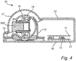
- FIGs 3 and 4 illustrate a camera 20 with the above discussed part 1 inside a housing comprising a cover 22 and a base plate 30.
- the camera cover 22 is disassembled from the base plate 30.
- the camera cover 22 is assembled to the base plate 30.
- the camera cover 22 comprises a window 21, and is designed to be fastened to the base plate 30 such that the camera part 1 can receive light through the window 21.
- the window 21 may be dome-shaped.
- a first PCB 13 is mounted under a PCB cover 11.
- the first PCB 13 and the PCB cover 11 are mounted with screws at a first mount point 12.
- the first PCB 13 may hold electronics, such as processors, memory chips, sensors of different kinds or other kinds of electronics.
- Rivets or other fastening means may be used instead of screws for the mount points 12.
- the part 1 of the camera 20 is supported in a front chassis part 18 and a rear chassis part 19 which principally enclose the mount holder 350 along with the lens array 600.
- the lens array 600 is partially visible, protruding through the front chassis part 18.
- the front chassis part 18 and the rear chassis part 19 are placed in a swivel mount 15.
- the swivel mount is arranged to provide the camera with pan and tilt functions for installation purposes.
- the swivel mount 15 is mounted on the base plate 30 by way of screws, at a second mount point 14. Again, other fastening means than screws may be used.
- the base plate 30 and camera cover 22 may be made from metal or polymer materials. Polymer materials are advantageous as they may be efficiently manufactured and weather resistant.
Landscapes
- Physics & Mathematics (AREA)
- Engineering & Computer Science (AREA)
- General Physics & Mathematics (AREA)
- Multimedia (AREA)
- Signal Processing (AREA)
- Power Engineering (AREA)
- Electromagnetism (AREA)
- Aviation & Aerospace Engineering (AREA)
- Condensed Matter Physics & Semiconductors (AREA)
- Computer Hardware Design (AREA)
- Microelectronics & Electronic Packaging (AREA)
- Optics & Photonics (AREA)
- Studio Devices (AREA)
- Lens Barrels (AREA)
- Camera Bodies And Camera Details Or Accessories (AREA)
- Cameras Adapted For Combination With Other Photographic Or Optical Apparatuses (AREA)
Claims (15)
- Caméra comprenant :un porte-détecteur (100),un détecteur d'images (150) monté sur le porte-détecteur (100),un porte-support (350), etun support de lentilles (300) qui est apte à recevoir un assortiment de lentilles (600) et qui est monté sur le porte-support (350),le porte-détecteur (100) étant fixé au porte-support (350),un intervalle (500) ayant une extension le long d'un axe de la caméra qui est perpendiculaire au détecteur d'images et à une extension principale du porte-détecteur étant formé entre le porte-détecteur (100) et le support de lentilles (300),caractérisée en ce quele porte-détecteur (100) est pourvu d'une saillie conductrice thermique (200) pontant l'intervalle (500) et qui est en contact avec le support de lentilles (300) au niveau d'une interface (250) en permettant un mouvement relatif entre le support de lentilles (300) et la saillie conductrice thermique (200) le long de l'axe optique tout en maintenant un contact entre le support de lentilles (300) et la saillie conductrice thermique (200).
- Caméra selon la revendication 1, dans laquelle le porte-détecteur (100) est fixé par adhésif au porte-support (350).
- Caméra selon l'une quelconque des revendications 1 à 2, dans laquelle l'interface (250) comprend une première surface (301) sur le support de lentilles (300) tourné vers une seconde surface (202) sur la saillie conductrice thermique (200), les première et seconde surfaces (301, 202) ayant toutes deux une normale s'étendant perpendiculairement à l'axe optique.
- Caméra selon l'une quelconque des revendications 1 à 3, dans laquelle la saillie conductrice thermique (200) est positionnée au niveau d'une zone intermédiaire du porte-détecteur (100), la zone intermédiaire s'étendant autour du détecteur d'images (150) et se trouvant dans un périmètre du porte-détecteur (100).
- Caméra selon la revendication 4, dans laquelle la zone intermédiaire se trouve dans un périmètre défini par des points de fixation (400) entre le porte-détecteur et le porte-support (350).
- Caméra selon la revendication 4 ou 5, dans laquelle la saillie conductrice thermique (200) couvre au moins 50 % de la circonférence de la zone intermédiaire autour du détecteur d'images (150).
- Caméra selon l'une quelconque des revendications 3 à 6, dans laquelle la première surface de l'interface (250) forme une surface d'enveloppe extérieure circulaire (301) et la seconde surface de l'interface (250) forme une surface d'enveloppe intérieure circulaire (202).
- Caméra selon l'une quelconque des revendications 1 à 7, dans laquelle le porte-détecteur est un circuit imprimé (100).
- Caméra selon l'une quelconque des revendications 1 à 8, dans laquelle la saillie conductrice thermique (200) est formée d'un matériau conducteur thermique fixé au porte-détecteur (100).
- Caméra selon l'une quelconque des revendications 1 à 9, dans laquelle le support de lentilles (300) est composé d'un matériau conducteur thermique, de préférence un matériau métallique.
- Caméra selon l'une quelconque des revendications 1 à 10, comprenant en outre un assortiment de lentilles (600) comprenant un élément tubulaire supportant une ou plusieurs lentilles, l'élément tubulaire étant inséré dans le support de lentilles (300).
- Caméra selon la revendication 11, dans laquelle l'élément tubulaire de l'assortiment de lentilles (600) est composé d'un matériau conducteur thermique, de préférence un matériau métallique.
- Caméra selon l'une quelconque des revendications 1 à 12, dans laquelle le support de lentilles (300) comprend une section tubulaire apte à recevoir l'assortiment de lentilles (600).
- Caméra selon l'une quelconque des revendications 1 à 13, dans laquelle le porte-support (350) comprend une section tubulaire apte à recevoir le support de lentilles (300).
- Caméra selon l'une quelconque des revendications 1 à 14, dans laquelle le porte-support (350) est composé d'un matériau à base de polymère.
Priority Applications (6)
| Application Number | Priority Date | Filing Date | Title |
|---|---|---|---|
| EP17195692.3A EP3471391B1 (fr) | 2017-10-10 | 2017-10-10 | Caméra |
| KR1020180101230A KR102180795B1 (ko) | 2017-10-10 | 2018-08-28 | 카메라 |
| CN201811138155.6A CN109660704B (zh) | 2017-10-10 | 2018-09-28 | 摄像机 |
| US16/150,791 US10692906B2 (en) | 2017-10-10 | 2018-10-03 | Camera |
| JP2018189377A JP6910998B2 (ja) | 2017-10-10 | 2018-10-04 | カメラ |
| TW107135153A TWI730254B (zh) | 2017-10-10 | 2018-10-05 | 攝影機 |
Applications Claiming Priority (1)
| Application Number | Priority Date | Filing Date | Title |
|---|---|---|---|
| EP17195692.3A EP3471391B1 (fr) | 2017-10-10 | 2017-10-10 | Caméra |
Publications (2)
| Publication Number | Publication Date |
|---|---|
| EP3471391A1 EP3471391A1 (fr) | 2019-04-17 |
| EP3471391B1 true EP3471391B1 (fr) | 2020-08-12 |
Family
ID=60083783
Family Applications (1)
| Application Number | Title | Priority Date | Filing Date |
|---|---|---|---|
| EP17195692.3A Active EP3471391B1 (fr) | 2017-10-10 | 2017-10-10 | Caméra |
Country Status (6)
| Country | Link |
|---|---|
| US (1) | US10692906B2 (fr) |
| EP (1) | EP3471391B1 (fr) |
| JP (1) | JP6910998B2 (fr) |
| KR (1) | KR102180795B1 (fr) |
| CN (1) | CN109660704B (fr) |
| TW (1) | TWI730254B (fr) |
Families Citing this family (1)
| Publication number | Priority date | Publication date | Assignee | Title |
|---|---|---|---|---|
| TWI753255B (zh) * | 2019-05-14 | 2022-01-21 | 群光電子股份有限公司 | 電子裝置及其鏡頭模組 |
Family Cites Families (30)
| Publication number | Priority date | Publication date | Assignee | Title |
|---|---|---|---|---|
| JP2001309216A (ja) * | 2000-04-24 | 2001-11-02 | Olympus Optical Co Ltd | 電子カメラ |
| TWI437301B (zh) * | 2006-02-03 | 2014-05-11 | Hitachi Maxell | Camera module |
| WO2008023894A1 (fr) * | 2006-08-22 | 2008-02-28 | Lg Innotek Co., Ltd | Module d'appareil-photo |
| JP2008211378A (ja) * | 2007-02-23 | 2008-09-11 | Auto Network Gijutsu Kenkyusho:Kk | 撮像装置 |
| US8647922B2 (en) * | 2007-11-08 | 2014-02-11 | Nanyang Technological University | Method of forming an interconnect on a semiconductor substrate |
| US7734171B2 (en) * | 2008-01-29 | 2010-06-08 | Autoliv Asp, Inc. | Snap-in retainer for a sensor system |
| JP2009246932A (ja) * | 2008-03-13 | 2009-10-22 | Olympus Imaging Corp | 撮影レンズユニット及びそれを用いた電子機器 |
| JP2009271405A (ja) * | 2008-05-09 | 2009-11-19 | Mitsumi Electric Co Ltd | カメラモジュール |
| CN101609836B (zh) * | 2008-06-19 | 2012-07-18 | 鸿富锦精密工业(深圳)有限公司 | 影像感测器模组及相机模组 |
| JP5037450B2 (ja) * | 2008-08-08 | 2012-09-26 | シャープ株式会社 | 表示素子・電子素子モジュールおよび電子情報機器 |
| JP2010145616A (ja) * | 2008-12-17 | 2010-07-01 | Nikon Corp | カメラボディ、レンズ鏡筒及びカメラシステム |
| CN101924081A (zh) | 2009-06-15 | 2010-12-22 | 鸿富锦精密工业(深圳)有限公司 | 影像感测器封装体及影像感测器模组 |
| JP2012029028A (ja) * | 2010-07-23 | 2012-02-09 | Panasonic Corp | センサパッケージ、撮像装置及び携帯電子機器 |
| WO2012015965A1 (fr) | 2010-07-27 | 2012-02-02 | Flir Systems, Inc. | Systèmes et procédés pour architecture de caméra infrarouge |
| GB2495887B (en) | 2010-08-09 | 2016-12-28 | Cambridge Mechatronics Ltd | Camera apparatus |
| CN102377949B (zh) * | 2010-08-13 | 2015-01-21 | 鸿富锦精密工业(深圳)有限公司 | 影像感测模组及相机模组 |
| US8947797B2 (en) * | 2010-11-15 | 2015-02-03 | DigitalOptics Corporation MEMS | Miniature MEMS actuator assemblies |
| DE102011011527A1 (de) | 2011-02-17 | 2012-08-23 | Conti Temic Microelectronic Gmbh | Kameramodul |
| KR101845089B1 (ko) * | 2011-11-23 | 2018-04-03 | 엘지이노텍 주식회사 | 카메라 모듈 |
| CN102854714A (zh) | 2012-08-16 | 2013-01-02 | 浙江宇视科技有限公司 | 一种变焦摄像机散热装置 |
| JP5488852B1 (ja) * | 2012-10-31 | 2014-05-14 | ミツミ電機株式会社 | レンズホルダ駆動装置及び携帯機器 |
| US20140168507A1 (en) * | 2012-12-17 | 2014-06-19 | Integrated Micro-Electronics, Inc. | Camera Module With Enhanced Heat Dissipation |
| KR101391176B1 (ko) * | 2013-04-29 | 2014-05-07 | 주식회사 뷰웍스 | 영상촬영장치 |
| CN105431775B (zh) * | 2013-07-29 | 2019-09-10 | Lg伊诺特有限公司 | 摄像机模块 |
| US10054757B2 (en) * | 2013-09-03 | 2018-08-21 | Veoneer Sweden Ab | Camera module for a motor vehicle and method of mounting a camera module |
| US9429750B2 (en) * | 2013-09-12 | 2016-08-30 | Sunming Technologies (Hk) Limited | Dust-free lens driving apparatus |
| DE102014212016A1 (de) * | 2014-06-23 | 2015-12-24 | Robert Bosch Gmbh | Kamera, insbesondere in einem Fahrzeug einsetzbar, sowie ein Verfahren zum Herstellen einer derartigen Kamera |
| JP6638151B2 (ja) | 2014-07-04 | 2020-01-29 | 日本電産コパル株式会社 | 撮像装置 |
| CN205179197U (zh) * | 2015-11-23 | 2016-04-20 | 深圳市大疆创新科技有限公司 | 影像撷取模组及航拍飞行器 |
| CN205142363U (zh) * | 2015-12-04 | 2016-04-06 | 苏州中德宏泰电子科技股份有限公司 | 一种摄像组件 |
-
2017
- 2017-10-10 EP EP17195692.3A patent/EP3471391B1/fr active Active
-
2018
- 2018-08-28 KR KR1020180101230A patent/KR102180795B1/ko active IP Right Grant
- 2018-09-28 CN CN201811138155.6A patent/CN109660704B/zh active Active
- 2018-10-03 US US16/150,791 patent/US10692906B2/en active Active
- 2018-10-04 JP JP2018189377A patent/JP6910998B2/ja active Active
- 2018-10-05 TW TW107135153A patent/TWI730254B/zh active
Non-Patent Citations (1)
| Title |
|---|
| None * |
Also Published As
| Publication number | Publication date |
|---|---|
| KR102180795B1 (ko) | 2020-11-19 |
| JP2019091016A (ja) | 2019-06-13 |
| CN109660704A (zh) | 2019-04-19 |
| US20190109166A1 (en) | 2019-04-11 |
| TWI730254B (zh) | 2021-06-11 |
| CN109660704B (zh) | 2021-06-25 |
| TW201925897A (zh) | 2019-07-01 |
| JP6910998B2 (ja) | 2021-07-28 |
| KR20190040447A (ko) | 2019-04-18 |
| US10692906B2 (en) | 2020-06-23 |
| EP3471391A1 (fr) | 2019-04-17 |
Similar Documents
| Publication | Publication Date | Title |
|---|---|---|
| CN100409668C (zh) | 摄像单元和摄像装置 | |
| CN107395931B (zh) | 用于电子设备的承载框架和电路板 | |
| US7329869B2 (en) | Camera system | |
| US8025950B2 (en) | Sensor-securing apparatus and camera module | |
| KR101455124B1 (ko) | 촬상 센서 패키지를 구비한 촬상장치 | |
| EP2981078B1 (fr) | Caméra à plusieurs capteurs à substrat portant un circuit ouvert | |
| JP2008211378A (ja) | 撮像装置 | |
| TWI698009B (zh) | 感光晶片封裝模組及其形成方法 | |
| JP2008219704A (ja) | 半導体装置 | |
| CN106537244A (zh) | 拍摄装置 | |
| US20130076975A1 (en) | Imaging device | |
| EP3471391B1 (fr) | Caméra | |
| JP5203318B2 (ja) | 撮像モジュールおよびその製造方法 | |
| JP6777422B2 (ja) | 撮像装置 | |
| JP2012083556A (ja) | カメラモジュール | |
| JP2007194272A (ja) | 撮像モジュール | |
| US20230232091A1 (en) | Image pickup apparatus | |
| JP2019192813A (ja) | 電子機器及び電子機器の製造方法 | |
| KR100930778B1 (ko) | 카메라 모듈 및 그 제조 방법 | |
| WO2022021150A1 (fr) | Viseur électronique et dispositif photographique | |
| JP7382271B2 (ja) | 撮像装置 | |
| JP2018189667A (ja) | 撮像装置 | |
| US11363172B1 (en) | Camera enclosure for thermal management | |
| JP2020174321A (ja) | 撮像装置 | |
| JP3606534B2 (ja) | 固体撮像装置 |
Legal Events
| Date | Code | Title | Description |
|---|---|---|---|
| PUAI | Public reference made under article 153(3) epc to a published international application that has entered the european phase |
Free format text: ORIGINAL CODE: 0009012 |
|
| STAA | Information on the status of an ep patent application or granted ep patent |
Free format text: STATUS: REQUEST FOR EXAMINATION WAS MADE |
|
| 17P | Request for examination filed |
Effective date: 20180530 |
|
| AK | Designated contracting states |
Kind code of ref document: A1 Designated state(s): AL AT BE BG CH CY CZ DE DK EE ES FI FR GB GR HR HU IE IS IT LI LT LU LV MC MK MT NL NO PL PT RO RS SE SI SK SM TR |
|
| AX | Request for extension of the european patent |
Extension state: BA ME |
|
| GRAP | Despatch of communication of intention to grant a patent |
Free format text: ORIGINAL CODE: EPIDOSNIGR1 |
|
| STAA | Information on the status of an ep patent application or granted ep patent |
Free format text: STATUS: GRANT OF PATENT IS INTENDED |
|
| INTG | Intention to grant announced |
Effective date: 20200528 |
|
| RIN1 | Information on inventor provided before grant (corrected) |
Inventor name: IDE, HIROYUKI |
|
| GRAS | Grant fee paid |
Free format text: ORIGINAL CODE: EPIDOSNIGR3 |
|
| GRAA | (expected) grant |
Free format text: ORIGINAL CODE: 0009210 |
|
| STAA | Information on the status of an ep patent application or granted ep patent |
Free format text: STATUS: THE PATENT HAS BEEN GRANTED |
|
| AK | Designated contracting states |
Kind code of ref document: B1 Designated state(s): AL AT BE BG CH CY CZ DE DK EE ES FI FR GB GR HR HU IE IS IT LI LT LU LV MC MK MT NL NO PL PT RO RS SE SI SK SM TR |
|
| REG | Reference to a national code |
Ref country code: CH Ref legal event code: EP |
|
| REG | Reference to a national code |
Ref country code: IE Ref legal event code: FG4D |
|
| REG | Reference to a national code |
Ref country code: DE Ref legal event code: R096 Ref document number: 602017021458 Country of ref document: DE |
|
| REG | Reference to a national code |
Ref country code: AT Ref legal event code: REF Ref document number: 1302718 Country of ref document: AT Kind code of ref document: T Effective date: 20200915 |
|
| REG | Reference to a national code |
Ref country code: SE Ref legal event code: TRGR |
|
| REG | Reference to a national code |
Ref country code: LT Ref legal event code: MG4D |
|
| REG | Reference to a national code |
Ref country code: NL Ref legal event code: MP Effective date: 20200812 |
|
| PG25 | Lapsed in a contracting state [announced via postgrant information from national office to epo] |
Ref country code: BG Free format text: LAPSE BECAUSE OF FAILURE TO SUBMIT A TRANSLATION OF THE DESCRIPTION OR TO PAY THE FEE WITHIN THE PRESCRIBED TIME-LIMIT Effective date: 20201112 Ref country code: LT Free format text: LAPSE BECAUSE OF FAILURE TO SUBMIT A TRANSLATION OF THE DESCRIPTION OR TO PAY THE FEE WITHIN THE PRESCRIBED TIME-LIMIT Effective date: 20200812 Ref country code: HR Free format text: LAPSE BECAUSE OF FAILURE TO SUBMIT A TRANSLATION OF THE DESCRIPTION OR TO PAY THE FEE WITHIN THE PRESCRIBED TIME-LIMIT Effective date: 20200812 Ref country code: NO Free format text: LAPSE BECAUSE OF FAILURE TO SUBMIT A TRANSLATION OF THE DESCRIPTION OR TO PAY THE FEE WITHIN THE PRESCRIBED TIME-LIMIT Effective date: 20201112 Ref country code: GR Free format text: LAPSE BECAUSE OF FAILURE TO SUBMIT A TRANSLATION OF THE DESCRIPTION OR TO PAY THE FEE WITHIN THE PRESCRIBED TIME-LIMIT Effective date: 20201113 Ref country code: FI Free format text: LAPSE BECAUSE OF FAILURE TO SUBMIT A TRANSLATION OF THE DESCRIPTION OR TO PAY THE FEE WITHIN THE PRESCRIBED TIME-LIMIT Effective date: 20200812 |
|
| REG | Reference to a national code |
Ref country code: AT Ref legal event code: MK05 Ref document number: 1302718 Country of ref document: AT Kind code of ref document: T Effective date: 20200812 |
|
| PG25 | Lapsed in a contracting state [announced via postgrant information from national office to epo] |
Ref country code: RS Free format text: LAPSE BECAUSE OF FAILURE TO SUBMIT A TRANSLATION OF THE DESCRIPTION OR TO PAY THE FEE WITHIN THE PRESCRIBED TIME-LIMIT Effective date: 20200812 Ref country code: PL Free format text: LAPSE BECAUSE OF FAILURE TO SUBMIT A TRANSLATION OF THE DESCRIPTION OR TO PAY THE FEE WITHIN THE PRESCRIBED TIME-LIMIT Effective date: 20200812 Ref country code: NL Free format text: LAPSE BECAUSE OF FAILURE TO SUBMIT A TRANSLATION OF THE DESCRIPTION OR TO PAY THE FEE WITHIN THE PRESCRIBED TIME-LIMIT Effective date: 20200812 Ref country code: LV Free format text: LAPSE BECAUSE OF FAILURE TO SUBMIT A TRANSLATION OF THE DESCRIPTION OR TO PAY THE FEE WITHIN THE PRESCRIBED TIME-LIMIT Effective date: 20200812 Ref country code: IS Free format text: LAPSE BECAUSE OF FAILURE TO SUBMIT A TRANSLATION OF THE DESCRIPTION OR TO PAY THE FEE WITHIN THE PRESCRIBED TIME-LIMIT Effective date: 20201212 |
|
| RAP2 | Party data changed (patent owner data changed or rights of a patent transferred) |
Owner name: AXIS AB |
|
| PG25 | Lapsed in a contracting state [announced via postgrant information from national office to epo] |
Ref country code: DK Free format text: LAPSE BECAUSE OF FAILURE TO SUBMIT A TRANSLATION OF THE DESCRIPTION OR TO PAY THE FEE WITHIN THE PRESCRIBED TIME-LIMIT Effective date: 20200812 Ref country code: CZ Free format text: LAPSE BECAUSE OF FAILURE TO SUBMIT A TRANSLATION OF THE DESCRIPTION OR TO PAY THE FEE WITHIN THE PRESCRIBED TIME-LIMIT Effective date: 20200812 Ref country code: RO Free format text: LAPSE BECAUSE OF FAILURE TO SUBMIT A TRANSLATION OF THE DESCRIPTION OR TO PAY THE FEE WITHIN THE PRESCRIBED TIME-LIMIT Effective date: 20200812 Ref country code: SM Free format text: LAPSE BECAUSE OF FAILURE TO SUBMIT A TRANSLATION OF THE DESCRIPTION OR TO PAY THE FEE WITHIN THE PRESCRIBED TIME-LIMIT Effective date: 20200812 Ref country code: EE Free format text: LAPSE BECAUSE OF FAILURE TO SUBMIT A TRANSLATION OF THE DESCRIPTION OR TO PAY THE FEE WITHIN THE PRESCRIBED TIME-LIMIT Effective date: 20200812 |
|
| REG | Reference to a national code |
Ref country code: DE Ref legal event code: R097 Ref document number: 602017021458 Country of ref document: DE |
|
| PG25 | Lapsed in a contracting state [announced via postgrant information from national office to epo] |
Ref country code: AT Free format text: LAPSE BECAUSE OF FAILURE TO SUBMIT A TRANSLATION OF THE DESCRIPTION OR TO PAY THE FEE WITHIN THE PRESCRIBED TIME-LIMIT Effective date: 20200812 Ref country code: AL Free format text: LAPSE BECAUSE OF FAILURE TO SUBMIT A TRANSLATION OF THE DESCRIPTION OR TO PAY THE FEE WITHIN THE PRESCRIBED TIME-LIMIT Effective date: 20200812 Ref country code: ES Free format text: LAPSE BECAUSE OF FAILURE TO SUBMIT A TRANSLATION OF THE DESCRIPTION OR TO PAY THE FEE WITHIN THE PRESCRIBED TIME-LIMIT Effective date: 20200812 |
|
| REG | Reference to a national code |
Ref country code: CH Ref legal event code: PL |
|
| PLBE | No opposition filed within time limit |
Free format text: ORIGINAL CODE: 0009261 |
|
| STAA | Information on the status of an ep patent application or granted ep patent |
Free format text: STATUS: NO OPPOSITION FILED WITHIN TIME LIMIT |
|
| PG25 | Lapsed in a contracting state [announced via postgrant information from national office to epo] |
Ref country code: MC Free format text: LAPSE BECAUSE OF FAILURE TO SUBMIT A TRANSLATION OF THE DESCRIPTION OR TO PAY THE FEE WITHIN THE PRESCRIBED TIME-LIMIT Effective date: 20200812 Ref country code: LU Free format text: LAPSE BECAUSE OF NON-PAYMENT OF DUE FEES Effective date: 20201010 Ref country code: SK Free format text: LAPSE BECAUSE OF FAILURE TO SUBMIT A TRANSLATION OF THE DESCRIPTION OR TO PAY THE FEE WITHIN THE PRESCRIBED TIME-LIMIT Effective date: 20200812 |
|
| REG | Reference to a national code |
Ref country code: BE Ref legal event code: MM Effective date: 20201031 |
|
| 26N | No opposition filed |
Effective date: 20210514 |
|
| PG25 | Lapsed in a contracting state [announced via postgrant information from national office to epo] |
Ref country code: IT Free format text: LAPSE BECAUSE OF FAILURE TO SUBMIT A TRANSLATION OF THE DESCRIPTION OR TO PAY THE FEE WITHIN THE PRESCRIBED TIME-LIMIT Effective date: 20200812 |
|
| PG25 | Lapsed in a contracting state [announced via postgrant information from national office to epo] |
Ref country code: SI Free format text: LAPSE BECAUSE OF FAILURE TO SUBMIT A TRANSLATION OF THE DESCRIPTION OR TO PAY THE FEE WITHIN THE PRESCRIBED TIME-LIMIT Effective date: 20200812 Ref country code: LI Free format text: LAPSE BECAUSE OF NON-PAYMENT OF DUE FEES Effective date: 20201031 Ref country code: BE Free format text: LAPSE BECAUSE OF NON-PAYMENT OF DUE FEES Effective date: 20201031 Ref country code: CH Free format text: LAPSE BECAUSE OF NON-PAYMENT OF DUE FEES Effective date: 20201031 |
|
| PG25 | Lapsed in a contracting state [announced via postgrant information from national office to epo] |
Ref country code: IE Free format text: LAPSE BECAUSE OF NON-PAYMENT OF DUE FEES Effective date: 20201010 |
|
| PG25 | Lapsed in a contracting state [announced via postgrant information from national office to epo] |
Ref country code: TR Free format text: LAPSE BECAUSE OF FAILURE TO SUBMIT A TRANSLATION OF THE DESCRIPTION OR TO PAY THE FEE WITHIN THE PRESCRIBED TIME-LIMIT Effective date: 20200812 Ref country code: MT Free format text: LAPSE BECAUSE OF FAILURE TO SUBMIT A TRANSLATION OF THE DESCRIPTION OR TO PAY THE FEE WITHIN THE PRESCRIBED TIME-LIMIT Effective date: 20200812 Ref country code: CY Free format text: LAPSE BECAUSE OF FAILURE TO SUBMIT A TRANSLATION OF THE DESCRIPTION OR TO PAY THE FEE WITHIN THE PRESCRIBED TIME-LIMIT Effective date: 20200812 |
|
| PG25 | Lapsed in a contracting state [announced via postgrant information from national office to epo] |
Ref country code: MK Free format text: LAPSE BECAUSE OF FAILURE TO SUBMIT A TRANSLATION OF THE DESCRIPTION OR TO PAY THE FEE WITHIN THE PRESCRIBED TIME-LIMIT Effective date: 20200812 |
|
| PG25 | Lapsed in a contracting state [announced via postgrant information from national office to epo] |
Ref country code: PT Free format text: LAPSE BECAUSE OF FAILURE TO SUBMIT A TRANSLATION OF THE DESCRIPTION OR TO PAY THE FEE WITHIN THE PRESCRIBED TIME-LIMIT Effective date: 20200812 |
|
| REG | Reference to a national code |
Ref country code: DE Ref legal event code: R079 Ref document number: 602017021458 Country of ref document: DE Free format text: PREVIOUS MAIN CLASS: H04N0005225000 Ipc: H04N0023000000 |
|
| P01 | Opt-out of the competence of the unified patent court (upc) registered |
Effective date: 20230505 |
|
| PGFP | Annual fee paid to national office [announced via postgrant information from national office to epo] |
Ref country code: GB Payment date: 20230920 Year of fee payment: 7 |
|
| PGFP | Annual fee paid to national office [announced via postgrant information from national office to epo] |
Ref country code: SE Payment date: 20230922 Year of fee payment: 7 Ref country code: FR Payment date: 20230920 Year of fee payment: 7 |
|
| PGFP | Annual fee paid to national office [announced via postgrant information from national office to epo] |
Ref country code: DE Payment date: 20230920 Year of fee payment: 7 |