EP3463901B1 - Print element board, liquid ejection head, and liquid ejection apparatus - Google Patents
Print element board, liquid ejection head, and liquid ejection apparatus Download PDFInfo
- Publication number
- EP3463901B1 EP3463901B1 EP17729562.3A EP17729562A EP3463901B1 EP 3463901 B1 EP3463901 B1 EP 3463901B1 EP 17729562 A EP17729562 A EP 17729562A EP 3463901 B1 EP3463901 B1 EP 3463901B1
- Authority
- EP
- European Patent Office
- Prior art keywords
- peak
- terminals
- print element
- element board
- liquid
- Prior art date
- Legal status (The legal status is an assumption and is not a legal conclusion. Google has not performed a legal analysis and makes no representation as to the accuracy of the status listed.)
- Active
Links
Images


Classifications
-
- B—PERFORMING OPERATIONS; TRANSPORTING
- B41—PRINTING; LINING MACHINES; TYPEWRITERS; STAMPS
- B41J—TYPEWRITERS; SELECTIVE PRINTING MECHANISMS, i.e. MECHANISMS PRINTING OTHERWISE THAN FROM A FORME; CORRECTION OF TYPOGRAPHICAL ERRORS
- B41J25/00—Actions or mechanisms not otherwise provided for
- B41J25/34—Bodily-changeable print heads or carriages
-
- B—PERFORMING OPERATIONS; TRANSPORTING
- B41—PRINTING; LINING MACHINES; TYPEWRITERS; STAMPS
- B41J—TYPEWRITERS; SELECTIVE PRINTING MECHANISMS, i.e. MECHANISMS PRINTING OTHERWISE THAN FROM A FORME; CORRECTION OF TYPOGRAPHICAL ERRORS
- B41J2/00—Typewriters or selective printing mechanisms characterised by the printing or marking process for which they are designed
- B41J2/005—Typewriters or selective printing mechanisms characterised by the printing or marking process for which they are designed characterised by bringing liquid or particles selectively into contact with a printing material
- B41J2/01—Ink jet
- B41J2/135—Nozzles
- B41J2/14—Structure thereof only for on-demand ink jet heads
- B41J2/14016—Structure of bubble jet print heads
- B41J2/14072—Electrical connections, e.g. details on electrodes, connecting the chip to the outside...
-
- B—PERFORMING OPERATIONS; TRANSPORTING
- B41—PRINTING; LINING MACHINES; TYPEWRITERS; STAMPS
- B41J—TYPEWRITERS; SELECTIVE PRINTING MECHANISMS, i.e. MECHANISMS PRINTING OTHERWISE THAN FROM A FORME; CORRECTION OF TYPOGRAPHICAL ERRORS
- B41J2/00—Typewriters or selective printing mechanisms characterised by the printing or marking process for which they are designed
- B41J2/005—Typewriters or selective printing mechanisms characterised by the printing or marking process for which they are designed characterised by bringing liquid or particles selectively into contact with a printing material
- B41J2/01—Ink jet
- B41J2/015—Ink jet characterised by the jet generation process
- B41J2/04—Ink jet characterised by the jet generation process generating single droplets or particles on demand
- B41J2/045—Ink jet characterised by the jet generation process generating single droplets or particles on demand by pressure, e.g. electromechanical transducers
- B41J2/04501—Control methods or devices therefor, e.g. driver circuits, control circuits
- B41J2/0458—Control methods or devices therefor, e.g. driver circuits, control circuits controlling heads based on heating elements forming bubbles
-
- B—PERFORMING OPERATIONS; TRANSPORTING
- B41—PRINTING; LINING MACHINES; TYPEWRITERS; STAMPS
- B41J—TYPEWRITERS; SELECTIVE PRINTING MECHANISMS, i.e. MECHANISMS PRINTING OTHERWISE THAN FROM A FORME; CORRECTION OF TYPOGRAPHICAL ERRORS
- B41J2/00—Typewriters or selective printing mechanisms characterised by the printing or marking process for which they are designed
- B41J2/005—Typewriters or selective printing mechanisms characterised by the printing or marking process for which they are designed characterised by bringing liquid or particles selectively into contact with a printing material
- B41J2/01—Ink jet
- B41J2/135—Nozzles
- B41J2/145—Arrangement thereof
- B41J2/155—Arrangement thereof for line printing
-
- B—PERFORMING OPERATIONS; TRANSPORTING
- B41—PRINTING; LINING MACHINES; TYPEWRITERS; STAMPS
- B41J—TYPEWRITERS; SELECTIVE PRINTING MECHANISMS, i.e. MECHANISMS PRINTING OTHERWISE THAN FROM A FORME; CORRECTION OF TYPOGRAPHICAL ERRORS
- B41J2202/00—Embodiments of or processes related to ink-jet or thermal heads
- B41J2202/01—Embodiments of or processes related to ink-jet heads
- B41J2202/20—Modules
Definitions
- the invention relates to a print element board for recording, a liquid ejection head provided with a print element board, and a liquid ejection apparatus.
- a liquid ejection head includes a print element board provided with a printing element which generates energy for ejecting a liquid, and a wiring substrate for electrically connecting the print element board and a main body of the liquid ejection apparatus.
- the print element board includes a terminal and is electrically connected with the wiring substrate via the terminal.
- a printing element is driven based on a signal input from a control circuit of the main body of the liquid ejection apparatus via the wiring substrate, and a liquid is ejected, whereby an image is recorded.
- U.S. Patent. No. 7407262 discloses a configuration in which terminals are arranged along a side of a print element board.
- a print element board of which principal surface is rectangular in shape a print element board of which principal surface is substantially parallelogrammatic in shape as described in Japanese Patent Laid-Open No. 2015-174385 is proposed.
- Another example printhead with a parallelogrammatic print element board is known from US 2015/328894 A1 .
- an angle at a first end of a side which forms a surface is smaller than an angle at a second end of the side as in a print element board of which surface is substantially parallelogrammatic in shape, the following issue may arise.
- chips and cracks may be produced with high possibility at a first end with a relatively smaller angle near a portion including the first end than a second end with a relatively larger angle. Therefore, if terminals are provided near a first end with a small angle, an electrical failure, such as disconnection of wires extending from these terminals, may be caused, and electric reliability of the print element board may be impaired.
- the angle is an acute angle, a possibility that chips and cracks may be produced near the angle is increased.
- the invention reduces a decrease in electric reliability in a print element board in which an angle at a peak at a first end of a side which forms a surface of the print element board is smaller than an angle at a peak of a second end of the side.
- a print element board of the invention is defined according to claim 1.
- the embodiments of the invention employ a thermal process in which heating elements are used as recording elements, and air bubbles are generated to eject a liquid.
- a print element board employing a piezoelectric process or other various types of liquids ejecting processes may also be applied to the invention.
- the invention is applicable also to a print element board of an industrial recording apparatus for manufacturing biochip, printing electronic circuits, and resist coating for forming a circuit pattern of a semiconductor wafer, for example.
- the present embodiment is a linear head having a length corresponding to a width of a recording medium
- the invention is applicable also to a serial liquid ejection head which records on a recording medium while moving the head.
- An exemplary serial liquid ejection head includes both a print element board for black ink and a print element board for color ink.
- FIG. 1 illustrates a schematic structure of the recording apparatus 1000.
- the recording apparatus 1000 includes a conveyance unit 1 which conveys a recording medium 2, and a linear liquid ejection head 3 disposed to substantially perpendicularly cross a conveying direction of the recording medium 2.
- the recording apparatus 1000 is a linear recording apparatus which continuously records on the recording medium 2 in one pass, while conveying a plurality of recording media 2 continuously or intermittently.
- the recording medium 2 is not limited to a cut sheet, but may be continuous rolled paper.
- the liquid ejection head 3 is capable of performing full color printing with cyan, magenta, yellow, and black (CMYK) ink.
- the liquid ejection head 3 is electrically connected with a control unit of the recording apparatus 1000 for transmitting power and ejection control signals to the liquid ejection head 3.
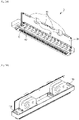
- Figs. 2A and 2B are perspective views of the liquid ejection head 3 according to the present embodiment.
- the liquid ejection head 3 is a linear liquid ejection head in which 15 print element boards 10 are arranged linearly in sequence (in-line). Each print element board 10 is capable of ejecting four (CMYK) colors of ink.
- the liquid ejection head 3 includes the print element boards 10, flexible wiring substrates 40, and an electric wiring board 90.
- the electric wiring board 90 includes signal input terminals 91 and power supply terminals 92.
- the signal input terminals 91 and the power supply terminals 92 are electrically connected with the control unit of the recording apparatus 1000, and ejection driving signals and power necessary for the ejection are supplied to the print element boards 10 via these terminals.
- liquid connecting portions 130 provided at both ends of the liquid ejection head 3 are connected with a liquid supply system of the recording apparatus 1000. Therefore, ink of four (CMYK) colors is supplied to the liquid ejection head 3 from the supply system of the recording apparatus 1000, and ink passed inside of the liquid ejection head 3 is collected to the supply system of the recording apparatus 1000. Thus, ink of each color can be circulated through paths in the recording apparatus 1000 and paths in the liquid ejection head 3.
- CMYK ink of four
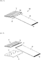
- Fig. 3A is a perspective view and Fig. 3B is an exploded view of the ejection module 200.
- the ejection module 200 includes a print element board 10, a flexible wiring substrate 40, and a support member 30 which supports the print element board 10 and the flexible wiring substrate 40.
- the print element board 10 and the flexible wiring substrate 40 are bonded on the support member 30.
- the support member 30 is a support which supports the print element board 10, and also is a flow path member capable of supplying a liquid to the print element board 10 via liquid communication ports 31.
- a plurality of ejection modules are arranged in the liquid ejection head 3 of the present embodiment.
- Terminals 16 provided in the print element board 10 and terminals 41 provided in the flexible wiring substrate 40 are electrically connected by wire bonding. An electrical connection portion formed by these terminals 16 and 41 and wires is covered with a sealing member 120. Terminals 42 of the flexible wiring substrate 40 provided on the opposite side of the terminals 41 connected with the print element board 10 are electrically connected with connection terminals of the electric wiring board 90.
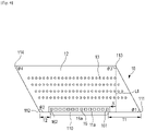
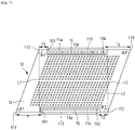
- Fig. 4 is a plan view of the print element board 10 seen from a side on which ejection ports 13 are provided.
- Fig. 5 is a perspective view illustrating a cross section in a direction perpendicularly crossing ejection port arrays of the print element board 10 of Fig. 4 .
- the print element board 10 is constituted by a substrate 11 including a silicon substrate and an ejection port forming member 12 formed by photosensitive resin which are laminated.
- a lid member 20 is joined to a back side of the substrate 11.
- Four ejection port arrays in which the ejection ports 13 are arranged are provided in the ejection port forming member 12.
- Printing elements 15 are provided on a surface 11a of the substrate 11 which constitutes the print element board 10 corresponding to the ejection ports 13, and four recording element arrays are provided corresponding to the four ejection port arrays.
- Grooves for forming liquid supply paths 18 and liquid collection paths 19 extending along the ejection port arrays are provided on the back side of the substrate 11, and the liquid supply paths 18 and the liquid collection paths 19 are formed by the substrate 11 and the lid member 20.
- a liquid (ink) which flows inside of the liquid supply paths 18 is supplied to pressure chambers 23 via supply ports 17a, generates energy used to eject the liquid by the printing element 15 when the printing element 15 is driven, whereby the supplied liquid is ejected.
- the liquid which flows inside of the liquid supply path 18 flows into the liquid collection paths 19 via the supply ports 17a, the pressure chambers 23, and collection ports 17b. With this liquid flow, thickened ink, air bubbles, foreign substance, etc. generated by evaporation from the ejection ports 13 can be collected to the liquid collection paths 19 in the ejection ports 13 and the pressure chambers 23 in which no ejection of the liquid is performed. Further, thickening of ink in the ejection ports 13 and the pressure chambers 23 may be prevented.
- the liquid collected to the liquid collection paths 19 passes openings 21 of the lid member 20 and liquid communication ports 31 ( Fig. 3B ) of the support member 30, and are collected to supply paths of the main body of the recording apparatus 1000 via the liquid connecting portions 130 ( Fig. 2B ).
- the liquid can be circulated between the pressure chambers 23 provided with the printing elements 15 thereinside and the main body of the recording apparatus 1000 which is outside of the pressure chambers 23.
- the surface 11a of the print element board 10 includes, near a side 110, an electric connection area 16a in which a plurality of terminals 16 are arranged along the side 110.
- no ejection port forming member 12 is provided in the electric connection area 16a of the substrate 11.
- the terminals 16 are electrically connected with the printing elements 15 via wires provided in the substrate 11.
- the terminals 16 are connected with the terminals 41 of the flexible wiring substrate 40.
- the printing elements 15 provided in the print element board 10 and the control circuit provided in the main body of the recording apparatus 1000 are electrically connected via the flexible wiring substrate 40 and the electric wiring board 90.
- the printing elements 15 are driven based on a signal input from the control circuit, generate heat, and eject the liquid.
- the print element board 10 is substantially parallelogrammatic in shape when seen from a side on which the ejection ports 13 are provided.
- An angle ⁇ 1 at a first peak 111 at a first end of the side 110 which forms the surface 11a of the print element board 10 (the substrate 11) is less than 90°
- an angle ⁇ 2 at a second peak 112 at a second end of the side 110 is greater than 90°.
- An angle ⁇ 4 at a fourth peak 114 located diagonally across the first peak 111 is less than 90°
- an angle ⁇ 3 at a third peak 113 located diagonally across the second peak 112 is greater than 90°. That is, the angle including the first peak 111 and the angle including the fourth peak 114 are acute angles, and the angle including the second peak 112 and the angle including the third peak 113 are obtuse angles.
- the shortest distance T1 between the first peak 111 and the electric connection area 16a is longer than the shortest distance T2 between the second peak 112 and the electric connection area 16a.
- the shortest distance T1 between the first peak 111 and the electric connection area 16a is also a distance between the first peak 111 and a first terminal 161 disposed closest to the first peak 111 among a plurality of terminals 16.
- the shortest distance T2 between the second peak 112 and the electric connection area 16a is also a distance between the second peak 112 and a second terminal 162 disposed closest to the second peak 112 among a plurality of terminals 16.
- the distance between the first end at which the inner angle is relatively smaller and the electric connection area 16a is set to be longer than a distance between the second end at which the inner angle is relatively larger and the electric connection area 16a.
- a distance from the first peak 111 which is the side of both ends of the side 110 on which chips tend to be produced to the electric connection area 16a can be kept unused. Since it is unnecessary to dispose the terminals 16 and wires extending from the terminals 16 near the first peak 111, even if chips and cracks are produced in the print element board 10 at the first peak 111 or near the first peak 111, a possibility of occurrence of disconnection of the wires extending from the terminals 16 can be reduced. Therefore, a decrease in electrical reliability of the print element board 10 can be prevented.
- the shortest distance between the first peak 111 and the electric connection area 16a and the shortest distance between the second peak 112 and the electric connection area 16a of the print element board 10 become shorter. Especially in this case, it is effective to set the shortest distance T1 between the first peak 111 and the electric connection area 16a to be longer than the shortest distance T2 between the second peak 112 and the electric connection area 16b as described above.
- the electric connection area 16a is desirably provided nearer to the second peak 112 than an imaginary line L1 which passes the third peak 113 located diagonally across the second peak 112 and perpendicularly crosses the side 110. That is, the first terminal 161 disposed closest to the first peak 111 is desirably provided nearer to an arrow X than the imaginary line L1. Therefore, since the first peak 111 and the electric connection area 16a can be separated from each other, electric reliability can be further increased.
- the surface 11a of the print element board 10 (the substrate 11) is parallelogrammatic in shape in the present embodiment, the invention is not limited to the same.
- An angle at the peak at the first end of the side which forms the surface 11a of the print element board 10 may desirably be smaller than an angle at the peak at the second end of the side.
- the invention is applicable also to a case where a print element board of trapezoid and polygon in shape is employed, for example.
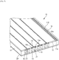
- Fig. 6A is a perspective view and Fig. 6B is an exploded view of the ejection module 200.
- a plurality of terminals 16 are disposed at both sides along ejection port arrays of a print element board 10 (each long side of the print element board 10), and two flexible wiring substrates 40 which are electrically connected with the terminals 16 are provided with respect to a single print element board 10. This is because twenty ejection port arrays, which are significantly greater in number than those of the first embodiment, are provided in the print element board 10.
- an object of the present embodiment if to control the longest distance from the terminals 16 to printing elements 15 provided corresponding to the ejection port arrays to be short, whereby a voltage drop caused in a wiring portion and signal transmission delay in the print element board 10 is to be reduced.
- Fig. 7 is a plan view of the print element board 10 seen from a side on which ejection ports 13 are provided. Twenty ejection port arrays are formed in the ejection port forming member 12 of the print element board 10.
- the print element board 10 is substantially parallelogrammatic in shape when seen from a side on which the ejection ports 13 are provided.
- An angle ⁇ 1 at a first peak 111 at a first end of the side 110 which forms the surface 11a of the print element board 10 (the substrate 11) is less than 90°
- an angle ⁇ 2 at a second peak 112 at a second end of the side 110 is greater than 90°.
- An angle ⁇ 4 at a fourth peak 114 located diagonally across the first peak 111 is less than 90°
- an angle ⁇ 3 at a third peak 113 located diagonally across the second peak 112 is greater than 90°.
- a surface 11a of the print element board 10 also has an electric connection area 16b in which a plurality of terminals 16 are arranged along a side 115 near the side 115 opposite to the side 110 besides an electric connection area 16a provided near the side 110.
- the shortest distance T1 between the first peak 111 and the electric connection area 16a is longer than the shortest distance T2 between the second peak 112 and the electric connection area 16a.
- the shortest distance T4 between a fourth peak 114 and the electric connection area 16b is longer than the shortest distance T3 between a third peak 113 and the electric connection area 16b.
- the shortest distance T1 is also a distance between the first peak 111 and a first terminal 161 disposed closest to the first peak 111 among a plurality of terminals 16 disposed in the electric connection area 16a.
- the shortest distance T2 is also a distance between the second peak 112 and a second terminal 162 disposed closest to the second peak 112 among a plurality of terminals 16 disposed in the electric connection area 16a.
- the shortest distance T3 is also a distance between the third peak 113 and a third terminal 163 disposed closest to the third peak 113 among a plurality of terminals 16 disposed in the another electric connection area 16b.
- the shortest distance T4 is also a distance between the fourth peak 114 and a fourth terminal 164 disposed closest to the fourth peak 114 among a plurality of terminals 16 disposed in the another electric connection area 16b.
- a distance from the first peak 111 which is the side of both ends of the side 110 on which chips tend to be produced to the electric connection area 16a can be provided, and a distance from the fourth peak 114 which is the side of both ends of the side 115 on which chips tend to be produced to the electric connection area 16b can be kept unused. Therefore, it is unnecessary to dispose the terminals 16 and wires extending from the terminals 16 near the first peak 111 and the fourth peak 114. Even if chips and cracks are produced in the print element board 10 at the first peak 111 or near the first peak 111, at the fourth peak 114 or near the fourth peak 114, a possibility of occurrence of disconnection of the wires extending from the terminals 16 can be reduced. Therefore, a decrease in electrical reliability of the print element board 10 can be prevented.
- the electric connection area 16a is desirably provided nearer to the second peak 112 than an imaginary line L1 which passes the third peak 113 located diagonally across the second peak 112 and perpendicularly crosses the side 110. That is, the first terminal 161 disposed closest to the first peak 111 is desirably provided nearer to the second peak 112 than the imaginary line L1. Similarly, the electric connection area 16b is desirably provided nearer to the third peak 113 than an imaginary line L2 which passes the second peak 112 located diagonally across the third peak 113 and perpendicularly crosses the side 115.
- the fourth terminal 164 disposed closest to the fourth peak 114 is desirably provided nearer to the third peak 113 than the imaginary line L2. Therefore, since the first peak 111 and the electric connection area 16a can be separated from each other, and the fourth peak 114 and the electric connection area 16b can be separated from each other, electric reliability can be further increased.
- a distance between a first end at which an inner angle is relatively smaller and the electric connection area 16 may desirably be set to be longer than a distance between a second end at which an inner angle is relatively larger and the electric connection area 16.
- the terminals 16 are electrically connected with terminals 41 provided in the flexible wiring substrates 40, and are covered with sealing members 120.
- the print element board 10 is affected by cure shrinkage or thermal expansion of the sealing members 120.
- the sealing members 120 are disposed at opposite sides 110 and 115 of the print element board 10, an influence of positional misalignment caused by cure shrinkage and thermal expansion of the sealing member 120 is offset and reduced.
- the print element board 10 is substantially parallelogrammatic in shape, since a bonding area between the print element board 10 and a support member 30 in a direction perpendicularly crossing the side 110 is smaller than other areas near the first peak 111 which is an acute angle side, bonding strength between the print element board 10 and the support member 30 is low. The same applies to an area near the fourth peak 114. Therefore, even if the sealing members 120 are disposed at opposite sides 110 and 115, if the sealing members 120 are disposed at the areas near the firs peak 111 and the fourth peak 114, positional misalignment may be caused in a direction in which the print element board 10 is rotated with force by contraction and expansion of the sealing members 120.
- the shortest distance T1 between the first peak 111 and the electric connection area 16a is longer than the shortest distance T2 between the second peak 112 and the electric connection area 16a. Further, the shortest distance T4 between the fourth peak 114 and the electric connection area 16b is longer than the shortest distance T3 between the third peak 113 and the electric connection area 16b. Accordingly, the shortest distance between the first peak 111 and the sealing member 120 which covers the electric connection area 16a is longer than the shortest distance between the second peak 112 and the sealing member 120 which covers the electric connection area 16a.
- the shortest distance between the fourth peak 114 and the sealing member 120 which covers the electric connection area 16b is longer than the shortest distance between the third peak 113 and the sealing member 120 which covers the electric connection area 16b. Therefore, since the first peak 111 and the sealing member 120 can be separated from each other, and the fourth peak 114 and the sealing member 120 can be separated from each other, occurrence of positional misalignment of the print element board 10 caused by contraction and expansion of the sealing members 120 can be prevented.
- the electric connection area 16a and the sealing member 120 covering the electric connection area 16a may desirably be disposed nearer to the second peak 112 than the imaginary line L1, and the electric connection area 16b and the sealing member 120 covering the electric connection area 16b may desirably be provided nearer to the third peak 113 than the imaginary line L2. Therefore, an area to be affected by contraction and expansion of the sealing members 120 is limited to a rectangular area constituted by the side 110, the side 115, the imaginary line L1, and the imaginary line L2 of the print element board 10.
- the sealing members 120 can be disposed substantially symmetrically on the side 110 and on the side 115, the same influence due to contraction and expansion of the sealing members 120 may be applied to the side 110 and the side 110, whereby occurrence of positional misalignment of the print element board 10 can be further prevented.
Landscapes
- Particle Formation And Scattering Control In Inkjet Printers (AREA)
Applications Claiming Priority (2)
| Application Number | Priority Date | Filing Date | Title |
|---|---|---|---|
| JP2016107911A JP6821331B2 (ja) | 2016-05-30 | 2016-05-30 | 記録素子基板、液体吐出ヘッド、及び液体吐出装置 |
| PCT/JP2017/019624 WO2017208978A1 (en) | 2016-05-30 | 2017-05-25 | Print element board, liquid ejection head, and liquid ejection apparatus |
Publications (2)
| Publication Number | Publication Date |
|---|---|
| EP3463901A1 EP3463901A1 (en) | 2019-04-10 |
| EP3463901B1 true EP3463901B1 (en) | 2022-05-25 |
Family
ID=59054161
Family Applications (1)
| Application Number | Title | Priority Date | Filing Date |
|---|---|---|---|
| EP17729562.3A Active EP3463901B1 (en) | 2016-05-30 | 2017-05-25 | Print element board, liquid ejection head, and liquid ejection apparatus |
Country Status (5)
| Country | Link |
|---|---|
| US (1) | US10933669B2 (enExample) |
| EP (1) | EP3463901B1 (enExample) |
| JP (1) | JP6821331B2 (enExample) |
| CN (1) | CN109311322B (enExample) |
| WO (1) | WO2017208978A1 (enExample) |
Families Citing this family (1)
| Publication number | Priority date | Publication date | Assignee | Title |
|---|---|---|---|---|
| JP7052640B2 (ja) * | 2018-08-24 | 2022-04-12 | ブラザー工業株式会社 | 液体吐出ヘッド |
Citations (1)
| Publication number | Priority date | Publication date | Assignee | Title |
|---|---|---|---|---|
| US20020021326A1 (en) * | 2000-07-10 | 2002-02-21 | Mineo Kaneko | Liquid discharge recording head and liquid discharge recording apparatus |
Family Cites Families (11)
| Publication number | Priority date | Publication date | Assignee | Title |
|---|---|---|---|---|
| JP3552004B2 (ja) * | 1996-09-24 | 2004-08-11 | セイコーエプソン株式会社 | インクジェット式ライン記録ヘッド、及び記録装置 |
| JPH10202876A (ja) * | 1997-01-23 | 1998-08-04 | Seiko Epson Corp | インクジェット式記録ヘッド |
| US7448734B2 (en) | 2004-01-21 | 2008-11-11 | Silverbrook Research Pty Ltd | Inkjet printer cartridge with pagewidth printhead |
| JP4616609B2 (ja) * | 2004-10-05 | 2011-01-19 | ブラザー工業株式会社 | インクジェットヘッド |
| US8118405B2 (en) * | 2008-12-18 | 2012-02-21 | Eastman Kodak Company | Buttable printhead module and pagewide printhead |
| WO2014203705A1 (ja) * | 2013-06-21 | 2014-12-24 | 京セラ株式会社 | 液体吐出ヘッドおよび記録装置 |
| JP6417684B2 (ja) | 2014-03-17 | 2018-11-07 | セイコーエプソン株式会社 | 液体噴射ヘッド及び液体噴射装置 |
| JP6659088B2 (ja) * | 2014-05-13 | 2020-03-04 | キヤノン株式会社 | 液体吐出ヘッド |
| JP6497902B2 (ja) * | 2014-11-21 | 2019-04-10 | キヤノン株式会社 | 記録ヘッド基板、記録ヘッド及び記録装置 |
| JP6976708B2 (ja) * | 2017-04-21 | 2021-12-08 | キヤノン株式会社 | 液体吐出ヘッド及びインクジェット記録装置 |
| US10479075B2 (en) * | 2017-05-09 | 2019-11-19 | Canon Kabushiki Kaisha | Print head substrate and method of manufacturing the same, and semiconductor substrate |
-
2016
- 2016-05-30 JP JP2016107911A patent/JP6821331B2/ja active Active
-
2017
- 2017-05-25 WO PCT/JP2017/019624 patent/WO2017208978A1/en not_active Ceased
- 2017-05-25 CN CN201780033181.XA patent/CN109311322B/zh active Active
- 2017-05-25 US US16/305,024 patent/US10933669B2/en active Active
- 2017-05-25 EP EP17729562.3A patent/EP3463901B1/en active Active
Patent Citations (1)
| Publication number | Priority date | Publication date | Assignee | Title |
|---|---|---|---|---|
| US20020021326A1 (en) * | 2000-07-10 | 2002-02-21 | Mineo Kaneko | Liquid discharge recording head and liquid discharge recording apparatus |
Also Published As
| Publication number | Publication date |
|---|---|
| US10933669B2 (en) | 2021-03-02 |
| JP2017213730A (ja) | 2017-12-07 |
| JP6821331B2 (ja) | 2021-01-27 |
| WO2017208978A1 (en) | 2017-12-07 |
| US20200316971A1 (en) | 2020-10-08 |
| CN109311322A (zh) | 2019-02-05 |
| EP3463901A1 (en) | 2019-04-10 |
| CN109311322B (zh) | 2020-07-28 |
Similar Documents
| Publication | Publication Date | Title |
|---|---|---|
| JP5656451B2 (ja) | 液体吐出ヘッド及び電気配線基板 | |
| US10603911B2 (en) | Printhead | |
| JP4604608B2 (ja) | 複合基板及びインクジェットプリンタ | |
| CN109130505B (zh) | 液体喷出头 | |
| US12420548B2 (en) | Liquid ejection head and liquid ejection apparatus | |
| EP3463901B1 (en) | Print element board, liquid ejection head, and liquid ejection apparatus | |
| KR20020068452A (ko) | 잉크젯 기록 장치 | |
| US11161351B2 (en) | Liquid ejection head | |
| US6869168B2 (en) | Liquid ejection print head | |
| US7797831B2 (en) | Method for manufacturing recording apparatus | |
| JP4561641B2 (ja) | インクジェットヘッドの製造方法 | |
| JP7778627B2 (ja) | 液体吐出ヘッド、及び液体吐出装置 | |
| JP7346148B2 (ja) | 液体吐出ヘッド | |
| JP6375973B2 (ja) | 液体吐出装置、及び、液体吐出装置の製造方法 | |
| JP2016034739A (ja) | 液体噴射ヘッドおよび液体噴射装置 | |
| US20230311500A1 (en) | Liquid ejection head and liquid ejection apparatus | |
| JP7056354B2 (ja) | 記録装置、配線部材及び配線部材の製造方法 | |
| JP4320619B2 (ja) | インクジェットヘッドの製造方法 | |
| CN120481457A (zh) | 液体喷射头 | |
| JP2023152238A (ja) | 液体吐出ヘッド及び液体吐出装置 | |
| JP2011253858A (ja) | 配線基板ユニット |
Legal Events
| Date | Code | Title | Description |
|---|---|---|---|
| STAA | Information on the status of an ep patent application or granted ep patent |
Free format text: STATUS: UNKNOWN |
|
| STAA | Information on the status of an ep patent application or granted ep patent |
Free format text: STATUS: THE INTERNATIONAL PUBLICATION HAS BEEN MADE |
|
| PUAI | Public reference made under article 153(3) epc to a published international application that has entered the european phase |
Free format text: ORIGINAL CODE: 0009012 |
|
| STAA | Information on the status of an ep patent application or granted ep patent |
Free format text: STATUS: REQUEST FOR EXAMINATION WAS MADE |
|
| 17P | Request for examination filed |
Effective date: 20190102 |
|
| AK | Designated contracting states |
Kind code of ref document: A1 Designated state(s): AL AT BE BG CH CY CZ DE DK EE ES FI FR GB GR HR HU IE IS IT LI LT LU LV MC MK MT NL NO PL PT RO RS SE SI SK SM TR |
|
| AX | Request for extension of the european patent |
Extension state: BA ME |
|
| DAV | Request for validation of the european patent (deleted) | ||
| DAX | Request for extension of the european patent (deleted) | ||
| STAA | Information on the status of an ep patent application or granted ep patent |
Free format text: STATUS: EXAMINATION IS IN PROGRESS |
|
| 17Q | First examination report despatched |
Effective date: 20200617 |
|
| GRAP | Despatch of communication of intention to grant a patent |
Free format text: ORIGINAL CODE: EPIDOSNIGR1 |
|
| STAA | Information on the status of an ep patent application or granted ep patent |
Free format text: STATUS: GRANT OF PATENT IS INTENDED |
|
| INTG | Intention to grant announced |
Effective date: 20211222 |
|
| GRAS | Grant fee paid |
Free format text: ORIGINAL CODE: EPIDOSNIGR3 |
|
| GRAA | (expected) grant |
Free format text: ORIGINAL CODE: 0009210 |
|
| STAA | Information on the status of an ep patent application or granted ep patent |
Free format text: STATUS: THE PATENT HAS BEEN GRANTED |
|
| AK | Designated contracting states |
Kind code of ref document: B1 Designated state(s): AL AT BE BG CH CY CZ DE DK EE ES FI FR GB GR HR HU IE IS IT LI LT LU LV MC MK MT NL NO PL PT RO RS SE SI SK SM TR |
|
| REG | Reference to a national code |
Ref country code: GB Ref legal event code: FG4D |
|
| REG | Reference to a national code |
Ref country code: CH Ref legal event code: EP |
|
| REG | Reference to a national code |
Ref country code: DE Ref legal event code: R096 Ref document number: 602017057813 Country of ref document: DE |
|
| REG | Reference to a national code |
Ref country code: AT Ref legal event code: REF Ref document number: 1494107 Country of ref document: AT Kind code of ref document: T Effective date: 20220615 |
|
| REG | Reference to a national code |
Ref country code: IE Ref legal event code: FG4D |
|
| REG | Reference to a national code |
Ref country code: LT Ref legal event code: MG9D |
|
| REG | Reference to a national code |
Ref country code: NL Ref legal event code: MP Effective date: 20220525 |
|
| REG | Reference to a national code |
Ref country code: AT Ref legal event code: MK05 Ref document number: 1494107 Country of ref document: AT Kind code of ref document: T Effective date: 20220525 |
|
| PG25 | Lapsed in a contracting state [announced via postgrant information from national office to epo] |
Ref country code: SE Free format text: LAPSE BECAUSE OF FAILURE TO SUBMIT A TRANSLATION OF THE DESCRIPTION OR TO PAY THE FEE WITHIN THE PRESCRIBED TIME-LIMIT Effective date: 20220525 Ref country code: PT Free format text: LAPSE BECAUSE OF FAILURE TO SUBMIT A TRANSLATION OF THE DESCRIPTION OR TO PAY THE FEE WITHIN THE PRESCRIBED TIME-LIMIT Effective date: 20220926 Ref country code: NO Free format text: LAPSE BECAUSE OF FAILURE TO SUBMIT A TRANSLATION OF THE DESCRIPTION OR TO PAY THE FEE WITHIN THE PRESCRIBED TIME-LIMIT Effective date: 20220825 Ref country code: NL Free format text: LAPSE BECAUSE OF FAILURE TO SUBMIT A TRANSLATION OF THE DESCRIPTION OR TO PAY THE FEE WITHIN THE PRESCRIBED TIME-LIMIT Effective date: 20220525 Ref country code: LT Free format text: LAPSE BECAUSE OF FAILURE TO SUBMIT A TRANSLATION OF THE DESCRIPTION OR TO PAY THE FEE WITHIN THE PRESCRIBED TIME-LIMIT Effective date: 20220525 Ref country code: HR Free format text: LAPSE BECAUSE OF FAILURE TO SUBMIT A TRANSLATION OF THE DESCRIPTION OR TO PAY THE FEE WITHIN THE PRESCRIBED TIME-LIMIT Effective date: 20220525 Ref country code: GR Free format text: LAPSE BECAUSE OF FAILURE TO SUBMIT A TRANSLATION OF THE DESCRIPTION OR TO PAY THE FEE WITHIN THE PRESCRIBED TIME-LIMIT Effective date: 20220826 Ref country code: FI Free format text: LAPSE BECAUSE OF FAILURE TO SUBMIT A TRANSLATION OF THE DESCRIPTION OR TO PAY THE FEE WITHIN THE PRESCRIBED TIME-LIMIT Effective date: 20220525 Ref country code: ES Free format text: LAPSE BECAUSE OF FAILURE TO SUBMIT A TRANSLATION OF THE DESCRIPTION OR TO PAY THE FEE WITHIN THE PRESCRIBED TIME-LIMIT Effective date: 20220525 Ref country code: BG Free format text: LAPSE BECAUSE OF FAILURE TO SUBMIT A TRANSLATION OF THE DESCRIPTION OR TO PAY THE FEE WITHIN THE PRESCRIBED TIME-LIMIT Effective date: 20220825 Ref country code: AT Free format text: LAPSE BECAUSE OF FAILURE TO SUBMIT A TRANSLATION OF THE DESCRIPTION OR TO PAY THE FEE WITHIN THE PRESCRIBED TIME-LIMIT Effective date: 20220525 |
|
| PG25 | Lapsed in a contracting state [announced via postgrant information from national office to epo] |
Ref country code: RS Free format text: LAPSE BECAUSE OF FAILURE TO SUBMIT A TRANSLATION OF THE DESCRIPTION OR TO PAY THE FEE WITHIN THE PRESCRIBED TIME-LIMIT Effective date: 20220525 Ref country code: PL Free format text: LAPSE BECAUSE OF FAILURE TO SUBMIT A TRANSLATION OF THE DESCRIPTION OR TO PAY THE FEE WITHIN THE PRESCRIBED TIME-LIMIT Effective date: 20220525 Ref country code: LV Free format text: LAPSE BECAUSE OF FAILURE TO SUBMIT A TRANSLATION OF THE DESCRIPTION OR TO PAY THE FEE WITHIN THE PRESCRIBED TIME-LIMIT Effective date: 20220525 Ref country code: IS Free format text: LAPSE BECAUSE OF FAILURE TO SUBMIT A TRANSLATION OF THE DESCRIPTION OR TO PAY THE FEE WITHIN THE PRESCRIBED TIME-LIMIT Effective date: 20220925 |
|
| REG | Reference to a national code |
Ref country code: CH Ref legal event code: PL |
|
| REG | Reference to a national code |
Ref country code: BE Ref legal event code: MM Effective date: 20220531 |
|
| PG25 | Lapsed in a contracting state [announced via postgrant information from national office to epo] |
Ref country code: SM Free format text: LAPSE BECAUSE OF FAILURE TO SUBMIT A TRANSLATION OF THE DESCRIPTION OR TO PAY THE FEE WITHIN THE PRESCRIBED TIME-LIMIT Effective date: 20220525 Ref country code: SK Free format text: LAPSE BECAUSE OF FAILURE TO SUBMIT A TRANSLATION OF THE DESCRIPTION OR TO PAY THE FEE WITHIN THE PRESCRIBED TIME-LIMIT Effective date: 20220525 Ref country code: RO Free format text: LAPSE BECAUSE OF FAILURE TO SUBMIT A TRANSLATION OF THE DESCRIPTION OR TO PAY THE FEE WITHIN THE PRESCRIBED TIME-LIMIT Effective date: 20220525 Ref country code: LU Free format text: LAPSE BECAUSE OF NON-PAYMENT OF DUE FEES Effective date: 20220525 Ref country code: LI Free format text: LAPSE BECAUSE OF NON-PAYMENT OF DUE FEES Effective date: 20220531 Ref country code: EE Free format text: LAPSE BECAUSE OF FAILURE TO SUBMIT A TRANSLATION OF THE DESCRIPTION OR TO PAY THE FEE WITHIN THE PRESCRIBED TIME-LIMIT Effective date: 20220525 Ref country code: DK Free format text: LAPSE BECAUSE OF FAILURE TO SUBMIT A TRANSLATION OF THE DESCRIPTION OR TO PAY THE FEE WITHIN THE PRESCRIBED TIME-LIMIT Effective date: 20220525 Ref country code: CZ Free format text: LAPSE BECAUSE OF FAILURE TO SUBMIT A TRANSLATION OF THE DESCRIPTION OR TO PAY THE FEE WITHIN THE PRESCRIBED TIME-LIMIT Effective date: 20220525 Ref country code: CH Free format text: LAPSE BECAUSE OF NON-PAYMENT OF DUE FEES Effective date: 20220531 |
|
| PG25 | Lapsed in a contracting state [announced via postgrant information from national office to epo] |
Ref country code: MC Free format text: LAPSE BECAUSE OF FAILURE TO SUBMIT A TRANSLATION OF THE DESCRIPTION OR TO PAY THE FEE WITHIN THE PRESCRIBED TIME-LIMIT Effective date: 20220525 |
|
| REG | Reference to a national code |
Ref country code: DE Ref legal event code: R097 Ref document number: 602017057813 Country of ref document: DE |
|
| PG25 | Lapsed in a contracting state [announced via postgrant information from national office to epo] |
Ref country code: AL Free format text: LAPSE BECAUSE OF FAILURE TO SUBMIT A TRANSLATION OF THE DESCRIPTION OR TO PAY THE FEE WITHIN THE PRESCRIBED TIME-LIMIT Effective date: 20220525 |
|
| PLBE | No opposition filed within time limit |
Free format text: ORIGINAL CODE: 0009261 |
|
| STAA | Information on the status of an ep patent application or granted ep patent |
Free format text: STATUS: NO OPPOSITION FILED WITHIN TIME LIMIT |
|
| PG25 | Lapsed in a contracting state [announced via postgrant information from national office to epo] |
Ref country code: IE Free format text: LAPSE BECAUSE OF NON-PAYMENT OF DUE FEES Effective date: 20220525 Ref country code: FR Free format text: LAPSE BECAUSE OF NON-PAYMENT OF DUE FEES Effective date: 20220725 |
|
| 26N | No opposition filed |
Effective date: 20230228 |
|
| PG25 | Lapsed in a contracting state [announced via postgrant information from national office to epo] |
Ref country code: SI Free format text: LAPSE BECAUSE OF FAILURE TO SUBMIT A TRANSLATION OF THE DESCRIPTION OR TO PAY THE FEE WITHIN THE PRESCRIBED TIME-LIMIT Effective date: 20220525 Ref country code: BE Free format text: LAPSE BECAUSE OF NON-PAYMENT OF DUE FEES Effective date: 20220531 |
|
| PG25 | Lapsed in a contracting state [announced via postgrant information from national office to epo] |
Ref country code: IT Free format text: LAPSE BECAUSE OF FAILURE TO SUBMIT A TRANSLATION OF THE DESCRIPTION OR TO PAY THE FEE WITHIN THE PRESCRIBED TIME-LIMIT Effective date: 20220525 |
|
| PG25 | Lapsed in a contracting state [announced via postgrant information from national office to epo] |
Ref country code: HU Free format text: LAPSE BECAUSE OF FAILURE TO SUBMIT A TRANSLATION OF THE DESCRIPTION OR TO PAY THE FEE WITHIN THE PRESCRIBED TIME-LIMIT; INVALID AB INITIO Effective date: 20170525 |
|
| PG25 | Lapsed in a contracting state [announced via postgrant information from national office to epo] |
Ref country code: MK Free format text: LAPSE BECAUSE OF FAILURE TO SUBMIT A TRANSLATION OF THE DESCRIPTION OR TO PAY THE FEE WITHIN THE PRESCRIBED TIME-LIMIT Effective date: 20220525 Ref country code: CY Free format text: LAPSE BECAUSE OF FAILURE TO SUBMIT A TRANSLATION OF THE DESCRIPTION OR TO PAY THE FEE WITHIN THE PRESCRIBED TIME-LIMIT Effective date: 20220525 |
|
| PG25 | Lapsed in a contracting state [announced via postgrant information from national office to epo] |
Ref country code: TR Free format text: LAPSE BECAUSE OF FAILURE TO SUBMIT A TRANSLATION OF THE DESCRIPTION OR TO PAY THE FEE WITHIN THE PRESCRIBED TIME-LIMIT Effective date: 20220525 |
|
| PG25 | Lapsed in a contracting state [announced via postgrant information from national office to epo] |
Ref country code: MT Free format text: LAPSE BECAUSE OF FAILURE TO SUBMIT A TRANSLATION OF THE DESCRIPTION OR TO PAY THE FEE WITHIN THE PRESCRIBED TIME-LIMIT Effective date: 20220525 |
|
| PG25 | Lapsed in a contracting state [announced via postgrant information from national office to epo] |
Ref country code: BG Free format text: LAPSE BECAUSE OF FAILURE TO SUBMIT A TRANSLATION OF THE DESCRIPTION OR TO PAY THE FEE WITHIN THE PRESCRIBED TIME-LIMIT Effective date: 20220525 |
|
| PG25 | Lapsed in a contracting state [announced via postgrant information from national office to epo] |
Ref country code: BG Free format text: LAPSE BECAUSE OF FAILURE TO SUBMIT A TRANSLATION OF THE DESCRIPTION OR TO PAY THE FEE WITHIN THE PRESCRIBED TIME-LIMIT Effective date: 20220525 |
|
| PGFP | Annual fee paid to national office [announced via postgrant information from national office to epo] |
Ref country code: DE Payment date: 20250423 Year of fee payment: 9 |
|
| PGFP | Annual fee paid to national office [announced via postgrant information from national office to epo] |
Ref country code: GB Payment date: 20260317 Year of fee payment: 10 |