EP3462437B1 - Organic light emitting display device and method for driving the same - Google Patents
Organic light emitting display device and method for driving the same Download PDFInfo
- Publication number
- EP3462437B1 EP3462437B1 EP18196056.8A EP18196056A EP3462437B1 EP 3462437 B1 EP3462437 B1 EP 3462437B1 EP 18196056 A EP18196056 A EP 18196056A EP 3462437 B1 EP3462437 B1 EP 3462437B1
- Authority
- EP
- European Patent Office
- Prior art keywords
- transistor
- node
- scan
- driving
- voltage
- Prior art date
- Legal status (The legal status is an assumption and is not a legal conclusion. Google has not performed a legal analysis and makes no representation as to the accuracy of the status listed.)
- Active
Links
- 238000000034 method Methods 0.000 title claims description 22
- 239000003990 capacitor Substances 0.000 claims description 30
- 238000005070 sampling Methods 0.000 claims description 11
- 238000001015 X-ray lithography Methods 0.000 description 6
- 239000011159 matrix material Substances 0.000 description 4
- 230000008569 process Effects 0.000 description 3
- 230000004044 response Effects 0.000 description 3
- 230000002159 abnormal effect Effects 0.000 description 2
- 238000002347 injection Methods 0.000 description 2
- 239000007924 injection Substances 0.000 description 2
- 239000004973 liquid crystal related substance Substances 0.000 description 2
- 230000004048 modification Effects 0.000 description 2
- 238000012986 modification Methods 0.000 description 2
- 239000010409 thin film Substances 0.000 description 2
- 101000885321 Homo sapiens Serine/threonine-protein kinase DCLK1 Proteins 0.000 description 1
- 102100039758 Serine/threonine-protein kinase DCLK1 Human genes 0.000 description 1
- 230000015556 catabolic process Effects 0.000 description 1
- 230000008859 change Effects 0.000 description 1
- 230000003247 decreasing effect Effects 0.000 description 1
- 238000006731 degradation reaction Methods 0.000 description 1
- 230000001419 dependent effect Effects 0.000 description 1
- 230000006866 deterioration Effects 0.000 description 1
- 238000005401 electroluminescence Methods 0.000 description 1
- 230000005525 hole transport Effects 0.000 description 1
- 230000007257 malfunction Effects 0.000 description 1
- 230000037230 mobility Effects 0.000 description 1
- 230000003071 parasitic effect Effects 0.000 description 1
- 238000009736 wetting Methods 0.000 description 1
Images


Classifications
-
- G—PHYSICS
- G09—EDUCATION; CRYPTOGRAPHY; DISPLAY; ADVERTISING; SEALS
- G09G—ARRANGEMENTS OR CIRCUITS FOR CONTROL OF INDICATING DEVICES USING STATIC MEANS TO PRESENT VARIABLE INFORMATION
- G09G3/00—Control arrangements or circuits, of interest only in connection with visual indicators other than cathode-ray tubes
- G09G3/20—Control arrangements or circuits, of interest only in connection with visual indicators other than cathode-ray tubes for presentation of an assembly of a number of characters, e.g. a page, by composing the assembly by combination of individual elements arranged in a matrix no fixed position being assigned to or needed to be assigned to the individual characters or partial characters
- G09G3/22—Control arrangements or circuits, of interest only in connection with visual indicators other than cathode-ray tubes for presentation of an assembly of a number of characters, e.g. a page, by composing the assembly by combination of individual elements arranged in a matrix no fixed position being assigned to or needed to be assigned to the individual characters or partial characters using controlled light sources
- G09G3/30—Control arrangements or circuits, of interest only in connection with visual indicators other than cathode-ray tubes for presentation of an assembly of a number of characters, e.g. a page, by composing the assembly by combination of individual elements arranged in a matrix no fixed position being assigned to or needed to be assigned to the individual characters or partial characters using controlled light sources using electroluminescent panels
- G09G3/32—Control arrangements or circuits, of interest only in connection with visual indicators other than cathode-ray tubes for presentation of an assembly of a number of characters, e.g. a page, by composing the assembly by combination of individual elements arranged in a matrix no fixed position being assigned to or needed to be assigned to the individual characters or partial characters using controlled light sources using electroluminescent panels semiconductive, e.g. using light-emitting diodes [LED]
- G09G3/3208—Control arrangements or circuits, of interest only in connection with visual indicators other than cathode-ray tubes for presentation of an assembly of a number of characters, e.g. a page, by composing the assembly by combination of individual elements arranged in a matrix no fixed position being assigned to or needed to be assigned to the individual characters or partial characters using controlled light sources using electroluminescent panels semiconductive, e.g. using light-emitting diodes [LED] organic, e.g. using organic light-emitting diodes [OLED]
- G09G3/3275—Details of drivers for data electrodes
- G09G3/3291—Details of drivers for data electrodes in which the data driver supplies a variable data voltage for setting the current through, or the voltage across, the light-emitting elements
-
- G—PHYSICS
- G09—EDUCATION; CRYPTOGRAPHY; DISPLAY; ADVERTISING; SEALS
- G09G—ARRANGEMENTS OR CIRCUITS FOR CONTROL OF INDICATING DEVICES USING STATIC MEANS TO PRESENT VARIABLE INFORMATION
- G09G3/00—Control arrangements or circuits, of interest only in connection with visual indicators other than cathode-ray tubes
- G09G3/20—Control arrangements or circuits, of interest only in connection with visual indicators other than cathode-ray tubes for presentation of an assembly of a number of characters, e.g. a page, by composing the assembly by combination of individual elements arranged in a matrix no fixed position being assigned to or needed to be assigned to the individual characters or partial characters
- G09G3/22—Control arrangements or circuits, of interest only in connection with visual indicators other than cathode-ray tubes for presentation of an assembly of a number of characters, e.g. a page, by composing the assembly by combination of individual elements arranged in a matrix no fixed position being assigned to or needed to be assigned to the individual characters or partial characters using controlled light sources
- G09G3/30—Control arrangements or circuits, of interest only in connection with visual indicators other than cathode-ray tubes for presentation of an assembly of a number of characters, e.g. a page, by composing the assembly by combination of individual elements arranged in a matrix no fixed position being assigned to or needed to be assigned to the individual characters or partial characters using controlled light sources using electroluminescent panels
- G09G3/32—Control arrangements or circuits, of interest only in connection with visual indicators other than cathode-ray tubes for presentation of an assembly of a number of characters, e.g. a page, by composing the assembly by combination of individual elements arranged in a matrix no fixed position being assigned to or needed to be assigned to the individual characters or partial characters using controlled light sources using electroluminescent panels semiconductive, e.g. using light-emitting diodes [LED]
- G09G3/3208—Control arrangements or circuits, of interest only in connection with visual indicators other than cathode-ray tubes for presentation of an assembly of a number of characters, e.g. a page, by composing the assembly by combination of individual elements arranged in a matrix no fixed position being assigned to or needed to be assigned to the individual characters or partial characters using controlled light sources using electroluminescent panels semiconductive, e.g. using light-emitting diodes [LED] organic, e.g. using organic light-emitting diodes [OLED]
- G09G3/3225—Control arrangements or circuits, of interest only in connection with visual indicators other than cathode-ray tubes for presentation of an assembly of a number of characters, e.g. a page, by composing the assembly by combination of individual elements arranged in a matrix no fixed position being assigned to or needed to be assigned to the individual characters or partial characters using controlled light sources using electroluminescent panels semiconductive, e.g. using light-emitting diodes [LED] organic, e.g. using organic light-emitting diodes [OLED] using an active matrix
- G09G3/3233—Control arrangements or circuits, of interest only in connection with visual indicators other than cathode-ray tubes for presentation of an assembly of a number of characters, e.g. a page, by composing the assembly by combination of individual elements arranged in a matrix no fixed position being assigned to or needed to be assigned to the individual characters or partial characters using controlled light sources using electroluminescent panels semiconductive, e.g. using light-emitting diodes [LED] organic, e.g. using organic light-emitting diodes [OLED] using an active matrix with pixel circuitry controlling the current through the light-emitting element
-
- G—PHYSICS
- G09—EDUCATION; CRYPTOGRAPHY; DISPLAY; ADVERTISING; SEALS
- G09G—ARRANGEMENTS OR CIRCUITS FOR CONTROL OF INDICATING DEVICES USING STATIC MEANS TO PRESENT VARIABLE INFORMATION
- G09G3/00—Control arrangements or circuits, of interest only in connection with visual indicators other than cathode-ray tubes
- G09G3/20—Control arrangements or circuits, of interest only in connection with visual indicators other than cathode-ray tubes for presentation of an assembly of a number of characters, e.g. a page, by composing the assembly by combination of individual elements arranged in a matrix no fixed position being assigned to or needed to be assigned to the individual characters or partial characters
- G09G3/22—Control arrangements or circuits, of interest only in connection with visual indicators other than cathode-ray tubes for presentation of an assembly of a number of characters, e.g. a page, by composing the assembly by combination of individual elements arranged in a matrix no fixed position being assigned to or needed to be assigned to the individual characters or partial characters using controlled light sources
- G09G3/30—Control arrangements or circuits, of interest only in connection with visual indicators other than cathode-ray tubes for presentation of an assembly of a number of characters, e.g. a page, by composing the assembly by combination of individual elements arranged in a matrix no fixed position being assigned to or needed to be assigned to the individual characters or partial characters using controlled light sources using electroluminescent panels
- G09G3/32—Control arrangements or circuits, of interest only in connection with visual indicators other than cathode-ray tubes for presentation of an assembly of a number of characters, e.g. a page, by composing the assembly by combination of individual elements arranged in a matrix no fixed position being assigned to or needed to be assigned to the individual characters or partial characters using controlled light sources using electroluminescent panels semiconductive, e.g. using light-emitting diodes [LED]
- G09G3/3208—Control arrangements or circuits, of interest only in connection with visual indicators other than cathode-ray tubes for presentation of an assembly of a number of characters, e.g. a page, by composing the assembly by combination of individual elements arranged in a matrix no fixed position being assigned to or needed to be assigned to the individual characters or partial characters using controlled light sources using electroluminescent panels semiconductive, e.g. using light-emitting diodes [LED] organic, e.g. using organic light-emitting diodes [OLED]
- G09G3/3225—Control arrangements or circuits, of interest only in connection with visual indicators other than cathode-ray tubes for presentation of an assembly of a number of characters, e.g. a page, by composing the assembly by combination of individual elements arranged in a matrix no fixed position being assigned to or needed to be assigned to the individual characters or partial characters using controlled light sources using electroluminescent panels semiconductive, e.g. using light-emitting diodes [LED] organic, e.g. using organic light-emitting diodes [OLED] using an active matrix
- G09G3/3258—Control arrangements or circuits, of interest only in connection with visual indicators other than cathode-ray tubes for presentation of an assembly of a number of characters, e.g. a page, by composing the assembly by combination of individual elements arranged in a matrix no fixed position being assigned to or needed to be assigned to the individual characters or partial characters using controlled light sources using electroluminescent panels semiconductive, e.g. using light-emitting diodes [LED] organic, e.g. using organic light-emitting diodes [OLED] using an active matrix with pixel circuitry controlling the voltage across the light-emitting element
-
- G—PHYSICS
- G09—EDUCATION; CRYPTOGRAPHY; DISPLAY; ADVERTISING; SEALS
- G09G—ARRANGEMENTS OR CIRCUITS FOR CONTROL OF INDICATING DEVICES USING STATIC MEANS TO PRESENT VARIABLE INFORMATION
- G09G3/00—Control arrangements or circuits, of interest only in connection with visual indicators other than cathode-ray tubes
- G09G3/20—Control arrangements or circuits, of interest only in connection with visual indicators other than cathode-ray tubes for presentation of an assembly of a number of characters, e.g. a page, by composing the assembly by combination of individual elements arranged in a matrix no fixed position being assigned to or needed to be assigned to the individual characters or partial characters
- G09G3/22—Control arrangements or circuits, of interest only in connection with visual indicators other than cathode-ray tubes for presentation of an assembly of a number of characters, e.g. a page, by composing the assembly by combination of individual elements arranged in a matrix no fixed position being assigned to or needed to be assigned to the individual characters or partial characters using controlled light sources
- G09G3/30—Control arrangements or circuits, of interest only in connection with visual indicators other than cathode-ray tubes for presentation of an assembly of a number of characters, e.g. a page, by composing the assembly by combination of individual elements arranged in a matrix no fixed position being assigned to or needed to be assigned to the individual characters or partial characters using controlled light sources using electroluminescent panels
- G09G3/32—Control arrangements or circuits, of interest only in connection with visual indicators other than cathode-ray tubes for presentation of an assembly of a number of characters, e.g. a page, by composing the assembly by combination of individual elements arranged in a matrix no fixed position being assigned to or needed to be assigned to the individual characters or partial characters using controlled light sources using electroluminescent panels semiconductive, e.g. using light-emitting diodes [LED]
- G09G3/3208—Control arrangements or circuits, of interest only in connection with visual indicators other than cathode-ray tubes for presentation of an assembly of a number of characters, e.g. a page, by composing the assembly by combination of individual elements arranged in a matrix no fixed position being assigned to or needed to be assigned to the individual characters or partial characters using controlled light sources using electroluminescent panels semiconductive, e.g. using light-emitting diodes [LED] organic, e.g. using organic light-emitting diodes [OLED]
- G09G3/3266—Details of drivers for scan electrodes
-
- H—ELECTRICITY
- H10—SEMICONDUCTOR DEVICES; ELECTRIC SOLID-STATE DEVICES NOT OTHERWISE PROVIDED FOR
- H10K—ORGANIC ELECTRIC SOLID-STATE DEVICES
- H10K59/00—Integrated devices, or assemblies of multiple devices, comprising at least one organic light-emitting element covered by group H10K50/00
- H10K59/10—OLED displays
- H10K59/12—Active-matrix OLED [AMOLED] displays
-
- G—PHYSICS
- G09—EDUCATION; CRYPTOGRAPHY; DISPLAY; ADVERTISING; SEALS
- G09G—ARRANGEMENTS OR CIRCUITS FOR CONTROL OF INDICATING DEVICES USING STATIC MEANS TO PRESENT VARIABLE INFORMATION
- G09G2230/00—Details of flat display driving waveforms
-
- G—PHYSICS
- G09—EDUCATION; CRYPTOGRAPHY; DISPLAY; ADVERTISING; SEALS
- G09G—ARRANGEMENTS OR CIRCUITS FOR CONTROL OF INDICATING DEVICES USING STATIC MEANS TO PRESENT VARIABLE INFORMATION
- G09G2300/00—Aspects of the constitution of display devices
- G09G2300/04—Structural and physical details of display devices
- G09G2300/0421—Structural details of the set of electrodes
- G09G2300/0426—Layout of electrodes and connections
-
- G—PHYSICS
- G09—EDUCATION; CRYPTOGRAPHY; DISPLAY; ADVERTISING; SEALS
- G09G—ARRANGEMENTS OR CIRCUITS FOR CONTROL OF INDICATING DEVICES USING STATIC MEANS TO PRESENT VARIABLE INFORMATION
- G09G2300/00—Aspects of the constitution of display devices
- G09G2300/04—Structural and physical details of display devices
- G09G2300/0421—Structural details of the set of electrodes
- G09G2300/043—Compensation electrodes or other additional electrodes in matrix displays related to distortions or compensation signals, e.g. for modifying TFT threshold voltage in column driver
-
- G—PHYSICS
- G09—EDUCATION; CRYPTOGRAPHY; DISPLAY; ADVERTISING; SEALS
- G09G—ARRANGEMENTS OR CIRCUITS FOR CONTROL OF INDICATING DEVICES USING STATIC MEANS TO PRESENT VARIABLE INFORMATION
- G09G2300/00—Aspects of the constitution of display devices
- G09G2300/08—Active matrix structure, i.e. with use of active elements, inclusive of non-linear two terminal elements, in the pixels together with light emitting or modulating elements
- G09G2300/0809—Several active elements per pixel in active matrix panels
- G09G2300/0819—Several active elements per pixel in active matrix panels used for counteracting undesired variations, e.g. feedback or autozeroing
-
- G—PHYSICS
- G09—EDUCATION; CRYPTOGRAPHY; DISPLAY; ADVERTISING; SEALS
- G09G—ARRANGEMENTS OR CIRCUITS FOR CONTROL OF INDICATING DEVICES USING STATIC MEANS TO PRESENT VARIABLE INFORMATION
- G09G2300/00—Aspects of the constitution of display devices
- G09G2300/08—Active matrix structure, i.e. with use of active elements, inclusive of non-linear two terminal elements, in the pixels together with light emitting or modulating elements
- G09G2300/0809—Several active elements per pixel in active matrix panels
- G09G2300/0842—Several active elements per pixel in active matrix panels forming a memory circuit, e.g. a dynamic memory with one capacitor
- G09G2300/0861—Several active elements per pixel in active matrix panels forming a memory circuit, e.g. a dynamic memory with one capacitor with additional control of the display period without amending the charge stored in a pixel memory, e.g. by means of additional select electrodes
-
- G—PHYSICS
- G09—EDUCATION; CRYPTOGRAPHY; DISPLAY; ADVERTISING; SEALS
- G09G—ARRANGEMENTS OR CIRCUITS FOR CONTROL OF INDICATING DEVICES USING STATIC MEANS TO PRESENT VARIABLE INFORMATION
- G09G2310/00—Command of the display device
- G09G2310/02—Addressing, scanning or driving the display screen or processing steps related thereto
- G09G2310/0262—The addressing of the pixel, in a display other than an active matrix LCD, involving the control of two or more scan electrodes or two or more data electrodes, e.g. pixel voltage dependent on signals of two data electrodes
-
- G—PHYSICS
- G09—EDUCATION; CRYPTOGRAPHY; DISPLAY; ADVERTISING; SEALS
- G09G—ARRANGEMENTS OR CIRCUITS FOR CONTROL OF INDICATING DEVICES USING STATIC MEANS TO PRESENT VARIABLE INFORMATION
- G09G2310/00—Command of the display device
- G09G2310/06—Details of flat display driving waveforms
- G09G2310/061—Details of flat display driving waveforms for resetting or blanking
-
- G—PHYSICS
- G09—EDUCATION; CRYPTOGRAPHY; DISPLAY; ADVERTISING; SEALS
- G09G—ARRANGEMENTS OR CIRCUITS FOR CONTROL OF INDICATING DEVICES USING STATIC MEANS TO PRESENT VARIABLE INFORMATION
- G09G2310/00—Command of the display device
- G09G2310/08—Details of timing specific for flat panels, other than clock recovery
-
- G—PHYSICS
- G09—EDUCATION; CRYPTOGRAPHY; DISPLAY; ADVERTISING; SEALS
- G09G—ARRANGEMENTS OR CIRCUITS FOR CONTROL OF INDICATING DEVICES USING STATIC MEANS TO PRESENT VARIABLE INFORMATION
- G09G2320/00—Control of display operating conditions
- G09G2320/02—Improving the quality of display appearance
- G09G2320/0233—Improving the luminance or brightness uniformity across the screen
-
- G—PHYSICS
- G09—EDUCATION; CRYPTOGRAPHY; DISPLAY; ADVERTISING; SEALS
- G09G—ARRANGEMENTS OR CIRCUITS FOR CONTROL OF INDICATING DEVICES USING STATIC MEANS TO PRESENT VARIABLE INFORMATION
- G09G2320/00—Control of display operating conditions
- G09G2320/04—Maintaining the quality of display appearance
- G09G2320/043—Preventing or counteracting the effects of ageing
Definitions
- the present disclosure relates to an active-matrix scheme-based organic light-emitting display device including a compensation circuit, and a method for driving the same.
- a display device applies to a variety of electronic devices such as TVs, mobile phones, notebooks and tablets. Therefore, studies are being continued to develop thinner, lighter and lower-power consuming display devices.
- a typical example of the display device may include a liquid crystal display device (LCD), a plasma display panel device (PDP), a field emission display device (FED), an electro luminescence display device (ELD), an electro-wetting display device (EWD) and, an organic light-emitting display device (OLED), etc.
- LCD liquid crystal display device
- PDP plasma display panel device
- FED field emission display device
- ELD electro luminescence display device
- EWD electro-wetting display device
- OLED organic light-emitting display device
- the organic light-emitting display device includes a plurality of organic light-emitting elements corresponding to a plurality of pixels respectively.
- the organic light-emitting element is a self-luminous element that emits light by itself.
- the organic light-emitting display device has a faster response speed than the liquid crystal display device.
- the OLED has a high luminous efficiency, a high luminance and a wide viewing angle, and is excellent in contrast ratio and color reproducibility.
- the organic light-emitting display device may be implemented in an active-matrix scheme in which multiple pixels are driven individually.
- the active-matrix scheme-based organic light-emitting display device includes a driving element that supplies a driving current to the organic light-emitting element of each pixel.
- the driving element is usually implemented as a thin film transistor.
- the driving element and the organic light-emitting element are connected in series between a first driving power source and a second driving power source having a lower potential than the first driving power source.
- a plurality of driving elements corresponding to a plurality of pixels respectively need to be designed so that electrical characteristics of the driving elements such as the threshold voltages and the mobilities are the same as each other.
- electrical characteristics of the driving elements such as the threshold voltages and the mobilities are the same as each other.
- uniformity between the electrical characteristics of the plurality of driving elements may be reduced.
- the threshold voltage of the driving element may fluctuate.
- the driving current is reduced due to the variation of the threshold voltage of the driving element, an image quality is deteriorated and the lifetime of the element is reduced.
- each pixel of the organic light-emitting display device may include a compensation circuit.
- the compensation circuit within each pixel circuit is intended to automatically compensate for the threshold voltage differences between the driving elements. That is, due to the presence of the compensation circuit, the driving current supplied to the organic light-emitting element may not correspond to the threshold voltage of the driving element.
- the organic light-emitting display device initializes a gate electrode of the driving element and an anode of the organic light-emitting element using an initialization voltage for an initialization period.
- the compensation circuit comprises at least one thin film transistor connected to an initialization power supply for supplying an initialization voltage.
- a gate-source voltage Vgs of the driving transistor may be above the threshold voltage.
- the first driving power supply with a relatively high potential and the initialization power supply are shortcircuited with each other through the turned-on driving transistor.
- a ripple may occur in the initialization power supply. Due to the ripple in the initialization power supply, the gate electrode of the driving element and the anode of the organic light-emitting element may not be properly initialized. As a result, there is a problem that a luminance deviation is caused between the pixels, thereby causing a stain and an abnormal luminance.
- US 2017/0025062 A1 discloses a circuit having first to seventh transistors, a capacitor and a light-emitting diode.
- a second end of the first transistor, the first end of the fifth transistor and one end of the capacitor are connected at a first node.
- a first end of the second transistor, the control end of the third transistor and the other end of the capacitor are connected at the second node.
- the second ends of the second, third and fourth transistors are connected at the third node, and the first end of the fourth transistor and the first end of the seventh transistor are connected to the anode of the light-emitting diode.
- the second end of the sixth transistor is connected to the second node, and the second end of the fifth transistor, the first end of the sixth transistor and the second end of the seventh transistor connect with each other
- the present disclosure is intended to provide an organic light-emitting display device, and a method for driving the device, which may be capable of preventing the ripple in the initialization power supply.
- an organic light-emitting display device comprising: an organic light-emitting element; a driving transistor connected in series with the organic light-emitting element, wherein the driving transistor and the organic light-emitting element are disposed between and are connected to first and second driving power supply lines, wherein the first driving power supply line supplies first driving voltage and the second driving power supply line supplies second driving voltage which is lower than the first driving voltage; a first transistor, wherein when the first transistor turns on based on an i-th scan signal, a data voltage is supplied to a first node via the turned-on first transistor, wherein i is a natural number equal to or greater than 2 and smaller than or equal to N, wherein N is a number of scan-lines; a capacitor disposed between the first node and a gate electrode of the driving transistor, wherein the capacitor supplies a turn-on signal to the gate electrode of the driving transistor based on the data voltage; and a second transistor, wherein when the second transistor turns on based on a
- the device may further comprise: a third transistor, wherein when the third transistor turns on based on an emission signal, a second reference voltage is supplied to the first node via the turned-on third transistor; a fourth transistor disposed between and coupled to the second node and a third node, wherein the driving transistor is disposed between the first driving power supply line and the third node, wherein the fourth transistor turns on based on the i-th scan signal; a fifth transistor disposed between and coupled to the third node and an anode of the organic light-emitting element, wherein the fifth transistor turns on based on the emission signal; and a sixth transistor, wherein when the sixth transistor turns on based on the i-th scan signal, the first reference voltage is supplied to a fourth node via the turned-on sixth transistor, wherein the fourth node is disposed between the fifth transistor and the anode, wherein one of first and second electrodes of the driving transistor is connected to the first driving power supply line, while the other of the first and second electrodes of the driving transistor is connected to the
- the device may further comprise a seventh transistor, wherein when the seventh transistor turns on based on the (i-1)-th scan signal, the second reference voltage is supplied to the first node via the turned-on seventh transistor.
- the first and second reference voltages may have different voltage levels, wherein the second transistor is coupled to a first reference power supply line for supplying the first reference voltage, wherein the third transistor is coupled to a second reference power supply line for supplying the second reference voltage.
- the first and second reference voltages may have different voltage levels, wherein the first reference voltage have the same voltage level as a voltage level of the second driving voltage, wherein the second transistor is connected to the second driving power supply line, wherein the third transistor is coupled to a reference power supply line, wherein the reference power supply line supplies the second reference voltage different from the first reference voltage.
- the first reference voltage may be provided by the second driving power supply line.
- the first and second reference voltages may have the same voltage level, wherein the second and third transistors are connected to first and second reference power supply lines respectively, wherein the first and second reference power supply lines supply the first and second reference voltages respectively.
- the first and second reference voltages may have the same voltage level, wherein the second and third transistors are connected to first and second reference power supply lines respectively, wherein the first and second reference power supply lines supply the first and second reference voltages respectively.
- the (i-1)-th scan signal may be supplied at a turn-on level, while each of the i-th scan signal and the emission signal is supplied at a turn-off level, wherein for a second period, the i-th scan signal is supplied at a turn-on level, while each of the (i-1)-th scan signal and the emission signal is supplied at a turn-off level, wherein for a third period, all of the (i-1)-th scan signal, the i-th scan signal, and the emission signal are supplied at a turn-off level, wherein for a fourth period, the emission signal is supplied at a turn-on level, while each of the (i-1)-th scan signal and the i-th scan signal is supplied at a turn-off level.
- a method for driving an organic light-emitting display device wherein the device includes an organic light-emitting element; a driving transistor connected in series with the organic light-emitting element, wherein the driving transistor and the organic light-emitting element are disposed between and are connected to first and second driving power supply lines, wherein the first driving power supply line supplies first driving voltage and the second driving power supply line supplies second driving voltage which is lower than the first driving voltage; a first transistor, wherein when the first transistor turns on, a data voltage is supplied to a first node via the turned-on first transistor; a capacitor disposed between the first node and a gate electrode of the driving transistor; and a second transistor connected to a second node, wherein the second node is disposed between a gate electrode of the driving transistor and the capacitor, wherein the capacitor is disposed between the first and second nodes, wherein the method comprises: initializing the second node to a first reference voltage by turning on the second transistor for a first period; and turning
- the organic light-emitting display device may further include; a third transistor coupled to the first node; a fourth transistor disposed between the second node and the third node, wherein the third node is disposed between the emitting element and driving transistor; a fifth transistor coupled to and disposed between the third node and an anode of the organic light-emitting element; and a sixth transistor coupled to a fourth node between the fifth transistor and the anode, wherein the method further comprises: turning on the fourth transistor for the second period, to sample the second node using a difference voltage between the first driving voltage supplied from the first driving power supply and a threshold voltage of the driving transistor; and supplying the first reference voltage by turning on the sixth transistor to the fourth node.
- the method may further comprise: turning off the first to sixth transistors and boosting a potential of the second node for a third period; for a fourth period, turning on the driving transistor based on a turn-on signal corresponding to the potential of the second node; turning on the third transistor to supply a second reference voltage to the first node; and turning on the fifth transistor such that a driving current from the turned-on driving transistor is supplied to the organic light-emitting element.
- the organic light-emitting display device may further comprise a seventh transistor coupled to the first node, wherein the method further comprises initializing the first node to the second reference voltage by turning on the seventh transistor for the first period.
- the first and second reference voltages may have different voltage levels.
- the first reference voltage may have the same voltage level as a voltage level of the second driving voltage.
- the first and second reference voltages may have the same voltage level.
- the first period may be referred to as an initialization period, or an initial period.
- the second period may be referred to as a sampling period.
- the third period may be referred to as a boosting period.
- the fourth period may be referred to as an emission period.
- An organic light-emitting display device includes the transistor for initializing the node between the driving transistor and the capacitor to the reference voltage for an initialization period.
- the transistor is turned on based on the signal (i-1)-th scan signal corresponding to the previous scan-line. This prevents a short circuit between the initialization power supply for supplying the reference voltage and the high potential driving power supply for the initialization period. This may suppress ripples in the initialization power supply. Thus, this may prevent the initialization driving failure due to the ripple in the power supply and may remove the luminance deviation between the pixels. This may suppress stains and abnormal luminance.
- an organic light-emitting display device according to a first example of the present disclosure and a method for driving the device will be described with reference to FIGS. 1 to 3 .
- Figure 1 illustrates an organic light-emitting display device according to a first example of the present disclosure.
- Figure 2 shows an equivalent circuit corresponding to any one pixel in an organic light-emitting display device according to the first example of the present disclosure.
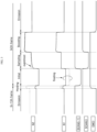
- Figure 3 shows a waveform of a driving signal in Figure 2 and an associated potential at each node.
- an organic light-emitting display device 10 includes a display panel 10 including a plurality of pixel PXLs, a data driving circuit 12 for driving data-lines 14 of the display panel 10, a gate driving circuit 13 for driving scan-lines 15 of the display panel 10, and a timing controller 11 for controlling the driving timing of the data driving circuit 12 and the gate driving circuit 13
- the display panel 10 includes scan-lines 15 and data-lines 14 that intersect with each other.
- a plurality of pixel regions corresponding to the plurality of pixel PXLs respectively are defined as the intersection regions between the scan-lines 15 and the data-lines 14, respectively.
- the plurality of pixel regions are arranged in a matrix form in the display region.
- the display panel 10 further includes, per each horizontal line of the plurality of pixel PXLs, an emission-line for supplying an emission signal EM, a first driving power supply line for supplying a first driving voltage VDD, a second driving power supply line for supplying a second driving voltage VSS having a potential lower than the first driving voltage VDD, a reference power supply line for supplying a reference voltage VREF via an initialization power supply.
- the reference voltage VREF is set to a potential lower than a trigger voltage of the organic light-emitting element.
- the display panel 10 may include first and second reference power supply lines connected to first and second initialization power supplies, respectively, for supplying first and second reference voltages having different voltage levels.
- the timing controller 11 rearranges digital video data RGB input from the outside based on a resolution of the display panel 10.
- the controller 11 supplies the rearranged digital video data RGB' to the data driving circuit 12.
- the timing controller 11 generates and output a data control signal DDC for controlling operation timing of the data driving circuit 12, and a gate control signal GDC for controlling operation timing of the gate driving circuit 13, based on timing signals such as a vertical synchronization signal Vsync, a horizontal synchronization signal Hsync, a dot clock signal DCLK, and a data enable signal DE, etc.
- the data driving circuit 12 converts the rearranged digital video data RGB' into an analog data voltage based on the data control signal DDC. Further, the data driving circuit 12 supplies a data signal (VDATA in FIG. 2 ) to the pixels in each horizontal line for each horizontal period based on the rearranged digital video data RGB'.
- VDATA data signal
- the gate driving circuit 13 may generate a scan signal SCAN and an emission signal EM based on the gate control signal GDC.
- the gate driving circuit 13 may include a scan drive unit and an emission drive unit.
- the scan drive unit may sequentially supply a scan signal SCAN to the scan lines in each horizontal line.
- the emission drive unit may supply the emission signal EM to the emission lines in each horizontal line for each horizontal period.
- the gate driving circuit 13 may be disposed in a non-display region in the display panel 10 in a GIP (Gate-Driver In Panel) mode.
- GIP Gate-Driver In Panel
- each of the plurality of pixel PXLs includes an organic light-emitting element OLED, a driving transistor DT, first to sixth transistors T1, T2 , T3, T4, T5, and T6, and a capacitor Cst.
- the driving transistor DT, the first transistor T1, and the capacitor Cst together define a pixel driving circuit for supplying driving current to the organic light-emitting element OLED for each frame, while the remaining second to sixth transistors T2 to T6 together define a compensation circuit for compensating the threshold voltage of the driving transistor DT.
- the pixel illustrated in Figure 2 may be one of pixels arranged in the i-th horizontal line among a plurality of pixels.
- i is greater than 2
- N is the total number of horizontal lines.
- the organic light-emitting element OLED may include an anode and a cathode, and an organic light-emitting layer disposed therebetween.
- the organic light-emitting layer includes a hole injection layer, a hole transport layer, a light emitting layer, and an electron transport layer.
- the organic light-emitting layer may further include an electron injection layer.
- the driving transistor DT is connected in series with the organic light-emitting element OLED and is disposed between the first driving power supply line for supplying the first driving voltage VDD and the second driving power supply line for supplying the second driving voltage VSS having a potential lower than the first driving power supply.
- a gate electrode thereof is connected to the capacitor Cst.
- One of first and second electrodes (source electrode and drain electrode) thereof is connected to the first driving power supply VDD, while the other thereof is connected to a third node N3.
- this driving transistor DT turns on based on a turn-on signal supplied from the capacitor Cst, the organic light-emitting element OLED is supplied with the driving current.
- first transistor T1 a gate electrode thereof is connected to an i-th scan-line for supplying the i-th scan signal SCAN(i).
- One of first and second electrodes (source electrode and drain electrode) thereof, for example, the source electrode, is connected to a data-line for supplying the data voltage VDATA, while the other thereof, for example, the drain electrode, is connected to the first node N1.
- the first node N1 is a joint point between the first transistor T1 and the capacitor Cst.
- the capacitor Cst is connected between the first node N1 and a second node N2.
- the second node N2 is a joint point between the capacitor Cst and the driving transistor DT.
- a first electrode of the capacitor Cst is connected to the first node N1 receiving the data voltage VDATA via the first transistor T1, while a second electrode of the capacitor Cst is connected to the second node N2 corresponding to the gate electrode of the driving transistor DT.
- This capacitor Cst supplies the turn-on signal to the gate electrode of the driving transistor DT at least based on the data voltage VDATA.
- the second transistor T2 turns on based on an (i-1)-th scan signal SCAN(i-1)
- a reference voltage VREF is supplied to the second node N2.
- the (i-1)-th scan signal SCAN(i-1) is a signal supplied via a (i-1)-th scan-line corresponding to a previous horizontal line.
- a gate electrode of the second transistor T2 is connected to the (i-1)-th scan-line for supplying the (i-1)-th scan signal SCAN(i-1).
- a gate electrode of the third transistor T3 is connected to the i-th emission-line for supplying the emission signal EM(i).
- One of first and second electrodes (source and drain electrodes) of the transistor T3, for example, the source electrode, is connected to the reference power supply line for supplying the reference voltage VREF, while the other thereof, for example, the drain electrode, is connected to the first node N1.
- a fourth transistor T4 is connected between the second node N2 and the third node N3, and turns on based on the i-th scan signal SCAN(i).
- the second node N2 corresponds to the gate electrode of the driving transistor DT.
- the third node N3 corresponds to the second electrode of the driving transistor DT, for example, the drain electrode, which is not connected to the first driving power supply VDD. That is, the fourth transistor T4 is disposed between the gate electrode and the drain electrode of the driving transistor DT.
- a gate electrode of the fourth transistor T4 is connected to the i-th scan-line for supplying the i-th scan signal SCAN(i).
- One of first and second electrodes (source and drain electrodes) of the transistor T4, for example, the source electrode, is connected to the third 3 node N3, while the other thereof, for example, the drain electrode is coupled to the 2 node N2.
- the gate electrode and the drain electrode of the driving transistor DT are connected to each other.
- a potential of the gate electrode of the driving transistor DT becomes close to a threshold voltage.
- a difference voltage VDD-Vth between the first driving voltage VDD of the first driving power supply line and the threshold voltage of the driving transistor DT is supplied to the third node N3 via the driving transistor DT.
- the difference voltage VDD-Vth of the third node N3 is supplied to the second node N2 via the turned-on fourth transistor T4.
- the fifth transistor T5 is connected between the third node N3 and the anode of the organic light-emitting element OLED.
- the fifth transistor T5 turns on based on the emission signal EM(i).
- a gate electrode of the fifth transistor T5 is connected to the i-th emission-line for supplying the emission signal EM(i).
- the cathode of the organic light-emitting element OLED is connected to the second driving power supply line which supplies the second driving voltage VSS.
- the reference voltage VREF is supplied to a fourth node N4.
- the fourth node N4 is a joint point between the fifth transistor T5 and the organic light-emitting element OLED.
- a gate electrode of the sixth transistor T6 is connected to the i-th scan-line for supplying the i-th scan signal SCAN(i).
- One of first and second electrodes (source electrode and drain electrode) of the sixth transistor T6, for example, the source electrode is connected to the reference power supply line, while the other thereof, for example, the drain electrode, is connected to the fourth node N4.
- the (i-1)-th scan signal SCAN (i-1), the i-th scan signal SCAN(i), and the emission signal EM(i) is supplied to the corresponding pixel PXL from the gate driving circuit (13 of FIG. 1 ).
- the (i-1)-th scan signal SCAN(i-1) is supplied at a turn-on level (low level in FIG. 3 ), while each of the i-th scan signal SCAN(i) and the emission signal EM(i) is supplied at a turn-off level (high level in Figure 3 ).
- the second transistor T2 is turned on based on the (i-1)-th scan signal SCAN(i-1) at the turn-on level.
- a potential of the second node N2 is initialized to the reference voltage VREF.
- the i-th scan signal SCAN(i) is supplied at a turn-on level (low level in FIG. 3 ), while each of the (i-1)-th scan signal SCAN(i-1) and emission signal EM(i) is supplied at a turn-off level (high level in FIG. 3 ).
- the second transistor T2 is turned off based on the (i-1)-th scan signal SCAN(i-1) at the turn-off level.
- the first transistor T1, the fourth transistor T4 and the sixth transistor T6 are turned on based on the i-th scan signal SCAN(i) at the turn-on level.
- the data voltage VDATA is supplied to the first node N1 via the turned-on first transistor T1. That is, the data voltage VDATA is supplied to one end of the capacitor Cst.
- a potential of the gate electrode of the driving transistor DT is gradually changed to be close to the threshold voltage of the driving transistor DT via the turned-on fourth transistor T4.
- the difference voltage VDD-Vth between the first driving voltage VDD and the threshold voltage Vth of the driving transistor DT is supplied to the second node N2 via the driving transistor DT and the fourth transistor T4.
- the reference voltage VREF is supplied to the fourth node N4 via the sixth transistor T6 which has been turned-on. This prevents the driving of the organic light-emitting element OLED for the sampling period (Sampling).
- Boosting For a boosting period (Boosting), all of the (i-1)-th scan signal SCAN(i-1), the i-th scan signal SCAN(i) and the i-th emission signal EM(i) are supplied at a turn-off level.
- all of the first to sixth transistors T1, T2, T3, T4, T5, and T6, including the first, fourth, and sixth transistors T1, T4, and T6 are turned off.
- the potential of the second node N2 is boosted by parasitic capacitances of the capacitor Cst and of the fourth transistor T4.
- the emission signal EM(i) is supplied at turn-on level, while each of the (i-1)-th scan signal SCAN(i-1) and the i-th scan signal SCAN(i) is supplied at a turn-off level.
- the third transistor T3 and the fifth transistor T5 are turned on based on the emission signal EM (i) at the turn-on level.
- the reference voltage VREF is supplied to the first node N1 via the third transistor T3 which has been turned on.
- the driving current of the driving transistor DT corresponding to the voltage of the second node is supplied to the organic light-emitting element OLED via the fifth transistor T5 which has been turned-on.
- the present configuration may turn the second transistor T2, and, thus, initialize the second node N2, that is, the second electrode of the capacitor Cst, and the gate electrode of the driving transistor DT to the reference voltage VREF.
- the second transistor T2 is turned on based on the (i-1)-th scan signal SCAN(i-1), unlike the first, fourth and sixth transistors T1, T4 and T6. That is, when the second transistor T2 is turned on, the first, fourth, and sixth transistors T1, T4, and T6 are not turned on.
- a current path including the driving transistor DT, the fourth and sixth transistors T4 and T6 may be suppressed.
- the first driving power supply for supplying the first driving voltage VDD and the initialization power supply for supplying the reference voltage VREF are prevented from being connected to each other.
- the ripple in the initialization power supply may be suppressed.
- the second transistor T2 may be turned on in a response to the (i-1)-th scan signal SCAN(i-1), i.e., a signal supplied through a scan line corresponding to a previous horizontal line.
- the gate driving circuit (13 in Fig. 1 ) may be implemented as a scan drive unit and an emission drive unit corresponding to each horizontal line, the gate driving circuit 13 may be designed simply and easily. As a result, a width of a bezel region in the organic light-emitting display device may be reduced due to the GIP-based gate driving circuit 13.
- the potential of the second node N2 is initialized to the reference voltage VREF, while the potential of the first node N1 is in a floating state (floating).
- the potential of the second node N2 may have an overshoot waveform at an initial point of the sampling period, especially when a black luminance is expressed in the previous frame ((k-1)-th frame).
- a luminance difference occurs between horizontal lines depending on the luminance in the previous frame ((k-1)-th frame).
- a second example is provided in which both potentials of the first and second nodes N1 and N2 are initialized for the initialization period (Initial).
- Figure 4 shows an equivalent circuit corresponding to any one pixel in an organic light-emitting display device according to the second example of the present disclosure.
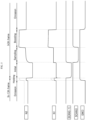
- Figure 5 shows a waveform of a driving signal in Figure 4 and an associated potential at each node.
- the organic light-emitting display device further includes a seventh transistor T7.
- the seventh transistor T7 When the seventh transistor T7 is turned on based on the (i-1)-th scan signal SCAN(i-1), the reference voltage VREF is supplied to the first node N1 via the turned-on seventh transistor T7. Except for the presence of the seventh transistor T7, a configuration of the second example is the same as that of the first example illustrated in Figures 1 to 3 . Therefore, the descriptions of the overlapping portions between the first and second examples may be omitted.
- the seventh transistor T7 is connected between the first node N1 and the reference power supply line for supplying the reference voltage VREF.
- a gate electrode of the seventh transistor T7 is connected to the (i-1)-th scan line for supplying the (i-1)-th scan signal SCAN(i-1).
- One of first and second electrodes (source electrode and drain electrode) of the seventh transistor T7, for example, the source electrode is connected to the reference power supply line for supplying the reference voltage VREF, while the other thereof, for example, the drain electrode, is connected to the first node N1.
- each of the second transistor T2 and the seventh transistor T7 is turned on based on the (i-1)-th scan signal SCAN (i-1) at the turn-on level.
- the potential of the second node N2 is initialized to the reference voltage VREF via the turned-on second transistor T2, while the potential of the first node N1 is initialized to the reference voltage VREF via the turned-on seventh transistor T7.
- the potential of the second node N2 may be prevented from fluctuating depending on the luminance of the previous frame ((k-1)-th frame). Therefore, the luminance difference between horizontal lines depending on the luminance in the previous frame ((k-1)-th frame) may be suppressed.
- a reference voltage for initializing the first node N1 and a reference voltage for initializing the second node N2 may have different voltage levels.
- Figure 6 shows an equivalent circuit corresponding to any one pixel in an organic light-emitting display device according to a third example of the present disclosure.
- a first reference voltage VREF1 is supplied to the second node N2 via the turned-on transistor t2.
- the seventh transistor T7 turns on, the first node N1 is supplied with a second reference voltage VREF2 which is different from the first reference voltage VREF1.
- a configuration of the third example is the same as those of the first and second examples illustrated in Figures 1 to 5 , except that, in the third example, the first reference voltage for initializing the first node N1 and the second reference voltage for initializing the second node N2 have different voltage levels. Therefore, the descriptions of the overlapping portions between the first, second, and third examples may be omitted.
- the first reference voltage VREF1 is supplied to the second node N2 via the turned-on second transistor.
- first and second electrodes (source and drain electrodes) of the second transistor T2 for example, the source electrode
- a first reference power supply line for supplying the first reference voltage VREF 1
- the other thereof, for example, the drain electrode is connected to the second node N2.
- the seventh transistor T7 turns on based on the (i-1)-th scan signal SCAN(i-1)
- the second reference voltage VREF2 is supplied to the first node N1 via the turned-on seventh transistor.
- one of first and second electrodes (source and drain electrodes) of the seventh transistor T7 is connected to a second reference power supply line for supplying the second reference voltage VREF2, while the other thereof, for example, the drain electrode, is connected to the first node N1.
- the capacitor Cst may be initialized to a difference voltage between the first reference voltage VREF1 and the second reference voltage VREF2.
- a response speed in the sampling period may be easily adjusted via the first reference voltage VREF1 and the second reference voltage VREF2.
- the third example may allow easy compensation for degradation in overall pixels over the driving time of the organic light-emitting display device.
- the first reference voltage (VREF1 in Figure 6 ) according to the third example may be set to a range as similar to a range of an operation-trigger voltage of the organic light-emitting element OLED.
- the first reference voltage (VREF1 in FIG. 6 ) according to the third example may be greater than or equal to the operation-trigger voltage of the organic light-emitting element OLED.
- Figure 7 shows an equivalent circuit corresponding to any one pixel in an organic light-emitting display device according to a fourth example of the present disclosure.
- one of first and second electrodes (source and drain electrodes) of the second transistor T2 is connected to the second driving power supply line for supplying the second driving voltage VSS, while, the other thereof, for example, the drain electrode, is connected to the second node N2.
- the seventh transistor T7 turns on based on the (i-1)-th scan signal SCAN(i-1), the reference voltage VREF is supplied to the first node N1 via the turned-on seventh transistor.
- the sixth transistor T6 When the sixth transistor T6 is turned on based on the i-th scan signal SCAN(i), the second driving voltage VSS is supplied to the fourth node N4 via the turned-on sixth transistor.
- one of first and second electrodes (source and drain electrodes) of the sixth transistor T6, for example, the source electrode, is connected to the second driving power supply line for supplying the second driving voltage VSS, while the other thereof, for example, the drain electrode, is connected to the fourth node N4.
- the second driving voltage VSS is supplied to the fourth node N4, that is, the anode of the organic light-emitting element OLED. Therefore, the organic light-emitting element OLED may be prevented from malfunctioning due to the off-current of the sixth transistor T6. Thus, an image quality of the device may be improved.
Landscapes
- Engineering & Computer Science (AREA)
- Physics & Mathematics (AREA)
- Computer Hardware Design (AREA)
- General Physics & Mathematics (AREA)
- Theoretical Computer Science (AREA)
- Microelectronics & Electronic Packaging (AREA)
- Electroluminescent Light Sources (AREA)
- Control Of Indicators Other Than Cathode Ray Tubes (AREA)
- Control Of El Displays (AREA)
- Devices For Indicating Variable Information By Combining Individual Elements (AREA)
Applications Claiming Priority (1)
| Application Number | Priority Date | Filing Date | Title |
|---|---|---|---|
| KR1020170126235A KR102623352B1 (ko) | 2017-09-28 | 2017-09-28 | 유기발광표시장치 및 그의 구동방법 |
Publications (2)
| Publication Number | Publication Date |
|---|---|
| EP3462437A1 EP3462437A1 (en) | 2019-04-03 |
| EP3462437B1 true EP3462437B1 (en) | 2023-05-24 |
Family
ID=63678532
Family Applications (1)
| Application Number | Title | Priority Date | Filing Date |
|---|---|---|---|
| EP18196056.8A Active EP3462437B1 (en) | 2017-09-28 | 2018-09-21 | Organic light emitting display device and method for driving the same |
Country Status (6)
| Country | Link |
|---|---|
| US (1) | US10733940B2 (zh) |
| EP (1) | EP3462437B1 (zh) |
| JP (1) | JP6710251B2 (zh) |
| KR (1) | KR102623352B1 (zh) |
| CN (1) | CN109584791B (zh) |
| TW (1) | TWI682380B (zh) |
Families Citing this family (17)
| Publication number | Priority date | Publication date | Assignee | Title |
|---|---|---|---|---|
| KR102623352B1 (ko) * | 2017-09-28 | 2024-01-09 | 엘지디스플레이 주식회사 | 유기발광표시장치 및 그의 구동방법 |
| CN109727570A (zh) * | 2017-10-31 | 2019-05-07 | 云谷(固安)科技有限公司 | 一种像素电路及其驱动方法、显示装置 |
| CN107991817A (zh) * | 2017-11-29 | 2018-05-04 | 武汉华星光电技术有限公司 | 一种显示面板及其制造方法和控制方法 |
| CN108806596A (zh) * | 2018-06-26 | 2018-11-13 | 京东方科技集团股份有限公司 | 像素驱动电路及方法、显示装置 |
| TWI703546B (zh) * | 2019-05-30 | 2020-09-01 | 友達光電股份有限公司 | 發光二極體畫素電路及其驅動方法 |
| CN112424856B (zh) * | 2019-06-03 | 2023-03-14 | 京东方科技集团股份有限公司 | 像素电路、像素电路的驱动方法、显示装置及其驱动方法 |
| KR102633822B1 (ko) * | 2019-09-06 | 2024-02-06 | 엘지디스플레이 주식회사 | 발광표시장치 및 이의 구동방법 |
| KR20210086441A (ko) * | 2019-12-30 | 2021-07-08 | 엘지디스플레이 주식회사 | 표시패널과 그 리페어 방법 |
| CN111354308A (zh) * | 2020-04-09 | 2020-06-30 | 上海天马有机发光显示技术有限公司 | 一种像素驱动电路、有机发光显示面板及显示装置 |
| CN111627387B (zh) * | 2020-06-24 | 2022-09-02 | 京东方科技集团股份有限公司 | 像素驱动电路及其驱动方法、显示面板及显示装置 |
| US11922877B2 (en) * | 2020-07-22 | 2024-03-05 | Sharp Kabushiki Kaisha | Display device enabling both high-frequency drive and low-frequency drive |
| CN114450741A (zh) * | 2020-08-19 | 2022-05-06 | Oled沃克斯有限责任公司 | 串扰减少的像素电路 |
| KR20220155537A (ko) | 2021-05-14 | 2022-11-23 | 삼성디스플레이 주식회사 | 화소 및 이를 포함하는 표시 장치 |
| KR20230006730A (ko) * | 2021-07-02 | 2023-01-11 | 삼성디스플레이 주식회사 | 표시장치 |
| CN115602116A (zh) | 2021-07-08 | 2023-01-13 | 乐金显示有限公司(Kr) | 像素电路和包括像素电路的显示装置 |
| KR20230046700A (ko) * | 2021-09-30 | 2023-04-06 | 엘지디스플레이 주식회사 | 픽셀 회로와 이를 포함한 표시장치 |
| CN114093321B (zh) * | 2021-11-30 | 2023-11-28 | 厦门天马微电子有限公司 | 像素驱动电路、驱动方法、显示面板及显示装置 |
Citations (1)
| Publication number | Priority date | Publication date | Assignee | Title |
|---|---|---|---|---|
| EP3147894A1 (en) * | 2015-09-25 | 2017-03-29 | LG Display Co., Ltd. | Organic light-emitting diode (oled) display panel, oled display device and method for driving the same |
Family Cites Families (23)
| Publication number | Priority date | Publication date | Assignee | Title |
|---|---|---|---|---|
| JP2011191449A (ja) * | 2010-03-12 | 2011-09-29 | Hitachi Displays Ltd | 画像表示装置 |
| KR101162864B1 (ko) * | 2010-07-19 | 2012-07-04 | 삼성모바일디스플레이주식회사 | 화소 및 이를 이용한 유기 전계발광 표시장치 |
| KR101859474B1 (ko) * | 2011-09-05 | 2018-05-23 | 엘지디스플레이 주식회사 | 유기 발광 다이오드 표시 장치의 화소 회로 |
| CN103700342B (zh) | 2013-12-12 | 2017-03-01 | 京东方科技集团股份有限公司 | Oled像素电路及驱动方法、显示装置 |
| CN104021754B (zh) | 2014-05-22 | 2016-01-06 | 京东方科技集团股份有限公司 | 一种像素电路、有机电致发光显示面板及显示装置 |
| CN203882588U (zh) * | 2014-06-13 | 2014-10-15 | 京东方科技集团股份有限公司 | 像素驱动电路、阵列基板及显示装置 |
| CN105225636B (zh) * | 2014-06-13 | 2017-05-31 | 京东方科技集团股份有限公司 | 像素驱动电路、驱动方法、阵列基板及显示装置 |
| CN104091563B (zh) | 2014-06-27 | 2016-03-09 | 京东方科技集团股份有限公司 | 像素电路及其驱动方法、有机发光显示面板及显示装置 |
| KR102218779B1 (ko) | 2014-07-04 | 2021-02-19 | 엘지디스플레이 주식회사 | Oled 표시 장치 |
| KR102265368B1 (ko) * | 2015-01-13 | 2021-06-15 | 삼성디스플레이 주식회사 | 화소, 이를 포함하는 표시 장치 및 그 구동방법 |
| CN104992674A (zh) * | 2015-07-24 | 2015-10-21 | 上海和辉光电有限公司 | 一种像素补偿电路 |
| CN205004016U (zh) * | 2015-08-04 | 2016-01-27 | 信利(惠州)智能显示有限公司 | 一种有机发光二极管的驱动电路 |
| KR102622957B1 (ko) * | 2015-12-29 | 2024-01-10 | 삼성디스플레이 주식회사 | 휘도 컨트롤러 및 이를 포함하는 유기 발광 표시 장치 |
| US10262586B2 (en) | 2016-03-14 | 2019-04-16 | Apple Inc. | Light-emitting diode display with threshold voltage compensation |
| CN106057126B (zh) * | 2016-05-26 | 2019-04-16 | 上海天马有机发光显示技术有限公司 | 一种像素电路及其驱动方法 |
| US10482820B2 (en) * | 2016-06-21 | 2019-11-19 | Novatek Microelectronics Corp. | Method of compensating luminance of OLED and display system using the same |
| CN205920745U (zh) * | 2016-08-22 | 2017-02-01 | 京东方科技集团股份有限公司 | 像素电路、显示面板及显示设备 |
| CN106097964B (zh) * | 2016-08-22 | 2018-09-18 | 京东方科技集团股份有限公司 | 像素电路、显示面板、显示设备及驱动方法 |
| CN106486064A (zh) * | 2016-12-28 | 2017-03-08 | 武汉华星光电技术有限公司 | Oled驱动电路及oled显示器 |
| CN106875893B (zh) * | 2017-03-07 | 2019-03-15 | 京东方科技集团股份有限公司 | 像素电路和具有该像素电路的显示装置 |
| CN106952617B (zh) * | 2017-05-18 | 2019-01-25 | 京东方科技集团股份有限公司 | 像素驱动电路及方法、显示装置 |
| CN107274829B (zh) * | 2017-07-10 | 2020-04-14 | 上海天马有机发光显示技术有限公司 | 一种有机电致发光显示面板及显示设备 |
| KR102623352B1 (ko) * | 2017-09-28 | 2024-01-09 | 엘지디스플레이 주식회사 | 유기발광표시장치 및 그의 구동방법 |
-
2017
- 2017-09-28 KR KR1020170126235A patent/KR102623352B1/ko active IP Right Grant
-
2018
- 2018-09-21 EP EP18196056.8A patent/EP3462437B1/en active Active
- 2018-09-27 US US16/144,682 patent/US10733940B2/en active Active
- 2018-09-28 CN CN201811139714.5A patent/CN109584791B/zh active Active
- 2018-09-28 TW TW107134330A patent/TWI682380B/zh active
- 2018-09-28 JP JP2018183994A patent/JP6710251B2/ja active Active
Patent Citations (1)
| Publication number | Priority date | Publication date | Assignee | Title |
|---|---|---|---|---|
| EP3147894A1 (en) * | 2015-09-25 | 2017-03-29 | LG Display Co., Ltd. | Organic light-emitting diode (oled) display panel, oled display device and method for driving the same |
Also Published As
| Publication number | Publication date |
|---|---|
| CN109584791B (zh) | 2022-04-08 |
| US10733940B2 (en) | 2020-08-04 |
| TW201915992A (zh) | 2019-04-16 |
| JP2019066847A (ja) | 2019-04-25 |
| JP6710251B2 (ja) | 2020-06-17 |
| KR102623352B1 (ko) | 2024-01-09 |
| KR20190036841A (ko) | 2019-04-05 |
| TWI682380B (zh) | 2020-01-11 |
| EP3462437A1 (en) | 2019-04-03 |
| US20190096336A1 (en) | 2019-03-28 |
| CN109584791A (zh) | 2019-04-05 |
Similar Documents
| Publication | Publication Date | Title |
|---|---|---|
| EP3462437B1 (en) | Organic light emitting display device and method for driving the same | |
| JP6773632B2 (ja) | 表示パネルおよび電界発光表示装置 | |
| EP3151233B1 (en) | Organic light emitting diode display | |
| KR102570832B1 (ko) | Oled 표시 장치 및 그의 구동 방법 | |
| US9105213B2 (en) | Organic light emitting diode display and method of driving the same | |
| US9111488B2 (en) | Organic light emitting diode display device and method of driving the same | |
| US10269294B2 (en) | Organic light emitting diode display device and method for driving the same | |
| KR101760090B1 (ko) | 화소 및 이를 이용한 유기전계발광 표시장치 | |
| US9330603B2 (en) | Organic light emitting diode display device and method of driving the same | |
| US9491829B2 (en) | Organic light emitting diode display and method of driving the same | |
| US9324275B2 (en) | Organic light emitting diode display device and method for driving the same | |
| US8723843B2 (en) | Pixel driving circuit with capacitor having threshold voltages information storing function, pixel driving method and light emitting display device | |
| KR102345423B1 (ko) | 유기발광표시장치 및 그의 구동방법 | |
| KR20170074618A (ko) | 유기 발광 표시 장치의 서브-화소 및 이를 포함하는 유기 발광 표시 장치 | |
| US10902795B2 (en) | Pixel for organic light emitting diode display and OLED display | |
| US8432336B2 (en) | Pixel and organic light emitting display device using the same | |
| KR20120069481A (ko) | 발광 표시 장치 및 그의 구동 방법 | |
| KR101048951B1 (ko) | 유기전계발광 표시장치 | |
| KR20190010059A (ko) | 유기발광 표시장치 | |
| KR102696836B1 (ko) | 발광 제어 신호 발생부 및 이를 포함하는 발광 표시 장치 | |
| KR102473218B1 (ko) | 유기 발광 표시장치 | |
| KR20100072657A (ko) | 유기전계발광소자 및 그 구동방법 | |
| KR20190070585A (ko) | 유기발광표시장치 및 그의 구동방법 |
Legal Events
| Date | Code | Title | Description |
|---|---|---|---|
| PUAI | Public reference made under article 153(3) epc to a published international application that has entered the european phase |
Free format text: ORIGINAL CODE: 0009012 |
|
| STAA | Information on the status of an ep patent application or granted ep patent |
Free format text: STATUS: REQUEST FOR EXAMINATION WAS MADE |
|
| 17P | Request for examination filed |
Effective date: 20180921 |
|
| AK | Designated contracting states |
Kind code of ref document: A1 Designated state(s): AL AT BE BG CH CY CZ DE DK EE ES FI FR GB GR HR HU IE IS IT LI LT LU LV MC MK MT NL NO PL PT RO RS SE SI SK SM TR |
|
| AX | Request for extension of the european patent |
Extension state: BA ME |
|
| RBV | Designated contracting states (corrected) |
Designated state(s): AL AT BE BG CH CY CZ DE DK EE ES FI FR GB GR HR HU IE IS IT LI LT LU LV MC MK MT NL NO PL PT RO RS SE SI SK SM TR |
|
| STAA | Information on the status of an ep patent application or granted ep patent |
Free format text: STATUS: EXAMINATION IS IN PROGRESS |
|
| 17Q | First examination report despatched |
Effective date: 20190814 |
|
| STAA | Information on the status of an ep patent application or granted ep patent |
Free format text: STATUS: EXAMINATION IS IN PROGRESS |
|
| STAA | Information on the status of an ep patent application or granted ep patent |
Free format text: STATUS: EXAMINATION IS IN PROGRESS |
|
| GRAP | Despatch of communication of intention to grant a patent |
Free format text: ORIGINAL CODE: EPIDOSNIGR1 |
|
| STAA | Information on the status of an ep patent application or granted ep patent |
Free format text: STATUS: GRANT OF PATENT IS INTENDED |
|
| INTG | Intention to grant announced |
Effective date: 20230120 |
|
| GRAS | Grant fee paid |
Free format text: ORIGINAL CODE: EPIDOSNIGR3 |
|
| GRAA | (expected) grant |
Free format text: ORIGINAL CODE: 0009210 |
|
| STAA | Information on the status of an ep patent application or granted ep patent |
Free format text: STATUS: THE PATENT HAS BEEN GRANTED |
|
| AK | Designated contracting states |
Kind code of ref document: B1 Designated state(s): AL AT BE BG CH CY CZ DE DK EE ES FI FR GB GR HR HU IE IS IT LI LT LU LV MC MK MT NL NO PL PT RO RS SE SI SK SM TR |
|
| REG | Reference to a national code |
Ref country code: GB Ref legal event code: FG4D |
|
| REG | Reference to a national code |
Ref country code: CH Ref legal event code: EP |
|
| REG | Reference to a national code |
Ref country code: DE Ref legal event code: R096 Ref document number: 602018050119 Country of ref document: DE |
|
| REG | Reference to a national code |
Ref country code: AT Ref legal event code: REF Ref document number: 1570038 Country of ref document: AT Kind code of ref document: T Effective date: 20230615 |
|
| REG | Reference to a national code |
Ref country code: IE Ref legal event code: FG4D |
|
| REG | Reference to a national code |
Ref country code: LT Ref legal event code: MG9D |
|
| REG | Reference to a national code |
Ref country code: NL Ref legal event code: MP Effective date: 20230524 |
|
| REG | Reference to a national code |
Ref country code: AT Ref legal event code: MK05 Ref document number: 1570038 Country of ref document: AT Kind code of ref document: T Effective date: 20230524 |
|
| PG25 | Lapsed in a contracting state [announced via postgrant information from national office to epo] |
Ref country code: SE Free format text: LAPSE BECAUSE OF FAILURE TO SUBMIT A TRANSLATION OF THE DESCRIPTION OR TO PAY THE FEE WITHIN THE PRESCRIBED TIME-LIMIT Effective date: 20230524 Ref country code: PT Free format text: LAPSE BECAUSE OF FAILURE TO SUBMIT A TRANSLATION OF THE DESCRIPTION OR TO PAY THE FEE WITHIN THE PRESCRIBED TIME-LIMIT Effective date: 20230925 Ref country code: NO Free format text: LAPSE BECAUSE OF FAILURE TO SUBMIT A TRANSLATION OF THE DESCRIPTION OR TO PAY THE FEE WITHIN THE PRESCRIBED TIME-LIMIT Effective date: 20230824 Ref country code: NL Free format text: LAPSE BECAUSE OF FAILURE TO SUBMIT A TRANSLATION OF THE DESCRIPTION OR TO PAY THE FEE WITHIN THE PRESCRIBED TIME-LIMIT Effective date: 20230524 Ref country code: ES Free format text: LAPSE BECAUSE OF FAILURE TO SUBMIT A TRANSLATION OF THE DESCRIPTION OR TO PAY THE FEE WITHIN THE PRESCRIBED TIME-LIMIT Effective date: 20230524 Ref country code: AT Free format text: LAPSE BECAUSE OF FAILURE TO SUBMIT A TRANSLATION OF THE DESCRIPTION OR TO PAY THE FEE WITHIN THE PRESCRIBED TIME-LIMIT Effective date: 20230524 |
|
| PGFP | Annual fee paid to national office [announced via postgrant information from national office to epo] |
Ref country code: GB Payment date: 20230821 Year of fee payment: 6 |
|
| PG25 | Lapsed in a contracting state [announced via postgrant information from national office to epo] |
Ref country code: RS Free format text: LAPSE BECAUSE OF FAILURE TO SUBMIT A TRANSLATION OF THE DESCRIPTION OR TO PAY THE FEE WITHIN THE PRESCRIBED TIME-LIMIT Effective date: 20230524 Ref country code: PL Free format text: LAPSE BECAUSE OF FAILURE TO SUBMIT A TRANSLATION OF THE DESCRIPTION OR TO PAY THE FEE WITHIN THE PRESCRIBED TIME-LIMIT Effective date: 20230524 Ref country code: LV Free format text: LAPSE BECAUSE OF FAILURE TO SUBMIT A TRANSLATION OF THE DESCRIPTION OR TO PAY THE FEE WITHIN THE PRESCRIBED TIME-LIMIT Effective date: 20230524 Ref country code: LT Free format text: LAPSE BECAUSE OF FAILURE TO SUBMIT A TRANSLATION OF THE DESCRIPTION OR TO PAY THE FEE WITHIN THE PRESCRIBED TIME-LIMIT Effective date: 20230524 Ref country code: IS Free format text: LAPSE BECAUSE OF FAILURE TO SUBMIT A TRANSLATION OF THE DESCRIPTION OR TO PAY THE FEE WITHIN THE PRESCRIBED TIME-LIMIT Effective date: 20230924 Ref country code: HR Free format text: LAPSE BECAUSE OF FAILURE TO SUBMIT A TRANSLATION OF THE DESCRIPTION OR TO PAY THE FEE WITHIN THE PRESCRIBED TIME-LIMIT Effective date: 20230524 Ref country code: GR Free format text: LAPSE BECAUSE OF FAILURE TO SUBMIT A TRANSLATION OF THE DESCRIPTION OR TO PAY THE FEE WITHIN THE PRESCRIBED TIME-LIMIT Effective date: 20230825 |
|
| PGFP | Annual fee paid to national office [announced via postgrant information from national office to epo] |
Ref country code: FR Payment date: 20230821 Year of fee payment: 6 Ref country code: DE Payment date: 20230822 Year of fee payment: 6 |
|
| PG25 | Lapsed in a contracting state [announced via postgrant information from national office to epo] |
Ref country code: FI Free format text: LAPSE BECAUSE OF FAILURE TO SUBMIT A TRANSLATION OF THE DESCRIPTION OR TO PAY THE FEE WITHIN THE PRESCRIBED TIME-LIMIT Effective date: 20230524 |
|
| PG25 | Lapsed in a contracting state [announced via postgrant information from national office to epo] |
Ref country code: SK Free format text: LAPSE BECAUSE OF FAILURE TO SUBMIT A TRANSLATION OF THE DESCRIPTION OR TO PAY THE FEE WITHIN THE PRESCRIBED TIME-LIMIT Effective date: 20230524 |
|
| PG25 | Lapsed in a contracting state [announced via postgrant information from national office to epo] |
Ref country code: SM Free format text: LAPSE BECAUSE OF FAILURE TO SUBMIT A TRANSLATION OF THE DESCRIPTION OR TO PAY THE FEE WITHIN THE PRESCRIBED TIME-LIMIT Effective date: 20230524 Ref country code: SK Free format text: LAPSE BECAUSE OF FAILURE TO SUBMIT A TRANSLATION OF THE DESCRIPTION OR TO PAY THE FEE WITHIN THE PRESCRIBED TIME-LIMIT Effective date: 20230524 Ref country code: RO Free format text: LAPSE BECAUSE OF FAILURE TO SUBMIT A TRANSLATION OF THE DESCRIPTION OR TO PAY THE FEE WITHIN THE PRESCRIBED TIME-LIMIT Effective date: 20230524 Ref country code: EE Free format text: LAPSE BECAUSE OF FAILURE TO SUBMIT A TRANSLATION OF THE DESCRIPTION OR TO PAY THE FEE WITHIN THE PRESCRIBED TIME-LIMIT Effective date: 20230524 Ref country code: DK Free format text: LAPSE BECAUSE OF FAILURE TO SUBMIT A TRANSLATION OF THE DESCRIPTION OR TO PAY THE FEE WITHIN THE PRESCRIBED TIME-LIMIT Effective date: 20230524 Ref country code: CZ Free format text: LAPSE BECAUSE OF FAILURE TO SUBMIT A TRANSLATION OF THE DESCRIPTION OR TO PAY THE FEE WITHIN THE PRESCRIBED TIME-LIMIT Effective date: 20230524 |
|
| REG | Reference to a national code |
Ref country code: DE Ref legal event code: R097 Ref document number: 602018050119 Country of ref document: DE |
|
| PLBE | No opposition filed within time limit |
Free format text: ORIGINAL CODE: 0009261 |
|
| STAA | Information on the status of an ep patent application or granted ep patent |
Free format text: STATUS: NO OPPOSITION FILED WITHIN TIME LIMIT |
|
| REG | Reference to a national code |
Ref country code: CH Ref legal event code: PL |
|
| 26N | No opposition filed |
Effective date: 20240227 |
|
| PG25 | Lapsed in a contracting state [announced via postgrant information from national office to epo] |
Ref country code: SI Free format text: LAPSE BECAUSE OF FAILURE TO SUBMIT A TRANSLATION OF THE DESCRIPTION OR TO PAY THE FEE WITHIN THE PRESCRIBED TIME-LIMIT Effective date: 20230524 |
|
| PG25 | Lapsed in a contracting state [announced via postgrant information from national office to epo] |
Ref country code: LU Free format text: LAPSE BECAUSE OF NON-PAYMENT OF DUE FEES Effective date: 20230921 |
|
| REG | Reference to a national code |
Ref country code: BE Ref legal event code: MM Effective date: 20230930 |
|
| PG25 | Lapsed in a contracting state [announced via postgrant information from national office to epo] |
Ref country code: SI Free format text: LAPSE BECAUSE OF FAILURE TO SUBMIT A TRANSLATION OF THE DESCRIPTION OR TO PAY THE FEE WITHIN THE PRESCRIBED TIME-LIMIT Effective date: 20230524 Ref country code: LU Free format text: LAPSE BECAUSE OF NON-PAYMENT OF DUE FEES Effective date: 20230921 Ref country code: IT Free format text: LAPSE BECAUSE OF FAILURE TO SUBMIT A TRANSLATION OF THE DESCRIPTION OR TO PAY THE FEE WITHIN THE PRESCRIBED TIME-LIMIT Effective date: 20230524 Ref country code: MC Free format text: LAPSE BECAUSE OF FAILURE TO SUBMIT A TRANSLATION OF THE DESCRIPTION OR TO PAY THE FEE WITHIN THE PRESCRIBED TIME-LIMIT Effective date: 20230524 |
|
| REG | Reference to a national code |
Ref country code: IE Ref legal event code: MM4A |
|
| PG25 | Lapsed in a contracting state [announced via postgrant information from national office to epo] |
Ref country code: IE Free format text: LAPSE BECAUSE OF NON-PAYMENT OF DUE FEES Effective date: 20230921 |
|
| PG25 | Lapsed in a contracting state [announced via postgrant information from national office to epo] |
Ref country code: CH Free format text: LAPSE BECAUSE OF NON-PAYMENT OF DUE FEES Effective date: 20230930 |
|
| PG25 | Lapsed in a contracting state [announced via postgrant information from national office to epo] |
Ref country code: IE Free format text: LAPSE BECAUSE OF NON-PAYMENT OF DUE FEES Effective date: 20230921 Ref country code: CH Free format text: LAPSE BECAUSE OF NON-PAYMENT OF DUE FEES Effective date: 20230930 |
|
| PG25 | Lapsed in a contracting state [announced via postgrant information from national office to epo] |
Ref country code: BE Free format text: LAPSE BECAUSE OF NON-PAYMENT OF DUE FEES Effective date: 20230930 |