EP3451024A1 - Strahlungsdetektor und signalverarbeitungsvorrichtung zur strahlungsdetektion - Google Patents
Strahlungsdetektor und signalverarbeitungsvorrichtung zur strahlungsdetektion Download PDFInfo
- Publication number
- EP3451024A1 EP3451024A1 EP17789259.3A EP17789259A EP3451024A1 EP 3451024 A1 EP3451024 A1 EP 3451024A1 EP 17789259 A EP17789259 A EP 17789259A EP 3451024 A1 EP3451024 A1 EP 3451024A1
- Authority
- EP
- European Patent Office
- Prior art keywords
- signal
- pulse
- digital signal
- radiation
- denoising filter
- Prior art date
- Legal status (The legal status is an assumption and is not a legal conclusion. Google has not performed a legal analysis and makes no representation as to the accuracy of the status listed.)
- Granted
Links
Images


Classifications
-
- G—PHYSICS
- G01—MEASURING; TESTING
- G01T—MEASUREMENT OF NUCLEAR OR X-RADIATION
- G01T1/00—Measuring X-radiation, gamma radiation, corpuscular radiation, or cosmic radiation
- G01T1/16—Measuring radiation intensity
- G01T1/17—Circuit arrangements not adapted to a particular type of detector
Definitions
- the present invention relates to a radiation detection system and a signal processor used for the radiation detection system.
- a conventional radiation detection system is configured to convert the integrated amount of charge outputted from a radiation detection part having a semiconductor radiation detecting element such as an SDD (Silicon Drift Detector) into an integrated signal (e.g., a voltage signal) corresponding to the integrated amount by a conversion part such as a CSA (Charge Sensitive Amplifier), and input it to a pulse processor such as a DPP (Digital Pulse Processor).
- the pulse processor shapes the integrated signal to a pulse signal having, for example, a trapezoidal waveform.
- the peak value of the pulse signal corresponds to the energy of radiation.
- a radiation spectrum can be obtained by counting the pulse signal on a pulse height basis using a counter such as an MCA (Multi Channel Analyzer).
- the pulse processor in Patent Literature 1 is configured to mount therein multiple waveform shaping filters having different filter time constants PT.
- the pulse processor includes: a fast filter having a shorter filter time constant and mainly intended to detect radiation incidence; and a slow filter having a longer filter time constant and mainly intended to measure radiation energy.
- the slow filter is considered to have the shortest possible filter time constant PT so that pulse signals generated by incidence of different beams of radiation can be prevented from being excluded as a pile-up.
- Patent Literature 1 Japanese Unexamined Patent Publication JP-A2014-219362
- the filter time constant of the slow filter is made shorter than a certain value, the effect of white noise increases to fail to obtain sufficient S/N, and variations in measured energy values by the counter such as an MCA occur, thus deteriorating the energy resolution of an X-ray spectrum.
- the filter time constant PT in order to distinguish pulsed noise due to the white noise and a pulse signal caused by X-ray incidence to obtain sufficient S/N, it is conceivable to increase the filter time constant PT.
- a threshold value can be decreased by increasing the filter time constant PT to increase S/N, time resolution is deteriorated.
- S/N decreases to improve the time resolution, but the threshold value must be increased (trade-off).
- the present invention has been made in order to solve the above-described problems at once, and a main object thereof is to reduce white noise to improve radiation energy resolution, as well as to improve pulse detection time resolution.
- a radiation detection system includes: a radiation detector that outputs charge generated by incidence of radiation; a preamplifier that converts the generated charge into an analog signal; an A/D conversion part that converts the analog signal from the preamplifier into a digital signal; a waveform shaping part that generates a pulse signal from the digital signal from the A/D conversion part; a pulse height detection part that detects peak values of the pulse signal from the waveform shaping part; a count part that, on a pulse height basis, counts the peak values obtained by the pulse height detection part; and a denoising filter that is provided between the A/D conversion part and the pulse height detection part and removes noise from the digital signal or the pulse signal, in which the denoising filter is one that removes the noise by taking the weighted moving average of the values of the digital signal or the pulse signal with use of a weighting factor depending on the difference from a predetermined reference value.
- the waveform shaping part includes: a slow waveform output part that generates a pulse signal having long duration; and a fast waveform output part that generates a pulse signal having short duration.
- the denoising filter provided in the stage prior to the pulse height detection part takes the weighted moving average of the values of the digital signal or the pulse signal with use of the weighting factor depending on the difference from the predetermined reference value, the noise of the digital signal to be inputted to the waveform shaping part or the noise of the pulse signal to be inputted to the pulse height detection part can be removed. Specifically, the noise can be removed while smoothing step parts of the digital signal to be inputted to the slow waveform output part to suppress dulling, and radiation energy resolution can be improved.
- a filter time constant PT of the slow waveform output part can be more decreased, and also a pulse detection threshold value can be reduced to a lower energy side, so that together with an improvement in pulse detection time resolution and an improvement in pile-up detection performance, pulse detection can be performed in a lower energy region by the fast waveform output part.
- a radiation detection system includes: a radiation detector that outputs charge generated by incidence of radiation; a preamplifier that converts the generated charge into an analog signal; an A/D conversion part that converts the analog signal from the preamplifier into a digital signal; a denoising filter that removes noise from the digital signal from the A/D conversion part; and a gradient detection part that detects a step-based gradient from a digital signal having passed through the denoising filter, in which the denoising filter is one that removes the noise by taking the weighted moving average of the values of the digital signal with use of a weighting factor depending on the difference from a predetermined reference value.
- the denoising filter provided in the stage prior to the gradient detection part takes the weighted moving average of the values of the digital signal with use of the weighting factor depending on the difference from the predetermined reference value, thus making it easy to determine the rise of a step part due to the incidence of radiation in the gradient detection part, so that from the slope (gradient) of the rise, the incident position of the radiation in the radiation detector can be estimated, and a pile-up caused by the incidence of multiple beams of radiation can be detected.
- the reference value is one that changes for each interval in the weighted moving average.
- the denoising filter is configured to decrease the weighting factor as the difference from the reference value increases.
- to be configured to decrease the weighting factor as the difference from the reference value increases includes a monotonic decrease in the weighting factor depending on the difference from the reference value, or a stepwise decrease in the weighting factor depending on the difference from the reference value, i.e., includes one including a constant part in which the weighting factor does not change.
- the denoising filter desirably takes a weighted moving average in the time direction as well in terms of the accuracy of removing noise. That is, the denoising filter is desirably one that takes the weighted moving average of the values of the digital signal with use of a weighting factor depending on the time difference from a time point corresponding to the reference value. That is, the denoising filter takes the weighted moving average of the voltage values v(t) with use of a weighting factor w' depending on
- the denoising filter is configured to decrease the weighting factor as the time difference from the time point corresponding to the reference value increases.
- to be configured to decrease the weighting factor as the time difference from the time point corresponding to the reference value increases includes a monotonic decrease in the weighting factor depending on the time difference or a stepwise decrease in the weighting factor depending on the time difference, i.e., includes one including a constant part in which the weighting factor does not change.
- weighting factor w(t) or weighting factor w'(t) a weighting factor exhibiting Gaussian characteristics in dependence on the difference from the reference value or from the time point corresponding to the reference value is conceivable.
- a weighting factor exhibiting the Gaussian characteristics By using the weighting factor exhibiting the Gaussian characteristics as described, a signal after the noise removal can be more smoothed.
- a weighting factor formed in a rectangular shape (0/1 weighting) in the voltage direction or the time direction is also conceivable.
- the weighting factor formed in the rectangular shape as described signal processing can be simplified.
- a weighting factor inversely proportional (monotonic decrease) to the difference from the reference value or from the time point corresponding to the reference value is also possible.
- the denoising filter includes a digital signal processing device (digital circuit) such as an FPGA, ASIC, or DSP and a pipeline process is performed in real time, due to restrictions of logic resources and processing speed of such a digital circuit, it is realistic to set the factor w(t) or the factor w'(t) to the weighting factor formed in a rectangular shape (0/1 weighting) in the voltage direction or the time direction.
- digital circuit digital signal processing device
- a fast waveform output part having a filter time constant PT of 50 ns or less and a pulse detection threshold value of 400 eV or less is conceivable. Also, a slow waveform output part having a filter time constant PT of 100 ns or less and a pulse detection threshold value of 200 eV or less is conceivable.
- a filter threshold value of the denoising filter is set to be larger than the pulse detection threshold value of the fast waveform output part and the pulse detection threshold value of the slow waveform output part. Even when the filter threshold value of the denoising filter is set to be larger (twice or more) than the pulse detection threshold value of the fast waveform output part and the pulse detection threshold value of the slow waveform output part as described, X-ray pulses equivalent to or less than the filter threshold value of the denoising filter can be detected, and a filtering effect can be maximized.
- a signal processor for radiation detection of the present invention includes: a preamplifier that converts charge outputted from a radiation detector on which radiation is incident into an analog signal; an A/D conversion part that converts the analog signal from the preamplifier into a digital signal; a waveform shaping part that generates a pulse signal from the digital signal from the A/D conversion part; a pulse height detection part that detects peak values of the pulse signal from the waveform shaping part; a count part that, on a pulse height basis, counts the peak values obtained by the pulse height detection part; and a denoising filter that is provided between the A/D conversion part and the pulse height detection part and removes noise from the digital signal or the pulse signal, in which the denoising filter is one that removes the noise by taking the weighted moving average of the values of the digital signal or the pulse signal with use of a weighting factor depending on the difference from a predetermined reference value.
- a signal processor for radiation detection of the present invention includes: a preamplifier that converts charge outputted from a radiation detector on which radiation is incident into an analog signal; an A/D conversion part that converts the analog signal from the preamplifier into a digital signal; a denoising filter that removes noise from the digital signal from the A/D conversion part; and a gradient detection part that detects a step-based gradient from a digital signal having passed through the denoising filter, in which the denoising filter is one that removes the noise by taking the weighted moving average of values of the digital signal with use of a weighting factor depending on the difference from a predetermined reference value.
- the denoising filter provided in the stage prior to the waveform shaping part takes the weighted moving average of the values of the digital signal or pulse signal with use of the weighting factor depending on the difference from the predetermined reference value, the noise of the voltage signal to be inputted to a pulse processor can be removed. As a result, radiation energy resolution can be improved, and also pulse detection time resolution can be improved.
- the X-ray detection system 100 of the present embodiment includes: an X-ray detector 2 that outputs charge generated by the incidence of an X-ray; a preamplifier 3 that converts the integrated amount of the charge outputted from the X-ray detector 2 into a voltage signal as an analog integrated signal corresponding to the integrated amount; an A/D conversion part 4 that converts the analog voltage signal from the preamplifier 3 to a digital voltage signal; a denoising filter 5 that removes noise from the digital voltage signal from the A/D conversion part 4; a waveform shaping part 6 that generates a pulse signal from a digital voltage signal having passed through the denoising filter 5; a pulse height detection part 7 that detects the peak values of the pulse signal from the waveform shaping part 6; and a count part 8 that, on a pulse height basis, counts the peak values obtained by the pulse height detection part 7.
- the X-ray detector 2 is a silicon drift detector (SDD).
- the silicon drift detector is one that, using a concentric electrode structure, makes a collection on a central collecting electrode.
- an incident X-ray is absorbed by a depletion layer, and electron-hole pairs whose number is proportional to the energy of the incident X-ray are generated in the depletion layer.
- the generated electrons flow to the collecting electrode (anode) along a potential gradient in the silicon drift detector. This allows the silicon drift detector to output charge proportional to the energy of the incident X-ray.
- the preamplifier 3 is a charge sensitive amplifier (CSA), and one that integrates and amplifies the charge outputted from the X-ray detector 2 using an operational amplifier 31 and a capacitor 32 and converts to a voltage signal (analog signal) proportional to the energy of the X-ray.
- the preamplifier 3 has: the operational amplifier 31; the capacitor 32 connected between the input terminal (inverting input terminal) and output terminal of the operational amplifier 31; and a switch 33 such as a semiconductor switch (e.g. FET) for resetting (discharging) charge of the capacitor 32.
- a semiconductor switch e.g. FET
- the denoising filter 5 is one that removes white noise included in the digital voltage signal from the A/D conversion part 4. In addition, the specific configuration of the denoising filter 5 will be described later.
- the waveform shaping part 6 and the pulse height detection part 7 are configured to include a digital pulse processor (DPP).
- DPP digital pulse processor
- the waveform shaping part 6 generates the pulse signal having, for example, a trapezoidal waveform from the digital signal from the A/D conversion part 4.
- the peak value of the pulse signal is proportional to the energy of an X-ray.
- the waveform shaping part 6 in the present embodiment includes a slow waveform output part 61 and a fast waveform output part 62.
- the slow waveform output part 61 is one that has high resolution with respect to the energy of an X-ray, and by filtering the digital voltage signal from the A/D conversion part 4 using a large filter time constant PT, generates a pulse signal having a trapezoidal waveform with long duration. Further, the pulse signal having long duration obtained by the slow waveform output part 61 is outputted to the pulse height detection part 7 and the count part 8, and used to generate X-ray information.
- a filter time constant of 0.5 to 4 ⁇ s is usually most suitable in order to obtain sufficient energy resolution (this value depends on the characteristics and additional capacitances of SDD, and CSA or the preamplifier).
- a holding time HT of few tens to few hundreds ns is provided so as to obtain the pulsed waveform of a trapezoidal shape whose top is flat (the most suitable value of HT depends on the characteristics of SDD).
- the fast waveform output part 62 is one that has high resolution with respect to detecting the incidence of an X-ray and by filtering the digital voltage signal from the A/D conversion part 4 using a smaller time constant PT than the slow waveform output part 61, generates a pulse signal (timing pulse) having short duration.
- the pulse signal having short duration obtained by the fast waveform output part 62 is used for the detection of a pile-up, or the like.
- the pulse height detection part 7 detects the peak values of an inputted pulse signal by peak hold. Specifically, the pulse height detection part 7 detects, from the pulse signal from the slow waveform output part 61 of the waveform shaping part 6, peak values except for ones subjected to the pile-up detection by the fast waveform output part 62.
- the count part 8 is a multichannel analyzer (MCA).
- MCA multichannel analyzer
- the denoising filter (WMAF) 5 in the present embodiment removes noise by taking the weighted moving average of the values of the digital voltage signal from the A/D conversion part 4 using a weighting factor depending on the difference from a predetermined reference value.
- the denoising filter 5 includes a digital signal processor (digital circuit) such as an FPGA, ASIC, or DSP a pipeline process is performed in real time, and due to restrictions of logic resources and processing speed, a weighting factor having a rectangular shape (0/1 weighting) in the voltage direction is used.
- a digital signal processor digital circuit
- FPGA field-programmable gate array
- ASIC application-specific integrated circuit
- DSP digital signal processor
- the denoising filter 5 sets the weighting factor w(t) for the value of the voltage signal to zero. Also, when the difference between the value v(t) of the digital voltage signal from the A/D conversion part 4 and the predetermined reference value v(t 0 ) is equal to or smaller than the filter threshold value TH, the denoising filter 5 sets the weighting factor w(t) for the value of the voltage signal to one. In the present embodiment, the following operation is performed.
- d(t) represents the value (voltage value) of the voltage signal at time t, FL a filter length in the time direction, and TH the filter threshold value in the voltage direction.
- points (x marks in Fig. 2 ) separated from the reference value d(t) by the threshold value TH or more are excluded from the moving average process, and points (black circle marks in Fig. 2 ) within a range of plus/minus threshold value TH from the reference value d(t) are moving-averaged together with the reference value.
- the moving average obtained in this manner is a value f(t) at time t. In doing so, in regions other than step parts, where changes are small, a smoothing effect is obtained, and in the step parts where changes are large, a filter input value (here, d(t)) almost directly passes to hold the edges of steps.
- This operation does not require a multiplier for the calculation of w(t, k), but can be performed only with a comparator. Since w(t, k) is zero or one, the operation does not also require a multiplier for d(t + k) in the numerator, but can be perform with a logic product (AND) operator or a multiplexer for the bit width of d(t +k). In addition, the denominator can also be calculated only by counting the number of one bits among comparator outputs for w(t, k) described above, thus eliminating the need for multiplier or a product-sum operation and enabling the calculation only using several stages of bit shift operations and adders.
- the filter passing signal f(t) can be obtained.
- a circuit scale is not so large, and parallelization and pipelining can be sufficiently performed, so that an FPGA having scale and performance typically employed for DPP can sufficiently perform the operation using surplus resources after implementation of DPP, and operation speed is also the same speed (100 MHz) as DPP, enabling a real-time process.
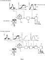
- a voltage waveform before input to the denoising filter 5 and a voltage waveform after output from the denoising filter 5 are illustrated in Fig. 3 .
- the denoising filter 5 in the present embodiment enables resolution to be improved in both the time direction and the energy direction.
- Fig. 4(A) schematically illustrates signal waveforms at respective points in an X-ray detection system having no denoising filter 5 (conventional example), and (B) of the same drawing schematically illustrates signal waveforms at respective points in the X-ray detection system having the denoising filter 5 (present embodiment).
- the measurement was performed using Mn as a sample under the conditions of an X-ray tube voltage of 15 kV, a tube current of 50 ⁇ A, an irradiation diameter ⁇ of 3mm, a niobium (Nb) filter, and an SDD cooling temperature of -15 °C.
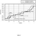
- Fig. 5 illustrates the result of the measurement test.
- Fig. 5 is a spectrum when the filter time constant PT of a pulse processor (slow waveform output part 61) is 50 ns, and the horizontal axis corresponds to 10 eV per channel.
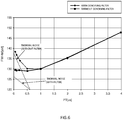
- Fig. 6 illustrates the energy resolution (full width at half maximum (FWHM)) of a Mn-K ⁇ spectrum at each filter time constant PT in the presence or absence of the denoising filter 5.
- the denoising filter 5 provided in the stage prior to the waveform shaping part 6 takes the weighted moving average of the values of the digital voltage signal using a weighting factor w(t, k) depending on the difference from the predetermined reference value v(t), and therefore the noise of the digital voltage signal to be inputted to the waveform shaping part 6 can be removed.
- the noise can be removed while smoothing the step parts of the digital voltage signal to be inputted to the slow waveform output part 61 and preventing dulling, and the X-ray energy resolution can be improved.
- a process time by the slow waveform output part 61 can be more shortened to reduce the probability of the incidence of multiple X-rays within the process time, thus reducing the occurrence of a pile-up.
- the filter time constant PT of the fast waveform output part 62 can be more decreased, and also the pulse detection threshold value can be reduced to the lower energy side, even in the case of incidence of lower energy X-rays, closely incident X-rays can be separated.
- pulse detection can be performed in the lower energy region by the fast waveform output part 62.
- pile-up detection can be performed at the best time resolution. That is, even when the filter time constant PT is set to 10 ns and the pulse detection threshold value is set to 400 eV or less, noise is not erroneously detected.
- the above-described embodiment is one using the rectangular-shaped weighting factor (0 or 1) depending on the value of the digital voltage signal; however, the following one is also possible.
- a weighting factor exhibiting Gaussian characteristics is also possible depending on the difference from the reference value or a weighting factor inversely proportional (monotonic decrease) to the difference from the reference value is also possible.
- the weighting factor is basically decreased with distance from the reference value in the voltage direction, it is not simply decreased, but may be constant or partially increased.
- the denoising filter 5 may be one adapted to take the weighted moving average also in the time direction in addition to the weighted moving average in the voltage direction. That is, the denoising filter 5 takes the weighted moving average of the values of the digital voltage signal using a weighting factor w'(t) depending on the time difference from the time point t 0 corresponding to the reference value v(t 0 ). Specifically, the denoising filter 5 takes the weighted moving average of the voltage values v(t) using the weighting factor w'(t) depending on
- the denoising filter 5 is desirably configured so that as the difference from the time point t 0 corresponding to the reference value v(t 0 ) increases, the weighting factor w'(t) decreases. It is conceivable that the weighting factor w'(t) is set in the same manner as the weighting factor w(t) in the voltage direction.
- a configuration adapted to provide a bypass path that bypasses the denoising filter 5, and be switchable between path through which the digital voltage signal reaches the waveform shaping part 6 from the A/D conversion part 4 via the denoising filter 5 and a path through which the digital voltage signal reaches the waveform shaping part 6 from the A/D conversion part 4 without denoising filter 5 is also possible.
- a configuration having multiple denoising filters 5 is also possible, and a configuration adapted to serially arrange filters having different parameters such as filter threshold values and filter intervals (filter lengths) or to parallel arrange them and make a switch is also possible.
- the slow waveform output part 61 and the fast waveform output part 62 may be respectively provided with denoising filters.
- the denoising filter 5 is provided between the A/D conversion part 4 and the waveform shaping part 6, but not limited to this.
- the waveform shaping part 6 may be provided with the denoising filter 5 to remove noise simultaneously with waveform shaping or to remove noise after waveform shaping.
- the denoising filter 5 may be provided between the waveform shaping part 6 and the pulse height detection part 7 to remove noise of a pulse signal outputted from the waveform shaping part 6.
- a signal processor for radiation detection of the present invention may be one having none of the waveform shaping part, pulse height detection part, and count part.
- an information processor separately from the signal processor, an information processor having the waveform shaping part, pulse height detection part, and count part is provide.
- this signal processor for radiation detection is one including: a preamplifier that converts charge outputted from a radiation detector on which radiation is incident into an analog signal; an A/D conversion part that converts the analog signal from the preamplifier into a digital signal; and a denoising filter that removes noise from the digital signal from the A/D conversion part, in which the denoising filter removes the noise by taking the weighted moving average of values of the digital signal using a weighting factor depending on the difference from a predetermined reference value.
- the X-ray detector another semiconductor detector such as a Si (Li) type detector can be used, or other than semiconductor is also possible, such as a proportional counter tube or a photomultiplier tube.
- the radiation detector may be of a type that a light detector detects light resulting from conversion by a scintillator or the like.
- the X-ray detection system 100 may be one including a gradient detection part 63 that detects a step-based gradient from a digital voltage signal having passed through a denoising filter 5.
- the function of the denoising filter 5 is the same as in the above-described embodiment.
- the gradient detection part 63 is provided separately from a slow waveform output part 61 and a fast waveform output part 62, and configured to include a digital pulse processor (DPP).
- the gradient detection part 63 is a filter that performs waveform shaping to decrease voltages other than at steps to base voltage while keeping the gradients of step parts of the digital voltage signal.
- the denoising filter 5 provided in the stage prior to the gradient detection part 63 takes the weighted moving average of the values of the digital voltage signal using a weighting factor depending on the difference from a predetermined reference value, thus making it easy to determine the rise of a step part due to the incidence of an X-ray in the gradient detection part 63, so that from the slope (gradient) of the rise, the incident position of the X-ray in an X-ray detector 2 can be estimated, and a pile-up caused by the incidence of multiple X-rays can be detected.
- the silicon drift detector in the above-described embodiment may be one in which as illustrated in Fig. 8 , an X-ray detection area is divided into more than one, and each area is provided with a collecting electrode (anode).
- the strength of an electric field is weak, and a distance to a collecting electrode is long, so that it takes time for generated electrons to be collected by a collecting electrode.
- a detection signal caused by electrons generated at the boundary exhibits a slower change in signal value with respect to time than a detection signal caused by electrons generated in an area other than it.
- the pulse processor (such as the gradient detection part 63) may be configured to determine whether the slope of a voltage signal is a predetermined value or less, and when it is equal to or less than the predetermined value, remove the voltage signal on the assumption that the voltage signal is caused by an X-ray incident on a boundary. Since the voltage signal whose noise has been removed by the denoising filter 5 is used to determine whether or not the slope thereof is predetermined value or less, the determination can be accurately made.
- the radiation detection system is capable of reducing white noise to improve radiation energy resolution, as well as improve pulse detection time resolution.
Landscapes
- Physics & Mathematics (AREA)
- Health & Medical Sciences (AREA)
- Life Sciences & Earth Sciences (AREA)
- General Physics & Mathematics (AREA)
- High Energy & Nuclear Physics (AREA)
- Molecular Biology (AREA)
- Spectroscopy & Molecular Physics (AREA)
- Measurement Of Radiation (AREA)
Applications Claiming Priority (2)
| Application Number | Priority Date | Filing Date | Title |
|---|---|---|---|
| JP2016091716 | 2016-04-28 | ||
| PCT/JP2017/014864 WO2017187972A1 (ja) | 2016-04-28 | 2017-04-11 | 放射線検出装置及び放射線検出用信号処理装置 |
Publications (3)
| Publication Number | Publication Date |
|---|---|
| EP3451024A1 true EP3451024A1 (de) | 2019-03-06 |
| EP3451024A4 EP3451024A4 (de) | 2019-12-11 |
| EP3451024B1 EP3451024B1 (de) | 2026-03-04 |
Family
ID=60160510
Family Applications (1)
| Application Number | Title | Priority Date | Filing Date |
|---|---|---|---|
| EP17789259.3A Active EP3451024B1 (de) | 2016-04-28 | 2017-04-11 | Strahlungsdetektor und signalprozessor zur strahlungsdetektion |
Country Status (4)
| Country | Link |
|---|---|
| US (1) | US10795031B2 (de) |
| EP (1) | EP3451024B1 (de) |
| JP (1) | JP6857174B2 (de) |
| WO (1) | WO2017187972A1 (de) |
Families Citing this family (9)
| Publication number | Priority date | Publication date | Assignee | Title |
|---|---|---|---|---|
| JP6628701B2 (ja) * | 2016-08-05 | 2020-01-15 | 三菱電機株式会社 | 放射線測定装置 |
| DE102019104710B4 (de) * | 2019-02-25 | 2023-04-27 | Ketek Gmbh | Verfahren zum Betreiben eines Strahlungsdetektionssystems und Strahlungsdetektionssystem |
| JP7079748B2 (ja) * | 2019-03-14 | 2022-06-02 | 株式会社堀場製作所 | 放射線検出装置及び放射線検出用信号処理装置 |
| CN111431494B (zh) * | 2020-04-15 | 2023-04-11 | 中国科学院国家空间科学中心 | 一种具有数字控制接口的多路小型电荷灵敏放大系统 |
| US12019037B2 (en) | 2020-04-27 | 2024-06-25 | Horiba, Ltd. | Signal processing method, learning model generation method, signal processing device, radiation detecting device, and recording medium |
| JP7624899B2 (ja) * | 2021-08-13 | 2025-01-31 | 株式会社堀場製作所 | 信号処理方法、放射線検出装置及びコンピュータプログラム |
| JP7218958B1 (ja) | 2021-08-24 | 2023-02-07 | 株式会社リガク | X線分析装置及び波高値予測プログラム |
| CN114063139B (zh) * | 2021-11-23 | 2025-02-18 | 中国科学院电工研究所 | 一种数字多道脉冲幅度分析装置 |
| US12411253B1 (en) * | 2022-11-14 | 2025-09-09 | Ut-Battelle, Llc | Pulse shape discrimination system for high density imaging |
Family Cites Families (8)
| Publication number | Priority date | Publication date | Assignee | Title |
|---|---|---|---|---|
| US5349193A (en) | 1993-05-20 | 1994-09-20 | Princeton Gamma Tech, Inc. | Highly sensitive nuclear spectrometer apparatus and method |
| US7966155B2 (en) * | 2004-06-04 | 2011-06-21 | William K. Warburton | Method and apparatus for improving detection limits in x-ray and nuclear spectroscopy systems |
| CA2732754C (en) * | 2007-08-03 | 2015-12-08 | Pulsetor, Llc | Digital pulse processor slope correction |
| JP5071813B2 (ja) * | 2009-01-26 | 2012-11-14 | 応用光研工業株式会社 | 放射線量測定方法と放射線量測定装置 |
| JP2013186109A (ja) * | 2012-03-12 | 2013-09-19 | Panasonic Corp | 放射線量測定システム、並びにそれに用いるデータ収集装置及び測定局 |
| JP6124663B2 (ja) * | 2013-04-19 | 2017-05-10 | 三菱電機株式会社 | 線量率測定装置 |
| JP6159144B2 (ja) | 2013-05-10 | 2017-07-05 | 株式会社堀場製作所 | パルス波高検出装置、放射線検出装置、放射線分析装置、及びパルス波高検出方法 |
| KR101672874B1 (ko) | 2014-04-17 | 2016-11-29 | 아주대학교산학협력단 | 휴대용 방사선 검출장치 및 그 방법 |
-
2017
- 2017-04-11 EP EP17789259.3A patent/EP3451024B1/de active Active
- 2017-04-11 WO PCT/JP2017/014864 patent/WO2017187972A1/ja not_active Ceased
- 2017-04-11 US US16/097,053 patent/US10795031B2/en active Active
- 2017-04-11 JP JP2018514250A patent/JP6857174B2/ja active Active
Also Published As
| Publication number | Publication date |
|---|---|
| JP6857174B2 (ja) | 2021-04-14 |
| EP3451024B1 (de) | 2026-03-04 |
| WO2017187972A1 (ja) | 2017-11-02 |
| US10795031B2 (en) | 2020-10-06 |
| JPWO2017187972A1 (ja) | 2019-02-28 |
| US20190154847A1 (en) | 2019-05-23 |
| EP3451024A4 (de) | 2019-12-11 |
Similar Documents
| Publication | Publication Date | Title |
|---|---|---|
| EP3451024B1 (de) | Strahlungsdetektor und signalprozessor zur strahlungsdetektion | |
| EP2183578B1 (de) | Stapelungszurückweisung in einem energiedispersiven strahlenspektrometriesystem | |
| CA2732522C (en) | Pileup rejection in an energy-dispersive radiation spectrometry system | |
| JP5611357B2 (ja) | 放射線計測装置 | |
| CN110308476B (zh) | 一种粒子辐射探测方法及探测装置 | |
| CN107817514B (zh) | 一种数字化核能谱测量系统中的脉冲阶梯成形方法 | |
| US20130275054A1 (en) | System and method of extending the linear dynamic range of event counting | |
| Hammad et al. | Pile-up correction algorithm for high count rate gamma ray spectroscopy | |
| CN107783173A (zh) | 一种数字化核能谱测量系统中的脉冲矩形成形方法 | |
| US10641909B2 (en) | Method for processing a pulse generated by a detector of ionizing radiation | |
| JP6159144B2 (ja) | パルス波高検出装置、放射線検出装置、放射線分析装置、及びパルス波高検出方法 | |
| EP3264138B1 (de) | Labr3-szintillationsdetektor und verfahren zur entfernung spezifischer ereignisse | |
| JP7079748B2 (ja) | 放射線検出装置及び放射線検出用信号処理装置 | |
| US11397270B2 (en) | Method for operating a signal filter and radiation detection system | |
| JP6999593B2 (ja) | 検出装置及びスペクトル生成装置 | |
| JP6813572B2 (ja) | 放射線検出装置及び放射線検出用信号処理装置 | |
| CN109491960B (zh) | 一种减小图像畸变的位置读出电路 | |
| Johnson et al. | High event rate, pulse shape discrimination algorithm for CLYC | |
| Kumar Paul et al. | Implementation of FPGA based real-time digital DAQ for high resolution, and high count rate nuclear spectroscopy application | |
| US11194061B2 (en) | Optical detector and optical detection device | |
| Mott | Improved coincidence rejection for silicon drift detectors |
Legal Events
| Date | Code | Title | Description |
|---|---|---|---|
| STAA | Information on the status of an ep patent application or granted ep patent |
Free format text: STATUS: THE INTERNATIONAL PUBLICATION HAS BEEN MADE |
|
| PUAI | Public reference made under article 153(3) epc to a published international application that has entered the european phase |
Free format text: ORIGINAL CODE: 0009012 |
|
| STAA | Information on the status of an ep patent application or granted ep patent |
Free format text: STATUS: REQUEST FOR EXAMINATION WAS MADE |
|
| 17P | Request for examination filed |
Effective date: 20181106 |
|
| AK | Designated contracting states |
Kind code of ref document: A1 Designated state(s): AL AT BE BG CH CY CZ DE DK EE ES FI FR GB GR HR HU IE IS IT LI LT LU LV MC MK MT NL NO PL PT RO RS SE SI SK SM TR |
|
| AX | Request for extension of the european patent |
Extension state: BA ME |
|
| DAV | Request for validation of the european patent (deleted) | ||
| DAX | Request for extension of the european patent (deleted) | ||
| A4 | Supplementary search report drawn up and despatched |
Effective date: 20191113 |
|
| RIC1 | Information provided on ipc code assigned before grant |
Ipc: G01T 1/17 20060101AFI20191107BHEP |
|
| STAA | Information on the status of an ep patent application or granted ep patent |
Free format text: STATUS: EXAMINATION IS IN PROGRESS |
|
| 17Q | First examination report despatched |
Effective date: 20211122 |
|
| P01 | Opt-out of the competence of the unified patent court (upc) registered |
Effective date: 20231108 |
|
| GRAP | Despatch of communication of intention to grant a patent |
Free format text: ORIGINAL CODE: EPIDOSNIGR1 |
|
| STAA | Information on the status of an ep patent application or granted ep patent |
Free format text: STATUS: GRANT OF PATENT IS INTENDED |
|
| INTG | Intention to grant announced |
Effective date: 20251006 |
|
| GRAS | Grant fee paid |
Free format text: ORIGINAL CODE: EPIDOSNIGR3 |
|
| GRAA | (expected) grant |
Free format text: ORIGINAL CODE: 0009210 |
|
| STAA | Information on the status of an ep patent application or granted ep patent |
Free format text: STATUS: THE PATENT HAS BEEN GRANTED |
|
| AK | Designated contracting states |
Kind code of ref document: B1 Designated state(s): AL AT BE BG CH CY CZ DE DK EE ES FI FR GB GR HR HU IE IS IT LI LT LU LV MC MK MT NL NO PL PT RO RS SE SI SK SM TR |
|
| REG | Reference to a national code |
Ref country code: CH Ref legal event code: F10 Free format text: ST27 STATUS EVENT CODE: U-0-0-F10-F00 (AS PROVIDED BY THE NATIONAL OFFICE) Effective date: 20260304 Ref country code: GB Ref legal event code: FG4D |
|
| REG | Reference to a national code |
Ref country code: IE Ref legal event code: FG4D |
|
| REG | Reference to a national code |
Ref country code: DE Ref legal event code: R096 Ref document number: 602017094156 Country of ref document: DE |