EP3444643B1 - Multi-level diffractive optical element thin film coating - Google Patents
Multi-level diffractive optical element thin film coating Download PDFInfo
- Publication number
- EP3444643B1 EP3444643B1 EP18188469.3A EP18188469A EP3444643B1 EP 3444643 B1 EP3444643 B1 EP 3444643B1 EP 18188469 A EP18188469 A EP 18188469A EP 3444643 B1 EP3444643 B1 EP 3444643B1
- Authority
- EP
- European Patent Office
- Prior art keywords
- reflectance
- layer
- reflectance structure
- optical element
- diffractive optical
- Prior art date
- Legal status (The legal status is an assumption and is not a legal conclusion. Google has not performed a legal analysis and makes no representation as to the accuracy of the status listed.)
- Active
Links
Images


Classifications
-
- G—PHYSICS
- G02—OPTICS
- G02B—OPTICAL ELEMENTS, SYSTEMS OR APPARATUS
- G02B5/00—Optical elements other than lenses
- G02B5/18—Diffraction gratings
- G02B5/1866—Transmission gratings characterised by their structure, e.g. step profile, contours of substrate or grooves, pitch variations, materials
-
- G—PHYSICS
- G02—OPTICS
- G02B—OPTICAL ELEMENTS, SYSTEMS OR APPARATUS
- G02B1/00—Optical elements characterised by the material of which they are made; Optical coatings for optical elements
- G02B1/10—Optical coatings produced by application to, or surface treatment of, optical elements
-
- G—PHYSICS
- G02—OPTICS
- G02B—OPTICAL ELEMENTS, SYSTEMS OR APPARATUS
- G02B1/00—Optical elements characterised by the material of which they are made; Optical coatings for optical elements
- G02B1/10—Optical coatings produced by application to, or surface treatment of, optical elements
- G02B1/11—Anti-reflection coatings
- G02B1/113—Anti-reflection coatings using inorganic layer materials only
- G02B1/115—Multilayers
-
- G—PHYSICS
- G02—OPTICS
- G02B—OPTICAL ELEMENTS, SYSTEMS OR APPARATUS
- G02B27/00—Optical systems or apparatus not provided for by any of the groups G02B1/00 - G02B26/00, G02B30/00
- G02B27/42—Diffraction optics, i.e. systems including a diffractive element being designed for providing a diffractive effect
- G02B27/44—Grating systems; Zone plate systems
-
- G—PHYSICS
- G02—OPTICS
- G02B—OPTICAL ELEMENTS, SYSTEMS OR APPARATUS
- G02B5/00—Optical elements other than lenses
- G02B5/18—Diffraction gratings
-
- G—PHYSICS
- G02—OPTICS
- G02B—OPTICAL ELEMENTS, SYSTEMS OR APPARATUS
- G02B5/00—Optical elements other than lenses
- G02B5/18—Diffraction gratings
- G02B5/1847—Manufacturing methods
- G02B5/1857—Manufacturing methods using exposure or etching means, e.g. holography, photolithography, exposure to electron or ion beams
-
- G—PHYSICS
- G02—OPTICS
- G02B—OPTICAL ELEMENTS, SYSTEMS OR APPARATUS
- G02B5/00—Optical elements other than lenses
- G02B5/18—Diffraction gratings
- G02B5/1866—Transmission gratings characterised by their structure, e.g. step profile, contours of substrate or grooves, pitch variations, materials
- G02B5/1871—Transmissive phase gratings
-
- G—PHYSICS
- G02—OPTICS
- G02B—OPTICAL ELEMENTS, SYSTEMS OR APPARATUS
- G02B5/00—Optical elements other than lenses
- G02B5/20—Filters
-
- G—PHYSICS
- G02—OPTICS
- G02B—OPTICAL ELEMENTS, SYSTEMS OR APPARATUS
- G02B5/00—Optical elements other than lenses
- G02B5/18—Diffraction gratings
- G02B2005/1804—Transmission gratings
-
- G—PHYSICS
- G02—OPTICS
- G02B—OPTICAL ELEMENTS, SYSTEMS OR APPARATUS
- G02B27/00—Optical systems or apparatus not provided for by any of the groups G02B1/00 - G02B26/00, G02B30/00
- G02B27/10—Beam splitting or combining systems
- G02B27/1086—Beam splitting or combining systems operating by diffraction only
- G02B27/1093—Beam splitting or combining systems operating by diffraction only for use with monochromatic radiation only, e.g. devices for splitting a single laser source
-
- G—PHYSICS
- G02—OPTICS
- G02B—OPTICAL ELEMENTS, SYSTEMS OR APPARATUS
- G02B27/00—Optical systems or apparatus not provided for by any of the groups G02B1/00 - G02B26/00, G02B30/00
- G02B27/42—Diffraction optics, i.e. systems including a diffractive element being designed for providing a diffractive effect
- G02B27/4272—Diffraction optics, i.e. systems including a diffractive element being designed for providing a diffractive effect having plural diffractive elements positioned sequentially along the optical path
Definitions
- the present disclosure relates to thin film structures. More particularly, some aspects of the present disclosure relate to a multi-level thin film structure for a diffractive optical element (DOE) that provides a particular phase delay between an etched region and an un-etched region of the multi-layer thin film structure, and that provides anti-reflectance for a particular wavelength range.
- DOE diffractive optical element
- a multi-level diffractive optical element having anti reflection functionality is disclosed in the german patent publication DE-A1-102005020944 .
- a diffractive optical element may be used for directing a beam.
- a DOE such as a diffractive lens, a spot array illuminator, a spot array generator, a Fourier array generator, and/or the like, may be used to split a beam, shape a beam, focus a beam, and/or the like.
- a DOE may be integrated into a multicast switch, a wavelength selective switch, a gesture recognition system, a motion sensing system, a depth sensing system, and/or the like.
- a two-level surface relief profile (sometimes termed a "binary surface relief profile”) may be selected for a surface relief DOE.
- the two-level surface relief profile may be selected to approximate a continuous surface relief profile and to enable use of a photolithographic procedure and/or an etching procedure to manufacture the DOE.
- a two-level thin film stack may be used to create a single order binary DOE, such as a diffractive lens, and may be associated with a diffraction efficiency of approximately 40% for a single order binary DOE.
- the two-level thin film stack may be used for a spot array generator, and may provide a symmetrical spot array.
- utilizing a two-level thin film stack may provide an axis of symmetry such that intensity of spots is associated with a 180 degree axis of symmetry.
- Some materials used for DOEs may require a relief depth of greater than a threshold, thereby resulting in a threshold etch time to manufacture the DOE.
- the transmissive surface relief diffractive optical element comprises a first anti-reflectance structure for a particular wavelength range formed on the substrate.
- the transmissive surface relief diffractive optical element comprises a second anti-reflectance structure for the particular wavelength range formed on the first anti - reflectance structure.
- the transmissive surface relief diffractive optical element comprises a third anti-reflectance structure for the particular wavelength range formed on the second anti-reflectance structure.
- the transmissive surface relief diffractive optical element comprises at least one layer disposed between the first anti-reflectance structure and the second anti-reflectance structure or between the second anti-reflectance structure and the third anti-reflectance structure.
- a first relief depth between a first surface of the first anti-reflectance structure and a second surface of the second anti-reflectance structure and a second relief depth between the first surface and a third surface of the third anti-reflectance structure are configured to form the surface relief diffractive optical element associated with a first phase delay and a second phase delay, respectively, for the particular wavelength range.
- the first anti-reflectance structure comprises a first top layer and the second anti-reflectance structure comprises a second top layer, each of the first top layer and the second top layer being an etch stop layer to enable etching to form a phase delay.
- Each of the first anti-reflectance structure including the first top layer, the second anti-reflectance structure including the second top layer, and the third anti-reflectance structure comprises alternating layers of two materials, and thereby forming a three-level relief profile having anti-reflectance structures built into each etched stack of the surface relief diffractive optical element and built into the un-etched stack without requiring additional anti-reflectance coatings or structures on the top surface of the three-level relief profile.
- the first phase delay may be a ⁇ /2 phase delay and the second phase delay may be a ⁇ phase delay.
- the first anti-reflectance structure, the second anti-reflectance structure, and the third anti-reflectance structure may be formed from alternating layers of silicon and silicon dioxide.
- the first anti-reflectance structure and the second anti-reflectance structure may be formed from alternating layers of hydrogenated silicon and silicon dioxide.
- the first anti-reflectance structure may be formed from a first layer of a first material and a second layer of a second material; wherein the at least one layer may be formed from a third layer of the first material; wherein the second anti-reflectance structure may be formed from a fourth layer of the second material and a fifth layer of the first material; and wherein the third anti-reflectance structure may be formed from a sixth layer of the second material and a seventh layer of the first material.
- the first anti-reflectance structure may be formed on a first side of the substrate; and the surface relief diffractive optical element may further comprise: a plurality of other anti-reflectance structures for the particular wavelength range formed on a second side of the substrate.
- the particular wavelength range may be between 930 nanometers and 950 nanometers.
- the particular wavelength range may be between 1540 nanometers and 1560 nanometers.
- a method of forming a transmissive surface relief diffractive optical element providing an anti-reflection functionality in a particular wavelength range comprises depositing a plurality of layers onto a wafer, wherein the depositing forms three or more anti-reflectance structures for the particular wavelength range, each anti-reflectance structure comprising at least one pair of layers, wherein a first anti-reflectance structure, of the three or more anti-reflectance structures, is formed on the wafer and beneath a second anti-reflectance structure of the three or more anti-reflectance structures, and wherein the second anti-reflectance structure is formed beneath a third anti-reflectance structure of the three or more anti-reflectance structures.
- At least one layer is formed between two of the three or more anti-reflectance structures.
- the first anti-reflectance structure comprises a first top layer and the second anti-reflectance structure comprises a second top layer, each of the first top layer and the second top layer being an etch stop layer to enable etching to form a phase delay.
- Each of the first anti-reflectance structure including the first top layer, the second anti-reflectance structure including the second top layer, and the third anti-reflectance structure comprises alternating layers of two materials.
- the method comprises etching a subset of layers of the plurality of layers to form a three or more-level relief profile.
- the three-level relief profile comprises a first relief depth between a first surface of the first anti-reflectance structure and a second surface of the second anti-reflectance structure and a second relief depth between the first surface and a third surface of the third anti-reflectance structure, said first relief depth and said second relief depth being configured to form a surface relief diffractive optical element associated with a first phase delay and a second phase delay, respectively, for the particular wavelength range, the surface relief diffractive optical element being configured to provide an anti-reflectance functionality in the particular wavelength range of incident light and having etched regions and un-etched regions, and thereby forming the three-level relief profile having anti-reflectance structures built into each etched stack of the surface relief diffractive optical element and built into the un-etched stack without requiring additional anti-reflectance coatings or structures on the top surface of the three-level relief profile.
- the method may further comprise: dividing the wafer into a plurality of surface relief diffractive optical elements.
- the plurality of layers may include at least one of: a silicon layer, a silicon dioxide layer, a tantalum pentoxide layer, or a silicon nitride layer.
- the method may further comprise: forming another surface relief diffractive optical element including another three or more stacked anti-reflectance structures on another side of the wafer with the particular phase delay for the particular wavelength range.
- a diffractive optical element may be manufactured using a photolithographic procedure and/or an etching procedure. For example, to approximate a continuous surface relief profile, a two-level surface relief profile may be selected for the DOE, and a surface of the DOE may be etched or patterned to form the two-level surface relief profile. The two-level surface relief profile may be used to create a phase delay for a beam passing through the DOE. For a single order binary DOE, such as a diffractive lens, a diffractive efficiency of approximately 40% may be achieved using the two-level surface relief profile.
- this diffractive efficiency may be less than a threshold for utilization of a DOE in an optical system, such as an optical communications system, a gesture recognition system, a motion detection system, a depth sensing system, and/or the like.
- a spot array pattern or diffraction pattern created by the DOE may be symmetrical, and an asymmetric diffraction pattern may be desired for a particular optical system.
- Some implementations, described herein may provide a multi-level DOE with a threshold diffractive efficiency. For example, some implementations, described herein, provide a multi-level DOE (e.g., greater than two levels) to provide a particular phase delay at a particular wavelength of incident light between portions of the DOE and an anti-reflectance at the particular wavelength of incident light. Moreover, some implementations, described herein, may provide a DOE associated with an asymmetric spot array pattern or diffraction pattern.
- a DOE may be associated with a relief depth to fabricate a selected surface relief profile of less than a threshold, thereby resulting in a reduced aspect ratio, a reduced etch time, and/or a reduced fabrication cost for the DOE (relative to other techniques for manufacturing a DOE).
- layers of the DOE may provide an integrated etch stop for the DOE.
- Some implementations, described herein, may provide a method for manufacturing a DOE. For example, a DOE may be manufactured using a thin film deposition procedure, an etching procedure, and/or the like, which may provide improved layer thickness accuracy and improved manufacturability relative to other techniques for manufacturing a DOE.
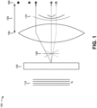
- Fig. 1 is a diagram of an overview of an example implementation 100 described herein.
- Fig. 1 shows an example of spot array generation using a surface relief DOE grating and a converging lens as a spot array illuminator (sometimes termed a spot array generator or dot array generator).
- an incident plane wave 110 is directed toward a surface relief DOE grating 120.
- surface relief DOE grating 120 may be a DOE with a multi-level surface relief profile, such as a four-level DOE, an eight-level DOE, a 2"-level DOE (where n > 1), a k-level DOE (e.g., where k > 2), and/or the like.
- surface relief DOE grating 120 may include, for example, alternating layers of silicon (Si) and silicon dioxide (SiO 2 ), alternating layers of hydrogenated silicon (Si:H) and silicon dioxide, and/or the like.
- layers of surface relief DOE grating 120 are configured to provide an anti-reflectance functionality at a particular wavelength of incident light.
- a layer of surface relief DOE grating 120 e.g., a silicon dioxide layer
- incident plane wave 110 may have a wavelength in a range from approximately 800 nanometers (nm) to approximately 1100 nm, approximately 800 nm to approximately 1000 nm, approximately 830 nm to approximately 1000 nm, approximately 850 nm to approximately 1000 nm, approximately 915 nm to approximately 1000 nm, approximately 940 nm to approximately 1000 nm, approximately 930 nm to approximately 950 nm, and/or the like.
- incident plane wave 110 may have a wavelength in a range from approximately 1100 nm to approximately 2000 nm, approximately 1400 nm to approximately 1700 nm, approximately 1520 nm to approximately 1630 nm, approximately 1540 nm to approximately 1560 nm, and/or the like. Additional details regarding surface relief DOE grating 120 are described herein.
- example implementation 100 may be used for a gesture recognition system, and focal plane 160 may be a target for gesture recognition. Additionally, or alternatively, focal plane 160 may be an object (e.g., for an object sensing system), a communications target (e.g., for an optical communication system), and/or the like.
- wavefront 170 is directed toward focal plane 160 causing a multiple spot array pattern to be formed at focal plane 160.
- the multiple spot array pattern may be asymmetric.
- surface relief DOE grating 120 may be used to create a two-dimensional spot array. In this way, surface relief DOE grating 120 may be used as a spot array illuminator to create a spot array at focal plane 160 from incident plane wave 110, thereby enabling a gesture recognition system, a motion sensing system, an optical communications system, and/or the like.
- Fig. 1 is provided merely as an example. Other examples are possible and may differ from what was described with regard to Fig. 1 .
- Figs. 2A and 2B are diagrams relating to an example implementation described herein. As shown in Fig. 2A , and by diagram 200, a continuous relief profile can be quantized into a set of discrete levels to enable a photolithographic and/or an etching procedure to be used for manufacturing a DOE.
- a continuous relief profile may be associated with a diffractive efficiency of approximately 100% (for a single order configuration) and may provide a continuously increasing phase delay of 2 ⁇ from a second pitch position, dx, relative to a first pitch position, 0.
- the continuous relief profile may be approximated by a two-level relief profile (sometimes termed a binary relief profile).
- the two-level relief profile may be associated with a diffractive efficiency of approximately 40.5% (for a single order configuration) and may provide a ⁇ phase delay at a second region of a DOE, from pitch position 0.5dx to pitch position dx, relative to a first region of the DOE, from pitch position 0 to pitch position 0.5dx.
- the continuous relief profile may be approximated by a 4-level relief profile.
- the 4-level relief profile may be associated with a diffractive efficiency of approximately 81% (for a single order configuration), and may provide a ⁇ /2 phase delay at a second region of the DOE, from pitch position 0.25dx to pitch position 0.5dx, relative to a first region of the DOE, from 0 to 0.25dx ; a ⁇ phase delay at a third region of the DOE, from 0.5dx to 0.75dx, relative to the first region of the DOE; and a 3 ⁇ /2 phase delay at a fourth region of the DOE, from 0.75dx to dx, relative to the first region of the DOE.
- the continuous relief profile may be approximated by an 8-level relief profile.
- the 8-level relief profile may be associated with a diffractive efficiency of approximately 95% (for a single order configuration), and may provide phase delays in increments of ⁇ /4 at regions of the DOE (e.g., ⁇ /4 at a second region from 0.125dx to 0.25dx ; ⁇ /2 at a third region, from 0.25dx to 0.375dx ; 3 ⁇ /4 at a fourth region, from 0.375dx to 0.5dx ; etc. relative to a first region of the DOE, from 0 to 0.125dx ).
- another configuration with another diffraction efficiency may be used.
- a configuration using 2 orders, 4 orders, 10 orders, 100 orders, and/or the like may be used to increase a diffraction efficiency relative to the single order configuration.
- a diffraction efficiency of approximately 75% to 80% may be achieved for a two-level relief profile.
- diffractive efficiency may be improved to greater than a threshold (for a single order configuration and/or the like), such as greater than 41%, greater than 50%, greater than 75%, greater than 80%, greater than 85%, greater than 90%, greater than 95%, greater than 99%, and/or the like.
- n > 1 e.g., a 4-level DOE, an 8-level DOE, etc.
- k > 2 e.g., a 3-level DOE, a 5-level DOE, a 6-level DOE, etc.
- k > 2 e.g., a 4-level DOE, an 8-level DOE, etc.
- a multi-level DOE may enable additional quantities of phase delays and/or values of phase delays.
- a DOE 210 may include a substrate 215.
- substrate 215 may be a glass substrate, a fused silica substrate, and/or the like.
- substrate 215 may be a fused silica substrate with a thickness of approximately 200 micrometers, and with a refractive index, n sub , of 1.45.
- a set of alternating silicon and silicon dioxide layers may be disposed onto a top surface of substrate 215 and patterned to form a relief profile, as described herein, and anti-reflectance coating 220 may cover the bottom surface of substrate 215.
- anti-reflectance coating 220 may be absent or may be substituted with another anti-reflectance structure such as the anti-reflectance structure formed on the top surface.
- an anti-reflectance structure may include a thin film, a thin film structure, an anti-reflectance coating, a deposited thin layer, a deposited thin film layer, and/or the like.
- the set of alternating silicon and silicon dioxide layers may include a set of silicon layers 225 and a set of silicon dioxide layers 230.
- silicon layer 225-1 may be disposed on substrate 215, and silicon dioxide layer 230-1 may be disposed on silicon layer 225-1.
- Silicon layer 225-1 and silicon dioxide layer 230-1 may form a pair of matched layers 235-1, which provide a first anti-reflectance structure.
- silicon dioxide layer 230-2 may be disposed on silicon layer 225-2, and may form a pair of matched layers 235-2, which provide a second anti-reflectance structure; silicon dioxide layer 230-3 may be disposed on silicon layer 225-3, and may form a pair of matched layers 235-3, which provide a third anti-reflectance structure; silicon layer 225-4 may be disposed on silicon dioxide layer 230-4, and may form a pair of matched layers 235-4, which provide a fourth anti-reflectance structure. As shown, silicon layer 225-5 may be disposed between matched layers 235-3 and matched layers 235-4. Silicon layer 225-5 may be configured to provide a particular functionality for DOE 210, and may be configured independent of the anti-reflectance structures, thereby improving flexibility in DOE design.
- DOE 210 may be exposed to an air or gaseous interface.
- a first surface of DOE 210 e.g., surfaces of matched layers 235
- a second surface of DOE 210 e.g., a surface of anti-reflectance coating 220
- n air refractive index
- a material with a relatively large refractive index may be selected, such as silicon dioxide, which may result, in some implementations, in a relief depth, h, of an etch (e.g., etch 240) of approximately 0.75 micrometers ( ⁇ m).
- the relief depth may be a relief depth of between 0.4 ⁇ m and 3.0 ⁇ m, between 0.5 ⁇ m and 2.5 ⁇ m, between 1.0 ⁇ m and 2.0 ⁇ m, and/or the like.
- layers may be index matched to increase transmittance of DOE 210.
- silicon layers 225 and silicon dioxide layers 230 may be selected based on respective refractive indices of 3.5 and 1.45 being within a threshold amount of between 1.4 and 3.9.
- other materials may be selected for a thin film coating material, such as tantalum pentoxide (Ta 2 O 5 ) and silicon nitride (Si 3 N 4 ), which may have a refractive index of approximately 2.0. Based on using silicon thin film for layers of DOE 210, a relief depth for a 4-level relief profile is reduced relative to other material selections.
- a thin film coating material such as tantalum pentoxide (Ta 2 O 5 ) and silicon nitride (Si 3 N 4 ), which may have a refractive index of approximately 2.0.
- silicon dioxide may be associated with a relief depth of approximately 2.33 ⁇ m
- tantalum pentoxide and silicon nitride may be associated with a relief depth of approximately 1.16 ⁇ m
- silicon may be associated with a relief depth of approximately 0.47 ⁇ m.
- Other materials with similar refractive indices such as a refractive index range of between 1.5 and 3.5, a refractive index of 2.0, and/or the like may be used.
- silicon dioxide may be associated with a relief depth of approximately 2.71 ⁇ m
- tantalum pentoxide and silicon nitride may be associated with a relief depth of approximately 1.36 ⁇ m
- silicon may be associated with a relief depth of approximately 0.54 ⁇ m.
- hydrogenation may be used to improve optical performance of a coating material.
- hydrogenated silicon may be used for silicon layers 225. In this way, hydrogenation may be used to reduce an absorption edge of silicon to enable use for a wavelength of between 800 nm and 1000 nm and to reduce the desired relief depth of the DOE to improve manufacturing (e.g. increase quality and/or yield).
- Argon may be used in a deposition chamber to form a low absorption coating (e.g., less than a threshold amount of absorption).
- a silicon carbide may be used with a refractive index of approximately 2.7 for use with visible light wavelengths and/or the like, such as for a DOE lens for a camera.
- FIGS. 2A and 2B are provided merely as examples. Other examples are possible and may differ from what was described with regard to Figs. 2A and 2B .
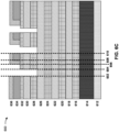
- Figs. 3A and 3B are diagrams of example implementations of DOEs 300 and 300'.
- DOE 300 includes a substrate 305, an anti-reflectance coating 310, a set of silicon layers 315-1 through 315-4, and a set of silicon dioxide layers 320-1 through 320-3.
- silicon dioxide layers 320-1 and 320-2 may be etch stop layers to enable etching to more accurately form a 2 ⁇ (K-1)/K phase delay for a quantity of levels K.
- an etching procedure may be performed such that un-etched stack 330 remains un-etched and etched stacks 335-1 and 335-2 are etched to relief depths 340-1 and 340-2, respectively.
- Relief depth 340-1 may provide a 2 ⁇ (K-1)/K phase delay between etched stack 335-1 and un-etched stack 330.
- Relief depth 340-2 may provide a phase delay between 0 and 2 ⁇ /K between etched stack 335-2 and un-etched stack 330.
- DOE 300 may be manufactured using multiple silicon dioxide etch tools, multiple silicon etch tools, multiple etching techniques (e.g., a deep reactive ion (DRIE) etch tool technique, a reactive-ion etching (RIE) tool technique, a sputter etching tool technique, and/or the like), and/or the like.
- DRIE deep reactive ion
- RIE reactive-ion etching
- layers of DOE 300 may form a set of anti-reflectance structures.
- layers 320-1 and 315-1 form a first anti-reflectance structure for a particular wavelength range (e.g. the wavelength of incident light)
- layers 315-2 and 320-2 may form a second anti-reflectance structure for the particular wavelength range
- layers 315-3 and 320-3 form a third anti-reflectance structure for the particular wavelength range, thereby forming a three-level relief profile having anti-reflectance structures built into each etched stack of the DOE 300 and built into the un-etched stack 330. Accordingly, the DOE 300 does not require additional anti-reflectance coatings or structures on the top surface.
- the second anti-reflectance structure may be formed on the first anti-reflectance structure, and an adjacent surface of the first anti-reflectance structure (e.g., a top surface of layer 320-1) may be an etch stop for etching to form etched stack 335-1.
- the third anti-reflectance structure may be formed on the second anti-reflectance structure, and an adjacent surface the second anti-reflectance structure (e.g., a top surface of layer 320-2) may be an etch stop when forming etched stack 335-2.
- At least one layer may be between a set of anti-reflectance structures (e.g., between the first anti-reflectance structure and the second anti-reflectance structure, between the second anti-reflectance structure and the third anti-reflectance structure, and/or the like).
- a set of anti-reflectance structures e.g., between the first anti-reflectance structure and the second anti-reflectance structure, between the second anti-reflectance structure and the third anti-reflectance structure, and/or the like.
- an alteration to the relief depths 340-1 and/or 340-2 may be performed to alter a characteristic of DOE 300 without altering transmission characteristics of DOE 300.
- the first anti-reflectance structure, the second anti-reflectance structure, and/or the third anti-reflectance structure may not be separated by a layer.
- each layer may be associated with a particular thickness.
- the particular thickness may correspond to a wavelength of light for which the particular phase delay is caused and for which DOE 300 is transmissive (e.g., greater than a threshold percentage of transmissivity, such as greater than 99%, greater than 98%, greater than 97%, greater than 95%, greater than 90%, and/or the like).
- DOE 300 may be associated with a particular pitch 345 (sometimes termed a period), dx, which may correspond to a wavelength of light for which the particular phase delay is caused and for which DOE 300 is transmissive.
- a capping layer may be formed onto the seventh layer (e.g., another silicon dioxide layer), which may improve robustness during dicing of a wafer that includes DOE 300.
- thicknesses of layers of DOE 300, a size of pitch 345, an index of refraction of the anti-reflectance structures and/or the layers thereof, and/or the like may be selected to cause a particular phase delay (e.g., the 2 ⁇ (K-1)/K phase delay) at a particular wavelength for which the anti-reflectance structures provide an anti-reflectance functionality.
- a particular phase delay e.g., the 2 ⁇ (K-1)/K phase delay
- the first anti-reflectance structure may be associated with a first index of refraction of a particular amount
- the second anti-reflectance structure may be associated with a second index of refraction of 3.4
- the third anti-reflectance structure may be associated with a third index of refraction of 2.81 for a 940 nm three level thin film DOE.
- the particular wavelength may include a wavelength range of between approximately 1530 nm and 1570 nm, 930 nm to 950 nm, and/or the like.
- a set of intensity orders e.g., intensity orders -2, -1, 0, 1, 2, etc.
- DOE 300 may provide greater than 50 intensity orders, greater than 100 intensity orders, greater than 200 intensity orders, greater than 300 intensity orders, greater than 350 intensity orders, greater than 500 intensity orders, and/or the like.
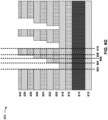
- DOE 300' includes a first diffractive (transmissive) optical element formed on a first side of substrate 305 and a second diffractive (transmissive) optical element formed on a second side of substrate 305.
- Each diffractive optical element includes a set of silicon layers 315-1 through 315-4 and a set of silicon dioxide layers 320-1 through 320-3.
- the second diffractive optical element based on incident light being directed toward DOE 300', causes a first set of intensity orders to be directed through substrate 305 to the first diffractive optical element, which causes a second set of intensity orders to be provided from DOE 300'.
- substrate 305 maintains an alignment of the first diffractive optical element and the second diffractive optical element, thereby reducing a difficulty in maintaining alignment relative to another technique, such as free space optics or using a pick-and-place machine to independently align two separate DOEs.
- another technique such as free space optics or using a pick-and-place machine to independently align two separate DOEs.
- an amount of mechanical stress may be balanced for the DOEs, thereby improving durability, increasing flatness of the DOEs across operating temperature ranges, reducing warping or bowing of the DOEs, and/or the like.
- layers such as 7 layers
- other quantities of layers are possible, such as 8 layers (e.g., 8 alternating silicon/silicon dioxide layers), 9 layers, 10 layers, 20 layers, and/or the like.
- FIGS. 3A and 3B are provided merely as examples. Other examples are possible and may differ from what was described with regard to Figs. 3A and 3B .
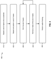
- Fig. 4 is a flow chart of an example process 400 for manufacturing a DOE. Examples of some manufacturing steps of process 400 are shown in more detail with regard to Figs. 5A-5E and Figs. 6A-6G .
- process 400 may include depositing a set of layers onto a substrate (block 410).
- a deposition procedure may be used to deposit the set of layers onto the substrate.
- one or more of the set of layers may be a thin film deposited using a thin film deposition procedure, such as a sputter deposition procedure using a pulsed magnetron sputtering system.
- the set of layers may a set of silicon layers, a set of silicon dioxide layers, and/or the like.
- the set of layers may be deposited onto the substrate with a threshold tolerance.
- the set of layers may be deposited within 2% of a specified thickness, within 1% of a specified thickness, within 0.5% of a specified thickness, within 0.25% of a specified thickness, within 0.1% of a specified thickness, within 0.01% of a specified thickness, and/or the like.
- layers for forming a first anti-reflectance structure for a particular wavelength, a second anti-reflectance structure for the particular wavelength, ... , and an nth anti-reflectance structure for the particular wavelength may be deposited.
- the high accuracy in thickness when depositing thin film coatings may improve accuracy in the relief depth(s) of a DOE.
- the substrate may be a glass substrate, a fused silica substrate, a substrate that is transparent for a particular wavelength of incident light, and/or the like.
- the set of layers may include multiple sets of silicon and silicon dioxide layers. For example, for a 4-level DOE, a first set of silicon and silicon dioxide layers may be deposited onto the substrate, a second set of silicon and silicon dioxide layers may be deposited onto the first set, a third set of silicon and silicon dioxide layers may be deposited onto the second set, and a fourth set of silicon and silicon dioxide layers may be deposited onto the third set.
- another silicon layer may be deposited onto the fourth set, and a set of three mask layers may be deposited onto the other silicon layer, as described in more detail herein, to enable etching and mask removal to form the 4-level DOE.
- other quantities of DOE levels may be possible, such as a 2-level DOE, a 3-level DOE, a 5-level DOE, a 6-level DOE, and/or the like.
- an anti-reflectance coating layer may be formed using the set of layers.
- the anti-reflectance coating may be a DOE anti-reflectance coating to stress balance the substrate and the DOEs, thereby reducing warping of the substrate over an operating temperature range.
- an anti-reflectance layer may be deposited on a back side of the substrate (and layers to form a DOE may be deposited on a front side of the substrate).
- the set of layers may be deposited onto multiple sides of the substrate.
- the set of layers may be deposited to form anti-reflectance structures on a first side of the substrate and on a second side of the substrate, which may result in the substrate supporting multiple DOEs.
- another set of materials may be used for at least one of the layers, such as a hydrogenated silicon based material, a tantalum pentoxide based material, a silicon nitride based material, and/or the like.
- process 400 may include depositing a set of masks onto a surface of the set of layers (block 420).
- a deposition procedure may be used to deposit the set of masks onto surfaces of the set of layers.
- multiple masks may be deposited.
- a first mask may be deposited onto a portion of a top layer of the set of layers
- a second mask may be deposited onto a portion of the top layer and onto the first mask
- a third mask may be deposited onto a portion of the top layer and onto the second mask.
- a patterning of the masks e.g., a portion of the top layer that is covered by each of the masks, may be selected to enable forming of the 4-level DOE during etching and mask removal.
- a material for the mask may be selected such that the mask is associated with a threshold selectivity or a threshold resistivity to silicon etching and/or silicon dioxide etching.
- the masks may be formed using multiple materials.
- a first mask may be an aluminum mask and a second mask may be a photoresist mask. In this way, the masks may be configured such that removal of the first mask does not result in removal of the second mask, thereby enabling formation of a DOE.
- process 400 may include etching the set of layers (block 430), and removing a mask of the set of masks (block 440).
- an etching procedure and a mask removal procedure may be performed to form a DOE.
- the etching procedure may include multiple etching steps and the mask removal procedure may include multiple mask removal steps.
- a first etching step may be performed, a first mask removal step may be performed, a second etching step may be performed, a second mask removal step may be performed, a third etching step may be performed, and a third mask removal step may be performed, as described in more detail herein.
- multiple different types of mask removal steps may be performed for multiple different material masks.
- an aluminum mask removal step may be performed to remove a first mask of aluminum and a photoresist mask removal step may be performed to remove a second mask of photoresist.
- the etch step may be performed to remove a subset of layers of the set of layers. For example, based on silicon dioxide layers being configured as etch stops, a single etch step may include a silicon dioxide etch to remove a first silicon dioxide layer followed by a silicon etch to remove a first silicon layer, such that a second silicon dioxide layer disposed below the first silicon layer etch stops the silicon etch to maintain the second silicon dioxide layer and/or a second silicon layer disposed below the second silicon dioxide layer. In this way, a set of anti-reflectance structures may be formed for the DOE.
- process 400 may include performing wafer finishing (block 450).
- the DOE may be tested, the DOE may be diced into multiple discrete DOEs (e.g., a wafer onto which multiple DOEs were patterned may be diced into the multiple discrete DOEs), and the DOE may be packaged for inclusion in an optical device.
- the wafer may be diced to form multiple 200 millimeter (mm) x 0.725 mm wafers.
- process 400 may include additional blocks, fewer blocks, different blocks, or differently arranged blocks than those depicted in Fig. 4 . Additionally, or alternatively, two or more of the blocks of process 400 may be performed in parallel.
- Figs. 5A-5E are diagrams of an example implementation 500 relating to example process 400 shown in Fig. 4 . As shown, Figs. 5A-5E illustrate examples of etching a set of layers and removing a set of masks from the set of layers as described, above, with regard to blocks 430 and 440.
- example implementation 500 may include a set of layers 512 to 528.
- the set of layers 512 to 528 may be planar and unetched.
- example implementation 500 may include a substrate layer 514.
- a set of alternating silicon layers 516, 520, 524, and 528 and silicon dioxide layers 518, 522, and 526 are deposited on one surface of substrate layer 514.
- An optional anti-reflectance coating or structure 512 is provided on an opposite surface of the substrate layer 514.
- mask layers 536 and 538 may be deposited and patterned onto portions of silicon layer 528, such that mask layers 536 and 538 cover portions of silicon layer 528.
- the materials used for each mask may be dissimilar so that the removal of mask 538 does not affect the pattern of mask 536.
- Mask layer 536 is deposited to cover silicon layer 528 between reference lines 506 and 508 to protect the set of layers 512-528 during etching thereby enabling etching to form a third anti-reflectance structure between reference lines 506 and 508.
- Mask layer 538 is deposited to cover silicon layer 528 between reference line 504 and reference line 506 to protect the set of layers 512 to 528 during etching thereby enabling etching to form a second anti-reflectance structure between reference lines 504 and 506.
- Mask layers 536 and 538 do not cover silicon layer 528 between reference lines 502 and 504 leaving the set of layers 512 to 528 unprotected during etching, thereby enabling etching to form a first anti-reflectance structure between reference lines 502 and 504, as described in more detail herein.
- a first etching step of an etching procedure may be performed to remove a portion of silicon layer 528, silicon dioxide layer 526, and silicon layer 524 that is not covered by mask layer 538 (e.g., between reference lines 502 and 504).
- silicon dioxide layer 522 may perform an etch stop functionality for the first etching step.
- a first mask removal step of a mask removal procedure may be performed to remove mask layer 538, thereby exposing a portion of silicon layer 528 (e.g., between reference lines 504 and 506) and a portion of mask layer 536 (e.g., between reference lines 506 and 508).
- a second etching step of the etching procedure may be performed to remove silicon dioxide layer 522 and silicon layer 520 between reference lines 502 and 504, and to remove silicon layer 528, silicon dioxide layer 526, and silicon layer 524 between reference lines 504 and 506.
- silicon dioxide layer 518 may perform an etch stop functionality for the second etch step between reference lines 502 and 504
- silicon dioxide layer 522 may perform an etch stop functionality for the second etch step between reference lines 504 and 506.
- a second mask removal step of the mask removal procedure may be performed to remove mask layer 536, thereby exposing silicon layer 528 between reference lines 506 and 508.
- a 3-level relief profile may be formed with a first anti-reflectance structure for a particular wavelength between reference lines 502 and 504, a second anti-reflectance structure for the particular wavelength between reference lines 504 and 506, and a third anti-reflectance structure and another silicon layer (e.g., silicon layer 524) between reference lines 506 and 508.
- a phase delay between the first anti-reflectance structure between reference lines 502 and 504 and the third anti-reflectance structure between reference lines 506 and 508 may be a ⁇ phase delay.
- FIGS. 5A-5E are provided merely as an example. Other examples are possible and may differ from what was described with regard to Figs. 5A-5E .
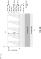
- Fig. 6A-6G are diagrams of an example implementation 600 relating to example process 400 shown in Fig. 4 . As shown, Figs. 6A-6G illustrate examples of etching a set of layers and removing a set of masks from the set of layers as described, above, with regard to blocks 430 and 440.
- example implementation 600 from reference line 602 to reference line 610 may include a set of layers 612 to 632.
- the set of layers 612 to 632 may be planar and unetched.
- example implementation 600 may include a substrate layer 614.
- An anti-reflectance layer 612 may be deposited onto a first side of substrate layer 614 and a set of alternating silicon layers 616, 620, 624, 628, and 632 and silicon dioxide layers 618, 622, 626, and 630 may be deposited onto a second side of substrate layer 614.
- mask layers 634, 636, and 638 are deposited and patterned to cover portions of silicon layer 632 to enabling an etching procedure and a mask removal procedure to be performed to form a set of four anti-reflectance structures between reference lines 602 and 610.
- the materials used for each mask 634, 636, 638 may be dissimilar so that the removal of one does not affect the pattern of the remaining mask(s).
- a first etch step of an etching procedure may be performed to remove a portion of silicon layer 632, silicon dioxide layer 630, and silicon layer 628 not covered by mask layer 638 (e.g., between reference lines 602 and 604).
- silicon dioxide layer 626 may perform an etch stop functionality for the first etching step.
- a first mask removal step of a mask removal procedure may be performed to remove mask layer 638, thereby exposing a portion of silicon layer 632 between reference lines 604 and 606 and a portion of mask layer 636 between reference lines 606 and 610.
- a second etch step of the etching procedure may be performed to remove silicon dioxide layer 626 and silicon layer 624 between reference lines 602 and 604, and to remove silicon layer 632, silicon dioxide layer 630, and silicon layer 628 between reference lines 604 and 606.
- silicon dioxide layer 622 may perform an etch stop functionality for the second etch step between reference lines 602 and 604
- silicon dioxide layer 626 may perform an etch stop functionality for the second etch step between reference lines 604 and 606.
- a second mask removal step of the mask removal procedure may be performed to remove mask layer 636, thereby exposing silicon layer 632 between reference lines 606 and 608 and a portion of mask layer 634 between reference lines 608 and 610.
- a third etch step of the etching procedure may be performed to remove silicon dioxide layer 622 and silicon layer 620 between reference lines 602 and 604; silicon dioxide layer 626 and silicon layer 624 between reference lines 604 and 606; and silicon layer 632, silicon dioxide layer 630, and silicon layer 628 between reference lines 606 and 608.
- silicon dioxide layer 618 may perform an etch stop functionality for the third etch step between reference lines 602 and 604
- silicon dioxide layer 622 may perform an etch stop functionality for the third etch step between reference lines 604 and 606
- silicon dioxide layer 626 may perform an etch stop functionality for the third etch step between reference lines 606 and 608.
- a third mask removal step of the mask removal procedure may be performed to remove mask layer 634, thereby exposing silicon layer 632 between reference lines 608 and 610.
- a 4-level relief profile may be formed with a first anti-reflectance structure for a particular wavelength between reference lines 602 and 604, a second anti-reflectance structure for the particular wavelength between reference lines 604 and 606, a third anti-reflectance structure for the particular wavelength between reference lines 606 and 608, and a fourth anti-reflectance structure and another silicon layer (e.g., silicon layer 628) between reference lines 608 and 610.
- a phase delay between the first anti-reflectance structure between reference lines 602 and 604 and the fourth anti-reflectance structure between reference lines 608 and 610 may be a ⁇ phase delay.
- FIGS. 6A-6G are provided merely as an example. Other examples are possible and may differ from what was described with regard to Figs. 6A-6G .
- a DOE with a thin film stack including alternating silicon layers (e.g., hydrogenated silicon layers) and silicon dioxide layers etched into a multi-level (e.g., three or more level) relief profile is configured and manufactured.
- layers of the DOE may be designed to provide anti-reflectance properties, integrated etch stop properties, and/or the like.
- design may be performed using thin film process deposition, which may control zero order power.
- a quantity of manufacture steps to manufacture the DOE may be reduced, thereby reducing time and cost relative to other techniques for manufacturing a DOE.
- the relief depths and anti-reflection structures have been illustrated as a periodic or repeating pattern and with a constant cross-section, such as found in a diffraction grating.
- Other, non-periodic relief depths and anti-reflection structures with irregular or variable cross-sections are equally contemplated, such as, but not limited to, DOEs for pattern generation, depth mapping dot projection, and structured light.
- satisfying a threshold may refer to a value being greater than the threshold, more than the threshold, higher than the threshold, greater than or equal to the threshold, less than the threshold, fewer than the threshold, lower than the threshold, less than or equal to the threshold, equal to the threshold, or the like.
Landscapes
- Physics & Mathematics (AREA)
- General Physics & Mathematics (AREA)
- Optics & Photonics (AREA)
- Engineering & Computer Science (AREA)
- Manufacturing & Machinery (AREA)
- Chemical & Material Sciences (AREA)
- Inorganic Chemistry (AREA)
- Diffracting Gratings Or Hologram Optical Elements (AREA)
- Surface Treatment Of Optical Elements (AREA)
- Optical Integrated Circuits (AREA)
Applications Claiming Priority (2)
| Application Number | Priority Date | Filing Date | Title |
|---|---|---|---|
| US201762546172P | 2017-08-16 | 2017-08-16 | |
| US16/044,081 US10802185B2 (en) | 2017-08-16 | 2018-07-24 | Multi-level diffractive optical element thin film coating |
Publications (2)
| Publication Number | Publication Date |
|---|---|
| EP3444643A1 EP3444643A1 (en) | 2019-02-20 |
| EP3444643B1 true EP3444643B1 (en) | 2024-10-09 |
Family
ID=63209272
Family Applications (1)
| Application Number | Title | Priority Date | Filing Date |
|---|---|---|---|
| EP18188469.3A Active EP3444643B1 (en) | 2017-08-16 | 2018-08-10 | Multi-level diffractive optical element thin film coating |
Country Status (7)
Families Citing this family (8)
| Publication number | Priority date | Publication date | Assignee | Title |
|---|---|---|---|---|
| US10712475B2 (en) | 2017-08-16 | 2020-07-14 | Lumentum Operations Llc | Multi-layer thin film stack for diffractive optical elements |
| US10802185B2 (en) | 2017-08-16 | 2020-10-13 | Lumentum Operations Llc | Multi-level diffractive optical element thin film coating |
| US11187836B2 (en) * | 2018-03-06 | 2021-11-30 | Applied Materials, Inc. | Method of building a 3D functional optical material layer stacking structure |
| KR102357157B1 (ko) * | 2019-04-16 | 2022-01-28 | 한국과학기술원 | 음향 광학 상호 작용 구조체 |
| US11347087B2 (en) | 2019-04-16 | 2022-05-31 | Korea Advanced Institute Of Science And Technology | Acousto-optic interactive structure |
| US11892619B2 (en) * | 2019-09-04 | 2024-02-06 | Lumentum Operations Llc | MEMS device with a three-layer comb actuator structure and a two-layer hinge |
| US11782195B2 (en) | 2019-09-30 | 2023-10-10 | Himax Technologies Limited | Diffractive optical element and method for fabricating the diffractive optical element |
| WO2021224450A1 (en) * | 2020-05-08 | 2021-11-11 | Nil Technology Aps | Multi-level structures and methods for manufacturing the same |
Citations (1)
| Publication number | Priority date | Publication date | Assignee | Title |
|---|---|---|---|---|
| US20180143359A1 (en) * | 2016-11-21 | 2018-05-24 | Stmicroelectronics (Research & Development) Limited | Wafer level microstructures for an optical lens |
Family Cites Families (40)
| Publication number | Priority date | Publication date | Assignee | Title |
|---|---|---|---|---|
| US5161059A (en) | 1987-09-21 | 1992-11-03 | Massachusetts Institute Of Technology | High-efficiency, multilevel, diffractive optical elements |
| US4895790A (en) | 1987-09-21 | 1990-01-23 | Massachusetts Institute Of Technology | High-efficiency, multilevel, diffractive optical elements |
| US5245468A (en) | 1990-12-14 | 1993-09-14 | Ford Motor Company | Anti-reflective transparent coating |
| JPH0643311A (ja) * | 1992-07-22 | 1994-02-18 | Nippon Telegr & Teleph Corp <Ntt> | 回折光学素子及びその製造方法 |
| US5446587A (en) * | 1992-09-03 | 1995-08-29 | Samsung Electronics Co., Ltd. | Projection method and projection system and mask therefor |
| US5606434A (en) | 1994-06-30 | 1997-02-25 | University Of North Carolina | Achromatic optical system including diffractive optical element |
| US6829091B2 (en) | 1997-02-07 | 2004-12-07 | Canon Kabushiki Kaisha | Optical system and optical instrument with diffractive optical element |
| US6055262A (en) | 1997-06-11 | 2000-04-25 | Honeywell Inc. | Resonant reflector for improved optoelectronic device performance and enhanced applicability |
| JPH11174217A (ja) * | 1997-12-16 | 1999-07-02 | Canon Inc | 回折光学素子及びその製造方法 |
| JP2000098116A (ja) * | 1998-09-18 | 2000-04-07 | Canon Inc | 素子又は素子作製用モールド型の作製方法 |
| JP3442004B2 (ja) * | 1999-07-30 | 2003-09-02 | キヤノン株式会社 | 光学素子の製造方法 |
| JP3381150B2 (ja) | 1999-08-30 | 2003-02-24 | スタンレー電気株式会社 | 赤外線透過フィルタ及びその製造方法 |
| JP2004028862A (ja) | 2002-06-27 | 2004-01-29 | Harmonic Drive Syst Ind Co Ltd | 投影型エンコーダ |
| US6905618B2 (en) * | 2002-07-30 | 2005-06-14 | Agilent Technologies, Inc. | Diffractive optical elements and methods of making the same |
| EP1602947A4 (en) | 2003-03-13 | 2007-03-28 | Asahi Glass Co Ltd | Diffraction element and optical device |
| US20040263981A1 (en) * | 2003-06-27 | 2004-12-30 | Coleman Christopher L. | Diffractive optical element with anti-reflection coating |
| FR2861183B1 (fr) | 2003-10-15 | 2006-01-21 | Thales Sa | Elements d'optique diffractive de type binaire pour une utilisation sur une large bande spectrale |
| DE102005020944A1 (de) | 2004-05-04 | 2005-12-01 | Friedrich-Schiller-Universität Jena | Diffraktive Elemente mit Antireflex-Eigenschaften |
| US7879209B2 (en) | 2004-08-20 | 2011-02-01 | Jds Uniphase Corporation | Cathode for sputter coating |
| KR100641006B1 (ko) * | 2004-11-04 | 2006-11-02 | 엘지.필립스 엘시디 주식회사 | 인쇄판 |
| JP2007234094A (ja) | 2006-02-28 | 2007-09-13 | Epson Toyocom Corp | 回折格子体、これを用いた光ヘッド装置及び回折格子体の製造方法 |
| EP1855127A1 (en) | 2006-05-12 | 2007-11-14 | Rolic AG | Optically effective surface relief microstructures and method of making them |
| CA2600900A1 (en) * | 2006-09-21 | 2008-03-21 | Nippon Sheet Glass Company, Limited | Transmissive diffraction grating, and spectral separation element and spectroscope using the same |
| JP5280654B2 (ja) | 2006-09-21 | 2013-09-04 | 日本板硝子株式会社 | 透過型回折格子、並びに、それを用いた分光素子及び分光器 |
| CN101140400A (zh) | 2007-10-19 | 2008-03-12 | 中国科学院上海光学精密机械研究所 | 脉冲压缩光栅用多层介质膜的优化设计方法 |
| US8384997B2 (en) | 2008-01-21 | 2013-02-26 | Primesense Ltd | Optical pattern projection |
| TWI409852B (zh) | 2009-12-31 | 2013-09-21 | Inotera Memories Inc | 利用自對準雙重圖案製作半導體元件微細結構的方法 |
| JP2011187139A (ja) * | 2010-03-10 | 2011-09-22 | Hitachi Maxell Ltd | グレーティング素子及びその製造方法、並びに、そのグレーティング素子を用いた光ピックアップ装置 |
| JP2012039042A (ja) * | 2010-08-11 | 2012-02-23 | Sony Corp | メモリ素子 |
| FR2981460B1 (fr) * | 2011-10-18 | 2016-06-24 | Commissariat Energie Atomique | Procede de realisation d'un dispositif optique refractif ou diffractif |
| TWI684031B (zh) | 2012-07-16 | 2020-02-01 | 美商唯亞威方案公司 | 光學濾波器及感測器系統 |
| CN103424995B (zh) | 2013-06-05 | 2015-02-11 | 上海理工大学 | 导模共振滤光片光刻胶层的优化方法 |
| DE102015218702A1 (de) | 2015-09-29 | 2017-03-30 | Dr. Johannes Heidenhain Gmbh | Optisches Schichtsystem |
| US9960199B2 (en) | 2015-12-29 | 2018-05-01 | Viavi Solutions Inc. | Dielectric mirror based multispectral filter array |
| FR3047810B1 (fr) | 2016-02-12 | 2018-05-25 | Thales | Composant diffractif sub longueur d'onde large bande spectracle |
| CN106654858B (zh) | 2017-03-08 | 2021-03-19 | 长春理工大学 | 具有双层亚波长光栅反射镜的垂直腔面发射半导体激光器 |
| JP6981074B2 (ja) * | 2017-07-25 | 2021-12-15 | Agc株式会社 | 光学素子 |
| DE102017213330A1 (de) | 2017-08-02 | 2019-02-07 | Dr. Johannes Heidenhain Gmbh | Abtastplatte für eine optische Positionsmesseinrichtung |
| US10712475B2 (en) | 2017-08-16 | 2020-07-14 | Lumentum Operations Llc | Multi-layer thin film stack for diffractive optical elements |
| US10802185B2 (en) | 2017-08-16 | 2020-10-13 | Lumentum Operations Llc | Multi-level diffractive optical element thin film coating |
-
2018
- 2018-07-24 US US16/044,081 patent/US10802185B2/en active Active
- 2018-08-02 JP JP2018146142A patent/JP7330675B2/ja active Active
- 2018-08-03 TW TW111102948A patent/TWI809675B/zh active
- 2018-08-03 TW TW107127006A patent/TWI756459B/zh active
- 2018-08-09 IL IL261086A patent/IL261086B2/en unknown
- 2018-08-10 EP EP18188469.3A patent/EP3444643B1/en active Active
- 2018-08-16 KR KR1020180095665A patent/KR102421825B1/ko active Active
- 2018-08-16 CN CN201810934058.1A patent/CN109407191A/zh active Pending
-
2020
- 2020-09-30 US US16/948,732 patent/US11686890B2/en active Active
-
2022
- 2022-05-31 JP JP2022089078A patent/JP7348991B2/ja active Active
Patent Citations (1)
| Publication number | Priority date | Publication date | Assignee | Title |
|---|---|---|---|---|
| US20180143359A1 (en) * | 2016-11-21 | 2018-05-24 | Stmicroelectronics (Research & Development) Limited | Wafer level microstructures for an optical lens |
Also Published As
| Publication number | Publication date |
|---|---|
| CN109407191A (zh) | 2019-03-01 |
| US20210026051A1 (en) | 2021-01-28 |
| US11686890B2 (en) | 2023-06-27 |
| US20190056542A1 (en) | 2019-02-21 |
| IL261086A (en) | 2019-01-31 |
| IL261086B2 (en) | 2023-06-01 |
| JP2022130387A (ja) | 2022-09-06 |
| KR20190019029A (ko) | 2019-02-26 |
| TWI809675B (zh) | 2023-07-21 |
| KR102421825B1 (ko) | 2022-07-15 |
| JP7348991B2 (ja) | 2023-09-21 |
| TW201910915A (zh) | 2019-03-16 |
| TWI756459B (zh) | 2022-03-01 |
| TW202219629A (zh) | 2022-05-16 |
| JP2019035954A (ja) | 2019-03-07 |
| JP7330675B2 (ja) | 2023-08-22 |
| EP3444643A1 (en) | 2019-02-20 |
| US10802185B2 (en) | 2020-10-13 |
Similar Documents
| Publication | Publication Date | Title |
|---|---|---|
| EP3444643B1 (en) | Multi-level diffractive optical element thin film coating | |
| US11543562B2 (en) | Multi-layer thin film stack for diffractive optical elements | |
| US11762134B2 (en) | Diffractive optical element | |
| EP2943823B1 (en) | Diffraction gratings and the manufacture thereof | |
| JP7678028B2 (ja) | 角度付き格子の形成 | |
| CN100526918C (zh) | 衍射光栅元件 | |
| KR102096682B1 (ko) | 광파면의 위상을 제어하기 위한 디바이스 | |
| JP2005084485A (ja) | 回折光学素子 | |
| US20240192431A1 (en) | Thin film layers having non-uniform thicknesses |
Legal Events
| Date | Code | Title | Description |
|---|---|---|---|
| PUAI | Public reference made under article 153(3) epc to a published international application that has entered the european phase |
Free format text: ORIGINAL CODE: 0009012 |
|
| STAA | Information on the status of an ep patent application or granted ep patent |
Free format text: STATUS: THE APPLICATION HAS BEEN PUBLISHED |
|
| AK | Designated contracting states |
Kind code of ref document: A1 Designated state(s): AL AT BE BG CH CY CZ DE DK EE ES FI FR GB GR HR HU IE IS IT LI LT LU LV MC MK MT NL NO PL PT RO RS SE SI SK SM TR |
|
| AX | Request for extension of the european patent |
Extension state: BA ME |
|
| STAA | Information on the status of an ep patent application or granted ep patent |
Free format text: STATUS: REQUEST FOR EXAMINATION WAS MADE |
|
| 17P | Request for examination filed |
Effective date: 20190814 |
|
| RBV | Designated contracting states (corrected) |
Designated state(s): AL AT BE BG CH CY CZ DE DK EE ES FI FR GB GR HR HU IE IS IT LI LT LU LV MC MK MT NL NO PL PT RO RS SE SI SK SM TR |
|
| STAA | Information on the status of an ep patent application or granted ep patent |
Free format text: STATUS: EXAMINATION IS IN PROGRESS |
|
| 17Q | First examination report despatched |
Effective date: 20210423 |
|
| STAA | Information on the status of an ep patent application or granted ep patent |
Free format text: STATUS: EXAMINATION IS IN PROGRESS |
|
| GRAP | Despatch of communication of intention to grant a patent |
Free format text: ORIGINAL CODE: EPIDOSNIGR1 |
|
| STAA | Information on the status of an ep patent application or granted ep patent |
Free format text: STATUS: GRANT OF PATENT IS INTENDED |
|
| RIC1 | Information provided on ipc code assigned before grant |
Ipc: G02B 27/42 20060101ALN20231113BHEP Ipc: G02B 27/10 20060101ALN20231113BHEP Ipc: G02B 27/44 20060101ALI20231113BHEP Ipc: G02B 5/18 20060101ALI20231113BHEP Ipc: G02B 1/115 20150101AFI20231113BHEP |
|
| INTG | Intention to grant announced |
Effective date: 20231215 |
|
| GRAJ | Information related to disapproval of communication of intention to grant by the applicant or resumption of examination proceedings by the epo deleted |
Free format text: ORIGINAL CODE: EPIDOSDIGR1 |
|
| STAA | Information on the status of an ep patent application or granted ep patent |
Free format text: STATUS: EXAMINATION IS IN PROGRESS |
|
| GRAP | Despatch of communication of intention to grant a patent |
Free format text: ORIGINAL CODE: EPIDOSNIGR1 |
|
| STAA | Information on the status of an ep patent application or granted ep patent |
Free format text: STATUS: GRANT OF PATENT IS INTENDED |
|
| INTC | Intention to grant announced (deleted) | ||
| RIC1 | Information provided on ipc code assigned before grant |
Ipc: G02B 27/42 20060101ALN20240416BHEP Ipc: G02B 27/10 20060101ALN20240416BHEP Ipc: G02B 27/44 20060101ALI20240416BHEP Ipc: G02B 5/18 20060101ALI20240416BHEP Ipc: G02B 1/115 20150101AFI20240416BHEP |
|
| INTG | Intention to grant announced |
Effective date: 20240502 |
|
| RIC1 | Information provided on ipc code assigned before grant |
Ipc: G02B 27/42 20060101ALN20240422BHEP Ipc: G02B 27/10 20060101ALN20240422BHEP Ipc: G02B 27/44 20060101ALI20240422BHEP Ipc: G02B 5/18 20060101ALI20240422BHEP Ipc: G02B 1/115 20150101AFI20240422BHEP |
|
| GRAS | Grant fee paid |
Free format text: ORIGINAL CODE: EPIDOSNIGR3 |
|
| GRAA | (expected) grant |
Free format text: ORIGINAL CODE: 0009210 |
|
| STAA | Information on the status of an ep patent application or granted ep patent |
Free format text: STATUS: THE PATENT HAS BEEN GRANTED |
|
| AK | Designated contracting states |
Kind code of ref document: B1 Designated state(s): AL AT BE BG CH CY CZ DE DK EE ES FI FR GB GR HR HU IE IS IT LI LT LU LV MC MK MT NL NO PL PT RO RS SE SI SK SM TR |
|
| REG | Reference to a national code |
Ref country code: CH Ref legal event code: EP |
|
| REG | Reference to a national code |
Ref country code: DE Ref legal event code: R096 Ref document number: 602018075127 Country of ref document: DE |
|
| REG | Reference to a national code |
Ref country code: IE Ref legal event code: FG4D |
|
| REG | Reference to a national code |
Ref country code: LT Ref legal event code: MG9D |
|
| REG | Reference to a national code |
Ref country code: NL Ref legal event code: MP Effective date: 20241009 |
|
| REG | Reference to a national code |
Ref country code: AT Ref legal event code: MK05 Ref document number: 1731159 Country of ref document: AT Kind code of ref document: T Effective date: 20241009 |
|
| PG25 | Lapsed in a contracting state [announced via postgrant information from national office to epo] |
Ref country code: NL Free format text: LAPSE BECAUSE OF FAILURE TO SUBMIT A TRANSLATION OF THE DESCRIPTION OR TO PAY THE FEE WITHIN THE PRESCRIBED TIME-LIMIT Effective date: 20241009 |
|
| PG25 | Lapsed in a contracting state [announced via postgrant information from national office to epo] |
Ref country code: NL Free format text: LAPSE BECAUSE OF FAILURE TO SUBMIT A TRANSLATION OF THE DESCRIPTION OR TO PAY THE FEE WITHIN THE PRESCRIBED TIME-LIMIT Effective date: 20241009 |
|
| PG25 | Lapsed in a contracting state [announced via postgrant information from national office to epo] |
Ref country code: PT Free format text: LAPSE BECAUSE OF FAILURE TO SUBMIT A TRANSLATION OF THE DESCRIPTION OR TO PAY THE FEE WITHIN THE PRESCRIBED TIME-LIMIT Effective date: 20250210 Ref country code: HR Free format text: LAPSE BECAUSE OF FAILURE TO SUBMIT A TRANSLATION OF THE DESCRIPTION OR TO PAY THE FEE WITHIN THE PRESCRIBED TIME-LIMIT Effective date: 20241009 Ref country code: IS Free format text: LAPSE BECAUSE OF FAILURE TO SUBMIT A TRANSLATION OF THE DESCRIPTION OR TO PAY THE FEE WITHIN THE PRESCRIBED TIME-LIMIT Effective date: 20250209 |
|
| PG25 | Lapsed in a contracting state [announced via postgrant information from national office to epo] |
Ref country code: FI Free format text: LAPSE BECAUSE OF FAILURE TO SUBMIT A TRANSLATION OF THE DESCRIPTION OR TO PAY THE FEE WITHIN THE PRESCRIBED TIME-LIMIT Effective date: 20241009 |
|
| PG25 | Lapsed in a contracting state [announced via postgrant information from national office to epo] |
Ref country code: BG Free format text: LAPSE BECAUSE OF FAILURE TO SUBMIT A TRANSLATION OF THE DESCRIPTION OR TO PAY THE FEE WITHIN THE PRESCRIBED TIME-LIMIT Effective date: 20241009 |
|
| PG25 | Lapsed in a contracting state [announced via postgrant information from national office to epo] |
Ref country code: ES Free format text: LAPSE BECAUSE OF FAILURE TO SUBMIT A TRANSLATION OF THE DESCRIPTION OR TO PAY THE FEE WITHIN THE PRESCRIBED TIME-LIMIT Effective date: 20241009 |
|
| PG25 | Lapsed in a contracting state [announced via postgrant information from national office to epo] |
Ref country code: NO Free format text: LAPSE BECAUSE OF FAILURE TO SUBMIT A TRANSLATION OF THE DESCRIPTION OR TO PAY THE FEE WITHIN THE PRESCRIBED TIME-LIMIT Effective date: 20250109 |
|
| PG25 | Lapsed in a contracting state [announced via postgrant information from national office to epo] |
Ref country code: GR Free format text: LAPSE BECAUSE OF FAILURE TO SUBMIT A TRANSLATION OF THE DESCRIPTION OR TO PAY THE FEE WITHIN THE PRESCRIBED TIME-LIMIT Effective date: 20250110 Ref country code: LV Free format text: LAPSE BECAUSE OF FAILURE TO SUBMIT A TRANSLATION OF THE DESCRIPTION OR TO PAY THE FEE WITHIN THE PRESCRIBED TIME-LIMIT Effective date: 20241009 Ref country code: AT Free format text: LAPSE BECAUSE OF FAILURE TO SUBMIT A TRANSLATION OF THE DESCRIPTION OR TO PAY THE FEE WITHIN THE PRESCRIBED TIME-LIMIT Effective date: 20241009 |
|
| PG25 | Lapsed in a contracting state [announced via postgrant information from national office to epo] |
Ref country code: PL Free format text: LAPSE BECAUSE OF FAILURE TO SUBMIT A TRANSLATION OF THE DESCRIPTION OR TO PAY THE FEE WITHIN THE PRESCRIBED TIME-LIMIT Effective date: 20241009 |
|
| PG25 | Lapsed in a contracting state [announced via postgrant information from national office to epo] |
Ref country code: RS Free format text: LAPSE BECAUSE OF FAILURE TO SUBMIT A TRANSLATION OF THE DESCRIPTION OR TO PAY THE FEE WITHIN THE PRESCRIBED TIME-LIMIT Effective date: 20250109 |
|
| PG25 | Lapsed in a contracting state [announced via postgrant information from national office to epo] |
Ref country code: SM Free format text: LAPSE BECAUSE OF FAILURE TO SUBMIT A TRANSLATION OF THE DESCRIPTION OR TO PAY THE FEE WITHIN THE PRESCRIBED TIME-LIMIT Effective date: 20241009 |
|
| PG25 | Lapsed in a contracting state [announced via postgrant information from national office to epo] |
Ref country code: DK Free format text: LAPSE BECAUSE OF FAILURE TO SUBMIT A TRANSLATION OF THE DESCRIPTION OR TO PAY THE FEE WITHIN THE PRESCRIBED TIME-LIMIT Effective date: 20241009 |
|
| REG | Reference to a national code |
Ref country code: DE Ref legal event code: R097 Ref document number: 602018075127 Country of ref document: DE |
|
| PG25 | Lapsed in a contracting state [announced via postgrant information from national office to epo] |
Ref country code: EE Free format text: LAPSE BECAUSE OF FAILURE TO SUBMIT A TRANSLATION OF THE DESCRIPTION OR TO PAY THE FEE WITHIN THE PRESCRIBED TIME-LIMIT Effective date: 20241009 |
|
| PG25 | Lapsed in a contracting state [announced via postgrant information from national office to epo] |
Ref country code: RO Free format text: LAPSE BECAUSE OF FAILURE TO SUBMIT A TRANSLATION OF THE DESCRIPTION OR TO PAY THE FEE WITHIN THE PRESCRIBED TIME-LIMIT Effective date: 20241009 |
|
| PG25 | Lapsed in a contracting state [announced via postgrant information from national office to epo] |
Ref country code: SK Free format text: LAPSE BECAUSE OF FAILURE TO SUBMIT A TRANSLATION OF THE DESCRIPTION OR TO PAY THE FEE WITHIN THE PRESCRIBED TIME-LIMIT Effective date: 20241009 |
|
| PG25 | Lapsed in a contracting state [announced via postgrant information from national office to epo] |
Ref country code: CZ Free format text: LAPSE BECAUSE OF FAILURE TO SUBMIT A TRANSLATION OF THE DESCRIPTION OR TO PAY THE FEE WITHIN THE PRESCRIBED TIME-LIMIT Effective date: 20241009 |
|
| PG25 | Lapsed in a contracting state [announced via postgrant information from national office to epo] |
Ref country code: IT Free format text: LAPSE BECAUSE OF FAILURE TO SUBMIT A TRANSLATION OF THE DESCRIPTION OR TO PAY THE FEE WITHIN THE PRESCRIBED TIME-LIMIT Effective date: 20241009 |
|
| PLBE | No opposition filed within time limit |
Free format text: ORIGINAL CODE: 0009261 |
|
| STAA | Information on the status of an ep patent application or granted ep patent |
Free format text: STATUS: NO OPPOSITION FILED WITHIN TIME LIMIT |