EP3432221A1 - Carte électronique comprenant un capteur d'empreinte et procédé de fabrication d'une telle carte - Google Patents
Carte électronique comprenant un capteur d'empreinte et procédé de fabrication d'une telle carte Download PDFInfo
- Publication number
- EP3432221A1 EP3432221A1 EP18305953.4A EP18305953A EP3432221A1 EP 3432221 A1 EP3432221 A1 EP 3432221A1 EP 18305953 A EP18305953 A EP 18305953A EP 3432221 A1 EP3432221 A1 EP 3432221A1
- Authority
- EP
- European Patent Office
- Prior art keywords
- module
- cavity
- card
- card body
- electronic card
- Prior art date
- Legal status (The legal status is an assumption and is not a legal conclusion. Google has not performed a legal analysis and makes no representation as to the accuracy of the status listed.)
- Granted
Links
Images


Classifications
-
- G—PHYSICS
- G06—COMPUTING OR CALCULATING; COUNTING
- G06V—IMAGE OR VIDEO RECOGNITION OR UNDERSTANDING
- G06V40/00—Recognition of biometric, human-related or animal-related patterns in image or video data
- G06V40/10—Human or animal bodies, e.g. vehicle occupants or pedestrians; Body parts, e.g. hands
- G06V40/12—Fingerprints or palmprints
- G06V40/13—Sensors therefor
- G06V40/1306—Sensors therefor non-optical, e.g. ultrasonic or capacitive sensing
-
- G—PHYSICS
- G06—COMPUTING OR CALCULATING; COUNTING
- G06K—GRAPHICAL DATA READING; PRESENTATION OF DATA; RECORD CARRIERS; HANDLING RECORD CARRIERS
- G06K19/00—Record carriers for use with machines and with at least a part designed to carry digital markings
- G06K19/06—Record carriers for use with machines and with at least a part designed to carry digital markings characterised by the kind of the digital marking, e.g. shape, nature, code
- G06K19/067—Record carriers with conductive marks, printed circuits or semiconductor circuit elements, e.g. credit or identity cards also with resonating or responding marks without active components
- G06K19/07—Record carriers with conductive marks, printed circuits or semiconductor circuit elements, e.g. credit or identity cards also with resonating or responding marks without active components with integrated circuit chips
- G06K19/0716—Record carriers with conductive marks, printed circuits or semiconductor circuit elements, e.g. credit or identity cards also with resonating or responding marks without active components with integrated circuit chips at least one of the integrated circuit chips comprising a sensor or an interface to a sensor
- G06K19/0718—Record carriers with conductive marks, printed circuits or semiconductor circuit elements, e.g. credit or identity cards also with resonating or responding marks without active components with integrated circuit chips at least one of the integrated circuit chips comprising a sensor or an interface to a sensor the sensor being of the biometric kind, e.g. fingerprint sensors
-
- G—PHYSICS
- G06—COMPUTING OR CALCULATING; COUNTING
- G06K—GRAPHICAL DATA READING; PRESENTATION OF DATA; RECORD CARRIERS; HANDLING RECORD CARRIERS
- G06K19/00—Record carriers for use with machines and with at least a part designed to carry digital markings
- G06K19/06—Record carriers for use with machines and with at least a part designed to carry digital markings characterised by the kind of the digital marking, e.g. shape, nature, code
- G06K19/067—Record carriers with conductive marks, printed circuits or semiconductor circuit elements, e.g. credit or identity cards also with resonating or responding marks without active components
- G06K19/07—Record carriers with conductive marks, printed circuits or semiconductor circuit elements, e.g. credit or identity cards also with resonating or responding marks without active components with integrated circuit chips
- G06K19/077—Constructional details, e.g. mounting of circuits in the carrier
- G06K19/07701—Constructional details, e.g. mounting of circuits in the carrier the record carrier comprising an interface suitable for human interaction
-
- G—PHYSICS
- G06—COMPUTING OR CALCULATING; COUNTING
- G06K—GRAPHICAL DATA READING; PRESENTATION OF DATA; RECORD CARRIERS; HANDLING RECORD CARRIERS
- G06K19/00—Record carriers for use with machines and with at least a part designed to carry digital markings
- G06K19/06—Record carriers for use with machines and with at least a part designed to carry digital markings characterised by the kind of the digital marking, e.g. shape, nature, code
- G06K19/067—Record carriers with conductive marks, printed circuits or semiconductor circuit elements, e.g. credit or identity cards also with resonating or responding marks without active components
- G06K19/07—Record carriers with conductive marks, printed circuits or semiconductor circuit elements, e.g. credit or identity cards also with resonating or responding marks without active components with integrated circuit chips
- G06K19/077—Constructional details, e.g. mounting of circuits in the carrier
- G06K19/07745—Mounting details of integrated circuit chips
- G06K19/07747—Mounting details of integrated circuit chips at least one of the integrated circuit chips being mounted as a module
-
- G—PHYSICS
- G06—COMPUTING OR CALCULATING; COUNTING
- G06K—GRAPHICAL DATA READING; PRESENTATION OF DATA; RECORD CARRIERS; HANDLING RECORD CARRIERS
- G06K19/00—Record carriers for use with machines and with at least a part designed to carry digital markings
- G06K19/06—Record carriers for use with machines and with at least a part designed to carry digital markings characterised by the kind of the digital marking, e.g. shape, nature, code
- G06K19/08—Record carriers for use with machines and with at least a part designed to carry digital markings characterised by the kind of the digital marking, e.g. shape, nature, code using markings of different kinds or more than one marking of the same kind in the same record carrier, e.g. one marking being sensed by optical and the other by magnetic means
- G06K19/10—Record carriers for use with machines and with at least a part designed to carry digital markings characterised by the kind of the digital marking, e.g. shape, nature, code using markings of different kinds or more than one marking of the same kind in the same record carrier, e.g. one marking being sensed by optical and the other by magnetic means at least one kind of marking being used for authentication, e.g. of credit or identity cards
- G06K19/18—Constructional details
-
- G—PHYSICS
- G06—COMPUTING OR CALCULATING; COUNTING
- G06V—IMAGE OR VIDEO RECOGNITION OR UNDERSTANDING
- G06V40/00—Recognition of biometric, human-related or animal-related patterns in image or video data
- G06V40/10—Human or animal bodies, e.g. vehicle occupants or pedestrians; Body parts, e.g. hands
- G06V40/12—Fingerprints or palmprints
- G06V40/13—Sensors therefor
- G06V40/1329—Protecting the fingerprint sensor against damage caused by the finger
Definitions
- the invention relates to the field of electronic cards and the manufacture of such cards and relates more particularly to electronic cards comprising a fingerprint sensor.
- a problem is that the fingerprint sensors are fragile and may not necessarily support such flexibility and size requirements.
- the imprint sensor requires that some of its components (typically the processor and / or the memory) are mounted within a recessed layer (inlay in English) between the two plastic layers of the map.
- An object of the invention is to have an electronic card comprising a fingerprint sensor that satisfies the constraints specified in the standard standards.
- ISO 781 ID1 ISO 7816 for banking applications
- ISO 10373 in terms of size and flexibility.
- Another object of the invention is to have a method of manufacturing an electronic card comprising a fingerprint sensor that is simple to implement.
- a fingerprint module flush with the upper surface of the card body has advantages of ergonomics, ease of manufacture, strength and durability of the card it equips with respect to a fingerprint module that would be protruding or conversely in a recess with respect to the upper surface of the card body.
- a fingerprint module that protrudes from the upper surface would introduce difficulties or impossibility of introduction of the card in terminals, for example in ATMs.
- a module of fingerprints that would be in a recess relative to the upper surface would weaken the structure of the card and complicate the large-scale manufacture.
- the life of the card would also be reduced by the accumulation of impurities and dust in the gap between the upper surface and the fingerprint module, which would eventually damage the device.
- a fingerprint module flush with the upper surface of the card optimizes the comfort of a user positioning his finger on the fingerprint module, the user does not feel a protrusion or a recess under his finger when he positions it.
- the invention is advantageously completed by the following characteristics, taken alone or in any of their technically possible combination.
- the fingerprint module further comprises connection pads for connecting said fingerprint module to an antenna or a second module.
- the cavity has a maximum depth such that the distance between the bottom surface of the card body and the bottom of the cavity is greater than or equal to 160 ⁇ m.
- the cavity has a three-dimensional internal profile so as to follow the internal relief of the cavity module, the cavity comprising at least one stop configured to limit the deformations of the module housed in the cavity.
- the card includes two cavities, a cavity housing the cavity module, the other cavity housing a second module typically bank or access.
- the card body comprises an intermediate layer, called interconnection layer, of conductive material on which an antenna is integrated.
- the card body comprises an intermediate layer, called interconnection layer, of semiconductor material on which a circuit configured to connect the imprint module to the second module.
- the card includes recesses formed from the at least one cavity to the interconnect layer.
- the card further comprises a tactile mark and / or an alignment mark disposed on the upper surface of the card body near the fingerprint module, said touch mark being configured to allow correct positioning of a finger on the fingerprint module.
- the step of obtaining the card body comprises a substep of integration of an antenna on the intermediate layer.
- the method further comprises obtaining two cavities in the card body, and placing the impression module in one of the two cavities and placing a second module in the other cavity, the step of obtaining the card body further comprises a step of integrating a connection circuit configured to connect the fingerprint module to the second module.
- the step of obtaining the card body comprises a substep of hot lamination of the upper layer, the first substrate, the intermediate layer and the lower layer.
- the method comprises a step of obtaining at least one recess in the card body from the cavity to the intermediate layer.
- the entire cavity module is housed in the same cavity. There is therefore no need to provide additional connection or cavity to accommodate this module.
- the fingerprint module can easily integrate into a conventional electronic card.
- the Figures 1a and 1b illustrate an electronic card comprising a card body 1 and a fingerprint module 2.
- the card body 1 comprises an upper surface 11 and a lower surface 12 and has dimensions compliant with the ISO 781 ID1 standard.
- the card body 1 has a thickness of between 780 and 840 ⁇ m.
- the card body comprises several layers assembled together by means of a hot lamination process so as to satisfy the constraints of resistance of the layers to each other of the ISO 781 ID1 standard.
- the electronic card comprises an imprint module 2 housed in a cavity 13 formed in the thickness of the card body 1.
- the cavity 13 opens out of the upper surface 11 of the card body 1 and is flush with the upper surface of the card body.
- the cavity 13 is advantageously obtained by milling the card body 1 to a desired thickness.
- the imprint module 2 is configured to acquire the image of a fingerprint of a user and to verify the identity of the holder of the electronic card.
- the module 2 comprises a semiconductor 22 and flexible substrate typically of polymer and epoxy material to be compatible with the flexibility constraints of the cited standard while being sufficiently strong.
- Part of this substrate 22 constitutes the active part 21 of the module on which the wearer will put his finger so that the image of his fingerprint is acquired.
- the remainder of the substrate 22 allows the assembly of the fingerprint module 2 on the card and support for the assembly of a microcontroller 23 (configured to compare a freshly acquired fingerprint to a reference fingerprint) and possibly a memory 24 (which may include a reference fingerprint of the previously stored user).
- the microcontroller is configured to implement the acquisition of the fingerprint as well as the processing of said fingerprint.
- the image of the fingerprint is captured by the active part then processed by the microcontroller so as to extract a model that will be used for comparison with the image that the wearer has recorded in the card during a previous phase enrollment.
- the imprint module therefore comprises a substrate 2 comprising an active face 221 and a connection face 222 opposite to the active face 221.
- the active face 221 is the part of the imprint module that is flush with the upper surface of the card body 1 and which includes the active part 21.
- the active face 221 can be flush with the upper surface 11 of the card body 1 with a tolerance of about 100 microns, preferably about 50 microns.
- the life of a card whose module 2 would be lower in the thickness of the card would also be reduced by the accumulation of impurities and dust in the gap between the upper surface 11 and the module 2 fingerprints, which would eventually damage the device.
- a module 2 of fingerprints that would be located in a recess relative to the upper surface 11 could lead to an uncomfortable feeling of stress for a user placing his finger on the active face 221 recessed. Therefore, a module 2 flush with the upper surface 11 of the card will be more easily adopted by users.
- the microcontroller 23 is optionally the memory are assembled to the substrate 2 typically by anisotropic cold bonding or reflow at the connection face 222.
- connection face 222 is the part of the cavity module which is in the cavity 13 formed in the card body 1 and comprises connection pads 25 which allow the connection of the impression module to an antenna or to another module. We will come back to it.
- connection pads are illustrated. However, a different number may be provided depending on the required connections.
- connection pads 25 are arranged around the substrate 2 so as to lose as little space as possible for the active part 21 and the assembly of the components. However, no connection line and no component must be within 0.3 mm of these pads to ensure proper mounting of the module on the card.
- a reinforcement on the contour of the substrate is advantageously provided to avoid too much flexibility on this part used for assembly. This reinforcement may be a ring of conductive material internal to the substrate.
- the maximum height of the substrate and components must be 600 ⁇ m so that it can be integrated into the board without damage and guarantee a sufficient backdrop to comply with the flexibility and robustness requirements of the ISO 781 ID1 standard. .
- the substrate 22 of cavity module 2 is flexible. Also, to prevent the substrate 22, under the effect of the deformations generated by the finger of the user, from deteriorating, once assembled in the card, it is expected advantageously a cavity 13 having a three-dimensional internal profile in that it substantially matches the profile of the connected elements protruding from the connection face 212 of the substrate 22 of the cavity module 2.
- the cavity is called "standard" without a particular profile.
- a cavity is shown with the impression module deforming when a user's finger is placed on the active part of the impression module and on the figure 4 a cavity having a three-dimensional profile is shown.
- the plastic layers are designed to support possible inscriptions (visual customer, various decorations, identity, etc.) and protective layers are provided to protect the plastic layers and receive personalization information cardholder.
- the intermediate layer is provided to support any conductive tracks for connecting the imprint module to an antenna or other module. This aspect will be detailed later.
- the transparent top protection layer 13 comprises a tactile mark 4 which is added by means of the printing of a tactile varnish, or by etching of the transparent protective upper layer 13.
- This The tactile mark is placed in the close vicinity of the impression sensor 21 (and therefore of the impression module 2) so as to guide the user when he places his finger on the impression sensor 21.
- the brand 4 touch makes it easy to acquire the impression.
- the tactile mark 4 is such that when a user places his finger, the fingerprint to be acquired is correctly positioned on the fingerprint sensor 21.
- the 4 tactile mark is advantageously printed by screen printing of a tactile or etched varnish during the lamination of the layers together (by means of etched plates) or else etched by Laser. It has a maximum thickness of 50 ⁇ m to be compatible with the size constraints of the ISO 781 ID1 standard.
- the tactile mark is located at a maximum distance of 8-12 mm from the active part, preferably 10 mm.
- the shape of the tactile mark is preferably in the form of a half-moon (see figure 6 ). Other forms are conceivable.
- This tactile mark 4 has a pattern whose roughness is different from that of the surface supporting the mark.
- an alignment mark 5 allowing, where appropriate, to indicate to the user where to position his on the card body is printed on the first substrate 14 and protected by the transparent top protection layer 13. .
- the alignment mark is typically a portion of a circle representing the end of a finger.
- the electronic board is used for operation by contactless interface (short or medium range radiofrequency via an antenna).
- the authentication of the carrier and the validation of his identity may trigger, by contactless, access, payment or other.
- the power of the card is via a contactless terminal that communicates with the card. This terminal following the applications is an access reader, a payment terminal or other.
- an antenna 30 connected to the imprint module 2.
- the antenna 30 is placed on the intermediate layer and rolled into the card body 1.
- At least one connection pad 25 is then connected to the antenna 30 by a process of electrical connection via a conductive resin or the like.
- To allow the connection of the fingerprint module 2 to the antenna 30 is provided at least one cavity 41 formed in the card body 1 which is filled for example with resin 51 or other conductive.
- a contactless terminal communicates with the card and contains an antenna.
- This terminal is powered and through the passage of an alternating current in its antenna, the terminal generates an alternating magnetic field. Thanks to its antenna, the map near this alternating field can extract its energy.
- the alternating current of the terminal is modulated at two different frequencies, which makes it possible to transmit the data at the same time as the energy.
- the card will demodulate the signal and at the same time find the data modulated and transmitted by the terminal.
- the communication protocol between terminal and card is standardized to ensure interoperability.
- Such standards are, for example, the ISO 14443 and ISO 15693 standards.
- the electronic card comprises, in addition to a fingerprint module 2, a second module 3 comprising a chip configured to operate functions otherwise known to those skilled in the art such as a function of controlling access to a place and / or a transport network and / or a regal identification function of individuals and / or a payment function.
- the authentication of the cardholder and the validation of his identity can trigger, by contact or contactless mode, access, payment or other.
- the card therefore comprises a second module 3 housed in a cavity 13 'dedicated.
- the second module 3 is connected to the imprint module 2 via a circuit 40 placed on the intermediate layer.
- Module 3 includes a microcontroller (chip) 31.
- the cavity module 2 and the second module 3 are connected to the circuit via recesses 41, 42, 43, 44 formed in the body and filled for example with conductive resin 51 or the like.
- recesses 41, 42, 43, 44 formed in the body and filled for example with conductive resin 51 or the like.
- conductive resin 51 or the like.
- FIG 8 four recesses are illustrated but it will be understood that there are as many recesses as necessary.
- the figure 9 illustrates a detailed view of the interconnection layer of the electronic board of the figure 8 .
- the number and arrangement of connections may vary depending on the type of connection circuit.
- the second module 3 can be interfaced according to the contact and non-contact modes (we speak of operating in DUAL mode). As soon as contactless mode is required, an antenna (not shown in figure 8 ), is placed on the interconnection layer or is added directly to the second module 3.
- the electronic card described above is advantageously manufactured by means of a method described in connection with the figure 10 .
- the integration of the antenna and / or the connection circuit is implemented by means of a specific layer assembled with the other layers of the card body.
- the card body 1 is obtained (step 120) by means of a method of lamination of the various layers constituting the card body 1: protective layers, layers on which is printed the card's visual including the alignment mark and the inner interconnect layer that can carry the antenna for a non-contact mode of operation or DUAL.
- the parameters of this process are dependent on the materials used but can vary from temperatures below 100 ° C for a few seconds to temperatures of more than 180 ° C for 20 minutes at different pressures.
- the purpose of the operation is to obtain a homogeneous structure with adhesion of the different layers to each other in accordance with the ISO 781 ID1 standard.
- the tactile mark can be generated using previously etched lamination plates.
- a step of printing the tactile mark is implemented.
- the layers laminated between them are then printed using a tactile varnish.
- the method used is that of screen printing to obtain a thickness sufficient to obtain a touch while remaining within a thickness in accordance with the standard (50 microns).
- the visual printed on the card it is also possible to consider adding this touch mark by etching with the aid of a laser. Dark visuals will be preferred to clear visuals for using this technology masking the dark traces material.
- the method comprises a step 200 of obtaining at least one recess in the card body from the cavity to the intermediate layer.
- the recess or recesses make the necessary connections of the module (s) to the interconnection layer.
Landscapes
- Engineering & Computer Science (AREA)
- Computer Hardware Design (AREA)
- Microelectronics & Electronic Packaging (AREA)
- Physics & Mathematics (AREA)
- General Physics & Mathematics (AREA)
- Theoretical Computer Science (AREA)
- Automation & Control Theory (AREA)
- Human Computer Interaction (AREA)
- Multimedia (AREA)
- Credit Cards Or The Like (AREA)
- Measurement Of The Respiration, Hearing Ability, Form, And Blood Characteristics Of Living Organisms (AREA)
- Structure Of Printed Boards (AREA)
Abstract
Description
- L'invention concerne le domaine des cartes électroniques ainsi que la fabrication de telles cartes et concerne plus particulièrement les cartes électroniques comprenant un capteur d'empreinte.
- Des cartes électroniques comprenant un capteur d'empreinte sont connus.
- La tendance actuelle est que ces cartes électroniques, avec un capteur d'empreinte, soient aussi flexibles que les cartes à puce habituelles tout en respectant au mieux des contraintes en termes de dimensions. Ces contraintes de flexibilité et de dimensions sont mentionnées dans les standards ISO 781 ID1, ISO 7816 pour les applications bancaires) et ISO 10373.
- Un problème est que les capteurs d'empreintes sont fragiles et ne peuvent pas forcément supporter de telles exigences de flexibilité et de dimensions.
- Pour tenter de résoudre ce problème, un certain nombre de cartes électroniques ont été envisagées. Ces cartes proposent soit d'augmenter la rigidité de la carte en augmentant l'épaisseur de la carte (voir document
WO 2009/140968 ) soit d'introduire des éléments de renforts dans la carte au niveau du capteur d'empreinte (voir documentWO 2017/093514 ). - Un autre problème avec ces cartes est que le capteur d'empreinte nécessite que certains de ses composants (typiquement le processeur et/ou la mémoire) soient montés au sein d'une couche encastrée (inlay en anglais) entre les deux couches plastiques de la carte.
- Ces solutions ne sont toutefois pas satisfaisantes car la carte électronique est complexe à fabriquer et les contraintes de flexibilité et de dimensions du standard ISO 7816 ne sont pas respectées.
- Un but de l'invention est d'avoir une carte électronique comprenant un capteur d'empreinte qui satisfait des contraintes spécifiées dans les standards les standards ISO 781 ID1, ISO 7816 pour les applications bancaires) et ISO 10373 en termes de dimensions et de flexibilité.
- Un autre but de l'invention est d'avoir un procédé de fabrication d'une carte électronique comprenant un capteur d'empreinte qui soit simple à mettre en oeuvre.
- A cet effet, l'invention propose une carte électronique flexible comprenant :
- un corps de carte comprenant une surface supérieure et une surface inférieure ;
- au moins une cavité formée dans le corps de carte débouchant de la surface supérieure ;
- un module d'empreinte configuré pour acquérir une empreinte digitale d'un utilisateur, le module d'empreinte étant logé dans la cavité et affleure la surface supérieure du corps de carte ; le module d'empreinte comprenant un substrat flexible comprenant une partie active dite de capture affleurant la surface supérieure du corps de carte et un microcontrôleur disposé au-dessous du substrat.
- Un module d'empreintes affleurant la surface supérieure du corps de carte présente des avantages d'ergonomie, de facilité de fabrication, de résistance et de durée de vie de la carte qu'il équipe par rapport à un module d'empreintes qui serait en saillie ou à l'inverse dans un renfoncement par rapport à la surface supérieure du corps de carte.
- En effet, un module d'empreintes qui serait en saillie par rapport à la surface supérieure introduirait des difficultés, voire une impossibilité, d'introduction de la carte dans des terminaux, par exemple dans des distributeurs automatiques de billets.
- Par ailleurs, un module d'empreintes qui serait dans un renfoncement par rapport à la surface supérieure fragiliserait la structure de la carte et en compliquerait la fabrication à grande échelle. La durée de vie de la carte serait également réduite par l'accumulation d'impuretés et de poussières dans l'interstice entre la surface supérieure et le module d'empreintes, qui endommageraient à terme le dispositif.
- Enfin, un module d'empreintes affleurant la surface supérieure de la carte permet d'optimiser le confort d'un utilisateur positionnant son doigt sur le module d'empreintes, l'utilisateur ne sentant pas une saillie ou un renfoncement sous son doigt lorsqu'il le positionne.
- L'invention est avantageusement complétée par les caractéristiques suivantes, prises seules ou en une quelconque de leur combinaison techniquement possible.
- Le module d'empreinte comprend en outre des plots de connexion destinés à connecter ledit module d'empreinte à une antenne ou à un deuxième module.
- La cavité présente une profondeur maximale telle que la distance entre la surface inférieure du corps de carte et le fond de la cavité est supérieur ou égal à 160 µm.
- La cavité présente un profil interne tridimensionnel de manière à suivre le relief interne du module d'empreinte, la cavité comprenant au moins une butée configurée pour limiter les déformations du module logé dans la cavité.
- La carte comprend deux cavités, une cavité logeant le module d'empreinte, l'autre cavité logeant un deuxième module typiquement bancaire ou d'accès.
- Le corps de carte comprend une couche intermédiaire, dite d'interconnexion, en matériau conducteur sur laquelle une antenne est intégrée.
- Le corps de carte comprend une couche intermédiaire, dite d'interconnexion, en matériau semi-conducteur sur laquelle un circuit, configuré pour connecter le module d'empreinte au deuxième module.
- La carte comprend des évidements formés depuis l'au moins une cavité vers la couche d'interconnexion.
- Le corps de carte comprend depuis la surface supérieure vers la surface inférieure les couches suivantes laminées :
- une couche supérieure de protection transparente ;
- un premier substrat en PVC ;
- la couche intermédiaire dite d'interconnexion ;
- un second substrat en PVC ;
- une couche inférieure de protection transparente.
- La carte comprend en outre une marque tactile et/ou une marque d'alignement disposée(s) sur la surface supérieure du corps de carte à proximité du module d'empreinte, ladite marque tactile étant configurée pour permettre un positionnement correct d'un doigt sur le module d'empreinte.
- Selon un deuxième aspect, l'invention concerne également un procédé de fabrication d'une carte électronique selon l'invention, comprenant des étapes de
- obtention d'un corps de carte ;
- formation d'au moins une cavité dans ledit corps de carte ;
- placement d'un module d'empreinte dans la cavité, le module d'empreinte comprenant un substrat flexible comprenant une partie active dite de capture affleurant la surface supérieure du corps de carte et un microcontrôleur disposé au-dessous du substrat.
- L'étape d'obtention du corps de carte comprend une sous-étape d'intégration d'une antenne sur la couche intermédiaire.
- Le procédé comprend en outre l'obtention de deux cavités dans le corps de carte, et le placement du module d'empreinte dans une des deux cavités et le placement d'un deuxième module dans l'autre cavité, l'étape d'obtention du corps de carte comprend en outre une étape d'intégration d'un circuit de connexion configuré pour connecter le module d'empreinte au deuxième module.
- L'étape d'obtention du corps de carte comprend une sous-étape de lamination à chaud de la couche supérieure, du premier substrat, de la couche intermédiaire et de la couche inférieure.
- Le procédé comprend une étape d'obtention d'au moins un évidement dans le corps de carte depuis la cavité vers la couche intermédiaire.
- Avec la carte selon l'invention, la totalité du module d'empreinte est logée dans une même cavité. Il n'y a donc pas besoin de prévoir de connexion ou cavité supplémentaire pour permettre de loger ce module.
- Le module d'empreinte peut venir facilement s'intégrer dans une carte électronique classique.
- D'autres caractéristiques, buts et avantages de l'invention ressortiront de la description qui suit, qui est purement illustrative et non limitative, et qui doit être lue en regard des dessins annexés sur lesquels :
- les
figures 1a et 1b illustrent respectivement une vue de dessus et une vue de profil d'une carte électronique selon un mode de réalisation de l'invention ; - la
figure 2 illustre une vue de profil d'un module d'empreinte d'une carte électronique selon un mode de réalisation de l'invention ; - la
figure 3 illustre une vue de profil d'un module d'empreinte, d'une carte électronique selon un mode de réalisation de l'invention, soumis à une déformation introduite par un doigt d'un utilisateur ; - la
figure 4 illustre une vue de profil d'un module d'empreinte dans une cavité tridimensionnelle d'une carte électronique selon un mode de réalisation de l'invention ; - la
figure 5 illustre une vue de profil d'un corps de carte d'une carte électronique selon un mode de réalisation de l'invention ; - la
figure 6 illustre une vue de dessus d'une carte électronique comprenant une marque tactile selon un mode de réalisation de l'invention ; - la
figure 7 illustre une vue de profil d'une carte électronique selon un mode de réalisation de l'invention pour une application capteur d'empreinte ; - la
figure 8 illustre une vue de profil d'une carte électronique selon un mode de réalisation pour une application capteur d'empreinte couplée avec une autre application ; - la
figure 9 illustre une vue de dessus d'une couche d'interconnexion de la carte électronique de lafigure 8 ; - la
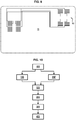
figure 10 illustre des étapes d'un procédé de fabrication d'une carte électronique selon l'invention. - Sur l'ensemble des figures les éléments similaires portent des références identiques.
- Les
figures 1a et 1b illustrent une carte électronique comprenant un corps 1 de carte et un module 2 d'empreinte. - Le corps 1 de carte comprend une surface supérieure 11 et une surface inférieure 12 et présente des dimensions conformes au standard ISO 781 ID1 En particulier, le corps 1 de carte présente une épaisseur comprise entre 780 et 840 µm.
- En outre, le corps de carte comprend plusieurs couches assemblées entre elles au moyen d'un procédé de lamination à chaud de manière à satisfaire les contraintes de tenue des couches entre elles du standard ISO 781 ID1.
- La carte électronique comprend un module 2 d'empreinte logé dans une cavité 13 formée dans l'épaisseur du corps 1 de carte. La cavité 13 débouche de la surface supérieure 11 du corps 1 de carte et affleure la surface supérieure du corps de carte. La cavité 13 est avantageusement obtenue par fraisage du corps 1 de carte sur une épaisseur souhaitée.
- Le module 2 d'empreinte est configuré pour acquérir l'image d'une empreinte d'un utilisateur et pour vérifier l'identité du porteur de la carte électronique.
- Le module 2 comprend un substrat 22 semi-conducteur et flexible typiquement en matière polymère et époxy afin d'être compatible avec les contraintes de flexibilité du standard cité tout en étant suffisamment solide.
- Une partie de ce substrat 22 constitue la partie active 21 du module sur laquelle le porteur va poser son doigt pour que l'image de son empreinte soit acquise.
- Le reste du substrat 22 permet l'assemblage du module 2 d'empreinte sur la carte et de support pour l'assemblage d'un microcontrôleur 23 (configuré pour comparer une empreinte fraichement acquise à une empreinte de référence) et éventuellement d'une mémoire 24 (qui peut comprendre une empreinte de référence de l'utilisateur préalablement stockée).
- Ainsi, le microcontrôleur est configuré pour mettre en oeuvre l'acquisition de l'empreinte ainsi que les traitements de ladite empreinte. En particulier, l'image de l'empreinte est capturée par la partie active puis traitée par le microcontrôleur de façon à extraire un modèle qui servira à la comparaison avec l'image que le porteur aura enregistré dans la carte lors d'une phase précédente d'enrôlement.
- Le module d'empreinte comprend donc un substrat 2 comprenant une face active 221 et une face de connexion 222 opposée à la face active 221. La face active 221 est la partie du module d'empreinte qui affleure la surface supérieure du corps 1 de carte et qui comprend la partie active 21.
- Par exemple, pour un module 2 d'empreintes d'une épaisseur de 600 micromètres, la face active 221 peut affleurer la surface supérieure 11 du corps 1 de carte avec une tolérance d'environ 100 micromètres, de préférence d'environ 50 micromètres.
- Une telle tolérance permet de respecter les contraintes d'introduction de la carte avec son module 2 dans un terminal de type distributeur automatique de billets, alors qu'un module 2 d'empreintes qui serait plus surélevé par rapport à la surface supérieure 11 conduirait à des difficultés, voire une impossibilité, d'introduction de la carte.
- Une telle tolérance permet également d'aboutir à une résistance structurelle et à une facilité de fabrication satisfaisantes de la carte, alors qu'un module 2 d'empreintes positionné plus bas dans l'épaisseur de la carte en fragiliserait la structure et en compliquerait la fabrication à grande échelle.
- Par ailleurs, la durée de vie d'une carte dont le module 2 serait situé plus bas dans l'épaisseur de la carte serait également réduite par l'accumulation d'impuretés et de poussières dans l'interstice entre la surface supérieure 11 et le module 2 d'empreintes, ce qui endommageraient à terme le dispositif.
- Enfin, un module 2 d'empreintes qui serait situé dans un renfoncement par rapport à la surface supérieure 11 pourrait conduire à une sensation désagréable de contrainte pour un utilisateur plaçant son doigt sur la face active 221 renfoncée. Par conséquent, un module 2 affleurant la surface supérieure 11 de la carte sera plus facilement adopté par les utilisateurs.
- De manière avantageuse, le microcontrôleur 23 est éventuellement la mémoire sont assemblés au substrat 2 typiquement par collage à froid anisotropique ou refusion au niveau de la face de connexion 222.
- La face de connexion 222 est la partie du module d'empreinte qui est dans la cavité 13 formée dans le corps 1 de carte et comprend des plots 25 de connexions qui permettent la connexion du module d'empreinte à une antenne ou bien à un autre module. Nous y reviendrons.
- On note que sur la
figure 2 quatre plots de connexions sont illustrés. Toutefois, un nombre différent peut être prévu en fonction des connexions requises. - Ces plots 25 de connexion sont disposés autour du substrat 2 de façon à perdre le moins de place possible pour la partie active 21 et le montage des composants. Néanmoins, aucune ligne de connexion et aucun composant ne doivent se trouver à moins de 0,3 mm de ces plots de façon à garantir le bon montage du module sur la carte. De plus, un renforcement sur le contour du substrat est avantageusement prévu pour éviter une trop grande flexibilité sur cette partie servant à l'assemblage. Ce renforcement peut être une couronne de matériau conducteur interne au substrat.
- La hauteur maximale du substrat et des composants doit être de 600 µm de façon à pouvoir être intégré dans la carte sans dommage et en garantissant une toile de fond suffisante pour la mise en conformité avec les exigences de flexibilité et de robustesse du standard ISO 781 ID1.
- Comme déjà mentionné, le substrat 22 de module 2 d'empreinte est flexible. Aussi, pour éviter que le substrat 22, sous l'effet des déformations générés par le doigt de l'utilisateur, ne se détériore, une fois assemblé dans la carte, on prévoit avantageusement une cavité 13 présentant un profil interne tridimensionnel en ce qu'il épouse sensiblement le profil des éléments connectés faisant saillie de la face 212 de connexion du substrat 22 du module 2 d'empreinte.
- Sur la
figure 2 , la cavité est dite « standard » sans profil particulier. Sur lafigure 3 , on montre une cavité avec le module d'empreinte se déformant lorsqu'un doigt d'un utilisateur est posé sur la partie active du module d'empreinte et sur lafigure 4 on montre une cavité présentant un profil tridimensionnel. - Les composants 23, 24 sont directement montés au-dessous du substrat 2 sur la face de connexion et participent à la limitation des déformations. De plus, le profil interne tridimensionnel de la cavité épousant sensiblement la forme du module 2 d'empreinte, cela permet d'avoir une ou plusieurs butée(s) 18 qui permettront de limiter les déformations du substrat 22 du module 2 d'empreinte.
En relation avec lafigure 5 , le corps de carte comprend l'empilement suivant depuis la surface supérieure 11 du corps de carte vers la surface inférieure 12 du corps 1 de carte : - une couche 13 supérieure de protection transparente en matière plastique ;
- un premier substrat 14 en matière plastique ;
- une couche 15 intermédiaire comprenant un matériau conducteur à base de cuivre ;
- un second substrat 16 en matière plastique ;
- une couche 17 inférieure de protection transparente en matière plastique. Les couches en plastique sont par exemple en PVC ou PC ou PET.
- Les couches en plastiques sont prévues pour supporter d'éventuelles inscriptions (visuel client, décorations diverses, identité, etc.) et les couches de protection sont prévues pour protéger les couches plastiques et recevoir des informations de personnalisation du porteur de la carte.
- La couche 15 intermédiaire est prévue pour supporter d'éventuelles pistes conductrices pour connecter le module d'empreinte à une antenne ou bien à un autre module. Cet aspect sera détaillé ultérieurement.
- De manière avantageuse, en relation avec la
figure 6 , sur la face 11 supérieure du corps de carte, la couche 13 supérieure de protection transparente comprend une marque 4 tactile qui est ajoutée au moyen de l'impression d'un vernis tactile, ou par gravure de la couche 13 supérieure de protection transparente. Cette marque tactile est mise en place au voisinage proche du capteur 21 d'empreinte (et donc du module 2 d'empreinte) de manière à guider l'utilisateur lorsqu'il pose son doigt sur le capteur 21 d'empreinte. La marque 4 tactile permet de faciliter l'acquisition de l'empreinte. - En particulier, la marque 4 tactile est telle que lorsqu'un utilisateur pose son doigt, l'empreinte à acquérir est correctement positionnée sur le capteur 21 d'empreinte.
- La marque 4 tactile est avantageusement imprimée par sérigraphie d'un vernis tactile ou gravée lors de la lamination des couches entre elles (par l'intermédiaire de plaques gravées) ou encore gravée par Laser. Elle présente une épaisseur maximale de 50 µm afin d'être compatible avec les contraintes de taille du standard ISO 781 ID1.
- Pour un module d'empreinte rectangulaire ayant une largeur entre 15 mm et 18 mm, la marque tactile est située à un distance maximale de 8-12 mm de la partie active, de préférence 10 mm.
- La forme de la marque tactile est de préférence en forme de demi-lune (voir la
figure 6 ). D'autres formes sont envisageables. - Cette marque 4 tactile présente un motif dont la rugosité est différente de celle de la surface supportant la marque.
- De manière alternative ou complémentaire, une marque 5 d'alignement permettant, le cas échéant, d'indiquer à l'utilisateur où positionner son sur le corps de carte est imprimée sur le premier substrat 14 et protégé par la couche 13 supérieure de protection transparente. La marque 5 d'alignement est typiquement une portion de cercle représentant l'extrémité d'un doigt.
- Selon un mode de réalisation, illustré sur la
figure 7 , la carte électronique est utilisée à des fins de fonctionnement par interface sans contact (par radiofréquence à courte ou moyenne portée via une antenne). L'authentification du porteur et la validation de son identité pourra déclencher, par sans contact, un accès, un paiement ou autre. L'alimentation de la carte se fait via un terminal sans contact qui communique avec la carte. Ce terminal suivant les applications est un lecteur d'accès, un terminal de paiement ou autre. - A ce titre, on prévoit une antenne 30 connectée au module 2 d'empreinte. L'antenne 30 est placée sur la couche intermédiaire et laminée dans le corps 1 de carte. Au moins un plot 25 de connexion est alors connecté à l'antenne 30 par un processus de connexion électrique via une résine conductrice ou autre. Pour permettre la connexion du module 2 d'empreinte à l'antenne 30 on prévoit au moins une cavité 41 ménagée dans le corps 1 de carte qui est remplie par exemple de résine 51 conductrice ou autre.
- Selon un fonctionnement dit « sans contact », un terminal sans contact communique avec la carte et contient une antenne. Ce terminal est alimenté et grâce au passage d'un courant alternatif dans son antenne, le terminal génère un champ magnétique alternatif. Grâce à son antenne, la carte à proximité de ce champ alternatif peut extraire son énergie. En outre, le courant alternatif du terminal est modulé à deux fréquences différentes ce qui permet de transmettre les données en même temps que l'énergie. Ainsi, recevant son énergie, la carte va démoduler le signal et retrouver en même temps les données modulées et transmises par le terminal.
- On a décrit un fonctionnement sans contact mais la carte ici décrite s'applique à des fonctionnements autres, tels que :
- avec contact (via un module d'interface classique conforme au standard ISO 7816-2) ;
- ou « dual » c'est-à-dire avec les deux moyens d'alimentation (contact ou non);
- Le protocole de communication entre terminal et carte est standardisé de façon à garantir l'interopérabilité. De tels standards sont par exemples les standards ISO 14443 et ISO 15693.
- En relation avec la
figure 8 , la carte électronique comprend, outre un module 2 d'empreinte, un deuxième module 3 comprenant une puce configurée pour opérer des fonctions par ailleurs connues de l'homme du métier telles qu'une fonction de contrôle d'accès à un lieu et/ou un réseau de transport et/ou une fonction d'identification régalienne d'individus et/ou une fonction de paiement. - Selon ce mode réalisation, l'authentification du porteur de la carte et la validation de son identité pourra déclencher, par mode contact ou sans contact, un accès, un paiement ou autre.
- Toujours en relation avec la
figure 8 , la carte comprend donc un deuxième module 3 logé dans une cavité 13' dédiée. - Le deuxième module 3 est connecté au module 2 d'empreinte via un circuit 40 placé sur la couche intermédiaire. Le module 3 comprend un microcontrôleur (puce) 31.
- Le module 2 d'empreinte et le deuxième module 3 sont connectés au circuit via des évidements 41, 42, 43, 44 ménagées dans le corps et remplis par exemple de résine 51 conductrice ou autre. Sur la
figure 8 , quatre évidements sont illustrés mais on comprendra qu'il y a autant d'évidements que nécessaires. - La
figure 9 illustre une vue détaillée de la couche d'interconnexion de la carte électronique de lafigure 8 . - Sur cette figure, on voit quatre connexions pour connecter le module 2 d'empreinte au module 3 de paiement. Bien entendu, le nombre et la disposition des connexions pourront varier en fonction du type de circuit de connexion.
- De manière complémentaire, le deuxième module 3 peut s'interfacer suivant les modes contact et sans contact (on parle de fonctionnement en mode DUAL). Dès que le mode sans contact est nécessaire, une antenne (non représentée en
figure 8 ), est placée sur la couche d'interconnexion ou est ajoutée directement au deuxième module 3. - La carte électronique ci-dessus décrite est avantageusement fabriquée au moyen d'un procédé décrit en relation avec la
figure 10 . - Le procédé de fabrication comprend essentiellement les étapes suivantes :
- obtention 100 d'un corps de carte ;
- formation 300 d'au moins une cavité 13, 13' dans le corps 1 de carte ;
- placement 400 du module 2 d'empreinte dans la cavité.
- Selon l'application de la carte électronique, l'obtention du corps 1 de carte comprend :
- une sous-étape 110 d'intégration d'une antenne 30 sur la couche intermédiaire ; et/ou
- une sous-étape 110' d'intégration d'un circuit de connexion permettant de connecter le module d'empreinte au deuxième module 3.
- L'intégration de l'antenne et/ou du circuit de connexion est mise en oeuvre au moyen d'une couche spécifique assemblée avec les autres couches du corps de carte.
- De manière avantageuse, le corps 1 de carte est obtenu (étape 120) au moyen d'un procédé de lamination des différentes couches constituant le corps 1 de carte : couches de protection, couches sur lesquelles est imprimé le visuel de la carte incluant la marque d'alignement et la couche intérieure d'inter connexion pouvant porter l'antenne pour un mode de fonctionnement dit sans contact ou DUAL.
- Les paramètres de ce procédé sont dépendants des matériaux utilisés mais et peuvent varier de températures inférieures à 100°C pendant quelques secondes à des températures de plus de 180°C pendant 20 minutes à des pressions différentes. Le but de l'opération est d'obtenir une structure homogène avec une adhésion des différentes couches entre elles conforme au standard ISO 781 ID1. Pendant ce procédé, la marque tactile peut être générée en utilisant des plaques de lamination préalablement gravées.
- Si ce n'est pas le cas pendant la lamination, de manière complémentaire, une étape d'impression de la marque tactile est mise en oeuvre. Les couches laminées entre elles sont alors imprimées à l'aide d'un vernis tactile. Le procédé utilisé est celui de la sérigraphie afin d'obtenir une épaisseur suffisante pour un obtenir un toucher tout en restant dans une épaisseur conforme au standard (50 µm). Suivant le visuel imprimé sur la carte, on peut aussi envisager d'ajouter cette marque tactile par gravure à l'aide d'un laser. Les visuels sombres seront préférés aux visuels clairs pour utiliser cette technologie maquant la matière de traces sombres.
- En outre, avant de placer le ou les modules dans les cavités formées, le procédé comprend une étape 200 d'obtention d'au moins un évidement dans le corps de carte depuis la cavité vers la couche intermédiaire. Le ou les évidements permettent d'effectuer les connexions nécessaires du ou des module(s) à la couche d'interconnexion.
Claims (15)
- Carte électronique flexible comprenant :- un corps (1) de carte comprenant une surface (11) supérieure et une surface (12) inférieure ;- au moins une cavité (13, 13') formée dans le corps de carte débouchant de la surface supérieure ;- un module (2) d'empreinte configuré pour acquérir une empreinte digitale d'un utilisateur, le module d'empreinte étant logé dans la cavité (13) et affleure la surface supérieure du corps de carte ; le module (2) d'empreinte comprenant un substrat flexible (22) comprenant une partie active (21) dite de capture affleurant la surface supérieure du corps de carte et un microcontrôleur (23) disposé au-dessous du substrat.
- Carte électronique selon la revendication 1, dans laquelle le module (2) d'empreinte comprend en outre des plots de connexion destinés à connecter ledit module d'empreinte à une antenne (30) ou à un deuxième module (3).
- Carte électronique selon l'une des revendications précédentes, dans laquelle la cavité (13, 13') présente une profondeur maximale telle que la distance entre la surface inférieure du corps de carte et le fond de la cavité est supérieur ou égal à 160 µm.
- Carte électronique selon l'une des revendications précédentes, dans laquelle la cavité (13, 13') présente un profil interne tridimensionnel de manière à suivre le relief interne du module (2) d'empreinte, la cavité comprenant au moins une butée configurée pour limiter les déformations du module logé dans la cavité.
- Carte électronique selon l'une des revendications précédentes, comprenant deux cavités (13, 13'), une cavité logeant le module d'empreinte, l'autre cavité logeant un deuxième module (3) typiquement bancaire ou d'accès.
- Carte électronique selon l'une des revendications précédentes, dans laquelle le corps (1) de carte comprend une couche intermédiaire, dite d'interconnexion, en matériau conducteur sur laquelle une antenne est intégrée.
- Carte électronique selon la revendication 5, dans laquelle le corps (1) de carte comprend une couche intermédiaire, dite d'interconnexion, en matériau semi-conducteur sur laquelle un circuit, configuré pour connecter le module d'empreinte au deuxième module (3)
- Carte électronique selon la revendication précédente, comprenant des évidements formés depuis l'au moins une cavité vers la couche d'interconnexion.
- Carte électronique selon l'une des revendications 1 à 8, dans laquelle le corps de carte comprend depuis la surface supérieure vers la surface inférieure les couches suivantes laminées :- une couche (13) supérieure de protection transparente ;- un premier substrat (14) en PVC ;- la couche (15) intermédiaire dite d'interconnexion ;- un second substrat (16) en PVC ;- une couche (17) inférieure de protection transparente.
- Carte électronique selon l'une des revendications précédentes, comprenant en outre une marque (4) tactile et/ou une marque (5) d'alignement disposée(s) sur la surface supérieure du corps de carte à proximité du module (2) d'empreinte, ladite marque tactile étant configurée pour permettre un positionnement correct d'un doigt sur le module (2) d'empreinte.
- Procédé de fabrication d'une carte électronique selon l'une des revendications précédentes, comprenant des étapes de- obtention (100) d'un corps de carte ;- formation (300) d'au moins une cavité (13, 13') dans ledit corps de carte ;- placement (400) d'un module (2) d'empreinte dans la cavité, le module (2) d'empreinte comprenant un substrat flexible (22) comprenant une partie active (21) dite de capture affleurant la surface supérieure du corps de carte et un microcontrôleur (23) disposé au-dessous du substrat.
- Procédé de fabrication selon la revendication 11, dans lequel l'étape d'obtention du corps de carte comprend une sous-étape (110) d'intégration d'une antenne sur la couche (15) intermédiaire.
- Procédé de fabrication selon l'une des revendications 11 à 12, comprenant l'obtention (200) de deux cavités dans le corps (1) de carte, et le placement (400) du module d'empreinte dans une des deux cavités et le placement d'un deuxième module (3) dans l'autre cavité, l'étape d'obtention (100) du corps (1) de carte comprend en outre une étape d'intégration (110') d'un circuit (40) de connexion configuré pour connecter le module (2) d'empreinte au deuxième module (3).
- Procédé de fabrication selon l'une des revendications 11 à 13, dans lequel l'étape (100) d'obtention du corps (1) de carte comprend une sous-étape (110) de lamination à chaud de la couche (13) supérieure, du premier substrat (14), de la couche (15) intermédiaire et de la couche (17) inférieure.
- Procédé de fabrication selon l'une des revendications 11 à 14, comprenant une étape (200) d'obtention d'au moins un évidement dans le corps de carte depuis la cavité vers la couche intermédiaire.
Priority Applications (1)
| Application Number | Priority Date | Filing Date | Title |
|---|---|---|---|
| PL18305953T PL3432221T3 (pl) | 2017-07-17 | 2018-07-13 | Karta elektroniczna zawierająca czytnik linii papilarnych i sposób wytwarzania takiej karty |
Applications Claiming Priority (1)
| Application Number | Priority Date | Filing Date | Title |
|---|---|---|---|
| FR1756763A FR3069081B1 (fr) | 2017-07-17 | 2017-07-17 | Carte electronique comprenant un capteur d'empreinte et procede de fabrication d'une telle carte |
Publications (2)
| Publication Number | Publication Date |
|---|---|
| EP3432221A1 true EP3432221A1 (fr) | 2019-01-23 |
| EP3432221B1 EP3432221B1 (fr) | 2021-11-03 |
Family
ID=60627718
Family Applications (1)
| Application Number | Title | Priority Date | Filing Date |
|---|---|---|---|
| EP18305953.4A Revoked EP3432221B1 (fr) | 2017-07-17 | 2018-07-13 | Carte électronique comprenant un capteur d'empreinte et procédé de fabrication d'une telle carte |
Country Status (6)
| Country | Link |
|---|---|
| US (1) | US10769405B2 (fr) |
| EP (1) | EP3432221B1 (fr) |
| CN (1) | CN109271835B (fr) |
| ES (1) | ES2902029T3 (fr) |
| FR (1) | FR3069081B1 (fr) |
| PL (1) | PL3432221T3 (fr) |
Cited By (1)
| Publication number | Priority date | Publication date | Assignee | Title |
|---|---|---|---|---|
| EP3646239A4 (fr) * | 2017-06-28 | 2021-03-10 | Fingerprint Cards AB | Module de capteur d'empreinte digitale comprenant une antenne et procédé de fabrication d'un module de capteur d'empreinte digitale |
Families Citing this family (11)
| Publication number | Priority date | Publication date | Assignee | Title |
|---|---|---|---|---|
| USD855617S1 (en) * | 2017-01-17 | 2019-08-06 | David Williams | Smart card |
| FR3063555B1 (fr) * | 2017-03-03 | 2021-07-09 | Linxens Holding | Carte a puce et procede de fabrication d’une carte a puce |
| SG10201902933WA (en) * | 2019-04-01 | 2020-11-27 | Advanide Holdings Pte Ltd | An improved card with fingerprint biometrics |
| CN110033071B (zh) * | 2019-04-17 | 2022-08-26 | 深圳华创兆业科技股份有限公司 | 一种指纹识别卡及其制备方法 |
| KR102790323B1 (ko) | 2019-08-23 | 2025-04-07 | 주식회사 시솔지주 | 지문 인식 카드 |
| US11893440B2 (en) | 2019-12-20 | 2024-02-06 | Linxens Holding | Card-type substrate having biometric functionality and a method of forming the same |
| FR3111215B1 (fr) * | 2020-06-04 | 2022-08-12 | Linxens Holding | Module de capteur biométrique pour carte à puce et procédé de fabrication d’un tel module |
| EP4232949B1 (fr) * | 2020-10-23 | 2026-03-25 | Visa International Service Association | Capteur biométrique intégré et mémoire pour carte biométrique |
| SE2051294A1 (en) * | 2020-11-06 | 2022-05-07 | Fingerprint Cards Anacatum Ip Ab | Integrated biometric sensor module and method for manufacturing a smartcard comprising an integrated biometric sensor module |
| TWM612841U (zh) * | 2021-02-19 | 2021-06-01 | 安帝司股份有限公司 | 指紋辨識智慧卡 |
| KR20240018865A (ko) | 2022-08-03 | 2024-02-14 | 삼성전자주식회사 | 지문 센서 패키지 및 이를 포함하는 스마트 카드 |
Citations (4)
| Publication number | Priority date | Publication date | Assignee | Title |
|---|---|---|---|---|
| US20050139685A1 (en) * | 2003-12-30 | 2005-06-30 | Douglas Kozlay | Design & method for manufacturing low-cost smartcards with embedded fingerprint authentication system modules |
| US20060097059A1 (en) * | 2004-11-08 | 2006-05-11 | Seiko Epson Corporation | IC card |
| US20090153297A1 (en) * | 2007-12-14 | 2009-06-18 | Validity Sensors, Inc. | Smart Card System With Ergonomic Fingerprint Sensor And Method of Using |
| EP3159832A1 (fr) * | 2015-10-23 | 2017-04-26 | Nxp B.V. | Jeton d'authentification |
Family Cites Families (17)
| Publication number | Priority date | Publication date | Assignee | Title |
|---|---|---|---|---|
| JP2000076412A (ja) | 1998-08-28 | 2000-03-14 | Soriton Syst:Kk | 指紋認証付電子カード及びその方法 |
| JP2001126042A (ja) | 1999-10-26 | 2001-05-11 | Toppan Printing Co Ltd | Icカード |
| JP2006134086A (ja) | 2004-11-05 | 2006-05-25 | Alps Electric Co Ltd | 指紋センサ付きicカード |
| CA2724396C (fr) | 2008-05-22 | 2015-12-01 | Cardlab Aps | Lecteur d'empreintes digitales et son procede de fonctionnement |
| HK1130618A2 (zh) * | 2008-10-30 | 2010-05-14 | 耀光联有限公司 | 一种金融交易卡 |
| NO20093601A1 (no) | 2009-12-29 | 2011-06-30 | Idex Asa | Overflatesensor |
| NO336008B1 (no) * | 2013-06-26 | 2015-04-20 | Steinar Pedersen | Enkel og pålitelig autentisering av fingeravtrykk |
| CN103400181B (zh) * | 2013-07-24 | 2016-01-20 | 江苏恒成高科信息科技有限公司 | 指纹读取传感器ic卡及其封装方法 |
| EP2869243A1 (fr) | 2013-10-31 | 2015-05-06 | Gemalto SA | Carte à puce comportant une batterie et procédé de fabrication d'une telle carte |
| EP2933759A1 (fr) | 2014-04-18 | 2015-10-21 | Gemalto SA | Procédé de fabrication d'un dispositif à circuit électronique/électrique |
| SE1451084A1 (sv) * | 2014-09-16 | 2016-03-17 | Fingerprint Cards Ab | Method and fingerprint sensing system for authenticating a candidate fingerprint |
| US9576177B2 (en) * | 2014-12-11 | 2017-02-21 | Fingerprint Cards Ab | Fingerprint sensing device |
| TW201643772A (zh) * | 2015-06-08 | 2016-12-16 | 指紋卡公司 | 具有中介結構的指紋感測裝置 |
| GB201600890D0 (en) | 2016-01-18 | 2016-03-02 | Zwipe As | Reinforced fingerprint sensor card |
| US9773153B1 (en) * | 2016-03-24 | 2017-09-26 | Fingerprint Cards Ab | Fingerprint sensor module |
| CN206312196U (zh) | 2016-10-21 | 2017-07-07 | 赵叔淋 | 具指纹辨识功能的芯片卡 |
| US10395164B2 (en) * | 2016-12-15 | 2019-08-27 | Fingerprint Cards Ab | Fingerprint sensing module and method for manufacturing the fingerprint sensing module |
-
2017
- 2017-07-17 FR FR1756763A patent/FR3069081B1/fr active Active
-
2018
- 2018-07-13 PL PL18305953T patent/PL3432221T3/pl unknown
- 2018-07-13 ES ES18305953T patent/ES2902029T3/es active Active
- 2018-07-13 EP EP18305953.4A patent/EP3432221B1/fr not_active Revoked
- 2018-07-16 CN CN201810778810.8A patent/CN109271835B/zh active Active
- 2018-07-17 US US16/038,090 patent/US10769405B2/en active Active
Patent Citations (4)
| Publication number | Priority date | Publication date | Assignee | Title |
|---|---|---|---|---|
| US20050139685A1 (en) * | 2003-12-30 | 2005-06-30 | Douglas Kozlay | Design & method for manufacturing low-cost smartcards with embedded fingerprint authentication system modules |
| US20060097059A1 (en) * | 2004-11-08 | 2006-05-11 | Seiko Epson Corporation | IC card |
| US20090153297A1 (en) * | 2007-12-14 | 2009-06-18 | Validity Sensors, Inc. | Smart Card System With Ergonomic Fingerprint Sensor And Method of Using |
| EP3159832A1 (fr) * | 2015-10-23 | 2017-04-26 | Nxp B.V. | Jeton d'authentification |
Non-Patent Citations (1)
| Title |
|---|
| SHIGEMATSU S ET AL: "A SINGLE-CHIP FINGERPRINT SENSOR AND IDENTIFIER", IEEE JOURNAL OF SOLID-STATE CIRCUITS, IEEE SERVICE CENTER, PISCATAWAY, NJ, USA, vol. 34, no. 12, 1 December 1999 (1999-12-01), pages 1852 - 1859, XP000861834, ISSN: 0018-9200, DOI: 10.1109/4.808910 * |
Cited By (1)
| Publication number | Priority date | Publication date | Assignee | Title |
|---|---|---|---|---|
| EP3646239A4 (fr) * | 2017-06-28 | 2021-03-10 | Fingerprint Cards AB | Module de capteur d'empreinte digitale comprenant une antenne et procédé de fabrication d'un module de capteur d'empreinte digitale |
Also Published As
| Publication number | Publication date |
|---|---|
| FR3069081A1 (fr) | 2019-01-18 |
| ES2902029T3 (es) | 2022-03-24 |
| US10769405B2 (en) | 2020-09-08 |
| US20190019005A1 (en) | 2019-01-17 |
| CN109271835B (zh) | 2024-03-26 |
| PL3432221T3 (pl) | 2022-01-24 |
| EP3432221B1 (fr) | 2021-11-03 |
| CN109271835A (zh) | 2019-01-25 |
| FR3069081B1 (fr) | 2021-08-20 |
Similar Documents
| Publication | Publication Date | Title |
|---|---|---|
| EP3432221B1 (fr) | Carte électronique comprenant un capteur d'empreinte et procédé de fabrication d'une telle carte | |
| EP3223199B1 (fr) | Procédé de réalisation d'un module multifonctionnel et dispositif le comprenant | |
| EP2194489A1 (fr) | Carte électronique ayant des moyens de commande | |
| EP2718877B1 (fr) | Module a microcircuit et carte a puce le comportant | |
| EP2178032B1 (fr) | Module, carte à microcircuit et procédé de fabrication correspondant | |
| EP4416636B1 (fr) | Carte à puce avec capteur biométrique | |
| EP2239691B1 (fr) | Ensemble à clé mémoire comprenant une carte à microcircuit | |
| EP3132386A1 (fr) | Procédé de fabrication d'un dispositif à circuit électronique / électrique | |
| EP3192013B1 (fr) | Dispositif électronique comportant un composant électronique présentant une zone d'affichage et procédé de fabrication d'un tel dispositif | |
| EP2410472A1 (fr) | Insert à transpondeur et dispositif comprenant un tel insert | |
| EP2045765B1 (fr) | Procédé de fabrication d'une clé électronique à connecteur USB | |
| EP2869243A1 (fr) | Carte à puce comportant une batterie et procédé de fabrication d'une telle carte | |
| EP3136303B1 (fr) | Carte et procédé de fabrication correspondant | |
| WO2014102461A1 (fr) | Carte à puce avec élément sécuritaire réparti entre corps de carte et module | |
| EP2089836B2 (fr) | Carte à microcircuit avec antenne déportée | |
| EP2202677B1 (fr) | Carte à microcircuit et terminal mobile comprenant une telle carte | |
| WO2005064533A1 (fr) | Procedes de fabrication d'une carte du type sans contacts externes, et carte ainsi obtenue | |
| EP2293226B1 (fr) | Dispositif électronique comprenant une carte à microcircuit | |
| FR3095531A1 (fr) | Etiquette de garantie et de test d’un capteur biométrique, dispositif électronique tel une carte à puce, procédés de fabrication et de test | |
| EP2095301A1 (fr) | Cartes à microcircuit pour antenne déportée et antennes déportées |
Legal Events
| Date | Code | Title | Description |
|---|---|---|---|
| PUAI | Public reference made under article 153(3) epc to a published international application that has entered the european phase |
Free format text: ORIGINAL CODE: 0009012 |
|
| STAA | Information on the status of an ep patent application or granted ep patent |
Free format text: STATUS: THE APPLICATION HAS BEEN PUBLISHED |
|
| AK | Designated contracting states |
Kind code of ref document: A1 Designated state(s): AL AT BE BG CH CY CZ DE DK EE ES FI FR GB GR HR HU IE IS IT LI LT LU LV MC MK MT NL NO PL PT RO RS SE SI SK SM TR |
|
| AX | Request for extension of the european patent |
Extension state: BA ME |
|
| STAA | Information on the status of an ep patent application or granted ep patent |
Free format text: STATUS: REQUEST FOR EXAMINATION WAS MADE |
|
| 17P | Request for examination filed |
Effective date: 20190712 |
|
| RBV | Designated contracting states (corrected) |
Designated state(s): AL AT BE BG CH CY CZ DE DK EE ES FI FR GB GR HR HU IE IS IT LI LT LU LV MC MK MT NL NO PL PT RO RS SE SI SK SM TR |
|
| RIC1 | Information provided on ipc code assigned before grant |
Ipc: G06K 19/077 20060101ALI20210430BHEP Ipc: G06K 19/07 20060101AFI20210430BHEP |
|
| GRAP | Despatch of communication of intention to grant a patent |
Free format text: ORIGINAL CODE: EPIDOSNIGR1 |
|
| STAA | Information on the status of an ep patent application or granted ep patent |
Free format text: STATUS: GRANT OF PATENT IS INTENDED |
|
| INTG | Intention to grant announced |
Effective date: 20210617 |
|
| GRAS | Grant fee paid |
Free format text: ORIGINAL CODE: EPIDOSNIGR3 |
|
| GRAA | (expected) grant |
Free format text: ORIGINAL CODE: 0009210 |
|
| STAA | Information on the status of an ep patent application or granted ep patent |
Free format text: STATUS: THE PATENT HAS BEEN GRANTED |
|
| AK | Designated contracting states |
Kind code of ref document: B1 Designated state(s): AL AT BE BG CH CY CZ DE DK EE ES FI FR GB GR HR HU IE IS IT LI LT LU LV MC MK MT NL NO PL PT RO RS SE SI SK SM TR |
|
| REG | Reference to a national code |
Ref country code: GB Ref legal event code: FG4D Free format text: NOT ENGLISH |
|
| REG | Reference to a national code |
Ref country code: AT Ref legal event code: REF Ref document number: 1444637 Country of ref document: AT Kind code of ref document: T Effective date: 20211115 Ref country code: CH Ref legal event code: EP |
|
| REG | Reference to a national code |
Ref country code: IE Ref legal event code: FG4D Free format text: LANGUAGE OF EP DOCUMENT: FRENCH |
|
| REG | Reference to a national code |
Ref country code: DE Ref legal event code: R096 Ref document number: 602018026037 Country of ref document: DE |
|
| REG | Reference to a national code |
Ref country code: NL Ref legal event code: FP |
|
| REG | Reference to a national code |
Ref country code: LT Ref legal event code: MG9D |
|
| REG | Reference to a national code |
Ref country code: ES Ref legal event code: FG2A Ref document number: 2902029 Country of ref document: ES Kind code of ref document: T3 Effective date: 20220324 |
|
| PG25 | Lapsed in a contracting state [announced via postgrant information from national office to epo] |
Ref country code: RS Free format text: LAPSE BECAUSE OF FAILURE TO SUBMIT A TRANSLATION OF THE DESCRIPTION OR TO PAY THE FEE WITHIN THE PRESCRIBED TIME-LIMIT Effective date: 20211103 Ref country code: LT Free format text: LAPSE BECAUSE OF FAILURE TO SUBMIT A TRANSLATION OF THE DESCRIPTION OR TO PAY THE FEE WITHIN THE PRESCRIBED TIME-LIMIT Effective date: 20211103 Ref country code: FI Free format text: LAPSE BECAUSE OF FAILURE TO SUBMIT A TRANSLATION OF THE DESCRIPTION OR TO PAY THE FEE WITHIN THE PRESCRIBED TIME-LIMIT Effective date: 20211103 Ref country code: BG Free format text: LAPSE BECAUSE OF FAILURE TO SUBMIT A TRANSLATION OF THE DESCRIPTION OR TO PAY THE FEE WITHIN THE PRESCRIBED TIME-LIMIT Effective date: 20220203 |
|
| PG25 | Lapsed in a contracting state [announced via postgrant information from national office to epo] |
Ref country code: IS Free format text: LAPSE BECAUSE OF FAILURE TO SUBMIT A TRANSLATION OF THE DESCRIPTION OR TO PAY THE FEE WITHIN THE PRESCRIBED TIME-LIMIT Effective date: 20220303 Ref country code: SE Free format text: LAPSE BECAUSE OF FAILURE TO SUBMIT A TRANSLATION OF THE DESCRIPTION OR TO PAY THE FEE WITHIN THE PRESCRIBED TIME-LIMIT Effective date: 20211103 Ref country code: PT Free format text: LAPSE BECAUSE OF FAILURE TO SUBMIT A TRANSLATION OF THE DESCRIPTION OR TO PAY THE FEE WITHIN THE PRESCRIBED TIME-LIMIT Effective date: 20220303 Ref country code: NO Free format text: LAPSE BECAUSE OF FAILURE TO SUBMIT A TRANSLATION OF THE DESCRIPTION OR TO PAY THE FEE WITHIN THE PRESCRIBED TIME-LIMIT Effective date: 20220203 Ref country code: LV Free format text: LAPSE BECAUSE OF FAILURE TO SUBMIT A TRANSLATION OF THE DESCRIPTION OR TO PAY THE FEE WITHIN THE PRESCRIBED TIME-LIMIT Effective date: 20211103 Ref country code: HR Free format text: LAPSE BECAUSE OF FAILURE TO SUBMIT A TRANSLATION OF THE DESCRIPTION OR TO PAY THE FEE WITHIN THE PRESCRIBED TIME-LIMIT Effective date: 20211103 Ref country code: GR Free format text: LAPSE BECAUSE OF FAILURE TO SUBMIT A TRANSLATION OF THE DESCRIPTION OR TO PAY THE FEE WITHIN THE PRESCRIBED TIME-LIMIT Effective date: 20220204 |
|
| PG25 | Lapsed in a contracting state [announced via postgrant information from national office to epo] |
Ref country code: SM Free format text: LAPSE BECAUSE OF FAILURE TO SUBMIT A TRANSLATION OF THE DESCRIPTION OR TO PAY THE FEE WITHIN THE PRESCRIBED TIME-LIMIT Effective date: 20211103 Ref country code: SK Free format text: LAPSE BECAUSE OF FAILURE TO SUBMIT A TRANSLATION OF THE DESCRIPTION OR TO PAY THE FEE WITHIN THE PRESCRIBED TIME-LIMIT Effective date: 20211103 Ref country code: RO Free format text: LAPSE BECAUSE OF FAILURE TO SUBMIT A TRANSLATION OF THE DESCRIPTION OR TO PAY THE FEE WITHIN THE PRESCRIBED TIME-LIMIT Effective date: 20211103 Ref country code: EE Free format text: LAPSE BECAUSE OF FAILURE TO SUBMIT A TRANSLATION OF THE DESCRIPTION OR TO PAY THE FEE WITHIN THE PRESCRIBED TIME-LIMIT Effective date: 20211103 Ref country code: DK Free format text: LAPSE BECAUSE OF FAILURE TO SUBMIT A TRANSLATION OF THE DESCRIPTION OR TO PAY THE FEE WITHIN THE PRESCRIBED TIME-LIMIT Effective date: 20211103 Ref country code: CZ Free format text: LAPSE BECAUSE OF FAILURE TO SUBMIT A TRANSLATION OF THE DESCRIPTION OR TO PAY THE FEE WITHIN THE PRESCRIBED TIME-LIMIT Effective date: 20211103 |
|
| PGFP | Annual fee paid to national office [announced via postgrant information from national office to epo] |
Ref country code: NL Payment date: 20220621 Year of fee payment: 5 Ref country code: IT Payment date: 20220621 Year of fee payment: 5 Ref country code: GB Payment date: 20220621 Year of fee payment: 5 |
|
| REG | Reference to a national code |
Ref country code: DE Ref legal event code: R026 Ref document number: 602018026037 Country of ref document: DE |
|
| PLBI | Opposition filed |
Free format text: ORIGINAL CODE: 0009260 |
|
| PLAX | Notice of opposition and request to file observation + time limit sent |
Free format text: ORIGINAL CODE: EPIDOSNOBS2 |
|
| PGFP | Annual fee paid to national office [announced via postgrant information from national office to epo] |
Ref country code: PL Payment date: 20220621 Year of fee payment: 5 |
|
| 26 | Opposition filed |
Opponent name: GIESECKE+DEVRIENT MOBILE SECURITY GMBH Effective date: 20220729 |
|
| PGFP | Annual fee paid to national office [announced via postgrant information from national office to epo] |
Ref country code: FR Payment date: 20220622 Year of fee payment: 5 |
|
| RDAF | Communication despatched that patent is revoked |
Free format text: ORIGINAL CODE: EPIDOSNREV1 |
|
| PG25 | Lapsed in a contracting state [announced via postgrant information from national office to epo] |
Ref country code: AL Free format text: LAPSE BECAUSE OF FAILURE TO SUBMIT A TRANSLATION OF THE DESCRIPTION OR TO PAY THE FEE WITHIN THE PRESCRIBED TIME-LIMIT Effective date: 20211103 |
|
| PGFP | Annual fee paid to national office [announced via postgrant information from national office to epo] |
Ref country code: ES Payment date: 20220801 Year of fee payment: 5 Ref country code: DE Payment date: 20220621 Year of fee payment: 5 |
|
| REG | Reference to a national code |
Ref country code: DE Ref legal event code: R103 Ref document number: 602018026037 Country of ref document: DE Ref country code: DE Ref legal event code: R064 Ref document number: 602018026037 Country of ref document: DE |
|
| PG25 | Lapsed in a contracting state [announced via postgrant information from national office to epo] |
Ref country code: SI Free format text: LAPSE BECAUSE OF FAILURE TO SUBMIT A TRANSLATION OF THE DESCRIPTION OR TO PAY THE FEE WITHIN THE PRESCRIBED TIME-LIMIT Effective date: 20211103 |
|
| RDAG | Patent revoked |
Free format text: ORIGINAL CODE: 0009271 |
|
| STAA | Information on the status of an ep patent application or granted ep patent |
Free format text: STATUS: PATENT REVOKED |
|
| PG25 | Lapsed in a contracting state [announced via postgrant information from national office to epo] |
Ref country code: MC Free format text: LAPSE BECAUSE OF FAILURE TO SUBMIT A TRANSLATION OF THE DESCRIPTION OR TO PAY THE FEE WITHIN THE PRESCRIBED TIME-LIMIT Effective date: 20211103 |
|
| REG | Reference to a national code |
Ref country code: CH Ref legal event code: PL |
|
| 27W | Patent revoked |
Effective date: 20221031 |
|
| GBPR | Gb: patent revoked under art. 102 of the ep convention designating the uk as contracting state |
Effective date: 20221031 |
|
| REG | Reference to a national code |
Ref country code: CH Ref legal event code: PL |
|
| REG | Reference to a national code |
Ref country code: BE Ref legal event code: MM Effective date: 20220731 |
|
| PG25 | Lapsed in a contracting state [announced via postgrant information from national office to epo] |
Ref country code: LU Free format text: LAPSE BECAUSE OF NON-PAYMENT OF DUE FEES Effective date: 20220713 Ref country code: LI Free format text: LAPSE BECAUSE OF NON-PAYMENT OF DUE FEES Effective date: 20220731 Ref country code: CH Free format text: LAPSE BECAUSE OF NON-PAYMENT OF DUE FEES Effective date: 20220731 |
|
| REG | Reference to a national code |
Ref country code: AT Ref legal event code: MA03 Ref document number: 1444637 Country of ref document: AT Kind code of ref document: T Effective date: 20221031 |
|
| PG25 | Lapsed in a contracting state [announced via postgrant information from national office to epo] |
Ref country code: BE Free format text: LAPSE BECAUSE OF NON-PAYMENT OF DUE FEES Effective date: 20220731 |
|
| PG25 | Lapsed in a contracting state [announced via postgrant information from national office to epo] |
Ref country code: MK Free format text: LAPSE BECAUSE OF FAILURE TO SUBMIT A TRANSLATION OF THE DESCRIPTION OR TO PAY THE FEE WITHIN THE PRESCRIBED TIME-LIMIT Effective date: 20211103 Ref country code: CY Free format text: LAPSE BECAUSE OF FAILURE TO SUBMIT A TRANSLATION OF THE DESCRIPTION OR TO PAY THE FEE WITHIN THE PRESCRIBED TIME-LIMIT Effective date: 20211103 |
|
| PG25 | Lapsed in a contracting state [announced via postgrant information from national office to epo] |
Ref country code: IE Free format text: LAPSE BECAUSE OF NON-PAYMENT OF DUE FEES Effective date: 20220713 |
|
| PG25 | Lapsed in a contracting state [announced via postgrant information from national office to epo] |
Ref country code: TR Free format text: LAPSE BECAUSE OF FAILURE TO SUBMIT A TRANSLATION OF THE DESCRIPTION OR TO PAY THE FEE WITHIN THE PRESCRIBED TIME-LIMIT Effective date: 20211103 Ref country code: IE Free format text: LAPSE BECAUSE OF NON-PAYMENT OF DUE FEES Effective date: 20220713 |
|
| PG25 | Lapsed in a contracting state [announced via postgrant information from national office to epo] |
Ref country code: HU Free format text: LAPSE BECAUSE OF FAILURE TO SUBMIT A TRANSLATION OF THE DESCRIPTION OR TO PAY THE FEE WITHIN THE PRESCRIBED TIME-LIMIT; INVALID AB INITIO Effective date: 20180713 |
|
| REG | Reference to a national code |
Ref country code: AT Ref legal event code: UEP Ref document number: 1444637 Country of ref document: AT Kind code of ref document: T Effective date: 20211103 |
|
| PGFP | Annual fee paid to national office [announced via postgrant information from national office to epo] |
Ref country code: AT Payment date: 20260410 Year of fee payment: 5 |