EP3424147B1 - A variable frequency rc oscillator - Google Patents
A variable frequency rc oscillator Download PDFInfo
- Publication number
- EP3424147B1 EP3424147B1 EP17706649.5A EP17706649A EP3424147B1 EP 3424147 B1 EP3424147 B1 EP 3424147B1 EP 17706649 A EP17706649 A EP 17706649A EP 3424147 B1 EP3424147 B1 EP 3424147B1
- Authority
- EP
- European Patent Office
- Prior art keywords
- delay
- delay section
- output
- network
- variable capacitor
- Prior art date
- Legal status (The legal status is an assumption and is not a legal conclusion. Google has not performed a legal analysis and makes no representation as to the accuracy of the status listed.)
- Active
Links
Images


Classifications
-
- H—ELECTRICITY
- H03—ELECTRONIC CIRCUITRY
- H03B—GENERATION OF OSCILLATIONS, DIRECTLY OR BY FREQUENCY-CHANGING, BY CIRCUITS EMPLOYING ACTIVE ELEMENTS WHICH OPERATE IN A NON-SWITCHING MANNER; GENERATION OF NOISE BY SUCH CIRCUITS
- H03B5/00—Generation of oscillations using amplifier with regenerative feedback from output to input
- H03B5/20—Generation of oscillations using amplifier with regenerative feedback from output to input with frequency-determining element comprising resistance and either capacitance or inductance, e.g. phase-shift oscillator
- H03B5/24—Generation of oscillations using amplifier with regenerative feedback from output to input with frequency-determining element comprising resistance and either capacitance or inductance, e.g. phase-shift oscillator active element in amplifier being semiconductor device
-
- H—ELECTRICITY
- H03—ELECTRONIC CIRCUITRY
- H03B—GENERATION OF OSCILLATIONS, DIRECTLY OR BY FREQUENCY-CHANGING, BY CIRCUITS EMPLOYING ACTIVE ELEMENTS WHICH OPERATE IN A NON-SWITCHING MANNER; GENERATION OF NOISE BY SUCH CIRCUITS
- H03B5/00—Generation of oscillations using amplifier with regenerative feedback from output to input
- H03B5/20—Generation of oscillations using amplifier with regenerative feedback from output to input with frequency-determining element comprising resistance and either capacitance or inductance, e.g. phase-shift oscillator
- H03B5/26—Generation of oscillations using amplifier with regenerative feedback from output to input with frequency-determining element comprising resistance and either capacitance or inductance, e.g. phase-shift oscillator frequency-determining element being part of bridge circuit in closed ring around which signal is transmitted; frequency-determining element being connected via a bridge circuit to such a closed ring, e.g. Wien-Bridge oscillator, parallel-T oscillator
-
- H—ELECTRICITY
- H03—ELECTRONIC CIRCUITRY
- H03K—PULSE TECHNIQUE
- H03K3/00—Circuits for generating electric pulses; Monostable, bistable or multistable circuits
- H03K3/02—Generators characterised by the type of circuit or by the means used for producing pulses
- H03K3/027—Generators characterised by the type of circuit or by the means used for producing pulses by the use of logic circuits, with internal or external positive feedback
- H03K3/03—Astable circuits
- H03K3/0315—Ring oscillators
-
- H—ELECTRICITY
- H03—ELECTRONIC CIRCUITRY
- H03K—PULSE TECHNIQUE
- H03K5/00—Manipulating of pulses not covered by one of the other main groups of this subclass
- H03K5/01—Shaping pulses
- H03K5/04—Shaping pulses by increasing duration; by decreasing duration
- H03K5/06—Shaping pulses by increasing duration; by decreasing duration by the use of delay lines or other analogue delay elements
- H03K5/065—Shaping pulses by increasing duration; by decreasing duration by the use of delay lines or other analogue delay elements using dispersive delay lines
-
- H—ELECTRICITY
- H03—ELECTRONIC CIRCUITRY
- H03K—PULSE TECHNIQUE
- H03K5/00—Manipulating of pulses not covered by one of the other main groups of this subclass
- H03K5/125—Discriminating pulses
- H03K5/1252—Suppression or limitation of noise or interference
-
- H—ELECTRICITY
- H03—ELECTRONIC CIRCUITRY
- H03L—AUTOMATIC CONTROL, STARTING, SYNCHRONISATION OR STABILISATION OF GENERATORS OF ELECTRONIC OSCILLATIONS OR PULSES
- H03L7/00—Automatic control of frequency or phase; Synchronisation
- H03L7/06—Automatic control of frequency or phase; Synchronisation using a reference signal applied to a frequency- or phase-locked loop
- H03L7/08—Details of the phase-locked loop
- H03L7/099—Details of the phase-locked loop concerning mainly the controlled oscillator of the loop
Definitions
- an oscillator circuit having a programmable output frequency comprises a first delay section having an input end and an output end.
- the first delay section has a negative gain between the input end and the output end and a variable delay that is set by a control signal provided to the first delay section.
- the oscillator further comprises a second delay section electrically connected in series with the first delay section.
- the second delay section has an input end and an output end and a negative gain between the input end and the output end.
- the second delay section has a fixed delay.
- the oscillator further comprises a circuit output for an output signal having a frequency that is a function of the delay due to the first delay section and the second delay section.
- the circuit output comprises the output end of the second delay section.
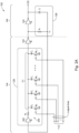
- the delay stage 128 may comprise an RC network comprising a resistor R and a capacitor C.
- Terminal ⁇ of the delay stage 128 may be connected to the resistor R and capacitor C may be connected to terminal ⁇ .
- Terminal y of the delay stage 128 may be connected to a node V X to which resistor R and capacitor C are connected.
- the delay ⁇ 1 of the RC network is generally a function of a time constant (sometimes referred to as the RC time constant) defined as R ⁇ C , which represent respective element values of resistor R and capacitor C.
- resistor R and capacitor C may be fixed-value elements. Accordingly, the delay stage 128 may provide a fixed delay.
- FIG. 2 shows additional details for delay stage 126 of the first delay section 104 in accordance with some embodiments of the present disclosure.
- the delay stage 126 may comprise a high input impedance non-inverting input buffer 202 and a variable RC network 204.
- the supply (not shown) for input buffer 202 may be the V DD supply provided to the delay stage 126, as illustrated in FIG. 1A for example.
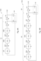
- capacitive elements Cx may be realized using any semiconductor technology suitable for a given application of the oscillator circuit 102.
- capacitive elements Cx may be PN junction capacitors, MOSFET gate capacitors, metal-insulator-metal (MIM) capacitors, metal-oxide-metal (MOM) capacitors, and so on.
- the capacitive elements Cx may be based on the same semiconductor technology, or they may be based on different technologies.
- each of the capacitive elements Cx may have the same capacitance. In other embodiments, the capacitive elements Cx may have different capacitances.
- resistor R 1 may be a fixed value element such as shown in FIG. 2A . In other embodiments (not shown), resistor R 1 may be a variable resistor and capacitor C 1 may be a fixed value element. In still other embodiments, resistor R 1 may be a variable resistor and capacitor C 1 may be a variable capacitor.
- the capacitive elements C y may be selectively switched to ground potential via a set of corresponding switches M 0 - M m-1 .
- the switches M 0 - M m-1 may be any suitable switching device.
- the switches M 0 - M m-1 may be semiconductor switches such as PNP transistors shown in FIG. 3A , for example.
- all the switches M 0 - M m-1 may be based on the same technology, or may they may be based on different technologies.
- Each of the m signal lines that comprise the selector input 312 may be connected to a respective one of the switches M 0 - M m-1 .
- the input to selector input 312 may be generated by digital logic or other suitable circuitry associated with the oscillator circuit 102 or with electronic circuit 10 ( FIG. 1A ).
- resistor R 2 may be a fixed value element such as shown in FIG. 3A . In other embodiments (not shown), resistor R 2 may be a variable resistor and capacitor C 2 may be a fixed value element. In still other embodiments (not shown), resistor R 2 may be a variable resistor and capacitor C 2 may be a variable capacitor.
- the selector inputs 112, 312 of respective delay stages 126, 326 may receive the same selection input; e.g., the same n-bit code may be provided to each selector input 112, 312. In other embodiments, each selector input 112, 312 may receive different selection inputs.
- the frequency of oscillation in oscillator circuit 102 may be controlled according to the delays ⁇ 1 , ⁇ 2 , and ⁇ 3 .
- the delay ⁇ 1 in delay stage 128 may be fixed for resistor R and capacitor C.
- the delay ⁇ 2 of the delay stage 126 may be set by asserting appropriate bit lines that comprise selector input 112 for the delay stage 126.
- the delay ⁇ 3 in delay stage 326 may be set by asserting appropriate bit lines that comprise selector signal 312. Accordingly, the frequency of the clock signal 132 may be selected as a function of the variable delays ⁇ 2 and ⁇ 3 .
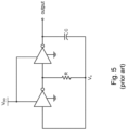
- Programmable capacitors can be difficult, since the capacitor C is a "floating" capacitor because of the behavior at node V X .
- the node V X is a floating node because the voltage at node V X may swing above and below the supply voltage in one half of a cycle of the output and above and below ground potential in the other half of the cycle.
- Programmable capacitors typically comprise a bank of switched capacitor elements. When the source (or drain) of a switch is connected at the node V X , the state of the switch can become forward biased during portions of the cycle and conduct when it is supposed to be in an OFF (non-conducting) state.
Landscapes
- Physics & Mathematics (AREA)
- Nonlinear Science (AREA)
- Inductance-Capacitance Distribution Constants And Capacitance-Resistance Oscillators (AREA)
- Pulse Circuits (AREA)
- Semiconductor Integrated Circuits (AREA)
Applications Claiming Priority (3)
| Application Number | Priority Date | Filing Date | Title |
|---|---|---|---|
| US201662302735P | 2016-03-02 | 2016-03-02 | |
| US15/191,350 US9755575B1 (en) | 2016-03-02 | 2016-06-23 | Variable frequency RC oscillator |
| PCT/US2017/017518 WO2017151295A1 (en) | 2016-03-02 | 2017-02-10 | A variable frequency rc oscillator |
Publications (2)
| Publication Number | Publication Date |
|---|---|
| EP3424147A1 EP3424147A1 (en) | 2019-01-09 |
| EP3424147B1 true EP3424147B1 (en) | 2024-07-10 |
Family
ID=59702466
Family Applications (1)
| Application Number | Title | Priority Date | Filing Date |
|---|---|---|---|
| EP17706649.5A Active EP3424147B1 (en) | 2016-03-02 | 2017-02-10 | A variable frequency rc oscillator |
Country Status (6)
| Country | Link |
|---|---|
| US (1) | US9755575B1 (enExample) |
| EP (1) | EP3424147B1 (enExample) |
| JP (1) | JP2019511168A (enExample) |
| KR (1) | KR20180118137A (enExample) |
| CN (1) | CN108781070B (enExample) |
| WO (1) | WO2017151295A1 (enExample) |
Families Citing this family (4)
| Publication number | Priority date | Publication date | Assignee | Title |
|---|---|---|---|---|
| US10873325B2 (en) * | 2018-10-12 | 2020-12-22 | Texas Instruments Incorporated | Robust noise immune, low-skew, pulse width retainable glitch-filter |
| TWI675280B (zh) * | 2018-10-25 | 2019-10-21 | 新唐科技股份有限公司 | 時脈產生電路及其時脈調整方法 |
| GB2583353B (en) | 2019-04-24 | 2023-04-12 | Pragmatic Printing Ltd | An oscillator with improved frequency stability |
| US11811364B2 (en) | 2021-06-22 | 2023-11-07 | Samsung Electronics Co., Ltd. | Clock integrated circuit including heterogeneous oscillators and apparatus including the clock integrated circuit |
Citations (3)
| Publication number | Priority date | Publication date | Assignee | Title |
|---|---|---|---|---|
| US4316158A (en) * | 1979-01-17 | 1982-02-16 | Nippon Soken, Inc. | R-C Oscillators using plural inverters |
| US20020149087A1 (en) * | 2001-03-13 | 2002-10-17 | Fujitsu Limited | Semiconductor filter system and signal frequency control method |
| JP2006261833A (ja) * | 2005-03-15 | 2006-09-28 | Sanyo Electric Co Ltd | リング発振器 |
Family Cites Families (16)
| Publication number | Priority date | Publication date | Assignee | Title |
|---|---|---|---|---|
| JPS54181853U (enExample) * | 1978-06-12 | 1979-12-22 | ||
| JPS60100819A (ja) * | 1984-10-01 | 1985-06-04 | Fujitsu General Ltd | 発振回路 |
| US5519265A (en) | 1993-05-24 | 1996-05-21 | Latham, Ii; Paul W. | Adaptive RC product control in an analog-signal-manipulating circuit |
| US5552748A (en) | 1995-06-07 | 1996-09-03 | American Microsystems, Inc. | Digitally-tuned oscillator including a self-calibrating RC oscillator circuit |
| US6737926B2 (en) * | 2001-08-30 | 2004-05-18 | Micron Technology, Inc. | Method and apparatus for providing clock signals at different locations with minimal clock skew |
| DE10345236B3 (de) * | 2003-09-29 | 2005-03-10 | Infineon Technologies Ag | Verzögerungsregelkreis |
| US7245519B2 (en) | 2005-08-22 | 2007-07-17 | Freescale Semiconductor, Inc. | Digitally programmable capacitor array |
| JP2007081593A (ja) * | 2005-09-13 | 2007-03-29 | Neuro Solution Corp | 発振器、pll回路および受信機、送信機 |
| KR20070081532A (ko) * | 2006-02-13 | 2007-08-17 | 엘지전자 주식회사 | Rc 발진회로 |
| US7605668B2 (en) | 2006-12-12 | 2009-10-20 | Intel Corporation | Delay stage with controllably variable capacitive load |
| CN102006057B (zh) * | 2009-09-01 | 2013-05-08 | 杭州中科微电子有限公司 | 可编程调整起振条件的低功耗、快速起振晶体振荡器模块 |
| US8222966B2 (en) * | 2010-09-10 | 2012-07-17 | Intel Corporation | System, method and apparatus for an open loop calibrated phase wrapping phase modulator for wideband RF outphasing/polar transmitters |
| JP5807508B2 (ja) * | 2011-10-24 | 2015-11-10 | 株式会社ソシオネクスト | 発振回路を有するマイクロコントローラ |
| WO2013141837A1 (en) | 2012-03-19 | 2013-09-26 | Taner Sumesaglam | Self-biased oscillator |
| US9584133B2 (en) | 2012-05-31 | 2017-02-28 | Silicon Laboratories Inc. | Temperature compensated oscillator with improved noise performance |
| CN104935294B (zh) * | 2014-03-20 | 2018-07-20 | 晶宏半导体股份有限公司 | 振荡器 |
-
2016
- 2016-06-23 US US15/191,350 patent/US9755575B1/en active Active
-
2017
- 2017-02-10 WO PCT/US2017/017518 patent/WO2017151295A1/en not_active Ceased
- 2017-02-10 JP JP2018545918A patent/JP2019511168A/ja active Pending
- 2017-02-10 EP EP17706649.5A patent/EP3424147B1/en active Active
- 2017-02-10 CN CN201780014246.6A patent/CN108781070B/zh not_active Expired - Fee Related
- 2017-02-10 KR KR1020187025097A patent/KR20180118137A/ko not_active Withdrawn
Patent Citations (3)
| Publication number | Priority date | Publication date | Assignee | Title |
|---|---|---|---|---|
| US4316158A (en) * | 1979-01-17 | 1982-02-16 | Nippon Soken, Inc. | R-C Oscillators using plural inverters |
| US20020149087A1 (en) * | 2001-03-13 | 2002-10-17 | Fujitsu Limited | Semiconductor filter system and signal frequency control method |
| JP2006261833A (ja) * | 2005-03-15 | 2006-09-28 | Sanyo Electric Co Ltd | リング発振器 |
Also Published As
| Publication number | Publication date |
|---|---|
| CN108781070A (zh) | 2018-11-09 |
| KR20180118137A (ko) | 2018-10-30 |
| US20170257065A1 (en) | 2017-09-07 |
| JP2019511168A (ja) | 2019-04-18 |
| EP3424147A1 (en) | 2019-01-09 |
| US9755575B1 (en) | 2017-09-05 |
| WO2017151295A1 (en) | 2017-09-08 |
| CN108781070B (zh) | 2022-05-17 |
Similar Documents
| Publication | Publication Date | Title |
|---|---|---|
| US8222962B2 (en) | High-resolution digitally controlled oscillator and method thereof | |
| JP5229218B2 (ja) | スイッチング容量生成回路、電圧制御発振器、及びlcバンドパスフィルター | |
| KR100684050B1 (ko) | 지연회로및그것을이용한발진회로 | |
| US8031011B2 (en) | Digitally controlled oscillators | |
| EP3424147B1 (en) | A variable frequency rc oscillator | |
| US6486719B2 (en) | Flip-flop circuits having digital-to-time conversion latches therein | |
| US8610511B1 (en) | High-frequency digitally controlled oscillator | |
| WO2002056469A2 (en) | Ring vco based on rc timing | |
| US8466729B2 (en) | Delay cell and digitally controlled oscillator | |
| US6509803B2 (en) | Voltage-controlled oscillator having short synchronous pull-in time | |
| CN114079424A (zh) | 可控制工作周期的倍频电路及其方法 | |
| CN115149943B (zh) | 分频电路 | |
| US11942944B2 (en) | Oscillator with improved frequency stability | |
| JP3718932B2 (ja) | 中間位相クロック生成回路 | |
| US12470173B2 (en) | Oscillator apparatus and control method | |
| JP4010328B2 (ja) | 遅延回路 | |
| CN111835338A (zh) | 电平移位器装置及操作电平移位电路的方法 | |
| US6965273B2 (en) | Oscillator with improved parameters variation tolerance | |
| KR20230029512A (ko) | 2상 클록 생성 회로 | |
| JP4238931B2 (ja) | 発振回路 | |
| TW202541417A (zh) | 振盪器裝置及控制方法 | |
| JP2006060874A (ja) | 発振回路 |
Legal Events
| Date | Code | Title | Description |
|---|---|---|---|
| STAA | Information on the status of an ep patent application or granted ep patent |
Free format text: STATUS: UNKNOWN |
|
| STAA | Information on the status of an ep patent application or granted ep patent |
Free format text: STATUS: THE INTERNATIONAL PUBLICATION HAS BEEN MADE |
|
| PUAI | Public reference made under article 153(3) epc to a published international application that has entered the european phase |
Free format text: ORIGINAL CODE: 0009012 |
|
| STAA | Information on the status of an ep patent application or granted ep patent |
Free format text: STATUS: REQUEST FOR EXAMINATION WAS MADE |
|
| 17P | Request for examination filed |
Effective date: 20180802 |
|
| AK | Designated contracting states |
Kind code of ref document: A1 Designated state(s): AL AT BE BG CH CY CZ DE DK EE ES FI FR GB GR HR HU IE IS IT LI LT LU LV MC MK MT NL NO PL PT RO RS SE SI SK SM TR |
|
| AX | Request for extension of the european patent |
Extension state: BA ME |
|
| DAV | Request for validation of the european patent (deleted) | ||
| DAX | Request for extension of the european patent (deleted) | ||
| STAA | Information on the status of an ep patent application or granted ep patent |
Free format text: STATUS: EXAMINATION IS IN PROGRESS |
|
| 17Q | First examination report despatched |
Effective date: 20210224 |
|
| GRAP | Despatch of communication of intention to grant a patent |
Free format text: ORIGINAL CODE: EPIDOSNIGR1 |
|
| STAA | Information on the status of an ep patent application or granted ep patent |
Free format text: STATUS: GRANT OF PATENT IS INTENDED |
|
| INTG | Intention to grant announced |
Effective date: 20240213 |
|
| GRAS | Grant fee paid |
Free format text: ORIGINAL CODE: EPIDOSNIGR3 |
|
| GRAA | (expected) grant |
Free format text: ORIGINAL CODE: 0009210 |
|
| STAA | Information on the status of an ep patent application or granted ep patent |
Free format text: STATUS: THE PATENT HAS BEEN GRANTED |
|
| AK | Designated contracting states |
Kind code of ref document: B1 Designated state(s): AL AT BE BG CH CY CZ DE DK EE ES FI FR GB GR HR HU IE IS IT LI LT LU LV MC MK MT NL NO PL PT RO RS SE SI SK SM TR |
|
| REG | Reference to a national code |
Ref country code: CH Ref legal event code: EP |
|
| REG | Reference to a national code |
Ref country code: DE Ref legal event code: R096 Ref document number: 602017083166 Country of ref document: DE |
|
| REG | Reference to a national code |
Ref country code: LT Ref legal event code: MG9D |
|
| REG | Reference to a national code |
Ref country code: NL Ref legal event code: MP Effective date: 20240710 |
|
| PG25 | Lapsed in a contracting state [announced via postgrant information from national office to epo] |
Ref country code: PT Free format text: LAPSE BECAUSE OF FAILURE TO SUBMIT A TRANSLATION OF THE DESCRIPTION OR TO PAY THE FEE WITHIN THE PRESCRIBED TIME-LIMIT Effective date: 20241111 |
|
| REG | Reference to a national code |
Ref country code: AT Ref legal event code: MK05 Ref document number: 1702934 Country of ref document: AT Kind code of ref document: T Effective date: 20240710 |
|
| PG25 | Lapsed in a contracting state [announced via postgrant information from national office to epo] |
Ref country code: NL Free format text: LAPSE BECAUSE OF FAILURE TO SUBMIT A TRANSLATION OF THE DESCRIPTION OR TO PAY THE FEE WITHIN THE PRESCRIBED TIME-LIMIT Effective date: 20240710 |
|
| PG25 | Lapsed in a contracting state [announced via postgrant information from national office to epo] |
Ref country code: PT Free format text: LAPSE BECAUSE OF FAILURE TO SUBMIT A TRANSLATION OF THE DESCRIPTION OR TO PAY THE FEE WITHIN THE PRESCRIBED TIME-LIMIT Effective date: 20241111 Ref country code: NL Free format text: LAPSE BECAUSE OF FAILURE TO SUBMIT A TRANSLATION OF THE DESCRIPTION OR TO PAY THE FEE WITHIN THE PRESCRIBED TIME-LIMIT Effective date: 20240710 |
|
| PG25 | Lapsed in a contracting state [announced via postgrant information from national office to epo] |
Ref country code: NO Free format text: LAPSE BECAUSE OF FAILURE TO SUBMIT A TRANSLATION OF THE DESCRIPTION OR TO PAY THE FEE WITHIN THE PRESCRIBED TIME-LIMIT Effective date: 20241010 |
|
| PG25 | Lapsed in a contracting state [announced via postgrant information from national office to epo] |
Ref country code: GR Free format text: LAPSE BECAUSE OF FAILURE TO SUBMIT A TRANSLATION OF THE DESCRIPTION OR TO PAY THE FEE WITHIN THE PRESCRIBED TIME-LIMIT Effective date: 20241011 Ref country code: PL Free format text: LAPSE BECAUSE OF FAILURE TO SUBMIT A TRANSLATION OF THE DESCRIPTION OR TO PAY THE FEE WITHIN THE PRESCRIBED TIME-LIMIT Effective date: 20240710 Ref country code: FI Free format text: LAPSE BECAUSE OF FAILURE TO SUBMIT A TRANSLATION OF THE DESCRIPTION OR TO PAY THE FEE WITHIN THE PRESCRIBED TIME-LIMIT Effective date: 20240710 |
|
| PG25 | Lapsed in a contracting state [announced via postgrant information from national office to epo] |
Ref country code: BG Free format text: LAPSE BECAUSE OF FAILURE TO SUBMIT A TRANSLATION OF THE DESCRIPTION OR TO PAY THE FEE WITHIN THE PRESCRIBED TIME-LIMIT Effective date: 20240710 |
|
| PG25 | Lapsed in a contracting state [announced via postgrant information from national office to epo] |
Ref country code: LV Free format text: LAPSE BECAUSE OF FAILURE TO SUBMIT A TRANSLATION OF THE DESCRIPTION OR TO PAY THE FEE WITHIN THE PRESCRIBED TIME-LIMIT Effective date: 20240710 |
|
| PG25 | Lapsed in a contracting state [announced via postgrant information from national office to epo] |
Ref country code: IS Free format text: LAPSE BECAUSE OF FAILURE TO SUBMIT A TRANSLATION OF THE DESCRIPTION OR TO PAY THE FEE WITHIN THE PRESCRIBED TIME-LIMIT Effective date: 20241110 Ref country code: AT Free format text: LAPSE BECAUSE OF FAILURE TO SUBMIT A TRANSLATION OF THE DESCRIPTION OR TO PAY THE FEE WITHIN THE PRESCRIBED TIME-LIMIT Effective date: 20240710 |
|
| PG25 | Lapsed in a contracting state [announced via postgrant information from national office to epo] |
Ref country code: HR Free format text: LAPSE BECAUSE OF FAILURE TO SUBMIT A TRANSLATION OF THE DESCRIPTION OR TO PAY THE FEE WITHIN THE PRESCRIBED TIME-LIMIT Effective date: 20240710 |
|
| PG25 | Lapsed in a contracting state [announced via postgrant information from national office to epo] |
Ref country code: ES Free format text: LAPSE BECAUSE OF FAILURE TO SUBMIT A TRANSLATION OF THE DESCRIPTION OR TO PAY THE FEE WITHIN THE PRESCRIBED TIME-LIMIT Effective date: 20240710 Ref country code: RS Free format text: LAPSE BECAUSE OF FAILURE TO SUBMIT A TRANSLATION OF THE DESCRIPTION OR TO PAY THE FEE WITHIN THE PRESCRIBED TIME-LIMIT Effective date: 20241010 |
|
| PG25 | Lapsed in a contracting state [announced via postgrant information from national office to epo] |
Ref country code: RS Free format text: LAPSE BECAUSE OF FAILURE TO SUBMIT A TRANSLATION OF THE DESCRIPTION OR TO PAY THE FEE WITHIN THE PRESCRIBED TIME-LIMIT Effective date: 20241010 Ref country code: PL Free format text: LAPSE BECAUSE OF FAILURE TO SUBMIT A TRANSLATION OF THE DESCRIPTION OR TO PAY THE FEE WITHIN THE PRESCRIBED TIME-LIMIT Effective date: 20240710 Ref country code: NO Free format text: LAPSE BECAUSE OF FAILURE TO SUBMIT A TRANSLATION OF THE DESCRIPTION OR TO PAY THE FEE WITHIN THE PRESCRIBED TIME-LIMIT Effective date: 20241010 Ref country code: LV Free format text: LAPSE BECAUSE OF FAILURE TO SUBMIT A TRANSLATION OF THE DESCRIPTION OR TO PAY THE FEE WITHIN THE PRESCRIBED TIME-LIMIT Effective date: 20240710 Ref country code: IS Free format text: LAPSE BECAUSE OF FAILURE TO SUBMIT A TRANSLATION OF THE DESCRIPTION OR TO PAY THE FEE WITHIN THE PRESCRIBED TIME-LIMIT Effective date: 20241110 Ref country code: HR Free format text: LAPSE BECAUSE OF FAILURE TO SUBMIT A TRANSLATION OF THE DESCRIPTION OR TO PAY THE FEE WITHIN THE PRESCRIBED TIME-LIMIT Effective date: 20240710 Ref country code: GR Free format text: LAPSE BECAUSE OF FAILURE TO SUBMIT A TRANSLATION OF THE DESCRIPTION OR TO PAY THE FEE WITHIN THE PRESCRIBED TIME-LIMIT Effective date: 20241011 Ref country code: FI Free format text: LAPSE BECAUSE OF FAILURE TO SUBMIT A TRANSLATION OF THE DESCRIPTION OR TO PAY THE FEE WITHIN THE PRESCRIBED TIME-LIMIT Effective date: 20240710 Ref country code: ES Free format text: LAPSE BECAUSE OF FAILURE TO SUBMIT A TRANSLATION OF THE DESCRIPTION OR TO PAY THE FEE WITHIN THE PRESCRIBED TIME-LIMIT Effective date: 20240710 Ref country code: BG Free format text: LAPSE BECAUSE OF FAILURE TO SUBMIT A TRANSLATION OF THE DESCRIPTION OR TO PAY THE FEE WITHIN THE PRESCRIBED TIME-LIMIT Effective date: 20240710 Ref country code: AT Free format text: LAPSE BECAUSE OF FAILURE TO SUBMIT A TRANSLATION OF THE DESCRIPTION OR TO PAY THE FEE WITHIN THE PRESCRIBED TIME-LIMIT Effective date: 20240710 |
|
| PGFP | Annual fee paid to national office [announced via postgrant information from national office to epo] |
Ref country code: DE Payment date: 20250109 Year of fee payment: 9 |
|
| REG | Reference to a national code |
Ref country code: DE Ref legal event code: R097 Ref document number: 602017083166 Country of ref document: DE |
|
| PG25 | Lapsed in a contracting state [announced via postgrant information from national office to epo] |
Ref country code: RO Free format text: LAPSE BECAUSE OF FAILURE TO SUBMIT A TRANSLATION OF THE DESCRIPTION OR TO PAY THE FEE WITHIN THE PRESCRIBED TIME-LIMIT Effective date: 20240710 Ref country code: SM Free format text: LAPSE BECAUSE OF FAILURE TO SUBMIT A TRANSLATION OF THE DESCRIPTION OR TO PAY THE FEE WITHIN THE PRESCRIBED TIME-LIMIT Effective date: 20240710 Ref country code: DK Free format text: LAPSE BECAUSE OF FAILURE TO SUBMIT A TRANSLATION OF THE DESCRIPTION OR TO PAY THE FEE WITHIN THE PRESCRIBED TIME-LIMIT Effective date: 20240710 |
|
| PG25 | Lapsed in a contracting state [announced via postgrant information from national office to epo] |
Ref country code: EE Free format text: LAPSE BECAUSE OF FAILURE TO SUBMIT A TRANSLATION OF THE DESCRIPTION OR TO PAY THE FEE WITHIN THE PRESCRIBED TIME-LIMIT Effective date: 20240710 |
|
| PG25 | Lapsed in a contracting state [announced via postgrant information from national office to epo] |
Ref country code: CZ Free format text: LAPSE BECAUSE OF FAILURE TO SUBMIT A TRANSLATION OF THE DESCRIPTION OR TO PAY THE FEE WITHIN THE PRESCRIBED TIME-LIMIT Effective date: 20240710 |
|
| PGFP | Annual fee paid to national office [announced via postgrant information from national office to epo] |
Ref country code: FR Payment date: 20250110 Year of fee payment: 9 |
|
| PG25 | Lapsed in a contracting state [announced via postgrant information from national office to epo] |
Ref country code: SK Free format text: LAPSE BECAUSE OF FAILURE TO SUBMIT A TRANSLATION OF THE DESCRIPTION OR TO PAY THE FEE WITHIN THE PRESCRIBED TIME-LIMIT Effective date: 20240710 Ref country code: IT Free format text: LAPSE BECAUSE OF FAILURE TO SUBMIT A TRANSLATION OF THE DESCRIPTION OR TO PAY THE FEE WITHIN THE PRESCRIBED TIME-LIMIT Effective date: 20240710 |
|
| PGFP | Annual fee paid to national office [announced via postgrant information from national office to epo] |
Ref country code: GB Payment date: 20250109 Year of fee payment: 9 |
|
| PLBE | No opposition filed within time limit |
Free format text: ORIGINAL CODE: 0009261 |
|
| STAA | Information on the status of an ep patent application or granted ep patent |
Free format text: STATUS: NO OPPOSITION FILED WITHIN TIME LIMIT |
|
| 26N | No opposition filed |
Effective date: 20250411 |
|
| PG25 | Lapsed in a contracting state [announced via postgrant information from national office to epo] |
Ref country code: SE Free format text: LAPSE BECAUSE OF FAILURE TO SUBMIT A TRANSLATION OF THE DESCRIPTION OR TO PAY THE FEE WITHIN THE PRESCRIBED TIME-LIMIT Effective date: 20240710 |
|
| PG25 | Lapsed in a contracting state [announced via postgrant information from national office to epo] |
Ref country code: MC Free format text: LAPSE BECAUSE OF FAILURE TO SUBMIT A TRANSLATION OF THE DESCRIPTION OR TO PAY THE FEE WITHIN THE PRESCRIBED TIME-LIMIT Effective date: 20240710 |
|
| REG | Reference to a national code |
Ref country code: CH Ref legal event code: PL |
|
| PG25 | Lapsed in a contracting state [announced via postgrant information from national office to epo] |
Ref country code: LU Free format text: LAPSE BECAUSE OF NON-PAYMENT OF DUE FEES Effective date: 20250210 |
|
| PG25 | Lapsed in a contracting state [announced via postgrant information from national office to epo] |
Ref country code: CH Free format text: LAPSE BECAUSE OF NON-PAYMENT OF DUE FEES Effective date: 20250228 |