EP3424147B1 - Variabler rc oszillator - Google Patents
Variabler rc oszillator Download PDFInfo
- Publication number
- EP3424147B1 EP3424147B1 EP17706649.5A EP17706649A EP3424147B1 EP 3424147 B1 EP3424147 B1 EP 3424147B1 EP 17706649 A EP17706649 A EP 17706649A EP 3424147 B1 EP3424147 B1 EP 3424147B1
- Authority
- EP
- European Patent Office
- Prior art keywords
- delay
- delay section
- output
- network
- variable capacitor
- Prior art date
- Legal status (The legal status is an assumption and is not a legal conclusion. Google has not performed a legal analysis and makes no representation as to the accuracy of the status listed.)
- Active
Links
Images


Classifications
-
- H—ELECTRICITY
- H03—ELECTRONIC CIRCUITRY
- H03B—GENERATION OF OSCILLATIONS, DIRECTLY OR BY FREQUENCY-CHANGING, BY CIRCUITS EMPLOYING ACTIVE ELEMENTS WHICH OPERATE IN A NON-SWITCHING MANNER; GENERATION OF NOISE BY SUCH CIRCUITS
- H03B5/00—Generation of oscillations using amplifier with regenerative feedback from output to input
- H03B5/20—Generation of oscillations using amplifier with regenerative feedback from output to input with frequency-determining element comprising resistance and either capacitance or inductance, e.g. phase-shift oscillator
- H03B5/24—Generation of oscillations using amplifier with regenerative feedback from output to input with frequency-determining element comprising resistance and either capacitance or inductance, e.g. phase-shift oscillator active element in amplifier being semiconductor device
-
- H—ELECTRICITY
- H03—ELECTRONIC CIRCUITRY
- H03B—GENERATION OF OSCILLATIONS, DIRECTLY OR BY FREQUENCY-CHANGING, BY CIRCUITS EMPLOYING ACTIVE ELEMENTS WHICH OPERATE IN A NON-SWITCHING MANNER; GENERATION OF NOISE BY SUCH CIRCUITS
- H03B5/00—Generation of oscillations using amplifier with regenerative feedback from output to input
- H03B5/20—Generation of oscillations using amplifier with regenerative feedback from output to input with frequency-determining element comprising resistance and either capacitance or inductance, e.g. phase-shift oscillator
- H03B5/26—Generation of oscillations using amplifier with regenerative feedback from output to input with frequency-determining element comprising resistance and either capacitance or inductance, e.g. phase-shift oscillator frequency-determining element being part of bridge circuit in closed ring around which signal is transmitted; frequency-determining element being connected via a bridge circuit to such a closed ring, e.g. Wien-Bridge oscillator, parallel-T oscillator
-
- H—ELECTRICITY
- H03—ELECTRONIC CIRCUITRY
- H03K—PULSE TECHNIQUE
- H03K3/00—Circuits for generating electric pulses; Monostable, bistable or multistable circuits
- H03K3/02—Generators characterised by the type of circuit or by the means used for producing pulses
- H03K3/027—Generators characterised by the type of circuit or by the means used for producing pulses by the use of logic circuits, with internal or external positive feedback
- H03K3/03—Astable circuits
- H03K3/0315—Ring oscillators
-
- H—ELECTRICITY
- H03—ELECTRONIC CIRCUITRY
- H03K—PULSE TECHNIQUE
- H03K5/00—Manipulating of pulses not covered by one of the other main groups of this subclass
- H03K5/01—Shaping pulses
- H03K5/04—Shaping pulses by increasing duration; by decreasing duration
- H03K5/06—Shaping pulses by increasing duration; by decreasing duration by the use of delay lines or other analogue delay elements
- H03K5/065—Shaping pulses by increasing duration; by decreasing duration by the use of delay lines or other analogue delay elements using dispersive delay lines
-
- H—ELECTRICITY
- H03—ELECTRONIC CIRCUITRY
- H03K—PULSE TECHNIQUE
- H03K5/00—Manipulating of pulses not covered by one of the other main groups of this subclass
- H03K5/125—Discriminating pulses
- H03K5/1252—Suppression or limitation of noise or interference
-
- H—ELECTRICITY
- H03—ELECTRONIC CIRCUITRY
- H03L—AUTOMATIC CONTROL, STARTING, SYNCHRONISATION OR STABILISATION OF GENERATORS OF ELECTRONIC OSCILLATIONS OR PULSES
- H03L7/00—Automatic control of frequency or phase; Synchronisation
- H03L7/06—Automatic control of frequency or phase; Synchronisation using a reference signal applied to a frequency- or phase-locked loop
- H03L7/08—Details of the phase-locked loop
- H03L7/099—Details of the phase-locked loop concerning mainly the controlled oscillator of the loop
Definitions
- an oscillator circuit having a programmable output frequency comprises a first delay section having an input end and an output end.
- the first delay section has a negative gain between the input end and the output end and a variable delay that is set by a control signal provided to the first delay section.
- the oscillator further comprises a second delay section electrically connected in series with the first delay section.
- the second delay section has an input end and an output end and a negative gain between the input end and the output end.
- the second delay section has a fixed delay.
- the oscillator further comprises a circuit output for an output signal having a frequency that is a function of the delay due to the first delay section and the second delay section.
- the circuit output comprises the output end of the second delay section.
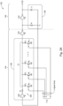
- the delay stage 128 may comprise an RC network comprising a resistor R and a capacitor C.
- Terminal ⁇ of the delay stage 128 may be connected to the resistor R and capacitor C may be connected to terminal ⁇ .
- Terminal y of the delay stage 128 may be connected to a node V X to which resistor R and capacitor C are connected.
- the delay ⁇ 1 of the RC network is generally a function of a time constant (sometimes referred to as the RC time constant) defined as R ⁇ C , which represent respective element values of resistor R and capacitor C.
- resistor R and capacitor C may be fixed-value elements. Accordingly, the delay stage 128 may provide a fixed delay.
- FIG. 2 shows additional details for delay stage 126 of the first delay section 104 in accordance with some embodiments of the present disclosure.
- the delay stage 126 may comprise a high input impedance non-inverting input buffer 202 and a variable RC network 204.
- the supply (not shown) for input buffer 202 may be the V DD supply provided to the delay stage 126, as illustrated in FIG. 1A for example.
- capacitive elements Cx may be realized using any semiconductor technology suitable for a given application of the oscillator circuit 102.
- capacitive elements Cx may be PN junction capacitors, MOSFET gate capacitors, metal-insulator-metal (MIM) capacitors, metal-oxide-metal (MOM) capacitors, and so on.
- the capacitive elements Cx may be based on the same semiconductor technology, or they may be based on different technologies.
- each of the capacitive elements Cx may have the same capacitance. In other embodiments, the capacitive elements Cx may have different capacitances.
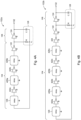
- resistor R 1 may be a fixed value element such as shown in FIG. 2A . In other embodiments (not shown), resistor R 1 may be a variable resistor and capacitor C 1 may be a fixed value element. In still other embodiments, resistor R 1 may be a variable resistor and capacitor C 1 may be a variable capacitor.
- the capacitive elements C y may be selectively switched to ground potential via a set of corresponding switches M 0 - M m-1 .
- the switches M 0 - M m-1 may be any suitable switching device.
- the switches M 0 - M m-1 may be semiconductor switches such as PNP transistors shown in FIG. 3A , for example.
- all the switches M 0 - M m-1 may be based on the same technology, or may they may be based on different technologies.
- Each of the m signal lines that comprise the selector input 312 may be connected to a respective one of the switches M 0 - M m-1 .
- the input to selector input 312 may be generated by digital logic or other suitable circuitry associated with the oscillator circuit 102 or with electronic circuit 10 ( FIG. 1A ).
- resistor R 2 may be a fixed value element such as shown in FIG. 3A . In other embodiments (not shown), resistor R 2 may be a variable resistor and capacitor C 2 may be a fixed value element. In still other embodiments (not shown), resistor R 2 may be a variable resistor and capacitor C 2 may be a variable capacitor.
- the selector inputs 112, 312 of respective delay stages 126, 326 may receive the same selection input; e.g., the same n-bit code may be provided to each selector input 112, 312. In other embodiments, each selector input 112, 312 may receive different selection inputs.
- the frequency of oscillation in oscillator circuit 102 may be controlled according to the delays ⁇ 1 , ⁇ 2 , and ⁇ 3 .
- the delay ⁇ 1 in delay stage 128 may be fixed for resistor R and capacitor C.
- the delay ⁇ 2 of the delay stage 126 may be set by asserting appropriate bit lines that comprise selector input 112 for the delay stage 126.
- the delay ⁇ 3 in delay stage 326 may be set by asserting appropriate bit lines that comprise selector signal 312. Accordingly, the frequency of the clock signal 132 may be selected as a function of the variable delays ⁇ 2 and ⁇ 3 .
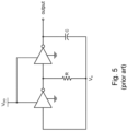
- Programmable capacitors can be difficult, since the capacitor C is a "floating" capacitor because of the behavior at node V X .
- the node V X is a floating node because the voltage at node V X may swing above and below the supply voltage in one half of a cycle of the output and above and below ground potential in the other half of the cycle.
- Programmable capacitors typically comprise a bank of switched capacitor elements. When the source (or drain) of a switch is connected at the node V X , the state of the switch can become forward biased during portions of the cycle and conduct when it is supposed to be in an OFF (non-conducting) state.
Landscapes
- Physics & Mathematics (AREA)
- Nonlinear Science (AREA)
- Inductance-Capacitance Distribution Constants And Capacitance-Resistance Oscillators (AREA)
- Semiconductor Integrated Circuits (AREA)
- Pulse Circuits (AREA)
Claims (9)
- Eine Oszillatorschaltung (102) mit einer programmierbaren Ausgangsfrequenz, die Folgendes aufweist:einen Schaltungsausgang (132), der konfiguriert ist zum Ausgeben eines Ausgangssignals;einen ersten Verzögerungsabschnitt (104), wobei der erste Verzögerungsabschnitt (104):ein Eingangsende und ein Ausgangsende hat,eine negative Verstärkung zwischen dem Eingangsende und dem Ausgangsende hat,einen Puffer (202) und einen erstes RC-Netzwerk (204) hat, das Folgendes aufweist: einen ersten Widerstand (R1) und einen ersten variablen Kondensator (C1), wobei ein erster ersten Anschluss des ersten variablen Kondensators (C1) mit dem Ausgangsende des ersten Verzögerungsabschnittes (104) verbunden ist, und ein zweiter Anschluss des ersten variablen Kondensators (C1) mit Masse verbunden ist, wobei der variable Kondensator (C1) des ersten RC-Netzwerks (204) eine Vielzahl von geschalteten Kondensatoren (Cx) zum Steuern einer variable Verzögerung aufweist, undkonfiguriert ist zum Vorsehen der variablen Verzögerung, die durch ein Steuersignal (112) eingestellt wird, das an den ersten Verzögerungsabschnitt (104) vorgesehen wird, wobei das Steuersignal (112) konfiguriert ist zum selektiven Einstellen jedes der Vielzahl von Schaltkondensatoren (Cx) auf einen AN-Zustand oder einen AUS-Zustand; undeinen zweiten Verzögerungsabschnitt (106), der elektrisch in Reihe zwischen dem ersten Verzögerungsabschnitt (104) und dem Schaltungsausgang (132) verbunden bzw. angeschlossen ist, wobei der zweite Verzögerungsabschnitt (106):ein Eingangsende und ein Ausgangsende hat,eine negative Verstärkung zwischen dem Eingangsende und dem Ausgangsende hat,konfiguriert ist zum Vorsehen einer festgelegten bzw. fixen Verzögerung, undein RC-Netzwerk (128) aufweist, das eine Widerstandskomponente bzw. resistive Komponente (R) mit fixem Wert und eine Kondensatorkomponente bzw. kapazitive Komponente (C) mit fixem Wert aufweist, wobei die Widerstandskomponente (R) mit fixem Wert einen ersten Anschluss hat, der an dem Eingangsende des zweiten Verzögerungsabschnittes (106) angeschlossen ist, und die Kondensatorkomponente (C) mit fixem Wert einen ersten Anschluss hat, der an dem Ausgangsende des zweiten Verzögerungsabschnittes (106) angeschlossen ist, und wobei der zweite Anschluss der Widerstandskomponente (R) mit fixem Wert und der zweite Anschluss der Kondensatorkomponente (C) mit fixem Wert miteinander an dem Eingang des Puffers (202) des ersten Verzögerungsabschnittes (104) angeschlossen sind;wobei das Ausgangssignal eine Frequenz hat, die eine Funktion der variablen Verzögerung aufgrund des ersten Verzögerungsabschnittes (104) und der Verzögerung aufgrund des zweiten Verzögerungsabschnittes (106) ist.
- Oszillatorschaltung (102) nach Anspruch 1, wobei der erste Verzögerungsabschnitt (104) Folgendes aufweist:ein zweites RC-Netzwerk (304), das in Reihe mit dem ersten RC-Netzwerk (204) verbunden ist und einen zweiten Widerstand (R2) und einen zweiten variablen Kondensator (C2) aufweist;wobei die variable Verzögerung des ersten Verzögerungsabschnittes (104) bestimmt wird basierend auf Kapazitäten der variablen Kondensatoren (C1, C2) der ersten und zweiten RC-Netzwerke (204, 304).
- Oszillatorschaltung (102) nach Anspruch 2,wobei das Steuersignal (112) konfiguriert ist zum Einstellen der Kapazität des variablen Kondensators (C1) des ersten RC-Netzwerks (204); undwobei ein zusätzliches Steuersignal (312) konfiguriert ist zum Einstellen der Kapazität des variablen Kondensators (C2) auf das zweite RC-Netzwerk (304).
- Oszillatorschaltung (102) nach Anspruch 1,wobei das Steuersignal (112), das an den ersten Verzögerungsabschnitt (104) vorgesehen wird, konfiguriert ist zum Einstellen einer Kapazität des variablen Kondensators (C1); undwobei die variable Verzögerung des ersten Verzögerungsabschnittes (104) bestimmt wird basierend auf der Kapazität des variablen Kondensators (C1).
- Oszillatorschaltung (102) nach Anspruch 1, wobei das Steuersignal (112) ein n-Bit-Wort ist.
- Oszillatorschaltung (102) nach Anspruch 1, wobei der erste Verzögerungsabschnitt (104) elektrisch mit dem Schaltungsausgang (132) über den zweiten Verzögerungsabschnitt (106) in einer Feedback-Schleife verbunden ist.
- Eine Oszillatorschaltung (102), die Folgendes aufweist:einen Schaltungsausgang (132), der konfiguriert ist zum Ausgeben eines Ausgangssignals;einen ersten Verzögerungsabschnitt (104), wobei der erste Verzögerungsabschnitt (104):ein Eingangsende und ein Ausgangsende hat;eine negative Verstärkung zwischen dem Eingangsende und dem Ausgangsende hat, undFolgendes aufweist:ein erstes RC-Netzwerk (204), das einen ersten Widerstand (R1) und einen ersten variablen Kondensator (C1) aufweist,einen Inverter (322), der in Reihe mit dem ersten RC-Netzwerk (204) verbunden ist,einen Puffer (202), der in Reihe mit dem ersten RC-Netzwerk (204) verbunden ist, wobei der erste Widerstand (R1) zwischen dem Ausgang des Puffers (202) und dem Eingang des Inverters (322) verbunden bzw. angeschlossen ist, wobei ein erster Anschluss des ersten variablen Kondensators (C1) mit dem Eingang des Inverters (322) verbunden ist und der zweite Anschluss des ersten variablen Kondensators (C1) mit Masse verbunden ist, undein zweites RC-Netzwerk (304), das in Reihe an einem Ausgang des Inverters (322) verbunden bzw. angeschlossen ist und einen zweiten Widerstand (R2) und einen zweiten variablen Kondensator (C2) aufweist, wobei der zweite Widerstand (R2) zwischen dem Ausgang des zweiten Inverters (322) und einem ersten Anschluss des zweiten variablen Kondensators (C2) angeschlossen ist und der zweite Anschluss des zweiten variablen Kondensators (C2) mit Masse verbunden ist,wobei die variablen Kondensatoren (C1, C2) der ersten und zweiten RC-Netzwerke (204, 304) jeweils eine Vielzahl von Schaltkondensatoren (Cx, Cy) zum Steuern einer variablen Verzögerung des ersten Verzögerungsabschnittes (104) aufweisen;wenigstens ein Steuersignal (112) an wenigstens den ersten variablen Kondensator (C1) des ersten RC-Netzwerks (204) vorgesehen wird und wenigstens ein Steuersignal (312) an wenigstens den zweiten variablen Kondensator (C2) des zweiten RC-Netzwerks (304) vorgesehen wird zum Einstellen der variablen Verzögerung des ersten Verzögerungsabschnittes (104) durch selektives Einstellen von jedem der Vielzahl von Schaltkondensatoren (Cx, Cy) auf einen AN-Zustand oder einen AUS-Zustand; undeinen zweiten Verzögerungsabschnitt (106), der elektrisch in Reihe zwischen dem ersten Verzögerungsabschnitt (104) und dem Schaltungsausgang (132) angeschlossen ist, wobei der zweite Verzögerungsabschnitt (106):ein Eingangsende und ein Ausgangsende hat,eine negative Verstärkung zwischen dem Eingangsende und dem Ausgangsende hat,eine festgelegte bzw. fixe Verzögerung hat, undein RC-Netzwerk (128) aufweist, das eine Widerstandskomponente bzw. resistive Komponente (R) mit fixem Wert und eine Kondensatorkomponente bzw. kapazitive Komponente (C) mit fixem Wert aufweist, wobei die Widerstandskomponente (R) mit fixem Wert einen ersten Anschluss hat, der an dem Eingangsende des zweiten Verzögerungsabschnittes (106) angeschlossen ist, und die Kondensatorkomponente (C) mit fixem Wert einen ersten Anschluss hat, der an dem Ausgangsende des zweiten Verzögerungsabschnittes (106) angeschlossen ist, und wobei der zweite Anschluss der resistiven Komponente (R) mit fixem Wert und der zweite Anschluss der kapazitiven Komponente (C) mit fixem Wert miteinander an den Eingang des Puffers (202) des ersten Verzögerungsabschnittes (104) angeschlossen sind;wobei das Ausgangssignal eine Frequenz hat, die eine Funktion der variablen Verzögerung aufgrund des ersten Verzögerungsabschnittes (104) und der Verzögerung aufgrund des zweiten Verzögerungsabschnittes (106) ist; undwobei der Schaltungsausgang (132) das Ausgangsende des zweiten Verzögerungsabschnittes (106) aufweist.
- Oszillatorschaltung (102) nach Anspruch 7, wobei der erste Verzögerungsabschnitt (104) weiter wenigstens ein drittes RC-Netzwerk (426b) aufweist, das in Reihe mit dem zweiten RC-Netzwerk (426a) verbunden ist und einen dritten Widerstand und einen dritten variablen Kondensator aufweist.
- Eine Schaltung, die Folgendes aufweist:eine erste Inverterstufe (122);eine zweite Inverterstufe (124) mit einem Eingang, der elektrisch an einen Ausgang der ersten Inverterstufe (324) angeschlossen ist, wobei die zweite Inverterstufe (124) einen Ausgang für ein Ausgangssignal der Oszillatorschaltung (102) gemäß einem der Ansprüche 1 bis 6 oder der Oszillatorschaltung (102) gemäß einem der Ansprüche 7 bis 8 hat, wobei die erste Inverterstufe (122) einen Eingang hat, der elektrisch an einen Ausgang des ersten Verzögerungsabschnittes (104) angeschlossen ist.
Applications Claiming Priority (3)
| Application Number | Priority Date | Filing Date | Title |
|---|---|---|---|
| US201662302735P | 2016-03-02 | 2016-03-02 | |
| US15/191,350 US9755575B1 (en) | 2016-03-02 | 2016-06-23 | Variable frequency RC oscillator |
| PCT/US2017/017518 WO2017151295A1 (en) | 2016-03-02 | 2017-02-10 | A variable frequency rc oscillator |
Publications (2)
| Publication Number | Publication Date |
|---|---|
| EP3424147A1 EP3424147A1 (de) | 2019-01-09 |
| EP3424147B1 true EP3424147B1 (de) | 2024-07-10 |
Family
ID=59702466
Family Applications (1)
| Application Number | Title | Priority Date | Filing Date |
|---|---|---|---|
| EP17706649.5A Active EP3424147B1 (de) | 2016-03-02 | 2017-02-10 | Variabler rc oszillator |
Country Status (6)
| Country | Link |
|---|---|
| US (1) | US9755575B1 (de) |
| EP (1) | EP3424147B1 (de) |
| JP (1) | JP2019511168A (de) |
| KR (1) | KR20180118137A (de) |
| CN (1) | CN108781070B (de) |
| WO (1) | WO2017151295A1 (de) |
Families Citing this family (4)
| Publication number | Priority date | Publication date | Assignee | Title |
|---|---|---|---|---|
| US10873325B2 (en) * | 2018-10-12 | 2020-12-22 | Texas Instruments Incorporated | Robust noise immune, low-skew, pulse width retainable glitch-filter |
| TWI675280B (zh) * | 2018-10-25 | 2019-10-21 | 新唐科技股份有限公司 | 時脈產生電路及其時脈調整方法 |
| GB2583353B (en) | 2019-04-24 | 2023-04-12 | Pragmatic Printing Ltd | An oscillator with improved frequency stability |
| US11811364B2 (en) | 2021-06-22 | 2023-11-07 | Samsung Electronics Co., Ltd. | Clock integrated circuit including heterogeneous oscillators and apparatus including the clock integrated circuit |
Citations (3)
| Publication number | Priority date | Publication date | Assignee | Title |
|---|---|---|---|---|
| US4316158A (en) * | 1979-01-17 | 1982-02-16 | Nippon Soken, Inc. | R-C Oscillators using plural inverters |
| US20020149087A1 (en) * | 2001-03-13 | 2002-10-17 | Fujitsu Limited | Semiconductor filter system and signal frequency control method |
| JP2006261833A (ja) * | 2005-03-15 | 2006-09-28 | Sanyo Electric Co Ltd | リング発振器 |
Family Cites Families (16)
| Publication number | Priority date | Publication date | Assignee | Title |
|---|---|---|---|---|
| JPS54181853U (de) * | 1978-06-12 | 1979-12-22 | ||
| JPS60100819A (ja) * | 1984-10-01 | 1985-06-04 | Fujitsu General Ltd | 発振回路 |
| US5519265A (en) | 1993-05-24 | 1996-05-21 | Latham, Ii; Paul W. | Adaptive RC product control in an analog-signal-manipulating circuit |
| US5552748A (en) | 1995-06-07 | 1996-09-03 | American Microsystems, Inc. | Digitally-tuned oscillator including a self-calibrating RC oscillator circuit |
| US6737926B2 (en) * | 2001-08-30 | 2004-05-18 | Micron Technology, Inc. | Method and apparatus for providing clock signals at different locations with minimal clock skew |
| DE10345236B3 (de) * | 2003-09-29 | 2005-03-10 | Infineon Technologies Ag | Verzögerungsregelkreis |
| US7245519B2 (en) | 2005-08-22 | 2007-07-17 | Freescale Semiconductor, Inc. | Digitally programmable capacitor array |
| JP2007081593A (ja) * | 2005-09-13 | 2007-03-29 | Neuro Solution Corp | 発振器、pll回路および受信機、送信機 |
| KR20070081532A (ko) * | 2006-02-13 | 2007-08-17 | 엘지전자 주식회사 | Rc 발진회로 |
| US7605668B2 (en) | 2006-12-12 | 2009-10-20 | Intel Corporation | Delay stage with controllably variable capacitive load |
| CN102006057B (zh) * | 2009-09-01 | 2013-05-08 | 杭州中科微电子有限公司 | 可编程调整起振条件的低功耗、快速起振晶体振荡器模块 |
| US8222966B2 (en) * | 2010-09-10 | 2012-07-17 | Intel Corporation | System, method and apparatus for an open loop calibrated phase wrapping phase modulator for wideband RF outphasing/polar transmitters |
| JP5807508B2 (ja) * | 2011-10-24 | 2015-11-10 | 株式会社ソシオネクスト | 発振回路を有するマイクロコントローラ |
| CN104285375B (zh) * | 2012-03-19 | 2018-07-10 | 英特尔公司 | 自偏置振荡器 |
| US9584133B2 (en) | 2012-05-31 | 2017-02-28 | Silicon Laboratories Inc. | Temperature compensated oscillator with improved noise performance |
| CN104935294B (zh) * | 2014-03-20 | 2018-07-20 | 晶宏半导体股份有限公司 | 振荡器 |
-
2016
- 2016-06-23 US US15/191,350 patent/US9755575B1/en active Active
-
2017
- 2017-02-10 JP JP2018545918A patent/JP2019511168A/ja active Pending
- 2017-02-10 KR KR1020187025097A patent/KR20180118137A/ko not_active Withdrawn
- 2017-02-10 CN CN201780014246.6A patent/CN108781070B/zh not_active Expired - Fee Related
- 2017-02-10 WO PCT/US2017/017518 patent/WO2017151295A1/en not_active Ceased
- 2017-02-10 EP EP17706649.5A patent/EP3424147B1/de active Active
Patent Citations (3)
| Publication number | Priority date | Publication date | Assignee | Title |
|---|---|---|---|---|
| US4316158A (en) * | 1979-01-17 | 1982-02-16 | Nippon Soken, Inc. | R-C Oscillators using plural inverters |
| US20020149087A1 (en) * | 2001-03-13 | 2002-10-17 | Fujitsu Limited | Semiconductor filter system and signal frequency control method |
| JP2006261833A (ja) * | 2005-03-15 | 2006-09-28 | Sanyo Electric Co Ltd | リング発振器 |
Also Published As
| Publication number | Publication date |
|---|---|
| CN108781070A (zh) | 2018-11-09 |
| WO2017151295A1 (en) | 2017-09-08 |
| JP2019511168A (ja) | 2019-04-18 |
| US9755575B1 (en) | 2017-09-05 |
| KR20180118137A (ko) | 2018-10-30 |
| US20170257065A1 (en) | 2017-09-07 |
| CN108781070B (zh) | 2022-05-17 |
| EP3424147A1 (de) | 2019-01-09 |
Similar Documents
| Publication | Publication Date | Title |
|---|---|---|
| US8222962B2 (en) | High-resolution digitally controlled oscillator and method thereof | |
| JP5229218B2 (ja) | スイッチング容量生成回路、電圧制御発振器、及びlcバンドパスフィルター | |
| KR100684050B1 (ko) | 지연회로및그것을이용한발진회로 | |
| US8031011B2 (en) | Digitally controlled oscillators | |
| EP3424147B1 (de) | Variabler rc oszillator | |
| US6486719B2 (en) | Flip-flop circuits having digital-to-time conversion latches therein | |
| US8610511B1 (en) | High-frequency digitally controlled oscillator | |
| WO2002056469A2 (en) | Ring vco based on rc timing | |
| US8466729B2 (en) | Delay cell and digitally controlled oscillator | |
| US6509803B2 (en) | Voltage-controlled oscillator having short synchronous pull-in time | |
| CN114079424A (zh) | 可控制工作周期的倍频电路及其方法 | |
| CN115149943B (zh) | 分频电路 | |
| US11942944B2 (en) | Oscillator with improved frequency stability | |
| JP3718932B2 (ja) | 中間位相クロック生成回路 | |
| US12470173B2 (en) | Oscillator apparatus and control method | |
| JP4010328B2 (ja) | 遅延回路 | |
| CN111835338A (zh) | 电平移位器装置及操作电平移位电路的方法 | |
| US6965273B2 (en) | Oscillator with improved parameters variation tolerance | |
| KR20230029512A (ko) | 2상 클록 생성 회로 | |
| JP4238931B2 (ja) | 発振回路 | |
| TW202541417A (zh) | 振盪器裝置及控制方法 | |
| JP2006060874A (ja) | 発振回路 |
Legal Events
| Date | Code | Title | Description |
|---|---|---|---|
| STAA | Information on the status of an ep patent application or granted ep patent |
Free format text: STATUS: UNKNOWN |
|
| STAA | Information on the status of an ep patent application or granted ep patent |
Free format text: STATUS: THE INTERNATIONAL PUBLICATION HAS BEEN MADE |
|
| PUAI | Public reference made under article 153(3) epc to a published international application that has entered the european phase |
Free format text: ORIGINAL CODE: 0009012 |
|
| STAA | Information on the status of an ep patent application or granted ep patent |
Free format text: STATUS: REQUEST FOR EXAMINATION WAS MADE |
|
| 17P | Request for examination filed |
Effective date: 20180802 |
|
| AK | Designated contracting states |
Kind code of ref document: A1 Designated state(s): AL AT BE BG CH CY CZ DE DK EE ES FI FR GB GR HR HU IE IS IT LI LT LU LV MC MK MT NL NO PL PT RO RS SE SI SK SM TR |
|
| AX | Request for extension of the european patent |
Extension state: BA ME |
|
| DAV | Request for validation of the european patent (deleted) | ||
| DAX | Request for extension of the european patent (deleted) | ||
| STAA | Information on the status of an ep patent application or granted ep patent |
Free format text: STATUS: EXAMINATION IS IN PROGRESS |
|
| 17Q | First examination report despatched |
Effective date: 20210224 |
|
| GRAP | Despatch of communication of intention to grant a patent |
Free format text: ORIGINAL CODE: EPIDOSNIGR1 |
|
| STAA | Information on the status of an ep patent application or granted ep patent |
Free format text: STATUS: GRANT OF PATENT IS INTENDED |
|
| INTG | Intention to grant announced |
Effective date: 20240213 |
|
| GRAS | Grant fee paid |
Free format text: ORIGINAL CODE: EPIDOSNIGR3 |
|
| GRAA | (expected) grant |
Free format text: ORIGINAL CODE: 0009210 |
|
| STAA | Information on the status of an ep patent application or granted ep patent |
Free format text: STATUS: THE PATENT HAS BEEN GRANTED |
|
| AK | Designated contracting states |
Kind code of ref document: B1 Designated state(s): AL AT BE BG CH CY CZ DE DK EE ES FI FR GB GR HR HU IE IS IT LI LT LU LV MC MK MT NL NO PL PT RO RS SE SI SK SM TR |
|
| REG | Reference to a national code |
Ref country code: CH Ref legal event code: EP |
|
| REG | Reference to a national code |
Ref country code: DE Ref legal event code: R096 Ref document number: 602017083166 Country of ref document: DE |
|
| REG | Reference to a national code |
Ref country code: LT Ref legal event code: MG9D |
|
| REG | Reference to a national code |
Ref country code: NL Ref legal event code: MP Effective date: 20240710 |
|
| PG25 | Lapsed in a contracting state [announced via postgrant information from national office to epo] |
Ref country code: PT Free format text: LAPSE BECAUSE OF FAILURE TO SUBMIT A TRANSLATION OF THE DESCRIPTION OR TO PAY THE FEE WITHIN THE PRESCRIBED TIME-LIMIT Effective date: 20241111 |
|
| REG | Reference to a national code |
Ref country code: AT Ref legal event code: MK05 Ref document number: 1702934 Country of ref document: AT Kind code of ref document: T Effective date: 20240710 |
|
| PG25 | Lapsed in a contracting state [announced via postgrant information from national office to epo] |
Ref country code: NL Free format text: LAPSE BECAUSE OF FAILURE TO SUBMIT A TRANSLATION OF THE DESCRIPTION OR TO PAY THE FEE WITHIN THE PRESCRIBED TIME-LIMIT Effective date: 20240710 |
|
| PG25 | Lapsed in a contracting state [announced via postgrant information from national office to epo] |
Ref country code: PT Free format text: LAPSE BECAUSE OF FAILURE TO SUBMIT A TRANSLATION OF THE DESCRIPTION OR TO PAY THE FEE WITHIN THE PRESCRIBED TIME-LIMIT Effective date: 20241111 Ref country code: NL Free format text: LAPSE BECAUSE OF FAILURE TO SUBMIT A TRANSLATION OF THE DESCRIPTION OR TO PAY THE FEE WITHIN THE PRESCRIBED TIME-LIMIT Effective date: 20240710 |
|
| PG25 | Lapsed in a contracting state [announced via postgrant information from national office to epo] |
Ref country code: NO Free format text: LAPSE BECAUSE OF FAILURE TO SUBMIT A TRANSLATION OF THE DESCRIPTION OR TO PAY THE FEE WITHIN THE PRESCRIBED TIME-LIMIT Effective date: 20241010 |
|
| PG25 | Lapsed in a contracting state [announced via postgrant information from national office to epo] |
Ref country code: GR Free format text: LAPSE BECAUSE OF FAILURE TO SUBMIT A TRANSLATION OF THE DESCRIPTION OR TO PAY THE FEE WITHIN THE PRESCRIBED TIME-LIMIT Effective date: 20241011 Ref country code: PL Free format text: LAPSE BECAUSE OF FAILURE TO SUBMIT A TRANSLATION OF THE DESCRIPTION OR TO PAY THE FEE WITHIN THE PRESCRIBED TIME-LIMIT Effective date: 20240710 Ref country code: FI Free format text: LAPSE BECAUSE OF FAILURE TO SUBMIT A TRANSLATION OF THE DESCRIPTION OR TO PAY THE FEE WITHIN THE PRESCRIBED TIME-LIMIT Effective date: 20240710 |
|
| PG25 | Lapsed in a contracting state [announced via postgrant information from national office to epo] |
Ref country code: BG Free format text: LAPSE BECAUSE OF FAILURE TO SUBMIT A TRANSLATION OF THE DESCRIPTION OR TO PAY THE FEE WITHIN THE PRESCRIBED TIME-LIMIT Effective date: 20240710 |
|
| PG25 | Lapsed in a contracting state [announced via postgrant information from national office to epo] |
Ref country code: LV Free format text: LAPSE BECAUSE OF FAILURE TO SUBMIT A TRANSLATION OF THE DESCRIPTION OR TO PAY THE FEE WITHIN THE PRESCRIBED TIME-LIMIT Effective date: 20240710 |
|
| PG25 | Lapsed in a contracting state [announced via postgrant information from national office to epo] |
Ref country code: IS Free format text: LAPSE BECAUSE OF FAILURE TO SUBMIT A TRANSLATION OF THE DESCRIPTION OR TO PAY THE FEE WITHIN THE PRESCRIBED TIME-LIMIT Effective date: 20241110 Ref country code: AT Free format text: LAPSE BECAUSE OF FAILURE TO SUBMIT A TRANSLATION OF THE DESCRIPTION OR TO PAY THE FEE WITHIN THE PRESCRIBED TIME-LIMIT Effective date: 20240710 |
|
| PG25 | Lapsed in a contracting state [announced via postgrant information from national office to epo] |
Ref country code: HR Free format text: LAPSE BECAUSE OF FAILURE TO SUBMIT A TRANSLATION OF THE DESCRIPTION OR TO PAY THE FEE WITHIN THE PRESCRIBED TIME-LIMIT Effective date: 20240710 |
|
| PG25 | Lapsed in a contracting state [announced via postgrant information from national office to epo] |
Ref country code: ES Free format text: LAPSE BECAUSE OF FAILURE TO SUBMIT A TRANSLATION OF THE DESCRIPTION OR TO PAY THE FEE WITHIN THE PRESCRIBED TIME-LIMIT Effective date: 20240710 Ref country code: RS Free format text: LAPSE BECAUSE OF FAILURE TO SUBMIT A TRANSLATION OF THE DESCRIPTION OR TO PAY THE FEE WITHIN THE PRESCRIBED TIME-LIMIT Effective date: 20241010 |
|
| PG25 | Lapsed in a contracting state [announced via postgrant information from national office to epo] |
Ref country code: RS Free format text: LAPSE BECAUSE OF FAILURE TO SUBMIT A TRANSLATION OF THE DESCRIPTION OR TO PAY THE FEE WITHIN THE PRESCRIBED TIME-LIMIT Effective date: 20241010 Ref country code: PL Free format text: LAPSE BECAUSE OF FAILURE TO SUBMIT A TRANSLATION OF THE DESCRIPTION OR TO PAY THE FEE WITHIN THE PRESCRIBED TIME-LIMIT Effective date: 20240710 Ref country code: NO Free format text: LAPSE BECAUSE OF FAILURE TO SUBMIT A TRANSLATION OF THE DESCRIPTION OR TO PAY THE FEE WITHIN THE PRESCRIBED TIME-LIMIT Effective date: 20241010 Ref country code: LV Free format text: LAPSE BECAUSE OF FAILURE TO SUBMIT A TRANSLATION OF THE DESCRIPTION OR TO PAY THE FEE WITHIN THE PRESCRIBED TIME-LIMIT Effective date: 20240710 Ref country code: IS Free format text: LAPSE BECAUSE OF FAILURE TO SUBMIT A TRANSLATION OF THE DESCRIPTION OR TO PAY THE FEE WITHIN THE PRESCRIBED TIME-LIMIT Effective date: 20241110 Ref country code: HR Free format text: LAPSE BECAUSE OF FAILURE TO SUBMIT A TRANSLATION OF THE DESCRIPTION OR TO PAY THE FEE WITHIN THE PRESCRIBED TIME-LIMIT Effective date: 20240710 Ref country code: GR Free format text: LAPSE BECAUSE OF FAILURE TO SUBMIT A TRANSLATION OF THE DESCRIPTION OR TO PAY THE FEE WITHIN THE PRESCRIBED TIME-LIMIT Effective date: 20241011 Ref country code: FI Free format text: LAPSE BECAUSE OF FAILURE TO SUBMIT A TRANSLATION OF THE DESCRIPTION OR TO PAY THE FEE WITHIN THE PRESCRIBED TIME-LIMIT Effective date: 20240710 Ref country code: ES Free format text: LAPSE BECAUSE OF FAILURE TO SUBMIT A TRANSLATION OF THE DESCRIPTION OR TO PAY THE FEE WITHIN THE PRESCRIBED TIME-LIMIT Effective date: 20240710 Ref country code: BG Free format text: LAPSE BECAUSE OF FAILURE TO SUBMIT A TRANSLATION OF THE DESCRIPTION OR TO PAY THE FEE WITHIN THE PRESCRIBED TIME-LIMIT Effective date: 20240710 Ref country code: AT Free format text: LAPSE BECAUSE OF FAILURE TO SUBMIT A TRANSLATION OF THE DESCRIPTION OR TO PAY THE FEE WITHIN THE PRESCRIBED TIME-LIMIT Effective date: 20240710 |
|
| PGFP | Annual fee paid to national office [announced via postgrant information from national office to epo] |
Ref country code: DE Payment date: 20250109 Year of fee payment: 9 |
|
| REG | Reference to a national code |
Ref country code: DE Ref legal event code: R097 Ref document number: 602017083166 Country of ref document: DE |
|
| PG25 | Lapsed in a contracting state [announced via postgrant information from national office to epo] |
Ref country code: RO Free format text: LAPSE BECAUSE OF FAILURE TO SUBMIT A TRANSLATION OF THE DESCRIPTION OR TO PAY THE FEE WITHIN THE PRESCRIBED TIME-LIMIT Effective date: 20240710 Ref country code: SM Free format text: LAPSE BECAUSE OF FAILURE TO SUBMIT A TRANSLATION OF THE DESCRIPTION OR TO PAY THE FEE WITHIN THE PRESCRIBED TIME-LIMIT Effective date: 20240710 Ref country code: DK Free format text: LAPSE BECAUSE OF FAILURE TO SUBMIT A TRANSLATION OF THE DESCRIPTION OR TO PAY THE FEE WITHIN THE PRESCRIBED TIME-LIMIT Effective date: 20240710 |
|
| PG25 | Lapsed in a contracting state [announced via postgrant information from national office to epo] |
Ref country code: EE Free format text: LAPSE BECAUSE OF FAILURE TO SUBMIT A TRANSLATION OF THE DESCRIPTION OR TO PAY THE FEE WITHIN THE PRESCRIBED TIME-LIMIT Effective date: 20240710 |
|
| PG25 | Lapsed in a contracting state [announced via postgrant information from national office to epo] |
Ref country code: CZ Free format text: LAPSE BECAUSE OF FAILURE TO SUBMIT A TRANSLATION OF THE DESCRIPTION OR TO PAY THE FEE WITHIN THE PRESCRIBED TIME-LIMIT Effective date: 20240710 |
|
| PGFP | Annual fee paid to national office [announced via postgrant information from national office to epo] |
Ref country code: FR Payment date: 20250110 Year of fee payment: 9 |
|
| PG25 | Lapsed in a contracting state [announced via postgrant information from national office to epo] |
Ref country code: SK Free format text: LAPSE BECAUSE OF FAILURE TO SUBMIT A TRANSLATION OF THE DESCRIPTION OR TO PAY THE FEE WITHIN THE PRESCRIBED TIME-LIMIT Effective date: 20240710 Ref country code: IT Free format text: LAPSE BECAUSE OF FAILURE TO SUBMIT A TRANSLATION OF THE DESCRIPTION OR TO PAY THE FEE WITHIN THE PRESCRIBED TIME-LIMIT Effective date: 20240710 |
|
| PGFP | Annual fee paid to national office [announced via postgrant information from national office to epo] |
Ref country code: GB Payment date: 20250109 Year of fee payment: 9 |
|
| PLBE | No opposition filed within time limit |
Free format text: ORIGINAL CODE: 0009261 |
|
| STAA | Information on the status of an ep patent application or granted ep patent |
Free format text: STATUS: NO OPPOSITION FILED WITHIN TIME LIMIT |
|
| 26N | No opposition filed |
Effective date: 20250411 |
|
| PG25 | Lapsed in a contracting state [announced via postgrant information from national office to epo] |
Ref country code: SE Free format text: LAPSE BECAUSE OF FAILURE TO SUBMIT A TRANSLATION OF THE DESCRIPTION OR TO PAY THE FEE WITHIN THE PRESCRIBED TIME-LIMIT Effective date: 20240710 |
|
| PG25 | Lapsed in a contracting state [announced via postgrant information from national office to epo] |
Ref country code: MC Free format text: LAPSE BECAUSE OF FAILURE TO SUBMIT A TRANSLATION OF THE DESCRIPTION OR TO PAY THE FEE WITHIN THE PRESCRIBED TIME-LIMIT Effective date: 20240710 |
|
| REG | Reference to a national code |
Ref country code: CH Ref legal event code: PL |
|
| PG25 | Lapsed in a contracting state [announced via postgrant information from national office to epo] |
Ref country code: LU Free format text: LAPSE BECAUSE OF NON-PAYMENT OF DUE FEES Effective date: 20250210 |
|
| PG25 | Lapsed in a contracting state [announced via postgrant information from national office to epo] |
Ref country code: CH Free format text: LAPSE BECAUSE OF NON-PAYMENT OF DUE FEES Effective date: 20250228 |