EP3422546A1 - Transistor driving circuit - Google Patents
Transistor driving circuit Download PDFInfo
- Publication number
- EP3422546A1 EP3422546A1 EP17755827.7A EP17755827A EP3422546A1 EP 3422546 A1 EP3422546 A1 EP 3422546A1 EP 17755827 A EP17755827 A EP 17755827A EP 3422546 A1 EP3422546 A1 EP 3422546A1
- Authority
- EP
- European Patent Office
- Prior art keywords
- power supply
- voltage power
- circuit
- voltage
- low
- Prior art date
- Legal status (The legal status is an assumption and is not a legal conclusion. Google has not performed a legal analysis and makes no representation as to the accuracy of the status listed.)
- Granted
Links
- 238000001514 detection method Methods 0.000 claims abstract description 25
- 230000005611 electricity Effects 0.000 claims abstract description 14
- 230000000087 stabilizing effect Effects 0.000 claims description 24
- 230000001681 protective effect Effects 0.000 claims description 8
- 238000010586 diagram Methods 0.000 description 9
- 230000003068 static effect Effects 0.000 description 6
- 230000001808 coupling effect Effects 0.000 description 4
- 238000005516 engineering process Methods 0.000 description 3
- 230000001960 triggered effect Effects 0.000 description 3
- 230000008901 benefit Effects 0.000 description 2
- 230000005540 biological transmission Effects 0.000 description 1
- 230000008859 change Effects 0.000 description 1
- 230000003247 decreasing effect Effects 0.000 description 1
- 230000000694 effects Effects 0.000 description 1
- 230000005669 field effect Effects 0.000 description 1
- 238000002955 isolation Methods 0.000 description 1
- 239000000463 material Substances 0.000 description 1
- 230000004048 modification Effects 0.000 description 1
- 238000012986 modification Methods 0.000 description 1
- 239000004065 semiconductor Substances 0.000 description 1
Images


Classifications
-
- H—ELECTRICITY
- H03—ELECTRONIC CIRCUITRY
- H03K—PULSE TECHNIQUE
- H03K17/00—Electronic switching or gating, i.e. not by contact-making and –breaking
- H03K17/08—Modifications for protecting switching circuit against overcurrent or overvoltage
- H03K17/081—Modifications for protecting switching circuit against overcurrent or overvoltage without feedback from the output circuit to the control circuit
- H03K17/08104—Modifications for protecting switching circuit against overcurrent or overvoltage without feedback from the output circuit to the control circuit in field-effect transistor switches
-
- H—ELECTRICITY
- H02—GENERATION; CONVERSION OR DISTRIBUTION OF ELECTRIC POWER
- H02H—EMERGENCY PROTECTIVE CIRCUIT ARRANGEMENTS
- H02H9/00—Emergency protective circuit arrangements for limiting excess current or voltage without disconnection
- H02H9/04—Emergency protective circuit arrangements for limiting excess current or voltage without disconnection responsive to excess voltage
- H02H9/045—Emergency protective circuit arrangements for limiting excess current or voltage without disconnection responsive to excess voltage adapted to a particular application and not provided for elsewhere
-
- H—ELECTRICITY
- H01—ELECTRIC ELEMENTS
- H01L—SEMICONDUCTOR DEVICES NOT COVERED BY CLASS H10
- H01L27/00—Devices consisting of a plurality of semiconductor or other solid-state components formed in or on a common substrate
- H01L27/02—Devices consisting of a plurality of semiconductor or other solid-state components formed in or on a common substrate including semiconductor components specially adapted for rectifying, oscillating, amplifying or switching and having potential barriers; including integrated passive circuit elements having potential barriers
- H01L27/0203—Particular design considerations for integrated circuits
- H01L27/0248—Particular design considerations for integrated circuits for electrical or thermal protection, e.g. electrostatic discharge [ESD] protection
- H01L27/0251—Particular design considerations for integrated circuits for electrical or thermal protection, e.g. electrostatic discharge [ESD] protection for MOS devices
- H01L27/0255—Particular design considerations for integrated circuits for electrical or thermal protection, e.g. electrostatic discharge [ESD] protection for MOS devices using diodes as protective elements
-
- H—ELECTRICITY
- H02—GENERATION; CONVERSION OR DISTRIBUTION OF ELECTRIC POWER
- H02M—APPARATUS FOR CONVERSION BETWEEN AC AND AC, BETWEEN AC AND DC, OR BETWEEN DC AND DC, AND FOR USE WITH MAINS OR SIMILAR POWER SUPPLY SYSTEMS; CONVERSION OF DC OR AC INPUT POWER INTO SURGE OUTPUT POWER; CONTROL OR REGULATION THEREOF
- H02M1/00—Details of apparatus for conversion
- H02M1/08—Circuits specially adapted for the generation of control voltages for semiconductor devices incorporated in static converters
-
- H—ELECTRICITY
- H03—ELECTRONIC CIRCUITRY
- H03K—PULSE TECHNIQUE
- H03K17/00—Electronic switching or gating, i.e. not by contact-making and –breaking
- H03K17/08—Modifications for protecting switching circuit against overcurrent or overvoltage
- H03K17/081—Modifications for protecting switching circuit against overcurrent or overvoltage without feedback from the output circuit to the control circuit
- H03K17/0814—Modifications for protecting switching circuit against overcurrent or overvoltage without feedback from the output circuit to the control circuit by measures taken in the output circuit
- H03K17/08142—Modifications for protecting switching circuit against overcurrent or overvoltage without feedback from the output circuit to the control circuit by measures taken in the output circuit in field-effect transistor switches
-
- H—ELECTRICITY
- H03—ELECTRONIC CIRCUITRY
- H03K—PULSE TECHNIQUE
- H03K17/00—Electronic switching or gating, i.e. not by contact-making and –breaking
- H03K17/08—Modifications for protecting switching circuit against overcurrent or overvoltage
- H03K17/082—Modifications for protecting switching circuit against overcurrent or overvoltage by feedback from the output to the control circuit
- H03K17/0822—Modifications for protecting switching circuit against overcurrent or overvoltage by feedback from the output to the control circuit in field-effect transistor switches
-
- H—ELECTRICITY
- H03—ELECTRONIC CIRCUITRY
- H03K—PULSE TECHNIQUE
- H03K17/00—Electronic switching or gating, i.e. not by contact-making and –breaking
- H03K17/16—Modifications for eliminating interference voltages or currents
- H03K17/161—Modifications for eliminating interference voltages or currents in field-effect transistor switches
- H03K17/162—Modifications for eliminating interference voltages or currents in field-effect transistor switches without feedback from the output circuit to the control circuit
- H03K17/163—Soft switching
-
- H—ELECTRICITY
- H03—ELECTRONIC CIRCUITRY
- H03K—PULSE TECHNIQUE
- H03K17/00—Electronic switching or gating, i.e. not by contact-making and –breaking
- H03K17/16—Modifications for eliminating interference voltages or currents
- H03K17/161—Modifications for eliminating interference voltages or currents in field-effect transistor switches
- H03K17/165—Modifications for eliminating interference voltages or currents in field-effect transistor switches by feedback from the output circuit to the control circuit
- H03K17/166—Soft switching
-
- H—ELECTRICITY
- H03—ELECTRONIC CIRCUITRY
- H03K—PULSE TECHNIQUE
- H03K19/00—Logic circuits, i.e. having at least two inputs acting on one output; Inverting circuits
- H03K19/0175—Coupling arrangements; Interface arrangements
- H03K19/0185—Coupling arrangements; Interface arrangements using field effect transistors only
Definitions
- This application relates to the field of drive circuit technologies, and in particular, to a drive circuit of a transistor.
- a high-voltage transistor drive chip is mainly used to drive a power device such as a MOSFET (Metal-Oxide-Semiconductor Field-Effect Transistor) or an IGBT (Insulated Gate Bipolar Transistor), and is generally applied to fields such as industries and household appliance inverters.
- a power device such as a MOSFET (Metal-Oxide-Semiconductor Field-Effect Transistor) or an IGBT (Insulated Gate Bipolar Transistor)
- the high-voltage transistor drive chip has a high-voltage power supply domain and a low-voltage power supply domain, static electricity between the power supply domains needs to be discharged by using a high-voltage device.
- an ESD Electrostatic Discharge
- the chip includes two power supply domains: a low-voltage power supply domain (VCC is a low-voltage power supply and VSS is a low-voltage ground) and a high-voltage power supply domain (VB is a high-voltage power supply and VS is a high-voltage ground).
- the two power supply domains are connected together by using a level-shifter circuit (level shifter, and inside of FIG. 7 includes a level-shifter 1 and a level-shifter 2 that are independent and in a same structure) and a high-voltage ESD device.
- a level-shifter circuit level shifter, and inside of FIG. 7 includes a level-shifter 1 and a level-shifter 2 that are independent and in a same structure
- a high-voltage ESD device Inside of an independent power supply domain, and power supply grounded VB-VS and VCC-VSS include independent ESD devices (which are commonly a diode, a triode, a CMOS tube, and the like), used to perform
- the level-shifter mainly includes: a DMOS (M1 and M2 in FIG. 7 ), a DMOS source device (a source is grounded in FIG. 7 ), and a DMOS drain detection circuit (formed by detection resistors R1 and R2 and voltage stabilizing tubes Z1 and Z2 in FIG. 7 ). Voltages on the detection resistors R1 and R2 are changed by controlling on and off of the DMOS-M1 and the DMOS-M2, to shift a low-voltage signal to a high-voltage signal.
- This application is aimed to at least resolve one of the technical problems in the related technology to some extent.
- the objective of this application is to provide a drive circuit of a transistor.
- the drive circuit of the transistor has an advantage of a strong anti-static electricity capability, thereby further improving the stability and the reliability of the drive circuit of the transistor.
- a drive circuit of a transistor including: a high-voltage power supply and a low-voltage power supply; a circuit in a high-voltage power supply domain and a circuit in a low-voltage power supply domain, where the circuit in a high-voltage power supply domain is connected to the high-voltage power supply, and the circuit in a low-voltage power supply domain is connected to the low-voltage power supply; an electrostatic discharge apparatus, where the electrostatic discharge apparatus is separately disposed between electrodes of the high-voltage power supply, between electrodes of the low-voltage power supply, and between a positive electrode of the high-voltage power supply and a negative electrode of the low-voltage power supply; a level shifter circuit, where the level shifter circuit includes a level detection circuit, a current limiting module, a discharge module, and a switch tube, where the level detection circuit is connected to the positive electrode of the high-voltage power supply and is separately connected to the current limiting module,
- a current limiting module is added in a level shifter circuit, to increase the internal resistance of a path on which electrostatic discharge is performed by using the level shifter circuit, so that when the electrostatic discharge is performed, the current on the path is limited, which prevents the level shifter circuit from being damaged.
- the voltage reaches a trigger voltage of an electrostatic discharge apparatus (such as a high-voltage ESD device)
- the electrostatic discharge apparatus is started, to discharge a large part of energy, to further protect the drive circuit of the transistor.
- a discharge module is increased in the level shifter circuit, to provide a low-resistance path from a negative electrode of a high-voltage power supply to a drain of a switch tube.
- an electrostatic discharge path is increased to shunt the electrostatic discharge, and the discharge module may restrain the potential of a level detection circuit, to prevent the potential from being lower than the voltage of the negative electrode of the high-voltage power supply.
- the drive circuit of the transistor has a strong anti-static electricity capability, thereby further improving the stability and the reliability of the drive circuit of the transistor.
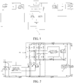
- FIG. 1 is structural block diagram of a drive circuit of a transistor according to an embodiment of this application.
- FIG. 2 is a circuit diagram of a drive circuit of a transistor according to an embodiment of this application.
- a drive circuit 100 of a transistor according to an embodiment of this application includes: a high-voltage power supply 110, a low-voltage power supply 120, a circuit in a high-voltage power supply domain 130, a circuit in a low-voltage power supply domain 140, an electrostatic discharge apparatus 150, and a level shifter circuit 160.
- high-voltage and low-voltage in the high-voltage power supply and the low-voltage power supply are used to represent two power supplies with different voltages.
- high-voltage and low-voltage in the circuit in a high-voltage power supply domain and the circuit in a low-voltage power supply domain are used to represent two power supply domain circuits with different voltages.
- the voltage of the high-voltage power supply may be 20 V
- the voltage of the low-voltage power supply may be 10 V
- the voltage of the circuit in a high-voltage power supply domain may be 20 V
- the voltage of the circuit in a low-voltage power supply domain may be 10 V
- the voltage of the high-voltage power supply may be 10 V
- the voltage of the low-voltage power supply may be 7 V
- the voltage of the circuit in a high-voltage power supply domain may be 10 V
- the voltage of the circuit in a low-voltage power supply domain may be 7 V.
- the circuit in a high-voltage power supply domain 130 is connected to the high-voltage power supply 110, and the circuit in a low-voltage power supply domain 140 is connected to the low-voltage power supply 120.
- the electrostatic discharge apparatus 150 is separately disposed between electrodes of the high-voltage power supply 110 (that is: between a positive electrode VB and a negative electrode VS), between electrodes of the low-voltage power supply 120 (that is: between a positive electrode VCC and a negative electrode VSS), and between the positive electrode VB of the high-voltage power supply 110 and the negative electrode VSS of the low-voltage power supply 120.
- the level shifter circuit 160 includes a level detection circuit 161, a current limiting module 162, a discharge module 163, and a switch tube 164.
- a first end of the level detection circuit 161 is connected to the positive electrode VB of the high-voltage power supply 110 and a second end of the level detection circuit 161 is separately connected to a first end of the current limiting module 162, a first end of the discharge module 163, and the circuit in a high-voltage power supply domain 130, a second end of the current limiting module 162 is connected to a first end of the switch tube 164, a second end of the discharge module 163 is connected to the negative electrode VS of the high-voltage power supply 110, a control end of the switch tube 164 is connected to the circuit in a low-voltage power supply domain 140 and a second end of the switch tube 164 is connected to the negative electrode VSS of the low-voltage power supply 120, the current limiting module 162 is configured to limit the discharged electricity when the drive circuit performs electrostatic discharge, and the discharge module 163 is configured to form a discharge assisting path between the negative electrode VS of the high-voltage power supply 110 and the first
- the level detection circuit 161 includes a voltage stabilizing tube Z1 and a first resistor R1, a cathode of the voltage stabilizing tube Z1 is connected to the positive electrode VB of the high-voltage power supply 110, an anode of the voltage stabilizing tube Z1 is connected to the circuit in a high-voltage power supply domain 130 (that is: the anode of the voltage stabilizing tube Z1 is connected to the circuit in a high-voltage power supply domain 130 by using a detection point A1), and the first resistor R1 is connected to the voltage stabilizing tube Z1 in parallel.
- the current limiting module 162 includes a current limiting resistor R3, one end of the current limiting resistor R3 is connected to the anode of the voltage stabilizing tube Z1, and the other end of the current limiting resistor R3 is connected to the first end of the switch tube 164.
- the discharge module 163 includes a first diode D3, a cathode of the first diode D3 is connected to the anode of the voltage stabilizing tube Z1, and an anode of the first diode D3 is connected to the negative electrode VS of the high-voltage power supply 110.
- the switch tube 164 is a second MOS tube M1. Further, the control end of the switch tube 164 is a gate G of the second MOS tube M1, the first end is a drain D of the second MOS tube M1, and the second end is a source S of the second MOS tube M1.
- the electrostatic discharge apparatus 150 includes: a third electrostatic discharge device 151, a fourth electrostatic discharge device 152, and a fifth electrostatic discharge device 153.
- the third electrostatic discharge device 151 and the fourth electrostatic discharge device 152 are ESD devices.
- the fifth electrostatic discharge device 153 is a high-voltage ESD device (High Voltage Isolation Junction) shown in FIG. 2 .
- the third electrostatic discharge device 151 is an ESD device disposed between electrodes of the high-voltage power supply 110, that is, disposed between the positive electrode VB and the negative electrode VS of the high-voltage power supply 110.
- the fourth electrostatic discharge device 152 is an ESD device disposed between electrodes of the low-voltage power supply 110, that is, disposed between the positive electrode VCC and the negative electrode VSS of the low-voltage power supply 120.
- the fifth electrostatic discharge device 153 is a high-voltage ESD device 153 disposed between the positive electrode VB of the high-voltage power supply 110 and the negative electrode VSS of the low-voltage power supply 120, that is, disposed between the positive electrode VB of the high-voltage power supply 110 and the negative electrode VSS of the low-voltage power supply 120.
- FIG. 2 shows a drive circuit 100 of a transistor including two level shifter circuits 160 that are connected in parallel and in a same structure.
- the other level shifter circuit 160 is formed by a voltage stabilizing tube Z2, a resistor R2, a resistor R4, a diode D4, and a MOS tube M2. Details are not provided herein again.
- the circuit in a high-voltage power supply domain 130 is connected to the circuit in a low-voltage power supply domain 140 by using the level shifter circuit 160, and the circuit in a high-voltage power supply domain 130 is connected to the circuit in a low-voltage power supply domain 140 by using a high-voltage ESD device.
- the level shifter circuit 160 mainly performs level shifting, to shift a signal in a low-voltage region to a high-voltage region, to implement transmission of the signal.
- FIG. 2 includes two level shifter circuits 160 connected in parallel.
- a gate signal of a high-voltage device DMOS Double-Diffused MOSFET
- a source of the second MOS tube M1 is connected to the negative electrode VSS of the low-voltage power supply 120
- a drain of the second MOS tube M1 is connected to one end of the resistor R3, the other end of the resistor R3 is connected to the anode of the voltage stabilizing tube Z1, the cathode of the voltage stabilizing tube Z1 is connected to the positive electrode VB of the high-voltage power supply 110
- the first resistor R1 is connected to the voltage stabilizing tube Z1 in parallel
- the anode of the voltage stabilizing tube Z1 is a detection point A1
- an electric signal of the detection point A1 is used as an input signal of the circuit in a high-voltage power supply domain 130
- the cathode of the first diode D3 is connected to the
- a gate signal of a high-voltage device DMOS, that is, a MOS tube M2, of the other level shifter circuit 160 is generated by the circuit in a low-voltage power supply domain 140, a source of the MOS tube M2 is connected to the negative electrode VSS of the low-voltage power supply 120, a drain of the MOS tube M2 is connected to one end of the resistor R4, the other end of the resistor R4 is connected to the anode of the voltage stabilizing tube Z2, the cathode of the voltage stabilizing tube Z2 is connected to the positive electrode VB of the high-voltage power supply 110, the resistor R2 is connected to the voltage stabilizing tube Z2 in parallel, the anode of the voltage stabilizing tube Z2 is a detection point A2, an electric signal of the detection point A2 is used as an input signal of the circuit in a high-voltage power supply domain 130, a cathode of the diode D4 is connected to the detection point A2, and an anode of the diode D4
- a changed voltage signal may be generated on the first resistor R1 connected to the drain of the second MOS tube M1, and input to the circuit in a high-voltage power supply domain 130 for processing, thereby implementing shifting from a low-voltage signal to a high-voltage signal.
- the first diode D3 provides a low-resistance path from the negative electrode VS of the high-voltage power supply 110 to the drain of the second MOS tube M1.
- a discharge path from the negative electrode VS of the high-voltage power supply 110 to the low-voltage power supply domain not only includes: the discharge path VS ⁇ VB ⁇ DMOS/high-voltage ESD device ⁇ VSS ⁇ VCC, but also includes the discharge assisting path VS ⁇ DMOS ⁇ VSS ⁇ VCC. This helps to shunt the ESD. Meanwhile, the first diode D3 may restrain the potential of the detection point A1, to prevent the potential of the detection point A1 from being lower than the voltage of the negative electrode VS of the high-voltage power supply 110.
- the voltage stabilizing tube Z1 is connected to the first resistor R1 in parallel, and may restrain the voltages at two ends of the resistor, to prevent the voltages from exceeding the power supply range of the high-voltage power supply domain and damaging the chip.
- the current limiting resistor R3 may limit the current of the path of the high-voltage device DMOS when performing electrostatic discharge, so that the second MOS tube M1 of the high-voltage device DMOS cannot be easily damaged.
- some voltages may be superposed on the drain of the second MOS tube M1, so that when the voltage of the positive electrode VB of the high-voltage power supply 110 reaches a trigger voltage of the high-voltage ESD device 153, the high-voltage ESD device 153 is triggered, and a large part of static electricity may be discharged by using the high-voltage ESD device 153, to protect the drive circuit 100 of the transistor.
- the other level shifter circuit is similar, and details are not described herein.
- the high-voltage ESD device 153 is between the positive electrode VB of the high-voltage power supply 110 and the negative electrode VSS of the low-voltage power supply 120, and similar to a reversed high-voltage diode, and has a higher withstand voltage and a strong over-current capability.
- the high-voltage ESD device 153 needs to be triggered as much as possible. This helps to discharge the static electricity, and protect the drive circuit 100 of the transistor.
- the second MOS tube M1 of the high-voltage device DMOS is preferentially started due to a coupling effect.
- the current limiting resistor R3 When the current flows through the first resistor R1, the current limiting resistor R3 generates a voltage, and when a drain voltage of the second MOS tube M1 and the sum of voltages on the first resistor R1 and the current limiting resistor R3 reach the trigger voltage of the high-voltage ESD device 153, the high-voltage ESD device 153 is triggered, to discharge a large part of energy.
- discharge paths of the second MOS tube M1 and the high-voltage ESD device 153 take effect at the same time, the second MOS tube M1 discharges a small part of energy, and the high-voltage ESD device 153 discharges a large part of energy. That is, when electrostatic discharge is performed, the path is discharged as a secondary electrostatic discharge path by using the high-voltage device DMOS of the level shifter circuit 160, and discharged as a main electrostatic discharge path by using the high-voltage ESD device 153.
- the two discharge manners act together, which greatly improves the high voltage, and further greatly improves an electrostatic discharge capability of the drive circuit 100 of the transistor.
- the other level shifter circuit is similar, and details are not described herein.
- a current limiting module is added in a level shifter circuit, to increase the internal resistance of a path on which electrostatic discharge is performed by using the level shifter circuit, so that when the electrostatic discharge is performed, the current on the path is limited, which prevents the level shifter circuit from being damaged.
- the voltage reaches a trigger voltage of an electrostatic discharge apparatus (such as a high-voltage ESD device)
- the electrostatic discharge apparatus is started, to discharge a large part of energy, to further protect the drive circuit of the transistor.
- a discharge module is increased in the level shifter circuit, to provide a low-resistance path from a negative electrode of a high-voltage power supply to a drain of a switch tube.
- an electrostatic discharge path is increased to shunt the electrostatic discharge, and the discharge module may restrain the potential of a level detection circuit, to prevent the potential from being lower than the voltage of the negative electrode of the high-voltage power supply.
- the drive circuit of the transistor has a strong anti-static electricity capability, thereby further improving the stability and the reliability of the drive circuit of the transistor.
- the drive circuit 100 of the transistor further includes: a protective circuit 165 (that is: a device and an ESD device), and the protective circuit 170 is disposed between the second end of the switch tube 164 and the negative electrode VSS of the low-voltage power supply 120. That is: a source of the high-voltage device DMOS is connected to the negative electrode VSS of the low-voltage power supply 120 by using the device, and the ESD device is connected to the device in parallel.
- the source of the second MOS tube M1 is further connected to the negative electrode VSS of the low-voltage power supply 120 by connecting to the device and the ESD device connected to the device in parallel.
- a path of the high-voltage device DMOS is preferentially started due to a coupling effect. Because the source of the second MOS tube M1 of the high-voltage device DMOS is connected to the device, the source has a higher voltage. When the voltage exceeds a trigger voltage of the ESD device connected to the device in parallel, the ESD device is started, and ESD energy is rapidly discharged to the negative electrode VSS of the low-voltage power supply 120, to prevent the high-voltage device DMOS and the device from being damaged, and also increase an over ESD current capability of the path of the high-voltage device DMOS.
- the protective circuit includes: a second resistor and a first electrostatic discharge device, such as a second resistor R5 and an ESD device, or a second resistor R6 and an ESD device.
- the second resistor R5 and the ESD device are used as an example.
- the second resistor R5 is connected to the ESD device in parallel, one end of the second resistor R5 is connected to the second end of the switch tube 164, and the other end of the second resistor R5 is connected to the negative electrode VSS of the low-voltage power supply 120.
- the first electrostatic discharge device is connected to the second resistor R5 in parallel.
- a gate signal of the high-voltage device DMOS is generated by the circuit in a low-voltage power supply domain 140, the source is further connected to the negative electrode VSS of the low-voltage power supply 120 by connecting to the resistor R5 and the ESD device connected to the resistor in parallel, and the second resistor R5 is connected to the ESD device in parallel.
- the electrostatic discharge is performed from the high-voltage power supply domain to the low-voltage power supply domain, a path of the high-voltage device DMOS is preferentially started due to a coupling effect. Because the source of the second MOS tube M1 of the high-voltage device DMOS is connected to the ESD device, the source has a higher voltage.
- the ESD device When the voltage of the source of the second MOS tube M1 exceeds a trigger voltage of the ESD device connected to the second resistor R5 in parallel, the ESD device is started, and ESD energy is rapidly discharged to the negative electrode VSS of the low-voltage power supply 120, to prevent the high-voltage device DMOS and the ESD device from being damaged, and also increase an over ESD current capability of the path of the high-voltage device DMOS.
- the second resistor R5 may limit the current of the ESD path, and also limit the switch current of the high-voltage device DMOS during normal work, to reduce the switch power consumption.
- the protective circuit includes: a high-voltage device DMOS (such as a first MOS tube M3 or a first MOS tube M4) and a second electrostatic discharge device (such as an ESD device).
- the first MOS tube M3 and the ESD device are used as an example.
- a gate of the first MOS tube M3 is connected to the circuit in a low-voltage power supply domain 140, a drain of the first MOS tube M3 is connected to the second end of the switch tube 164, and a source of the first MOS tube M3 is connected to the negative electrode VSS of the low-voltage power supply 120.
- One end of the second electrostatic discharge device is connected to the drain of the first MOS tube M3, and the other end of the second electrostatic discharge device is connected to the source of the first MOS tube M3.
- a gate of the first MOS tube of the high-voltage device DMOS is connected to a constant VG.
- the voltage of the source is changed by controlling the first MOS tube M3, to control the switch of the first MOS tube of the high-voltage device DMOS.
- the first MOS tube M3 is connected to the ESD device in parallel, and when the electrostatic discharge is performed from the high-voltage power supply domain to the low-voltage power supply domain, a path of the first MOS tube of the high-voltage device DMOS is preferentially started due to a coupling effect.
- the source of the first MOS tube M1 of the high-voltage device DMOS is connected to the ESD device, the source has a higher voltage.
- the source of the voltage first MOS tube M1 exceeds a trigger voltage of the ESD device connected to the first MOS tube M1 in parallel, the ESD device is started, and ESD energy is rapidly discharged to the negative electrode VSS to the low-voltage power supply 120, to prevent the DMOS from being damaged, and also increase an over ESD current capability of the path of the DMOS.
- the level shifter circuit 160 includes one or more level shifter circuits connected in parallel.
- FIG. 6 shows a drive circuit of a transistor including N level shifter circuits 160. N is a positive integer.
- the drive circuit of the transistor according to this embodiment of this application has an advantage of a strong anti-static electricity capability, thereby further improving the stability and the reliability of the drive circuit of the transistor.
Landscapes
- Engineering & Computer Science (AREA)
- Power Engineering (AREA)
- Computer Hardware Design (AREA)
- Physics & Mathematics (AREA)
- Condensed Matter Physics & Semiconductors (AREA)
- General Physics & Mathematics (AREA)
- Microelectronics & Electronic Packaging (AREA)
- Computing Systems (AREA)
- General Engineering & Computer Science (AREA)
- Mathematical Physics (AREA)
- Semiconductor Integrated Circuits (AREA)
Abstract
Description
- This application claims priority to Chinese Patent Application No.
201610100870.5 - This application relates to the field of drive circuit technologies, and in particular, to a drive circuit of a transistor.
- A high-voltage transistor drive chip is mainly used to drive a power device such as a MOSFET (Metal-Oxide-Semiconductor Field-Effect Transistor) or an IGBT (Insulated Gate Bipolar Transistor), and is generally applied to fields such as industries and household appliance inverters. Because the high-voltage transistor drive chip has a high-voltage power supply domain and a low-voltage power supply domain, static electricity between the power supply domains needs to be discharged by using a high-voltage device. However, when the withstand voltage of the device is increased, an ESD (Electrostatic Discharge) capability of the device is decreased. Therefore, ESD capabilities of the high-voltage power supply domain and the low-voltage power supply domain are not strong.
- As shown in
FIG. 7 , the chip includes two power supply domains: a low-voltage power supply domain (VCC is a low-voltage power supply and VSS is a low-voltage ground) and a high-voltage power supply domain (VB is a high-voltage power supply and VS is a high-voltage ground). The two power supply domains are connected together by using a level-shifter circuit (level shifter, and inside ofFIG. 7 includes a level-shifter 1 and a level-shifter 2 that are independent and in a same structure) and a high-voltage ESD device. Inside of an independent power supply domain, and power supply grounded VB-VS and VCC-VSS include independent ESD devices (which are commonly a diode, a triode, a CMOS tube, and the like), used to perform ESD. - The level-shifter mainly includes: a DMOS (M1 and M2 in
FIG. 7 ), a DMOS source device (a source is grounded inFIG. 7 ), and a DMOS drain detection circuit (formed by detection resistors R1 and R2 and voltage stabilizing tubes Z1 and Z2 inFIG. 7 ). Voltages on the detection resistors R1 and R2 are changed by controlling on and off of the DMOS-M1 and the DMOS-M2, to shift a low-voltage signal to a high-voltage signal. - When static electricity exists between the high-voltage power supply domain and the low-voltage power supply domain, the static electricity is discharged by using a level-shifter circuit. An ESD capability of a circuit device is used to discharge electrostatic energy, but an ESD capability of the DMOS is weak and easy to damage. Therefore, an entire ESD capability of the chip is not strong.
- This application is aimed to at least resolve one of the technical problems in the related technology to some extent.
- In view of this, the objective of this application is to provide a drive circuit of a transistor. The drive circuit of the transistor has an advantage of a strong anti-static electricity capability, thereby further improving the stability and the reliability of the drive circuit of the transistor.
- To achieve the foregoing objective, embodiments of this application disclose a drive circuit of a transistor, including: a high-voltage power supply and a low-voltage power supply; a circuit in a high-voltage power supply domain and a circuit in a low-voltage power supply domain, where the circuit in a high-voltage power supply domain is connected to the high-voltage power supply, and the circuit in a low-voltage power supply domain is connected to the low-voltage power supply; an electrostatic discharge apparatus, where the electrostatic discharge apparatus is separately disposed between electrodes of the high-voltage power supply, between electrodes of the low-voltage power supply, and between a positive electrode of the high-voltage power supply and a negative electrode of the low-voltage power supply; a level shifter circuit, where the level shifter circuit includes a level detection circuit, a current limiting module, a discharge module, and a switch tube, where the level detection circuit is connected to the positive electrode of the high-voltage power supply and is separately connected to the current limiting module, the discharge module, and the circuit in a high-voltage power supply domain, the current limiting module is further connected to a first end of the switch tube, the discharge module is further connected to a negative electrode of the high-voltage power supply, a control end of the switch tube is connected to the circuit in a low-voltage power supply domain and a second end of the switch tube is connected to the negative electrode of the low-voltage power supply, the current limiting module is configured to limit the discharged electricity when the drive circuit performs electrostatic discharge, and the discharge module is configured to form a discharge assisting path between the negative electrode of the high-voltage power supply and the first end of the switch tube to assist electrostatic discharge of the drive circuit.
- In the drive circuit of the transistor according to the embodiments of this application, a current limiting module is added in a level shifter circuit, to increase the internal resistance of a path on which electrostatic discharge is performed by using the level shifter circuit, so that when the electrostatic discharge is performed, the current on the path is limited, which prevents the level shifter circuit from being damaged. When the voltage reaches a trigger voltage of an electrostatic discharge apparatus (such as a high-voltage ESD device), the electrostatic discharge apparatus is started, to discharge a large part of energy, to further protect the drive circuit of the transistor. In addition, a discharge module is increased in the level shifter circuit, to provide a low-resistance path from a negative electrode of a high-voltage power supply to a drain of a switch tube. Therefore, an electrostatic discharge path is increased to shunt the electrostatic discharge, and the discharge module may restrain the potential of a level detection circuit, to prevent the potential from being lower than the voltage of the negative electrode of the high-voltage power supply. The drive circuit of the transistor has a strong anti-static electricity capability, thereby further improving the stability and the reliability of the drive circuit of the transistor.
-
-
FIG. 1 is a structural diagram of a drive circuit of a transistor according to an embodiment of this application; -
FIG. 2 is a circuit diagram of a drive circuit of a transistor according to a first embodiment of this application; -
FIG. 3 is a circuit diagram of a drive circuit of a transistor according to a second embodiment of this application; -
FIG. 4 is a circuit diagram of a drive circuit of a transistor according to a third embodiment of this application; -
FIG. 5 is a circuit diagram of a drive circuit of a transistor according to a fourth embodiment of this application; -
FIG. 6 is a circuit diagram of a drive circuit of a transistor according to a fifth embodiment of this application; and -
FIG. 7 is a circuit diagram of a drive circuit of a transistor in the related technology. - The following describes embodiments of this application in detail, and examples of the embodiments are shown in the accompanying drawings. Same or similar numbers always represent same or similar elements or elements with same or similar functions. The following embodiments described with reference to the accompanying drawings are exemplary, and are used to explain this application, but should not be understood as a limitation to this application.
- The following describes a drive circuit of a transistor according to the embodiments of this application with reference to the accompanying drawings.
-
FIG. 1 is structural block diagram of a drive circuit of a transistor according to an embodiment of this application.FIG. 2 is a circuit diagram of a drive circuit of a transistor according to an embodiment of this application. As shown inFIG. 1 , and with reference toFIG. 2 , adrive circuit 100 of a transistor according to an embodiment of this application includes: a high-voltage power supply 110, a low-voltage power supply 120, a circuit in a high-voltagepower supply domain 130, a circuit in a low-voltagepower supply domain 140, anelectrostatic discharge apparatus 150, and alevel shifter circuit 160. - It may be understood that, high-voltage and low-voltage in the high-voltage power supply and the low-voltage power supply are used to represent two power supplies with different voltages. Likewise, high-voltage and low-voltage in the circuit in a high-voltage power supply domain and the circuit in a low-voltage power supply domain are used to represent two power supply domain circuits with different voltages. For example, the voltage of the high-voltage power supply may be 20 V, the voltage of the low-voltage power supply may be 10 V, the voltage of the circuit in a high-voltage power supply domain may be 20 V, and the voltage of the circuit in a low-voltage power supply domain may be 10 V; or the voltage of the high-voltage power supply may be 10 V, the voltage of the low-voltage power supply may be 7 V, the voltage of the circuit in a high-voltage power supply domain may be 10 V, and the voltage of the circuit in a low-voltage power supply domain may be 7 V. The circuit in a high-voltage
power supply domain 130 is connected to the high-voltage power supply 110, and the circuit in a low-voltagepower supply domain 140 is connected to the low-voltage power supply 120. Theelectrostatic discharge apparatus 150 is separately disposed between electrodes of the high-voltage power supply 110 (that is: between a positive electrode VB and a negative electrode VS), between electrodes of the low-voltage power supply 120 (that is: between a positive electrode VCC and a negative electrode VSS), and between the positive electrode VB of the high-voltage power supply 110 and the negative electrode VSS of the low-voltage power supply 120. Thelevel shifter circuit 160 includes alevel detection circuit 161, a current limitingmodule 162, adischarge module 163, and aswitch tube 164. In a specific embodiment, a first end of thelevel detection circuit 161 is connected to the positive electrode VB of the high-voltage power supply 110 and a second end of thelevel detection circuit 161 is separately connected to a first end of thecurrent limiting module 162, a first end of thedischarge module 163, and the circuit in a high-voltagepower supply domain 130, a second end of thecurrent limiting module 162 is connected to a first end of theswitch tube 164, a second end of thedischarge module 163 is connected to the negative electrode VS of the high-voltage power supply 110, a control end of theswitch tube 164 is connected to the circuit in a low-voltagepower supply domain 140 and a second end of theswitch tube 164 is connected to the negative electrode VSS of the low-voltage power supply 120, the current limitingmodule 162 is configured to limit the discharged electricity when the drive circuit performs electrostatic discharge, and thedischarge module 163 is configured to form a discharge assisting path between the negative electrode VS of the high-voltage power supply 110 and the first end of theswitch tube 164 to assist electrostatic discharge of the drive circuit. - As a specific example, as shown in
FIG. 1 and FIG. 2 , thelevel detection circuit 161 includes a voltage stabilizing tube Z1 and a first resistor R1, a cathode of the voltage stabilizing tube Z1 is connected to the positive electrode VB of the high-voltage power supply 110, an anode of the voltage stabilizing tube Z1 is connected to the circuit in a high-voltage power supply domain 130 (that is: the anode of the voltage stabilizing tube Z1 is connected to the circuit in a high-voltagepower supply domain 130 by using a detection point A1), and the first resistor R1 is connected to the voltage stabilizing tube Z1 in parallel. The current limitingmodule 162 includes a current limiting resistor R3, one end of the current limiting resistor R3 is connected to the anode of the voltage stabilizing tube Z1, and the other end of the current limiting resistor R3 is connected to the first end of theswitch tube 164. Thedischarge module 163 includes a first diode D3, a cathode of the first diode D3 is connected to the anode of the voltage stabilizing tube Z1, and an anode of the first diode D3 is connected to the negative electrode VS of the high-voltage power supply 110. - Further, as shown in
FIG. 2 , theswitch tube 164 is a second MOS tube M1. Further, the control end of theswitch tube 164 is a gate G of the second MOS tube M1, the first end is a drain D of the second MOS tube M1, and the second end is a source S of the second MOS tube M1. - With reference to
FIG. 2 again, theelectrostatic discharge apparatus 150 includes: a thirdelectrostatic discharge device 151, a fourthelectrostatic discharge device 152, and a fifthelectrostatic discharge device 153. The thirdelectrostatic discharge device 151 and the fourthelectrostatic discharge device 152 are ESD devices. For example, the fifthelectrostatic discharge device 153 is a high-voltage ESD device (High Voltage Isolation Junction) shown inFIG. 2 . The thirdelectrostatic discharge device 151 is an ESD device disposed between electrodes of the high-voltage power supply 110, that is, disposed between the positive electrode VB and the negative electrode VS of the high-voltage power supply 110. The fourthelectrostatic discharge device 152 is an ESD device disposed between electrodes of the low-voltage power supply 110, that is, disposed between the positive electrode VCC and the negative electrode VSS of the low-voltage power supply 120. The fifthelectrostatic discharge device 153 is a high-voltage ESD device 153 disposed between the positive electrode VB of the high-voltage power supply 110 and the negative electrode VSS of the low-voltage power supply 120, that is, disposed between the positive electrode VB of the high-voltage power supply 110 and the negative electrode VSS of the low-voltage power supply 120. - In addition, with reference to
FIG. 1, FIG. 2 shows adrive circuit 100 of a transistor including twolevel shifter circuits 160 that are connected in parallel and in a same structure. The otherlevel shifter circuit 160 is formed by a voltage stabilizing tube Z2, a resistor R2, a resistor R4, a diode D4, and a MOS tube M2. Details are not provided herein again. - After the structure of the
drive circuit 100 of the transistor of this embodiment of this application is described, the following describes the working principle of thedrive circuit 100 of the transistor of this embodiment of this application. - Specifically, with reference to
FIG. 1 , as shown inFIG. 2 , the circuit in a high-voltagepower supply domain 130 is connected to the circuit in a low-voltagepower supply domain 140 by using thelevel shifter circuit 160, and the circuit in a high-voltagepower supply domain 130 is connected to the circuit in a low-voltagepower supply domain 140 by using a high-voltage ESD device. Thelevel shifter circuit 160 mainly performs level shifting, to shift a signal in a low-voltage region to a high-voltage region, to implement transmission of the signal.FIG. 2 includes twolevel shifter circuits 160 connected in parallel. A gate signal of a high-voltage device DMOS (Double-Diffused MOSFET), that is, a second MOS tube M1, of one of thelevel shifter circuits 160 is generated by the circuit in a low-voltagepower supply domain 140, a source of the second MOS tube M1 is connected to the negative electrode VSS of the low-voltage power supply 120, a drain of the second MOS tube M1 is connected to one end of the resistor R3, the other end of the resistor R3 is connected to the anode of the voltage stabilizing tube Z1, the cathode of the voltage stabilizing tube Z1 is connected to the positive electrode VB of the high-voltage power supply 110, the first resistor R1 is connected to the voltage stabilizing tube Z1 in parallel, the anode of the voltage stabilizing tube Z1 is a detection point A1, an electric signal of the detection point A1 is used as an input signal of the circuit in a high-voltagepower supply domain 130, the cathode of the first diode D3 is connected to the detection point A1, and the anode of the first diode D3 is connected to the negative electrode VS of the high-voltage power supply 110. A gate signal of a high-voltage device DMOS, that is, a MOS tube M2, of the otherlevel shifter circuit 160 is generated by the circuit in a low-voltagepower supply domain 140, a source of the MOS tube M2 is connected to the negative electrode VSS of the low-voltage power supply 120, a drain of the MOS tube M2 is connected to one end of the resistor R4, the other end of the resistor R4 is connected to the anode of the voltage stabilizing tube Z2, the cathode of the voltage stabilizing tube Z2 is connected to the positive electrode VB of the high-voltage power supply 110, the resistor R2 is connected to the voltage stabilizing tube Z2 in parallel, the anode of the voltage stabilizing tube Z2 is a detection point A2, an electric signal of the detection point A2 is used as an input signal of the circuit in a high-voltagepower supply domain 130, a cathode of the diode D4 is connected to the detection point A2, and an anode of the diode D4 is connected to the negative electrode VS of the high-voltage power supply 110. - For one of the
level shifter circuits 160, by controlling the second MOS tube M1 of the high-voltage device DMOS, a changed voltage signal may be generated on the first resistor R1 connected to the drain of the second MOS tube M1, and input to the circuit in a high-voltagepower supply domain 130 for processing, thereby implementing shifting from a low-voltage signal to a high-voltage signal. In addition, the first diode D3 provides a low-resistance path from the negative electrode VS of the high-voltage power supply 110 to the drain of the second MOS tube M1. Therefore, a discharge path from the negative electrode VS of the high-voltage power supply 110 to the low-voltage power supply domain not only includes: the discharge path VS → VB → DMOS/high-voltage ESD device → VSS → VCC, but also includes the discharge assisting path VS → DMOS → VSS → VCC. This helps to shunt the ESD. Meanwhile, the first diode D3 may restrain the potential of the detection point A1, to prevent the potential of the detection point A1 from being lower than the voltage of the negative electrode VS of the high-voltage power supply 110. The voltage stabilizing tube Z1 is connected to the first resistor R1 in parallel, and may restrain the voltages at two ends of the resistor, to prevent the voltages from exceeding the power supply range of the high-voltage power supply domain and damaging the chip. The current limiting resistor R3 may limit the current of the path of the high-voltage device DMOS when performing electrostatic discharge, so that the second MOS tube M1 of the high-voltage device DMOS cannot be easily damaged. Meanwhile, some voltages may be superposed on the drain of the second MOS tube M1, so that when the voltage of the positive electrode VB of the high-voltage power supply 110 reaches a trigger voltage of the high-voltage ESD device 153, the high-voltage ESD device 153 is triggered, and a large part of static electricity may be discharged by using the high-voltage ESD device 153, to protect thedrive circuit 100 of the transistor. The other level shifter circuit is similar, and details are not described herein. - The high-
voltage ESD device 153 is between the positive electrode VB of the high-voltage power supply 110 and the negative electrode VSS of the low-voltage power supply 120, and similar to a reversed high-voltage diode, and has a higher withstand voltage and a strong over-current capability. When static electricity exists between two power supply domains, the high-voltage ESD device 153 needs to be triggered as much as possible. This helps to discharge the static electricity, and protect thedrive circuit 100 of the transistor. - For one of the
level shifter circuits 160, when electrostatic discharge is performed, the second MOS tube M1 of the high-voltage device DMOS is preferentially started due to a coupling effect. When the current flows through the first resistor R1, the current limiting resistor R3 generates a voltage, and when a drain voltage of the second MOS tube M1 and the sum of voltages on the first resistor R1 and the current limiting resistor R3 reach the trigger voltage of the high-voltage ESD device 153, the high-voltage ESD device 153 is triggered, to discharge a large part of energy. In this way, discharge paths of the second MOS tube M1 and the high-voltage ESD device 153 take effect at the same time, the second MOS tube M1 discharges a small part of energy, and the high-voltage ESD device 153 discharges a large part of energy. That is, when electrostatic discharge is performed, the path is discharged as a secondary electrostatic discharge path by using the high-voltage device DMOS of thelevel shifter circuit 160, and discharged as a main electrostatic discharge path by using the high-voltage ESD device 153. The two discharge manners act together, which greatly improves the high voltage, and further greatly improves an electrostatic discharge capability of thedrive circuit 100 of the transistor. The other level shifter circuit is similar, and details are not described herein. - In the drive circuit of the transistor according to the embodiments of this application, a current limiting module is added in a level shifter circuit, to increase the internal resistance of a path on which electrostatic discharge is performed by using the level shifter circuit, so that when the electrostatic discharge is performed, the current on the path is limited, which prevents the level shifter circuit from being damaged. When the voltage reaches a trigger voltage of an electrostatic discharge apparatus (such as a high-voltage ESD device), the electrostatic discharge apparatus is started, to discharge a large part of energy, to further protect the drive circuit of the transistor. In addition, a discharge module is increased in the level shifter circuit, to provide a low-resistance path from a negative electrode of a high-voltage power supply to a drain of a switch tube. Therefore, an electrostatic discharge path is increased to shunt the electrostatic discharge, and the discharge module may restrain the potential of a level detection circuit, to prevent the potential from being lower than the voltage of the negative electrode of the high-voltage power supply. The drive circuit of the transistor has a strong anti-static electricity capability, thereby further improving the stability and the reliability of the drive circuit of the transistor.
- In an embodiment of this application, with reference to
FIG. 1 , as shown inFIG. 3 , thedrive circuit 100 of the transistor further includes: a protective circuit 165 (that is: a device and an ESD device), and the protective circuit 170 is disposed between the second end of theswitch tube 164 and the negative electrode VSS of the low-voltage power supply 120. That is: a source of the high-voltage device DMOS is connected to the negative electrode VSS of the low-voltage power supply 120 by using the device, and the ESD device is connected to the device in parallel. For example, the source of the second MOS tube M1 is further connected to the negative electrode VSS of the low-voltage power supply 120 by connecting to the device and the ESD device connected to the device in parallel. When the electrostatic discharge is performed from the high-voltage power supply domain to the low-voltage power supply domain, a path of the high-voltage device DMOS is preferentially started due to a coupling effect. Because the source of the second MOS tube M1 of the high-voltage device DMOS is connected to the device, the source has a higher voltage. When the voltage exceeds a trigger voltage of the ESD device connected to the device in parallel, the ESD device is started, and ESD energy is rapidly discharged to the negative electrode VSS of the low-voltage power supply 120, to prevent the high-voltage device DMOS and the device from being damaged, and also increase an over ESD current capability of the path of the high-voltage device DMOS. - As a specific example, as shown in
FIG. 4 , the protective circuit includes: a second resistor and a first electrostatic discharge device, such as a second resistor R5 and an ESD device, or a second resistor R6 and an ESD device. The second resistor R5 and the ESD device are used as an example. The second resistor R5 is connected to the ESD device in parallel, one end of the second resistor R5 is connected to the second end of theswitch tube 164, and the other end of the second resistor R5 is connected to the negative electrode VSS of the low-voltage power supply 120. The first electrostatic discharge device is connected to the second resistor R5 in parallel. A gate signal of the high-voltage device DMOS is generated by the circuit in a low-voltagepower supply domain 140, the source is further connected to the negative electrode VSS of the low-voltage power supply 120 by connecting to the resistor R5 and the ESD device connected to the resistor in parallel, and the second resistor R5 is connected to the ESD device in parallel. When the electrostatic discharge is performed from the high-voltage power supply domain to the low-voltage power supply domain, a path of the high-voltage device DMOS is preferentially started due to a coupling effect. Because the source of the second MOS tube M1 of the high-voltage device DMOS is connected to the ESD device, the source has a higher voltage. When the voltage of the source of the second MOS tube M1 exceeds a trigger voltage of the ESD device connected to the second resistor R5 in parallel, the ESD device is started, and ESD energy is rapidly discharged to the negative electrode VSS of the low-voltage power supply 120, to prevent the high-voltage device DMOS and the ESD device from being damaged, and also increase an over ESD current capability of the path of the high-voltage device DMOS. The second resistor R5 may limit the current of the ESD path, and also limit the switch current of the high-voltage device DMOS during normal work, to reduce the switch power consumption. - In another example of this application, as shown in
FIG. 5 , the protective circuit includes: a high-voltage device DMOS (such as a first MOS tube M3 or a first MOS tube M4) and a second electrostatic discharge device (such as an ESD device). The first MOS tube M3 and the ESD device are used as an example. A gate of the first MOS tube M3 is connected to the circuit in a low-voltagepower supply domain 140, a drain of the first MOS tube M3 is connected to the second end of theswitch tube 164, and a source of the first MOS tube M3 is connected to the negative electrode VSS of the low-voltage power supply 120. One end of the second electrostatic discharge device is connected to the drain of the first MOS tube M3, and the other end of the second electrostatic discharge device is connected to the source of the first MOS tube M3. A gate of the first MOS tube of the high-voltage device DMOS is connected to a constant VG. The voltage of the source is changed by controlling the first MOS tube M3, to control the switch of the first MOS tube of the high-voltage device DMOS. The first MOS tube M3 is connected to the ESD device in parallel, and when the electrostatic discharge is performed from the high-voltage power supply domain to the low-voltage power supply domain, a path of the first MOS tube of the high-voltage device DMOS is preferentially started due to a coupling effect. Because the source of the first MOS tube M1 of the high-voltage device DMOS is connected to the ESD device, the source has a higher voltage. When the source of the voltage first MOS tube M1 exceeds a trigger voltage of the ESD device connected to the first MOS tube M1 in parallel, the ESD device is started, and ESD energy is rapidly discharged to the negative electrode VSS to the low-voltage power supply 120, to prevent the DMOS from being damaged, and also increase an over ESD current capability of the path of the DMOS. - As shown in
FIG. 6 , thelevel shifter circuit 160 includes one or more level shifter circuits connected in parallel.FIG. 6 shows a drive circuit of a transistor including Nlevel shifter circuits 160. N is a positive integer. - The drive circuit of the transistor according to this embodiment of this application has an advantage of a strong anti-static electricity capability, thereby further improving the stability and the reliability of the drive circuit of the transistor.
- In the description of this specification, the description of the reference terms "an embodiment", "some embodiments", "example", "specific example", "some examples" or the like means that specific features, structures, materials, or characteristics described with reference to the embodiment or example are included in at least one embodiment or example of this application. In addition, the terms "first" and "second" are merely used to describe the objective, but should not be understood as indicating or implying relative importance or implicitly indicating the quantity of the indicated technical features. Therefore, the feature limited with "first" and "second" may explicitly indicate or implicitly include at least one of the features. In the description of this application, "multiple" means at least two, such as two or three, unless being additionally specifically limited.
- Although the foregoing has shown and described the embodiments of this application, it may be understood that, the foregoing embodiments are exemplary, and should not be understood as limitations to this application. A person of ordinary skill in the art may make a change, modification, replacement, and variation to the foregoing embodiments.
Claims (9)
- A drive circuit of a transistor, comprising:a high-voltage power supply and a low-voltage power supply;a circuit in a high-voltage power supply domain and a circuit in a low-voltage power supply domain, wherein the circuit in a high-voltage power supply domain is connected to the high-voltage power supply, and the circuit in a low-voltage power supply domain is connected to the low-voltage power supply;an electrostatic discharge apparatus, wherein the electrostatic discharge apparatus is separately disposed between electrodes of the high-voltage power supply, between electrodes of the low-voltage power supply, and between a positive electrode of the high-voltage power supply and a negative electrode of the low-voltage power supply;a level shifter circuit, wherein the level shifter circuit comprises a level detection circuit, a current limiting module, a discharge module, and a switch tube, the level detection circuit is connected to the positive electrode of the high-voltage power supply and is separately connected to the current limiting module, the discharge module, and the circuit in a high-voltage power supply domain, the current limiting module is further connected to a first end of the switch tube, the discharge module is further connected to a negative electrode of the high-voltage power supply, a control end of the switch tube is connected to the circuit in a low-voltage power supply domain and a second end of the switch tube is connected to the negative electrode of the low-voltage power supply, the current limiting module is configured to limit the discharged electricity when the drive circuit performs electrostatic discharge, and the discharge module is configured to form a discharge assisting path between the negative electrode of the high-voltage power supply and the first end of the switch tube to assist electrostatic discharge of the drive circuit.
- The drive circuit of the transistor according to claim 1, wherein
the level detection circuit comprises a voltage stabilizing tube and a first resistor, a cathode of the voltage stabilizing tube is connected to the positive electrode of the high-voltage power supply, an anode of the voltage stabilizing tube is connected to the circuit in a high-voltage power supply domain, and the first resistor is connected to the voltage stabilizing tube in parallel;
the current limiting module comprises a current limiting resistor, one end of the current limiting resistor is connected to the anode of the voltage stabilizing tube, and the other end of the current limiting resistor is connected to the first end of the switch tube; and
the discharge module comprises a first diode, a cathode of the first diode is connected to the anode of the voltage stabilizing tube, and an anode of the first diode is connected to the negative electrode of the high-voltage power supply. - The drive circuit of the transistor according to claim 1 or 2, further comprising: a protective circuit, wherein the protective circuit is disposed between the second end of the switch tube and the negative electrode of the low-voltage power supply.
- The drive circuit of the transistor according to claim 3, wherein the protective circuit comprises:a second resistor, wherein one end of the second resistor is connected to the second end of the switch tube, and the other end of the second resistor is connected to the negative electrode of the low-voltage power supply; anda first electrostatic discharge device, wherein the first electrostatic discharge device is connected to the second resistor in parallel.
- The drive circuit of the transistor according to claim 3, wherein the protective circuit comprises:a first MOS tube, wherein a gate of the first MOS tube is connected to the circuit in a low-voltage power supply domain, a drain of the first MOS tube is connected to the second end of the switch tube, and source of the first MOS tube is connected to the negative electrode of the low-voltage power supply; anda second electrostatic discharge device, wherein one end of the second electrostatic discharge device is connected to the drain of the first MOS tube, and the other end of the second electrostatic discharge device is connected to the source of the first MOS tube.
- The drive circuit of the transistor according to any one of claims 1 to 5, wherein the level shifter circuit comprises one or more level shifter circuits connected in parallel.
- The drive circuit of the transistor according to claim 2, wherein the switch tube is a second MOS tube, the control end is a gate of the second MOS tube, the first end is a drain of the second MOS tube, and the second end is a source of the second MOS tube.
- The drive circuit of the transistor according to any one of claims 1 to 7, wherein the electrostatic discharge apparatus comprises:a third electrostatic discharge device, wherein the third electrostatic discharge device is disposed between electrodes of the high-voltage power supply;a fourth electrostatic discharge device, wherein the fourth electrostatic discharge device is disposed between electrodes of the low-voltage power supply; anda fifth electrostatic discharge device, wherein the fifth electrostatic discharge device is disposed between the positive electrode of the high-voltage power supply and the negative electrode of the low-voltage power supply.
- The drive circuit of the transistor according to claim 8, wherein the fifth electrostatic discharge device is a high-voltage ESD device.
Applications Claiming Priority (2)
| Application Number | Priority Date | Filing Date | Title |
|---|---|---|---|
| CN201610100870.5A CN107123977B (en) | 2016-02-24 | 2016-02-24 | The driving circuit of transistor |
| PCT/CN2017/074625 WO2017143998A1 (en) | 2016-02-24 | 2017-02-23 | Transistor driving circuit |
Publications (3)
| Publication Number | Publication Date |
|---|---|
| EP3422546A1 true EP3422546A1 (en) | 2019-01-02 |
| EP3422546A4 EP3422546A4 (en) | 2019-02-20 |
| EP3422546B1 EP3422546B1 (en) | 2021-09-08 |
Family
ID=59685818
Family Applications (1)
| Application Number | Title | Priority Date | Filing Date |
|---|---|---|---|
| EP17755827.7A Active EP3422546B1 (en) | 2016-02-24 | 2017-02-23 | Transistor driving circuit |
Country Status (4)
| Country | Link |
|---|---|
| US (1) | US10574224B2 (en) |
| EP (1) | EP3422546B1 (en) |
| CN (1) | CN107123977B (en) |
| WO (1) | WO2017143998A1 (en) |
Families Citing this family (2)
| Publication number | Priority date | Publication date | Assignee | Title |
|---|---|---|---|---|
| US11689097B2 (en) * | 2021-05-05 | 2023-06-27 | Analog Devices, Inc. | High-voltage to low-voltage interface in power converter circuit |
| CN114553212A (en) * | 2022-02-23 | 2022-05-27 | 中国电子科技集团公司第五十八研究所 | Low-voltage-to-high-voltage level shift circuit with high-voltage power supply domain ground capable of floating |
Family Cites Families (25)
| Publication number | Priority date | Publication date | Assignee | Title |
|---|---|---|---|---|
| US5477414A (en) * | 1993-05-03 | 1995-12-19 | Xilinx, Inc. | ESD protection circuit |
| US5917220A (en) * | 1996-12-31 | 1999-06-29 | Stmicroelectronics, Inc. | Integrated circuit with improved overvoltage protection |
| US6002568A (en) * | 1998-06-29 | 1999-12-14 | Taiwan Semiconductor Manufacturing Co., Ltd. | ESD protection scheme for mixed-voltage CMOS integrated circuits |
| US6268993B1 (en) | 1999-07-07 | 2001-07-31 | Compaq Computer Corporation | Electrostatic discharge protection clamp for high-voltage power supply or I/O with nominal-voltage reference |
| US7023664B2 (en) | 2002-09-12 | 2006-04-04 | Hitachi Global Storage Technologies Netherlands B.V. | Air bearing designs to reduce external van der waals and electrostatic forces |
| US7394630B2 (en) | 2002-10-11 | 2008-07-01 | Ming-Dou Ker | Electrostatic discharge protection device for mixed voltage interface |
| JP3989358B2 (en) | 2002-11-13 | 2007-10-10 | 株式会社日立製作所 | Semiconductor integrated circuit device and electronic system |
| TWI234266B (en) * | 2004-06-24 | 2005-06-11 | Novatek Microelectronics Corp | Level shifter circuits for ESD protection |
| US8144441B2 (en) * | 2006-08-30 | 2012-03-27 | Triquint Semiconductor, Inc. | Electrostatic discharge protection circuit for compound semiconductor devices and circuits |
| DE602006010884D1 (en) * | 2006-10-30 | 2010-01-14 | Infineon Technologies Austria | Circuit arrangement and method for driving a voltage-side semiconductor circuit |
| JP2009117999A (en) * | 2007-11-02 | 2009-05-28 | Denso Corp | Level shift circuit |
| TWI390377B (en) * | 2008-01-28 | 2013-03-21 | Faraday Tech Corp | Level shifter |
| CN101562334B (en) | 2008-04-17 | 2012-05-23 | 盛群半导体股份有限公司 | Power supply control circuit for electro-static discharge (ESD) protection |
| JP5003588B2 (en) * | 2008-05-15 | 2012-08-15 | 三菱電機株式会社 | Semiconductor circuit |
| KR20110063668A (en) * | 2008-09-30 | 2011-06-13 | 가부시키가이샤 한도오따이 에네루기 켄큐쇼 | Semiconductor device |
| JP5267402B2 (en) * | 2009-09-29 | 2013-08-21 | 三菱電機株式会社 | Semiconductor circuit |
| US8339757B2 (en) * | 2010-04-19 | 2012-12-25 | Faraday Technology Corp. | Electrostatic discharge circuit for integrated circuit with multiple power domain |
| CN201699675U (en) * | 2010-07-02 | 2011-01-05 | 日银Imp微电子有限公司 | Grid drive circuit for controlling bridge-type drive circuit |
| JP5752659B2 (en) | 2012-09-20 | 2015-07-22 | 株式会社東芝 | Semiconductor circuit |
| US9153958B2 (en) | 2013-08-15 | 2015-10-06 | Nxp B.V. | Bias-insensitive trigger circuit for bigFET ESD supply protection |
| TWI508452B (en) * | 2013-10-04 | 2015-11-11 | Raydium Semiconductor Corp | Level shifter of driving circuit and operating method thereof |
| JP6228428B2 (en) * | 2013-10-30 | 2017-11-08 | ルネサスエレクトロニクス株式会社 | Semiconductor device |
| US9537338B2 (en) | 2014-09-16 | 2017-01-03 | Navitas Semiconductor Inc. | Level shift and inverter circuits for GaN devices |
| US9473116B1 (en) * | 2015-04-15 | 2016-10-18 | Balanstring Technology, Llc | Low-cost, capacitive-coupled level shifter scalable for high-voltage applications |
| CN106207953B (en) * | 2016-07-26 | 2021-10-01 | 中国科学院等离子体物理研究所 | High-power hybrid direct current circuit breaker |
-
2016
- 2016-02-24 CN CN201610100870.5A patent/CN107123977B/en active Active
-
2017
- 2017-02-23 WO PCT/CN2017/074625 patent/WO2017143998A1/en active Application Filing
- 2017-02-23 EP EP17755827.7A patent/EP3422546B1/en active Active
-
2018
- 2018-08-23 US US16/110,147 patent/US10574224B2/en active Active
Also Published As
| Publication number | Publication date |
|---|---|
| CN107123977A (en) | 2017-09-01 |
| WO2017143998A1 (en) | 2017-08-31 |
| EP3422546B1 (en) | 2021-09-08 |
| US10574224B2 (en) | 2020-02-25 |
| US20180367132A1 (en) | 2018-12-20 |
| CN107123977B (en) | 2019-04-19 |
| EP3422546A4 (en) | 2019-02-20 |
Similar Documents
| Publication | Publication Date | Title |
|---|---|---|
| CN108123596B (en) | NMOS switching tube driving circuit | |
| US8670219B2 (en) | High-voltage devices with integrated over-voltage protection and associated methods | |
| CN105098743B (en) | Dynamic electrostatic electric discharge clamp circuit | |
| CN105633072B (en) | Electrostatic protection circuit and semiconductor integrated circuit device | |
| US20140368958A1 (en) | Electrostatic protection circuit | |
| US20140307354A1 (en) | Esd protection circuit | |
| US8179647B2 (en) | ESD power clamp for high-voltage applications | |
| CN104701311A (en) | Electrostatic protection circuit and semiconductor integrated circuit apparatus | |
| US20150214732A1 (en) | Semiconductor circuit | |
| WO2021175085A1 (en) | Driving circuit of power switching device, and driving system | |
| US8339757B2 (en) | Electrostatic discharge circuit for integrated circuit with multiple power domain | |
| US10574224B2 (en) | Drive circuit of transistor | |
| CN107968567B (en) | NMOS switching tube driving circuit | |
| JP2015080335A (en) | Gate drive circuit | |
| US8059376B2 (en) | ESD clamp for high voltage operation | |
| JP2014187543A (en) | Semiconductor device | |
| US20120176713A1 (en) | Limiting current circuit that has output short circuit protection | |
| CN104867922A (en) | Semiconductor Integrated Circuit Device, And Electronic Appliance Using The Same | |
| JP2014150654A (en) | Gate Drive circuit | |
| WO2014128942A1 (en) | Device for driving semiconductor element | |
| US20140334046A1 (en) | Semiconductor circuit | |
| CN103825434B (en) | A kind of IGBT drive circuit | |
| US9059703B2 (en) | Switch circuit | |
| US8817436B2 (en) | Electrostatic discharge protection device | |
| JP5805573B2 (en) | Output circuit |
Legal Events
| Date | Code | Title | Description |
|---|---|---|---|
| STAA | Information on the status of an ep patent application or granted ep patent |
Free format text: STATUS: THE INTERNATIONAL PUBLICATION HAS BEEN MADE |
|
| PUAI | Public reference made under article 153(3) epc to a published international application that has entered the european phase |
Free format text: ORIGINAL CODE: 0009012 |
|
| STAA | Information on the status of an ep patent application or granted ep patent |
Free format text: STATUS: REQUEST FOR EXAMINATION WAS MADE |
|
| 17P | Request for examination filed |
Effective date: 20180924 |
|
| AK | Designated contracting states |
Kind code of ref document: A1 Designated state(s): AL AT BE BG CH CY CZ DE DK EE ES FI FR GB GR HR HU IE IS IT LI LT LU LV MC MK MT NL NO PL PT RO RS SE SI SK SM TR |
|
| AX | Request for extension of the european patent |
Extension state: BA ME |
|
| A4 | Supplementary search report drawn up and despatched |
Effective date: 20190117 |
|
| RIC1 | Information provided on ipc code assigned before grant |
Ipc: H03K 19/0185 20060101ALI20190111BHEP Ipc: H01L 27/02 20060101ALI20190111BHEP Ipc: H03K 17/082 20060101ALI20190111BHEP Ipc: H03K 17/16 20060101ALI20190111BHEP Ipc: H03K 17/0814 20060101ALI20190111BHEP Ipc: H02M 1/08 20060101AFI20190111BHEP |
|
| DAV | Request for validation of the european patent (deleted) | ||
| DAX | Request for extension of the european patent (deleted) | ||
| STAA | Information on the status of an ep patent application or granted ep patent |
Free format text: STATUS: EXAMINATION IS IN PROGRESS |
|
| 17Q | First examination report despatched |
Effective date: 20200407 |
|
| STAA | Information on the status of an ep patent application or granted ep patent |
Free format text: STATUS: EXAMINATION IS IN PROGRESS |
|
| GRAP | Despatch of communication of intention to grant a patent |
Free format text: ORIGINAL CODE: EPIDOSNIGR1 |
|
| STAA | Information on the status of an ep patent application or granted ep patent |
Free format text: STATUS: GRANT OF PATENT IS INTENDED |
|
| GRAJ | Information related to disapproval of communication of intention to grant by the applicant or resumption of examination proceedings by the epo deleted |
Free format text: ORIGINAL CODE: EPIDOSDIGR1 |
|
| STAA | Information on the status of an ep patent application or granted ep patent |
Free format text: STATUS: EXAMINATION IS IN PROGRESS |
|
| INTG | Intention to grant announced |
Effective date: 20210401 |
|
| INTC | Intention to grant announced (deleted) | ||
| GRAP | Despatch of communication of intention to grant a patent |
Free format text: ORIGINAL CODE: EPIDOSNIGR1 |
|
| STAA | Information on the status of an ep patent application or granted ep patent |
Free format text: STATUS: GRANT OF PATENT IS INTENDED |
|
| INTG | Intention to grant announced |
Effective date: 20210625 |
|
| GRAS | Grant fee paid |
Free format text: ORIGINAL CODE: EPIDOSNIGR3 |
|
| GRAA | (expected) grant |
Free format text: ORIGINAL CODE: 0009210 |
|
| STAA | Information on the status of an ep patent application or granted ep patent |
Free format text: STATUS: THE PATENT HAS BEEN GRANTED |
|
| AK | Designated contracting states |
Kind code of ref document: B1 Designated state(s): AL AT BE BG CH CY CZ DE DK EE ES FI FR GB GR HR HU IE IS IT LI LT LU LV MC MK MT NL NO PL PT RO RS SE SI SK SM TR |
|
| REG | Reference to a national code |
Ref country code: GB Ref legal event code: FG4D |
|
| REG | Reference to a national code |
Ref country code: CH Ref legal event code: EP Ref country code: AT Ref legal event code: REF Ref document number: 1429455 Country of ref document: AT Kind code of ref document: T Effective date: 20210915 |
|
| REG | Reference to a national code |
Ref country code: DE Ref legal event code: R096 Ref document number: 602017045698 Country of ref document: DE |
|
| REG | Reference to a national code |
Ref country code: IE Ref legal event code: FG4D |
|
| REG | Reference to a national code |
Ref country code: LT Ref legal event code: MG9D |
|
| REG | Reference to a national code |
Ref country code: NL Ref legal event code: MP Effective date: 20210908 |
|
| PG25 | Lapsed in a contracting state [announced via postgrant information from national office to epo] |
Ref country code: HR Free format text: LAPSE BECAUSE OF FAILURE TO SUBMIT A TRANSLATION OF THE DESCRIPTION OR TO PAY THE FEE WITHIN THE PRESCRIBED TIME-LIMIT Effective date: 20210908 Ref country code: SE Free format text: LAPSE BECAUSE OF FAILURE TO SUBMIT A TRANSLATION OF THE DESCRIPTION OR TO PAY THE FEE WITHIN THE PRESCRIBED TIME-LIMIT Effective date: 20210908 Ref country code: RS Free format text: LAPSE BECAUSE OF FAILURE TO SUBMIT A TRANSLATION OF THE DESCRIPTION OR TO PAY THE FEE WITHIN THE PRESCRIBED TIME-LIMIT Effective date: 20210908 Ref country code: BG Free format text: LAPSE BECAUSE OF FAILURE TO SUBMIT A TRANSLATION OF THE DESCRIPTION OR TO PAY THE FEE WITHIN THE PRESCRIBED TIME-LIMIT Effective date: 20211208 Ref country code: LT Free format text: LAPSE BECAUSE OF FAILURE TO SUBMIT A TRANSLATION OF THE DESCRIPTION OR TO PAY THE FEE WITHIN THE PRESCRIBED TIME-LIMIT Effective date: 20210908 Ref country code: FI Free format text: LAPSE BECAUSE OF FAILURE TO SUBMIT A TRANSLATION OF THE DESCRIPTION OR TO PAY THE FEE WITHIN THE PRESCRIBED TIME-LIMIT Effective date: 20210908 Ref country code: ES Free format text: LAPSE BECAUSE OF FAILURE TO SUBMIT A TRANSLATION OF THE DESCRIPTION OR TO PAY THE FEE WITHIN THE PRESCRIBED TIME-LIMIT Effective date: 20210908 Ref country code: NO Free format text: LAPSE BECAUSE OF FAILURE TO SUBMIT A TRANSLATION OF THE DESCRIPTION OR TO PAY THE FEE WITHIN THE PRESCRIBED TIME-LIMIT Effective date: 20211208 |
|
| REG | Reference to a national code |
Ref country code: AT Ref legal event code: MK05 Ref document number: 1429455 Country of ref document: AT Kind code of ref document: T Effective date: 20210908 |
|
| PG25 | Lapsed in a contracting state [announced via postgrant information from national office to epo] |
Ref country code: LV Free format text: LAPSE BECAUSE OF FAILURE TO SUBMIT A TRANSLATION OF THE DESCRIPTION OR TO PAY THE FEE WITHIN THE PRESCRIBED TIME-LIMIT Effective date: 20210908 Ref country code: GR Free format text: LAPSE BECAUSE OF FAILURE TO SUBMIT A TRANSLATION OF THE DESCRIPTION OR TO PAY THE FEE WITHIN THE PRESCRIBED TIME-LIMIT Effective date: 20211209 |
|
| PG25 | Lapsed in a contracting state [announced via postgrant information from national office to epo] |
Ref country code: AT Free format text: LAPSE BECAUSE OF FAILURE TO SUBMIT A TRANSLATION OF THE DESCRIPTION OR TO PAY THE FEE WITHIN THE PRESCRIBED TIME-LIMIT Effective date: 20210908 |
|
| PG25 | Lapsed in a contracting state [announced via postgrant information from national office to epo] |
Ref country code: IS Free format text: LAPSE BECAUSE OF FAILURE TO SUBMIT A TRANSLATION OF THE DESCRIPTION OR TO PAY THE FEE WITHIN THE PRESCRIBED TIME-LIMIT Effective date: 20220108 Ref country code: SM Free format text: LAPSE BECAUSE OF FAILURE TO SUBMIT A TRANSLATION OF THE DESCRIPTION OR TO PAY THE FEE WITHIN THE PRESCRIBED TIME-LIMIT Effective date: 20210908 Ref country code: SK Free format text: LAPSE BECAUSE OF FAILURE TO SUBMIT A TRANSLATION OF THE DESCRIPTION OR TO PAY THE FEE WITHIN THE PRESCRIBED TIME-LIMIT Effective date: 20210908 Ref country code: RO Free format text: LAPSE BECAUSE OF FAILURE TO SUBMIT A TRANSLATION OF THE DESCRIPTION OR TO PAY THE FEE WITHIN THE PRESCRIBED TIME-LIMIT Effective date: 20210908 Ref country code: PT Free format text: LAPSE BECAUSE OF FAILURE TO SUBMIT A TRANSLATION OF THE DESCRIPTION OR TO PAY THE FEE WITHIN THE PRESCRIBED TIME-LIMIT Effective date: 20220110 Ref country code: PL Free format text: LAPSE BECAUSE OF FAILURE TO SUBMIT A TRANSLATION OF THE DESCRIPTION OR TO PAY THE FEE WITHIN THE PRESCRIBED TIME-LIMIT Effective date: 20210908 Ref country code: NL Free format text: LAPSE BECAUSE OF FAILURE TO SUBMIT A TRANSLATION OF THE DESCRIPTION OR TO PAY THE FEE WITHIN THE PRESCRIBED TIME-LIMIT Effective date: 20210908 Ref country code: EE Free format text: LAPSE BECAUSE OF FAILURE TO SUBMIT A TRANSLATION OF THE DESCRIPTION OR TO PAY THE FEE WITHIN THE PRESCRIBED TIME-LIMIT Effective date: 20210908 Ref country code: CZ Free format text: LAPSE BECAUSE OF FAILURE TO SUBMIT A TRANSLATION OF THE DESCRIPTION OR TO PAY THE FEE WITHIN THE PRESCRIBED TIME-LIMIT Effective date: 20210908 Ref country code: AL Free format text: LAPSE BECAUSE OF FAILURE TO SUBMIT A TRANSLATION OF THE DESCRIPTION OR TO PAY THE FEE WITHIN THE PRESCRIBED TIME-LIMIT Effective date: 20210908 |
|
| REG | Reference to a national code |
Ref country code: DE Ref legal event code: R097 Ref document number: 602017045698 Country of ref document: DE |
|
| PLBE | No opposition filed within time limit |
Free format text: ORIGINAL CODE: 0009261 |
|
| STAA | Information on the status of an ep patent application or granted ep patent |
Free format text: STATUS: NO OPPOSITION FILED WITHIN TIME LIMIT |
|
| PG25 | Lapsed in a contracting state [announced via postgrant information from national office to epo] |
Ref country code: DK Free format text: LAPSE BECAUSE OF FAILURE TO SUBMIT A TRANSLATION OF THE DESCRIPTION OR TO PAY THE FEE WITHIN THE PRESCRIBED TIME-LIMIT Effective date: 20210908 |
|
| 26N | No opposition filed |
Effective date: 20220609 |
|
| PG25 | Lapsed in a contracting state [announced via postgrant information from national office to epo] |
Ref country code: SI Free format text: LAPSE BECAUSE OF FAILURE TO SUBMIT A TRANSLATION OF THE DESCRIPTION OR TO PAY THE FEE WITHIN THE PRESCRIBED TIME-LIMIT Effective date: 20210908 |
|
| PG25 | Lapsed in a contracting state [announced via postgrant information from national office to epo] |
Ref country code: MC Free format text: LAPSE BECAUSE OF FAILURE TO SUBMIT A TRANSLATION OF THE DESCRIPTION OR TO PAY THE FEE WITHIN THE PRESCRIBED TIME-LIMIT Effective date: 20210908 |
|
| REG | Reference to a national code |
Ref country code: CH Ref legal event code: PL |
|
| REG | Reference to a national code |
Ref country code: BE Ref legal event code: MM Effective date: 20220228 |
|
| PG25 | Lapsed in a contracting state [announced via postgrant information from national office to epo] |
Ref country code: LU Free format text: LAPSE BECAUSE OF NON-PAYMENT OF DUE FEES Effective date: 20220223 |
|
| PG25 | Lapsed in a contracting state [announced via postgrant information from national office to epo] |
Ref country code: LI Free format text: LAPSE BECAUSE OF NON-PAYMENT OF DUE FEES Effective date: 20220228 Ref country code: IT Free format text: LAPSE BECAUSE OF FAILURE TO SUBMIT A TRANSLATION OF THE DESCRIPTION OR TO PAY THE FEE WITHIN THE PRESCRIBED TIME-LIMIT Effective date: 20210908 Ref country code: IE Free format text: LAPSE BECAUSE OF NON-PAYMENT OF DUE FEES Effective date: 20220223 Ref country code: CH Free format text: LAPSE BECAUSE OF NON-PAYMENT OF DUE FEES Effective date: 20220228 |
|
| PG25 | Lapsed in a contracting state [announced via postgrant information from national office to epo] |
Ref country code: BE Free format text: LAPSE BECAUSE OF NON-PAYMENT OF DUE FEES Effective date: 20220228 |
|
| P01 | Opt-out of the competence of the unified patent court (upc) registered |
Effective date: 20230527 |
|
| PG25 | Lapsed in a contracting state [announced via postgrant information from national office to epo] |
Ref country code: HU Free format text: LAPSE BECAUSE OF FAILURE TO SUBMIT A TRANSLATION OF THE DESCRIPTION OR TO PAY THE FEE WITHIN THE PRESCRIBED TIME-LIMIT; INVALID AB INITIO Effective date: 20170223 |
|
| PG25 | Lapsed in a contracting state [announced via postgrant information from national office to epo] |
Ref country code: MK Free format text: LAPSE BECAUSE OF FAILURE TO SUBMIT A TRANSLATION OF THE DESCRIPTION OR TO PAY THE FEE WITHIN THE PRESCRIBED TIME-LIMIT Effective date: 20210908 Ref country code: CY Free format text: LAPSE BECAUSE OF FAILURE TO SUBMIT A TRANSLATION OF THE DESCRIPTION OR TO PAY THE FEE WITHIN THE PRESCRIBED TIME-LIMIT Effective date: 20210908 |
|
| PGFP | Annual fee paid to national office [announced via postgrant information from national office to epo] |
Ref country code: DE Payment date: 20240219 Year of fee payment: 8 Ref country code: GB Payment date: 20240219 Year of fee payment: 8 |
|
| PGFP | Annual fee paid to national office [announced via postgrant information from national office to epo] |
Ref country code: FR Payment date: 20240221 Year of fee payment: 8 |
|
| PG25 | Lapsed in a contracting state [announced via postgrant information from national office to epo] |
Ref country code: MT Free format text: LAPSE BECAUSE OF FAILURE TO SUBMIT A TRANSLATION OF THE DESCRIPTION OR TO PAY THE FEE WITHIN THE PRESCRIBED TIME-LIMIT Effective date: 20210908 |