EP3403275B1 - Structure and method for packaging stress-sensitive mems - Google Patents
Structure and method for packaging stress-sensitive mems Download PDFInfo
- Publication number
- EP3403275B1 EP3403275B1 EP17739078.8A EP17739078A EP3403275B1 EP 3403275 B1 EP3403275 B1 EP 3403275B1 EP 17739078 A EP17739078 A EP 17739078A EP 3403275 B1 EP3403275 B1 EP 3403275B1
- Authority
- EP
- European Patent Office
- Prior art keywords
- mems
- chip
- glob
- silicone
- polyimide
- Prior art date
- Legal status (The legal status is an assumption and is not a legal conclusion. Google has not performed a legal analysis and makes no representation as to the accuracy of the status listed.)
- Active
Links
Images
Classifications
-
- B—PERFORMING OPERATIONS; TRANSPORTING
- B81—MICROSTRUCTURAL TECHNOLOGY
- B81B—MICROSTRUCTURAL DEVICES OR SYSTEMS, e.g. MICROMECHANICAL DEVICES
- B81B7/00—Microstructural systems ; Auxiliary parts of microstructural devices or systems
- B81B7/0032—Packages or encapsulation
- B81B7/0045—Packages or encapsulation for reducing stress inside of the package structure
- B81B7/0048—Packages or encapsulation for reducing stress inside of the package structure between the MEMS die and the substrate
-
- B—PERFORMING OPERATIONS; TRANSPORTING
- B81—MICROSTRUCTURAL TECHNOLOGY
- B81B—MICROSTRUCTURAL DEVICES OR SYSTEMS, e.g. MICROMECHANICAL DEVICES
- B81B7/00—Microstructural systems ; Auxiliary parts of microstructural devices or systems
- B81B7/0032—Packages or encapsulation
- B81B7/0045—Packages or encapsulation for reducing stress inside of the package structure
-
- B—PERFORMING OPERATIONS; TRANSPORTING
- B81—MICROSTRUCTURAL TECHNOLOGY
- B81B—MICROSTRUCTURAL DEVICES OR SYSTEMS, e.g. MICROMECHANICAL DEVICES
- B81B7/00—Microstructural systems ; Auxiliary parts of microstructural devices or systems
- B81B7/0032—Packages or encapsulation
- B81B7/0045—Packages or encapsulation for reducing stress inside of the package structure
- B81B7/0054—Packages or encapsulation for reducing stress inside of the package structure between other parts not provided for in B81B7/0048 - B81B7/0051
-
- B—PERFORMING OPERATIONS; TRANSPORTING
- B81—MICROSTRUCTURAL TECHNOLOGY
- B81B—MICROSTRUCTURAL DEVICES OR SYSTEMS, e.g. MICROMECHANICAL DEVICES
- B81B7/00—Microstructural systems ; Auxiliary parts of microstructural devices or systems
- B81B7/0032—Packages or encapsulation
- B81B7/0074—3D packaging, i.e. encapsulation containing one or several MEMS devices arranged in planes non-parallel to the mounting board
-
- B—PERFORMING OPERATIONS; TRANSPORTING
- B81—MICROSTRUCTURAL TECHNOLOGY
- B81B—MICROSTRUCTURAL DEVICES OR SYSTEMS, e.g. MICROMECHANICAL DEVICES
- B81B7/00—Microstructural systems ; Auxiliary parts of microstructural devices or systems
- B81B7/02—Microstructural systems ; Auxiliary parts of microstructural devices or systems containing distinct electrical or optical devices of particular relevance for their function, e.g. microelectro-mechanical systems [MEMS]
-
- B—PERFORMING OPERATIONS; TRANSPORTING
- B81—MICROSTRUCTURAL TECHNOLOGY
- B81C—PROCESSES OR APPARATUS SPECIALLY ADAPTED FOR THE MANUFACTURE OR TREATMENT OF MICROSTRUCTURAL DEVICES OR SYSTEMS
- B81C1/00—Manufacture or treatment of devices or systems in or on a substrate
- B81C1/00015—Manufacture or treatment of devices or systems in or on a substrate for manufacturing microsystems
- B81C1/00222—Integrating an electronic processing unit with a micromechanical structure
- B81C1/0023—Packaging together an electronic processing unit die and a micromechanical structure die
-
- B—PERFORMING OPERATIONS; TRANSPORTING
- B81—MICROSTRUCTURAL TECHNOLOGY
- B81C—PROCESSES OR APPARATUS SPECIALLY ADAPTED FOR THE MANUFACTURE OR TREATMENT OF MICROSTRUCTURAL DEVICES OR SYSTEMS
- B81C1/00—Manufacture or treatment of devices or systems in or on a substrate
- B81C1/00015—Manufacture or treatment of devices or systems in or on a substrate for manufacturing microsystems
- B81C1/00261—Processes for packaging MEMS devices
- B81C1/00325—Processes for packaging MEMS devices for reducing stress inside of the package structure
-
- H—ELECTRICITY
- H10—SEMICONDUCTOR DEVICES; ELECTRIC SOLID-STATE DEVICES NOT OTHERWISE PROVIDED FOR
- H10W—GENERIC PACKAGES, INTERCONNECTIONS, CONNECTORS OR OTHER CONSTRUCTIONAL DETAILS OF DEVICES COVERED BY CLASS H10
- H10W74/00—Encapsulations, e.g. protective coatings
- H10W74/10—Encapsulations, e.g. protective coatings characterised by their shape or disposition
- H10W74/111—Encapsulations, e.g. protective coatings characterised by their shape or disposition the semiconductor body being completely enclosed
- H10W74/121—Encapsulations, e.g. protective coatings characterised by their shape or disposition the semiconductor body being completely enclosed by multiple encapsulations, e.g. by a thin protective coating and a thick encapsulation
-
- B—PERFORMING OPERATIONS; TRANSPORTING
- B81—MICROSTRUCTURAL TECHNOLOGY
- B81B—MICROSTRUCTURAL DEVICES OR SYSTEMS, e.g. MICROMECHANICAL DEVICES
- B81B2207/00—Microstructural systems or auxiliary parts thereof
- B81B2207/01—Microstructural systems or auxiliary parts thereof comprising a micromechanical device connected to control or processing electronics, i.e. Smart-MEMS
- B81B2207/012—Microstructural systems or auxiliary parts thereof comprising a micromechanical device connected to control or processing electronics, i.e. Smart-MEMS the micromechanical device and the control or processing electronics being separate parts in the same package
-
- B—PERFORMING OPERATIONS; TRANSPORTING
- B81—MICROSTRUCTURAL TECHNOLOGY
- B81B—MICROSTRUCTURAL DEVICES OR SYSTEMS, e.g. MICROMECHANICAL DEVICES
- B81B2207/00—Microstructural systems or auxiliary parts thereof
- B81B2207/09—Packages
- B81B2207/091—Arrangements for connecting external electrical signals to mechanical structures inside the package
- B81B2207/097—Interconnects arranged on the substrate or the lid, and covered by the package seal
-
- B—PERFORMING OPERATIONS; TRANSPORTING
- B81—MICROSTRUCTURAL TECHNOLOGY
- B81B—MICROSTRUCTURAL DEVICES OR SYSTEMS, e.g. MICROMECHANICAL DEVICES
- B81B2207/00—Microstructural systems or auxiliary parts thereof
- B81B2207/99—Microstructural systems or auxiliary parts thereof not provided for in B81B2207/01 - B81B2207/115
-
- B—PERFORMING OPERATIONS; TRANSPORTING
- B81—MICROSTRUCTURAL TECHNOLOGY
- B81C—PROCESSES OR APPARATUS SPECIALLY ADAPTED FOR THE MANUFACTURE OR TREATMENT OF MICROSTRUCTURAL DEVICES OR SYSTEMS
- B81C2203/00—Forming microstructural systems
- B81C2203/01—Packaging MEMS
- B81C2203/0136—Growing or depositing of a covering layer
-
- B—PERFORMING OPERATIONS; TRANSPORTING
- B81—MICROSTRUCTURAL TECHNOLOGY
- B81C—PROCESSES OR APPARATUS SPECIALLY ADAPTED FOR THE MANUFACTURE OR TREATMENT OF MICROSTRUCTURAL DEVICES OR SYSTEMS
- B81C2203/00—Forming microstructural systems
- B81C2203/01—Packaging MEMS
- B81C2203/0154—Moulding a cap over the MEMS device
-
- B—PERFORMING OPERATIONS; TRANSPORTING
- B81—MICROSTRUCTURAL TECHNOLOGY
- B81C—PROCESSES OR APPARATUS SPECIALLY ADAPTED FOR THE MANUFACTURE OR TREATMENT OF MICROSTRUCTURAL DEVICES OR SYSTEMS
- B81C2203/00—Forming microstructural systems
- B81C2203/07—Integrating an electronic processing unit with a micromechanical structure
- B81C2203/0785—Transfer and j oin technology, i.e. forming the electronic processing unit and the micromechanical structure on separate substrates and joining the substrates
- B81C2203/0792—Forming interconnections between the electronic processing unit and the micromechanical structure
-
- H—ELECTRICITY
- H10—SEMICONDUCTOR DEVICES; ELECTRIC SOLID-STATE DEVICES NOT OTHERWISE PROVIDED FOR
- H10W—GENERIC PACKAGES, INTERCONNECTIONS, CONNECTORS OR OTHER CONSTRUCTIONAL DETAILS OF DEVICES COVERED BY CLASS H10
- H10W70/00—Package substrates; Interposers; Redistribution layers [RDL]
- H10W70/40—Leadframes
- H10W70/421—Shapes or dispositions
-
- H—ELECTRICITY
- H10—SEMICONDUCTOR DEVICES; ELECTRIC SOLID-STATE DEVICES NOT OTHERWISE PROVIDED FOR
- H10W—GENERIC PACKAGES, INTERCONNECTIONS, CONNECTORS OR OTHER CONSTRUCTIONAL DETAILS OF DEVICES COVERED BY CLASS H10
- H10W72/00—Interconnections or connectors in packages
- H10W72/50—Bond wires
- H10W72/531—Shapes of wire connectors
- H10W72/536—Shapes of wire connectors the connected ends being ball-shaped
-
- H—ELECTRICITY
- H10—SEMICONDUCTOR DEVICES; ELECTRIC SOLID-STATE DEVICES NOT OTHERWISE PROVIDED FOR
- H10W—GENERIC PACKAGES, INTERCONNECTIONS, CONNECTORS OR OTHER CONSTRUCTIONAL DETAILS OF DEVICES COVERED BY CLASS H10
- H10W72/00—Interconnections or connectors in packages
- H10W72/50—Bond wires
- H10W72/531—Shapes of wire connectors
- H10W72/5363—Shapes of wire connectors the connected ends being wedge-shaped
-
- H—ELECTRICITY
- H10—SEMICONDUCTOR DEVICES; ELECTRIC SOLID-STATE DEVICES NOT OTHERWISE PROVIDED FOR
- H10W—GENERIC PACKAGES, INTERCONNECTIONS, CONNECTORS OR OTHER CONSTRUCTIONAL DETAILS OF DEVICES COVERED BY CLASS H10
- H10W72/00—Interconnections or connectors in packages
- H10W72/851—Dispositions of multiple connectors or interconnections
- H10W72/874—On different surfaces
- H10W72/884—Die-attach connectors and bond wires
-
- H—ELECTRICITY
- H10—SEMICONDUCTOR DEVICES; ELECTRIC SOLID-STATE DEVICES NOT OTHERWISE PROVIDED FOR
- H10W—GENERIC PACKAGES, INTERCONNECTIONS, CONNECTORS OR OTHER CONSTRUCTIONAL DETAILS OF DEVICES COVERED BY CLASS H10
- H10W74/00—Encapsulations, e.g. protective coatings
- H10W74/10—Encapsulations, e.g. protective coatings characterised by their shape or disposition
- H10W74/111—Encapsulations, e.g. protective coatings characterised by their shape or disposition the semiconductor body being completely enclosed
-
- H—ELECTRICITY
- H10—SEMICONDUCTOR DEVICES; ELECTRIC SOLID-STATE DEVICES NOT OTHERWISE PROVIDED FOR
- H10W—GENERIC PACKAGES, INTERCONNECTIONS, CONNECTORS OR OTHER CONSTRUCTIONAL DETAILS OF DEVICES COVERED BY CLASS H10
- H10W90/00—Package configurations
- H10W90/701—Package configurations characterised by the relative positions of pads or connectors relative to package parts
- H10W90/731—Package configurations characterised by the relative positions of pads or connectors relative to package parts of die-attach connectors
- H10W90/732—Package configurations characterised by the relative positions of pads or connectors relative to package parts of die-attach connectors between stacked chips
-
- H—ELECTRICITY
- H10—SEMICONDUCTOR DEVICES; ELECTRIC SOLID-STATE DEVICES NOT OTHERWISE PROVIDED FOR
- H10W—GENERIC PACKAGES, INTERCONNECTIONS, CONNECTORS OR OTHER CONSTRUCTIONAL DETAILS OF DEVICES COVERED BY CLASS H10
- H10W90/00—Package configurations
- H10W90/701—Package configurations characterised by the relative positions of pads or connectors relative to package parts
- H10W90/751—Package configurations characterised by the relative positions of pads or connectors relative to package parts of bond wires
- H10W90/752—Package configurations characterised by the relative positions of pads or connectors relative to package parts of bond wires between stacked chips
-
- H—ELECTRICITY
- H10—SEMICONDUCTOR DEVICES; ELECTRIC SOLID-STATE DEVICES NOT OTHERWISE PROVIDED FOR
- H10W—GENERIC PACKAGES, INTERCONNECTIONS, CONNECTORS OR OTHER CONSTRUCTIONAL DETAILS OF DEVICES COVERED BY CLASS H10
- H10W90/00—Package configurations
- H10W90/701—Package configurations characterised by the relative positions of pads or connectors relative to package parts
- H10W90/751—Package configurations characterised by the relative positions of pads or connectors relative to package parts of bond wires
- H10W90/756—Package configurations characterised by the relative positions of pads or connectors relative to package parts of bond wires between a chip and a stacked lead frame, conducting package substrate or heat sink
Definitions
- This relates generally to semiconductor devices and processes, and more particularly to a method for packaging a microelectromechanical system (MEMS) device and a packaged MEMS device.
- MEMS microelectromechanical system
- MEMS microelectromechanical system
- a MEMS device integrates mechanical elements, sensors, actuators, and electronics on a common substrate.
- the manufacturing approach of a MEMS aims at using batch fabrication techniques similar to those used for microelectronics devices. MEMS can thus benefit from mass production and minimized material consumption to lower the manufacturing cost, while trying to exploit the well-controlled integrated circuit technology.
- the mechanically moving parts and the electrically active parts of a MEMS are fabricated together with the process flow of the electronic integrated circuit (IC) on a semiconductor chip.
- substrates and boards can embed and interconnect chips and packages to reduce board space, thickness and footprint while increasing power management, electrical performance and fields of application. Examples include penetration of integrated boards into the automotive market, wireless products, and industrial applications.
- FR2906236 (A3) describes a MEMS chip electrically connected to a lead frame by metallic wires.
- a control chip is electrically connected to the MEMS chip and to the lead frame by the wires and provides a control signal for the MEMS chip.
- a protective resin covers the MEMS chip, the control chip, the wires and a part of the lead frame.
- An encapsulant covers the resin, the MEMS chip and the part of the lead.
- a packaged microelectromechanical system (MEMS) device comprises a circuitry chip attached to a pad of a substrate with leads, and a MEMS vertically attached to the chip surface by a layer of low modulus silicone compound.
- the MEMS device On the chip surface, the MEMS device is surrounded by a polyimide ring with a surface phobic to silicone compounds.
- a dome-shaped glob of cured low modulus silicone material covers the MEMS and MEMS terminal bonding wire spans. The glob is restricted to the chip surface area inside the polyimide ring and has a surface non-adhesive to epoxy-based molding compounds.
- a package of polymeric molding compound encapsulates a vertical assembly of the glob embedding the MEMS, the chip, and portions of the substrate; the molding compound is non-adhering to the glob surface yet adhering to all other surfaces.
- a general trend of the electronic industry requires fewer and smaller components in a system.
- a technical and market advantage will be awarded when the number of components in a system is reduced and the product consumes less space and operating power yet offers improved electrical characteristics and higher reliability.
- a particular advantage can be gained, when a low cost packaging technology can be realized so that it promotes miniaturization by integrating or eliminating parts, and protection by absorbing or shielding disturbances.
- MEMS microelectromechanical systems
- a process flow has a unique application of low modulus material and a unique set of process steps to protect the stress-sensitive MEMS device while still using standard, low cost package assembly material and assembly methods practiced in production.
- quad flat no-lead (QFN) packages includes a polyimide ring with phobic surface characteristics deposited on a circuitry chip; low modulus silicone compounds and methods to dispense these compounds under controlled conditions to surround hexahedron-shaped MEMS devices on all sides; and controlled component adhesion to polymeric packaging compounds.
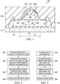
- FIG. 1 illustrates an example of a device 100, which includes a semiconductor chip 101 with terminals 106.
- a portion of the surface of chip 101 is suitable for the attachment of a MEMS device 150.
- the MEMS is stress sensitive.
- An example chip 101 may square shaped, have a side length of several millimeters, such as 2.5 mm, and include a fully functional integrated circuit.
- chip 101 is attached to the pad 110 of a leadframe, preferably using an adhesive epoxy-based polymeric compound 120.
- the terminals 106 of chip 101 are connected by bonding wires 181 to respective leads 111 of a metallic leadframe; the preferred wire metal is a copper alloy, but alternatively gold or aluminum may be used.
- the vertical assembly of MEMS, chip, and portions of the leadframe chip 101 is embedded in an insulating package 190, preferably made of an epoxy-based molding compound.
- the leadframe belongs to the quad flat no-lead (QFN) or in Small Outline No-Lead (SON) families.
- QFN quad flat no-lead
- SON Small Outline No-Lead
- These leadframes are preferably made from a flat sheet of a base metal, which is selected from a group including copper, copper alloys, aluminum, aluminum alloys, iron-nickel alloys, and Kovar.
- the parallel surfaces of the leadframe base metal are treated to create strong affinity for adhesion to plastic compound, especially molding compounds.
- the surfaces of copper leadframes may be oxidized, because copper oxide surfaces are known to exhibit good adhesion to molding compounds.
- Other methods include plasma treatment (described hereinbelow) of the surfaces, or deposition of thin layers of other metals on the base metal surface.
- plated layers of tin have been used, or a layer of nickel (about 0.5 to 2.0 ⁇ m thick) followed by a layer of palladium (about 0.01 to 0.1 ⁇ m thick) optionally followed by an outermost layer of gold (0.003 to 0.009 ⁇ m thick).
- leadframes with a chip attachment pad such as leadframes with elongated leads, with cantilevered leads, or with frames having one or more pads in a plane offset from the plane of the leads.
- Still other embodiments may use laminated substrates made of insulating material alternating with conductive layers. These substrates may have an area suitable for attaching one or more chips, and conductive connections suitable for stitch bonding wires.
- one surface of chip 101 is attached to leadframe pad 110 by epoxy-based compound 120, the opposite chip surface includes an area of diameter 151 suitable for vertically attaching MEMS device 150 using compound 140.
- the compound 140 is made of a silicone compound with a comparatively very low modulus of ⁇ 10 MPa.
- compound 140 may be a silicone compound commercially available from Dow Corning Corporation (Corporate Center, Midland, Michigan, USA).
- the compound may be further characterized by low viscosity and thixotropic behavior so that it exhibits weakened constitution when disturbed and strengthened behavior when left standing.
- the modulus of a material characterizes its strain response to an applied stress (or pressure)
- compound 140 has very compliant mechanical characteristics. This feature is essential to protect the stress-sensitive MEMS, because low modulus material does not transmit stress but rather distributes and absorbs stress. Consequently, low modulus materials, when applied to a side of a stress-sensitive device such as a MEMS, can protect this device against external stress from the covered side.
- the stress-protecting characteristics of material 140 must be preserved through the silicone polymerization cycle occurring during the elevated temperature required for the wire-bonding the MEMS terminals (see hereinbelow).
- the surrounding cocoon of stress-absorbing and stress-dispersing material has to have a thickness suitable to perform functions in conjunction with semiconductor products.
- the material has to have a thickness permitting the attachment of the MEMS to portions of the semiconductor device.
- the material has to have a thickness to allow the incorporation of arching spans of bonding wires.
- FIG. 1 shows that the diameter 151 of the silicone attachment layer is positioned within the inner diameter 131 of a ring 130 of polyimide material. However, the terminals 106 of chip 101 remain outside ring 130.
- Ring 130 is made of a polyimide compound.
- the configuration of ring 130 as a circle, a rectangle, or any other closed structure is patterned from a polyimide layer deposited on a semiconductor (preferably silicon) wafer, which includes multiple chips with integrated circuits (ICs).
- the polyimide ring is made non-wettable and repellent to silicone materials by reducing the polyimide surface energy in a process cycle, which includes a first curing cycle followed by an ashing process and then in turn by a second curing cycle.
- materials other than polyimide may be used if they have silicone-repellent surface characteristics.
- the IC chips are singulated from the wafer. Each chip is then attached to the pad of a substrate, such as to the pad 110 of a metallic leadframe as shown in FIG. 1 .
- the adhesive used for the attachment layer 120 is preferably an epoxy-based polymeric formulation.
- the stress-sensitive MEMS 150 is stacked vertically on IC chip 101 by low modulus silicone layer 140 so that the attachment is inside diameter 131 of the silicone ring 130; layer 140 protects MEMS 150 against stress from the direction of chip 101.
- terminals of MEMS 150 can be connected to contact pads 105 of chip 101 using bonding wires 180.
- Pads 105 are located inside diameter 131 of silicone ring 130.
- chip terminals 106 are connected to substrate connectors (such as leadframe leads 111) using bonding wires 181.
- MEMS 150 is surrounded by a glob 160, which also covers bonding wires 180 and pads 105 and therefore has a dome-shaped configuration.
- Glob 160 is made of low modulus silicone material, preferably the same silicone material as layer 140.
- the silicone of glob 160 may be a silicone commercially available from Dow Corning Corporation. The silicone material is selected so that is has hydrophobic and non-adhesive characteristics towards the polymeric molding formulation, which has been selected as encapsulation compound.
- the viscosity, modulus, and thixotropic index of the silicone material is selected so that glob 160 can be dispensed in a precision volume and glob 160 is restricted to the surface area inside the polyimide ring 130 and does not bleed out across the ring.
- the silicone compound of glob 160 is polymerized in a curing process. Thereafter, glob 160 surrounds the non-attached five sides of the hexahedron-shaped MEMS device and its connecting wire bonds. Glob 160 may have approximately the shape of a hemisphere. Together with the low modulus silicone compound of the attach material, all six sides of the MEMS devices are thus surrounded by low modulus material operable to protect the MEMS against any stress by blunting, dispersing and absorbing external stress arriving at the glob surface.
- the embodiment of FIG. 1 depicts an encapsulation material 190 forming the package for a device 100 belonging to the QFN/SON product families. Other embodiments may belong to different product families.
- package material 190 Independent of the actual configuration of the package and the leadframe, package material 190 must not affect the operation of MEMS 150. Consequently, for the stress-sensitive MEMS of FIG. 1 , this requirement means that package material 190 must adhere strongly to all parts packaged inside (to prevent delamination) except to blob 160 surrounding MEMS 150. Two methods achieve this goal, and the different process flows are discussed hereinbelow.
- FIG. 1 indicates a surface 160a of glob 160 with a layer 170 on the surface.
- surface 160a Based on the first process flow (described in FIGS. 3 and 4 ), surface 160a has been activated by plasma etching and thereafter covered by layer 170 comprising cured low modulus silicone compound.
- the packaging compound 190 will not adhere to layer 170 made of cured (and thus de-activated) silicone compound.
- surface 160a Based on the second process flow (described in FIGS. 3 and 5 ), surface 160a constitutes cured (and thus de-activated) low modulus silicone, which will not adhere to the packaging compound 190, and is covered by layer 170 comprising cured epoxy compound.
- the packaging compound 190 also an epoxy compound, will adhere to and eventually even merge into layer 170 and face the non-adhesive cured silicone surface 160a.
- packaging compound 190 (preferably a molding compound) will not adhere to the cured glob 160 and thus cannot transmit external stress into the glob 160 and to the stress-sensitive MEMS 150. Consequently, MEMS 150 can operate undisturbed by external stress.
- Another embodiment is a method to fabricate a common package for a stress-sensitive microelectromechanical system (MEMS) vertically stacked onto a semiconductor circuitry chip.
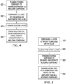
- the method is described as a process flow, which includes processes ( Fig. 2 ) performed in a semiconductor wafer factory and processes (either FIGS. 3 and 4 , or FIGS. 3 and 5 ) performed in a semiconductor assembly factory.
- the method starts in a wafer factory by providing a silicon wafer, which contains multiple integrated circuit (IC) chips and has completed the front-end processes for fabricating the ICs.
- IC integrated circuit
- the intention is to couple a discrete IC chip with a stress-sensitive MEMS and unite them in a common package executed so that the IC and the MEMS can operate undisturbed.
- the process flow begins with the processes listed in FIG. 2 .
- a semiconductor wafer which includes multiple chips with integrated circuits (ICs).
- ICs integrated circuits
- a layer of polyimide material is coated over the surface of the chips.
- the polyimide layer is patterned to form a polyimide ring on each chip, wherein the rings have an inner diameter greater than the largest linear dimension of the MEMS device-to-be-assembled.
- a photolithographic method is used which employs sequentially the process of spinning-on a photoresist layer, masking the photoresist, exposing the mask-protected layer to irradiation, and developing the layer.
- the surface energy of the polyimide rings is reduced in process 203 by subjecting the polyimide material consecutively to the processes of curing the polyimide compound for a first time, then ashing the polyimide compound, and finally curing the polyimide compound for a second time.
- the ashing process involves an oxygen plasma and elevated temperatures; alternatively, a hydrogen plasma could be used.
- the reduced surface energy renders the polyimide rings hydrophobic and repellent to low viscosity and low modulus silicone compounds; silicone material deposited inside the polyimide ring will not bleed out across the polyimide rings.
- the IC chips are singulated from the wafer in process 204.
- the discrete chips can be attached to respective assembly pads of a substrate in an assembly factory.
- the assembly pad may be the chip pad of a leadframe, or alternatively the assembly pad of a laminated substrate.
- the chip is attached to the pad using an epoxy-based compound, which may be cured in a later process at elevated temperature (such as during wire bonding).
- the MEMS To attach a MEMS device to the circuitry chip and use only a single and preferably small package for the IC chip and MEMS combination, the MEMS must be vertically attached to the IC chip.
- the MEMS In the process 302 of assembling a MEMS device vertically on an IC chip, the MEMS is attached to the chip surface inside the respective polyimide ring using a layer of low modulus silicone material.
- a layer of low modulus silicone material are commercially available, such as from Dow Corning Corporation (Midland, Michigan).
- an attachment layer thickness between about 20 ⁇ m and 30 ⁇ m may be satisfactory for protection against external stress.
- the silicone of the attachment layer is polymerized before advancing to the wire bonding process.
- wires including gold or copper may be used.
- the wires are usually spanned with an arch from the MEMS terminals to the chip contact pads.
- the process of wire bonding the terminals 106 of the circuitry chip to respective contact pads of the substrate may be performed.
- the bonding wires are made of copper.
- the chip bonding wires are designated 181.
- a glob is formed by dispensing low-modulus silicone material over the MEMS device and the MEMS bonding wires, while restricting the glob to the surface area inside the polyimide ring. Due to the arches of the bonding wires, the glob has a dome-shaped configuration.
- the silicone material of the glob is hydrophobic and non-adhesive to thermoset molding compounds. Due to its low viscosity and thixotropic index, it can be dispensed in precision volume.
- the silicone glob is cured.
- the packaging compound encapsulating the assembly must not adhere to the surface of the glob covering the MEMS, but must adhere reliably to all other surfaces inside the package. This dichotomy of requirements can be achieved by two methodologies.
- process 401 subjects all surfaces to a plasma etch.
- the plasma involving its gas mixture and power for a prescribed time, preferably operates on cooled surfaces.
- the plasma accomplishes thorough cleaning of the surfaces from adsorbed films, especially water monolayers, thereby freeing up electrical bonds. Also, the plasma induces some roughening of the surfaces.
- a layer of the low-modulus silicone material is dispensed onto the surface of the glob in process 402.
- the nozzle of a syringe releases a controlled drop of the silicone material, which hits the glob and spreads out into a layer of not quite uniform thickness. While a major amount of the drop may remain on the impact location of the glob, some material is bleeding out, resulting in a somewhat non-uniform layer as exemplified by layer 170 in FIG. 1 .
- a drop may have a diameter of approximately 30 ⁇ m and create a layer of non-uniform thickness with a height of about 13 ⁇ m height at the maximum.
- the silicone layer is cured.
- the assembly comprising the stress-sensitive MEMS embedded in the stress-blocking glob and vertically attached to the semiconductor circuitry chip is encapsulated in a polymeric molding compound, together with the portion of the substrate, onto which the chip is attached and wire bonded. The integrated device is thus packaged.
- the second methodology is summarized in FIG. 5 .
- a layer of epoxy compound is dispensed onto the surface of the glob in process 501.
- the epoxy may be the same as the molding compound, or it may be a formulation such as CRP-4160G, commercially available from the Sumitomo Corporation, Japan.
- the layer may be uniform, or it may look similar to layer 170 in FIG. 1 . The layer's nature enables it to merge with, or be absorbed into, the polymeric encapsulation compound.
- the epoxy layer is cured.
- all surfaces are subjected to a plasma etch in order to achieve reliable adhesion to molding compounds.
- the plasma involving its gas mixture and power for a prescribed time, preferably operates on cooled surfaces.
- the plasma accomplishes thorough cleaning of the surfaces from adsorbed films, especially water monolayers, thereby freeing up electrical bonds. Also, the plasma induces some roughening of the surfaces. These effects enhance the adhesion to polymeric filler-filled molding compounds.
- the assembly comprising the stress-sensitive MEMS embedded in the stress-blocking glob and vertically attached to the semiconductor circuitry chip is encapsulated in a polymeric molding compound, together with the portion of the substrate, onto which the chip is attached and wire bonded.
- the integrated device is thus packaged.
- embodiments are applicable to products using any type of semiconductor chip, discrete or integrated circuit, and the material of the semiconductor chip may comprise silicon, silicon germanium, gallium arsenide, gallium nitride, or any other semiconductor or compound material used in integrated circuit manufacturing.
- embodiments are applicable to MEMS having parts moving mechanically under the influence of an energy flow (acoustic, thermal, or optical), a pressure, temperature or voltage difference, or an external force or torque.
- Certain MEMS with a membrane, plate or beam are useful as a pressure sensor (such as a microphone or speaker), inertial sensor (such as an accelerometer), or capacitive sensor (such as a strain gauge or RF switch).
- Other MEMS operate as movement sensors for displacement or tilt.
- Bimetal membranes work as temperature sensors.
Landscapes
- Engineering & Computer Science (AREA)
- Microelectronics & Electronic Packaging (AREA)
- Computer Hardware Design (AREA)
- Manufacturing & Machinery (AREA)
- Micromachines (AREA)
- Structures Or Materials For Encapsulating Or Coating Semiconductor Devices Or Solid State Devices (AREA)
- Physics & Mathematics (AREA)
- Plasma & Fusion (AREA)
Description
- This relates generally to semiconductor devices and processes, and more particularly to a method for packaging a microelectromechanical system (MEMS) device and a packaged MEMS device.
- The wide variety of products collectively called microelectromechanical system (MEMS) devices are small, low weight devices on the micrometer to millimeter scale, which may have sensors or mechanically moving parts, and often movable electrical power supplies and controls, or they may have parts sensitive to mechanical, thermal, acoustic, or optical energy. MEMS have been developed to sense mechanical, thermal, chemical, radiant, magnetic, and biological quantities and inputs, and produce signals as outputs. Because of the sensitive parts and moving parts, MEMS have a need for physical and atmospheric protection. Consequently, MEMS are placed on or in a substrate and have to be surrounded by a housing or package, which has to shield the MEMS against ambient and electrical disturbances, and against mechanical and thermal stress.
- A MEMS device integrates mechanical elements, sensors, actuators, and electronics on a common substrate. The manufacturing approach of a MEMS aims at using batch fabrication techniques similar to those used for microelectronics devices. MEMS can thus benefit from mass production and minimized material consumption to lower the manufacturing cost, while trying to exploit the well-controlled integrated circuit technology. The mechanically moving parts and the electrically active parts of a MEMS are fabricated together with the process flow of the electronic integrated circuit (IC) on a semiconductor chip.
- Following the technology trends of miniaturization, integration and cost reduction, recently developed substrates and boards can embed and interconnect chips and packages to reduce board space, thickness and footprint while increasing power management, electrical performance and fields of application. Examples include penetration of integrated boards into the automotive market, wireless products, and industrial applications.
- As examples, integration boards have been successfully applied to embed wafer level packages, passives, power chips, stacked and bonded chips, wireless modules, power modules, generally active and passive devices for applications requiring miniaturized areas and shrinking thickness.
FR2906236 - The invention is set out in the appended set of claims. In described examples, a packaged microelectromechanical system (MEMS) device comprises a circuitry chip attached to a pad of a substrate with leads, and a MEMS vertically attached to the chip surface by a layer of low modulus silicone compound. On the chip surface, the MEMS device is surrounded by a polyimide ring with a surface phobic to silicone compounds. A dome-shaped glob of cured low modulus silicone material covers the MEMS and MEMS terminal bonding wire spans. The glob is restricted to the chip surface area inside the polyimide ring and has a surface non-adhesive to epoxy-based molding compounds. A package of polymeric molding compound encapsulates a vertical assembly of the glob embedding the MEMS, the chip, and portions of the substrate; the molding compound is non-adhering to the glob surface yet adhering to all other surfaces.
-
-
FIG. 1 depicts a cross section of an integrated polymeric-packaged device including a stress-sensitive MEMS device vertically assembly on a circuitry chip attached to a substrate, wherein the MEMS is surrounded by a protective low-modulus material. -
FIG. 2 shows a diagram of the process flow in a semiconductor wafer fabrication according to example embodiments. -
FIG. 3 displays a portion of a process flow in a semiconductor assembly factory according to example embodiments. -
FIG. 4 depicts another portion of a process flow in a semiconductor assembly factory according to example embodiments. -
FIG. 5 shows yet another portion of a process flow in a semiconductor assembly factory according to example embodiments. - A general trend of the electronic industry requires fewer and smaller components in a system. In this trend, a technical and market advantage will be awarded when the number of components in a system is reduced and the product consumes less space and operating power yet offers improved electrical characteristics and higher reliability. For semiconductor devices, a particular advantage can be gained, when a low cost packaging technology can be realized so that it promotes miniaturization by integrating or eliminating parts, and protection by absorbing or shielding disturbances.
- As for microelectromechanical systems (MEMS), a particular performance and market advantage can be obtained when a MEMS device can be stacked on an existing electronic circuit device already in production, and the same device package can be used. The problem to be solved in each case is the requirement to perform the processes of stacking and packaging so that the specific parameter-to-be-monitored by the MEMS under consideration remains unaffected and the package is shielding the new device effectively against disturbances of the parameter-to-be-monitored.
- For a MEMS of high sensitivity to mechanical and thermal stresses, as a solution to the problem of device integration and protection against mechanical and thermal stress disturbances, a process flow has a unique application of low modulus material and a unique set of process steps to protect the stress-sensitive MEMS device while still using standard, low cost package assembly material and assembly methods practiced in production.
- The integration of unique materials and process steps into the material set and process flow used to assemble standard molded packages, such as quad flat no-lead (QFN) packages, includes a polyimide ring with phobic surface characteristics deposited on a circuitry chip; low modulus silicone compounds and methods to dispense these compounds under controlled conditions to surround hexahedron-shaped MEMS devices on all sides; and controlled component adhesion to polymeric packaging compounds.
-
FIG. 1 illustrates an example of adevice 100, which includes asemiconductor chip 101 withterminals 106. A portion of the surface ofchip 101 is suitable for the attachment of aMEMS device 150. In this example, the MEMS is stress sensitive. Anexample chip 101 may square shaped, have a side length of several millimeters, such as 2.5 mm, and include a fully functional integrated circuit. InFIG. 1 ,chip 101 is attached to thepad 110 of a leadframe, preferably using an adhesive epoxy-basedpolymeric compound 120. Theterminals 106 ofchip 101 are connected bybonding wires 181 to respective leads 111 of a metallic leadframe; the preferred wire metal is a copper alloy, but alternatively gold or aluminum may be used. The vertical assembly of MEMS, chip, and portions of theleadframe chip 101 is embedded in aninsulating package 190, preferably made of an epoxy-based molding compound. - In the example device of
FIG. 1 , the leadframe belongs to the quad flat no-lead (QFN) or in Small Outline No-Lead (SON) families. These leadframes are preferably made from a flat sheet of a base metal, which is selected from a group including copper, copper alloys, aluminum, aluminum alloys, iron-nickel alloys, and Kovar. For many devices, the parallel surfaces of the leadframe base metal are treated to create strong affinity for adhesion to plastic compound, especially molding compounds. As an example, the surfaces of copper leadframes may be oxidized, because copper oxide surfaces are known to exhibit good adhesion to molding compounds. Other methods include plasma treatment (described hereinbelow) of the surfaces, or deposition of thin layers of other metals on the base metal surface. As an example for copper leadframes, plated layers of tin have been used, or a layer of nickel (about 0.5 to 2.0 µm thick) followed by a layer of palladium (about 0.01 to 0.1 µm thick) optionally followed by an outermost layer of gold (0.003 to 0.009 µm thick). - Other embodiments may use other types of leadframes with a chip attachment pad, such as leadframes with elongated leads, with cantilevered leads, or with frames having one or more pads in a plane offset from the plane of the leads. Still other embodiments may use laminated substrates made of insulating material alternating with conductive layers. These substrates may have an area suitable for attaching one or more chips, and conductive connections suitable for stitch bonding wires.
- As
FIG. 1 illustrates, one surface ofchip 101 is attached toleadframe pad 110 by epoxy-basedcompound 120, the opposite chip surface includes an area ofdiameter 151 suitable for vertically attachingMEMS device 150 usingcompound 140. However, in contrast to thepolymeric attach compound 120 with a modulus of > 2GPa, thecompound 140 is made of a silicone compound with a comparatively very low modulus of < 10 MPa. - As an example,
compound 140 may be a silicone compound commercially available from Dow Corning Corporation (Corporate Center, Midland, Michigan, USA). The compound may be further characterized by low viscosity and thixotropic behavior so that it exhibits weakened constitution when disturbed and strengthened behavior when left standing. Because the modulus of a material characterizes its strain response to an applied stress (or pressure),compound 140 has very compliant mechanical characteristics. This feature is essential to protect the stress-sensitive MEMS, because low modulus material does not transmit stress but rather distributes and absorbs stress. Consequently, low modulus materials, when applied to a side of a stress-sensitive device such as a MEMS, can protect this device against external stress from the covered side. The stress-protecting characteristics ofmaterial 140 must be preserved through the silicone polymerization cycle occurring during the elevated temperature required for the wire-bonding the MEMS terminals (see hereinbelow). - To protect a stress sensitive hexahedron-shaped MEMS on all sides against external stress in conjunction with semiconductor devices, the surrounding cocoon of stress-absorbing and stress-dispersing material has to have a thickness suitable to perform functions in conjunction with semiconductor products. As an example, the material has to have a thickness permitting the attachment of the MEMS to portions of the semiconductor device. As another example, the material has to have a thickness to allow the incorporation of arching spans of bonding wires.
-
FIG. 1 shows that thediameter 151 of the silicone attachment layer is positioned within theinner diameter 131 of aring 130 of polyimide material. However, theterminals 106 ofchip 101 remainoutside ring 130.Ring 130 is made of a polyimide compound. As described hereinbelow, the configuration ofring 130 as a circle, a rectangle, or any other closed structure, is patterned from a polyimide layer deposited on a semiconductor (preferably silicon) wafer, which includes multiple chips with integrated circuits (ICs). After patterning, the polyimide ring is made non-wettable and repellent to silicone materials by reducing the polyimide surface energy in a process cycle, which includes a first curing cycle followed by an ashing process and then in turn by a second curing cycle. In examples not forming part of the invention materials other than polyimide may be used if they have silicone-repellent surface characteristics. - After the polyimide ring is made repellent, the IC chips are singulated from the wafer. Each chip is then attached to the pad of a substrate, such as to the
pad 110 of a metallic leadframe as shown inFIG. 1 . The adhesive used for theattachment layer 120 is preferably an epoxy-based polymeric formulation. - In the example of
FIG. 1 , the stress-sensitive MEMS 150 is stacked vertically onIC chip 101 by lowmodulus silicone layer 140 so that the attachment is insidediameter 131 of thesilicone ring 130;layer 140 protectsMEMS 150 against stress from the direction ofchip 101. After the MEMS attachment, terminals ofMEMS 150 can be connected to contact pads 105 ofchip 101 usingbonding wires 180. Pads 105 are located insidediameter 131 ofsilicone ring 130. Thereafter,chip terminals 106 are connected to substrate connectors (such as leadframe leads 111) usingbonding wires 181. - As
FIG. 1 illustrates,MEMS 150 is surrounded by aglob 160, which also coversbonding wires 180 and pads 105 and therefore has a dome-shaped configuration.Glob 160 is made of low modulus silicone material, preferably the same silicone material aslayer 140. As an example, the silicone ofglob 160 may be a silicone commercially available from Dow Corning Corporation. The silicone material is selected so that is has hydrophobic and non-adhesive characteristics towards the polymeric molding formulation, which has been selected as encapsulation compound. The viscosity, modulus, and thixotropic index of the silicone material is selected so thatglob 160 can be dispensed in a precision volume andglob 160 is restricted to the surface area inside thepolyimide ring 130 and does not bleed out across the ring. - After the dispensing process, the silicone compound of
glob 160 is polymerized in a curing process. Thereafter,glob 160 surrounds the non-attached five sides of the hexahedron-shaped MEMS device and its connecting wire bonds.Glob 160 may have approximately the shape of a hemisphere. Together with the low modulus silicone compound of the attach material, all six sides of the MEMS devices are thus surrounded by low modulus material operable to protect the MEMS against any stress by blunting, dispersing and absorbing external stress arriving at the glob surface. - The
device including MEMS 150 stacked oncircuit chip 101, which in turn is mounted onsubstrate 110, must be in a rigid and strong package. The embodiment ofFIG. 1 depicts anencapsulation material 190 forming the package for adevice 100 belonging to the QFN/SON product families. Other embodiments may belong to different product families. Independent of the actual configuration of the package and the leadframe,package material 190 must not affect the operation ofMEMS 150. Consequently, for the stress-sensitive MEMS ofFIG. 1 , this requirement means thatpackage material 190 must adhere strongly to all parts packaged inside (to prevent delamination) except to blob 160 surroundingMEMS 150. Two methods achieve this goal, and the different process flows are discussed hereinbelow. -
FIG. 1 indicates asurface 160a ofglob 160 with alayer 170 on the surface. Based on the first process flow (described inFIGS. 3 and4 ),surface 160a has been activated by plasma etching and thereafter covered bylayer 170 comprising cured low modulus silicone compound. Thepackaging compound 190 will not adhere to layer 170 made of cured (and thus de-activated) silicone compound.Based on the second process flow (described inFIGS. 3 and5 ),surface 160a constitutes cured (and thus de-activated) low modulus silicone, which will not adhere to thepackaging compound 190, and is covered bylayer 170 comprising cured epoxy compound. Thepackaging compound 190, also an epoxy compound, will adhere to and eventually even merge intolayer 170 and face the non-adhesive curedsilicone surface 160a. - In summary, by either one of these methods, packaging compound 190 (preferably a molding compound) will not adhere to the cured
glob 160 and thus cannot transmit external stress into theglob 160 and to the stress-sensitive MEMS 150. Consequently,MEMS 150 can operate undisturbed by external stress. - Another embodiment is a method to fabricate a common package for a stress-sensitive microelectromechanical system (MEMS) vertically stacked onto a semiconductor circuitry chip. The method is described as a process flow, which includes processes (
Fig. 2 ) performed in a semiconductor wafer factory and processes (eitherFIGS. 3 and4 , orFIGS. 3 and5 ) performed in a semiconductor assembly factory. - The method starts in a wafer factory by providing a silicon wafer, which contains multiple integrated circuit (IC) chips and has completed the front-end processes for fabricating the ICs. The intention is to couple a discrete IC chip with a stress-sensitive MEMS and unite them in a common package executed so that the IC and the MEMS can operate undisturbed. The process flow begins with the processes listed in
FIG. 2 . - In the
first step 201 of the process flow, a semiconductor wafer is provided, which includes multiple chips with integrated circuits (ICs). Inprocess 202, a layer of polyimide material is coated over the surface of the chips. Then, the polyimide layer is patterned to form a polyimide ring on each chip, wherein the rings have an inner diameter greater than the largest linear dimension of the MEMS device-to-be-assembled. For the patterning process, a photolithographic method is used which employs sequentially the process of spinning-on a photoresist layer, masking the photoresist, exposing the mask-protected layer to irradiation, and developing the layer. - After the patterning, the surface energy of the polyimide rings is reduced in
process 203 by subjecting the polyimide material consecutively to the processes of curing the polyimide compound for a first time, then ashing the polyimide compound, and finally curing the polyimide compound for a second time. The ashing process involves an oxygen plasma and elevated temperatures; alternatively, a hydrogen plasma could be used. The reduced surface energy renders the polyimide rings hydrophobic and repellent to low viscosity and low modulus silicone compounds; silicone material deposited inside the polyimide ring will not bleed out across the polyimide rings. The IC chips are singulated from the wafer inprocess 204. - In
process 301, the discrete chips can be attached to respective assembly pads of a substrate in an assembly factory. The assembly pad may be the chip pad of a leadframe, or alternatively the assembly pad of a laminated substrate. Preferably, the chip is attached to the pad using an epoxy-based compound, which may be cured in a later process at elevated temperature (such as during wire bonding). - To attach a MEMS device to the circuitry chip and use only a single and preferably small package for the IC chip and MEMS combination, the MEMS must be vertically attached to the IC chip. In the process 302 of assembling a MEMS device vertically on an IC chip, the MEMS is attached to the chip surface inside the respective polyimide ring using a layer of low modulus silicone material. Such materials are commercially available, such as from Dow Corning Corporation (Midland, Michigan). For the low modulus material, an attachment layer thickness between about 20 µm and 30 µm may be satisfactory for protection against external stress. Preferably, the silicone of the attachment layer is polymerized before advancing to the wire bonding process.
- For the process of wire bonding the terminals of the MEMS device to respective contact pads on the chip surface inside the ring, wires including gold or copper may be used. During the bonding operation, the wires are usually spanned with an arch from the MEMS terminals to the chip contact pads.
- In conjunction with the wire bonding process for the MEMS, the process of wire bonding the
terminals 106 of the circuitry chip to respective contact pads of the substrate may be performed. Preferably, the bonding wires are made of copper. InFIG. 1 , the chip bonding wires are designated 181. - In
process 303, a glob is formed by dispensing low-modulus silicone material over the MEMS device and the MEMS bonding wires, while restricting the glob to the surface area inside the polyimide ring. Due to the arches of the bonding wires, the glob has a dome-shaped configuration. The silicone material of the glob is hydrophobic and non-adhesive to thermoset molding compounds. Due to its low viscosity and thixotropic index, it can be dispensed in precision volume. Inprocess 304, the silicone glob is cured. - Because the MEMS of the example embodiment of
FIG. 1 is stress sensitive and has to be protected against transmission of stress, and because the MEMS shares the same overall package with the circuitry chip, the packaging compound encapsulating the assembly must not adhere to the surface of the glob covering the MEMS, but must adhere reliably to all other surfaces inside the package. This dichotomy of requirements can be achieved by two methodologies. - The first methodology is summarized in
FIG. 4 . To achieve good adhesion to molding compounds,process 401 subjects all surfaces to a plasma etch. The plasma, involving its gas mixture and power for a prescribed time, preferably operates on cooled surfaces. The plasma accomplishes thorough cleaning of the surfaces from adsorbed films, especially water monolayers, thereby freeing up electrical bonds. Also, the plasma induces some roughening of the surfaces. These effects enhance the adhesion to polymeric filler-filled molding compounds. - Because the cured silicone of the glob has been affected by the plasma of
process 401, the glob needs an additional process so that it effectively returns to its original low modulus characteristic. To that end, a layer of the low-modulus silicone material is dispensed onto the surface of the glob inprocess 402. The nozzle of a syringe releases a controlled drop of the silicone material, which hits the glob and spreads out into a layer of not quite uniform thickness. While a major amount of the drop may remain on the impact location of the glob, some material is bleeding out, resulting in a somewhat non-uniform layer as exemplified bylayer 170 inFIG. 1 . For the dimensions of the example inFIG. 1 , a drop may have a diameter of approximately 30 µm and create a layer of non-uniform thickness with a height of about 13 µm height at the maximum. - In
process 403, the silicone layer is cured. Then, inprocess 404, the assembly comprising the stress-sensitive MEMS embedded in the stress-blocking glob and vertically attached to the semiconductor circuitry chip is encapsulated in a polymeric molding compound, together with the portion of the substrate, onto which the chip is attached and wire bonded. The integrated device is thus packaged. - The second methodology is summarized in
FIG. 5 . After the processes of forming a dome-shaped glob by dispensing a low-modulus silicone material over the MEMS and the wire spans, and curing the silicone glob, described hereinabove inprocesses process 501. The epoxy may be the same as the molding compound, or it may be a formulation such as CRP-4160G, commercially available from the Sumitomo Corporation, Japan. The layer may be uniform, or it may look similar tolayer 170 inFIG. 1 . The layer's nature enables it to merge with, or be absorbed into, the polymeric encapsulation compound. - In
process 502, the epoxy layer is cured. Then, inprocess 503, all surfaces are subjected to a plasma etch in order to achieve reliable adhesion to molding compounds. The plasma, involving its gas mixture and power for a prescribed time, preferably operates on cooled surfaces. The plasma accomplishes thorough cleaning of the surfaces from adsorbed films, especially water monolayers, thereby freeing up electrical bonds. Also, the plasma induces some roughening of the surfaces. These effects enhance the adhesion to polymeric filler-filled molding compounds. - In
process 504, the assembly comprising the stress-sensitive MEMS embedded in the stress-blocking glob and vertically attached to the semiconductor circuitry chip is encapsulated in a polymeric molding compound, together with the portion of the substrate, onto which the chip is attached and wire bonded. The integrated device is thus packaged. - For example, embodiments are applicable to products using any type of semiconductor chip, discrete or integrated circuit, and the material of the semiconductor chip may comprise silicon, silicon germanium, gallium arsenide, gallium nitride, or any other semiconductor or compound material used in integrated circuit manufacturing.
- As another example, embodiments are applicable to MEMS having parts moving mechanically under the influence of an energy flow (acoustic, thermal, or optical), a pressure, temperature or voltage difference, or an external force or torque. Certain MEMS with a membrane, plate or beam are useful as a pressure sensor (such as a microphone or speaker), inertial sensor (such as an accelerometer), or capacitive sensor (such as a strain gauge or RF switch). Other MEMS operate as movement sensors for displacement or tilt. Bimetal membranes work as temperature sensors.
- Modifications are possible in the described embodiments, and other embodiments are possible, within the scope of the claims.
Claims (14)
- A method for packaging an integrated microelectromechanical system, MEMS, device (150) comprising:providing a semiconductor chip (101) including circuitry with first and second terminals (106), the chip surface having a polyimide ring (130) surrounding an area greater than the footprint of the MEMS and including the first terminals, the surface of the ring having reduced energy rendering the polyimide ring hydrophobic and repellent to silicone compounds;attaching the chip (101) on an assembly pad (110) of a substrate having leads (111);attaching the MEMS device (150) on the chip area inside the polyimide ring (130) using a layer (140) of low modulus silicone material;spanning bonding wires (180) from the terminals of the MEMS to the first circuitry terminals inside the ring;forming a dome-shaped glob (160) by dispensing a low-modulus silicone material over the MEMS and the wire spans, restricting the glob to the chip surface area inside the polyimide ring, the silicone material hydrophobic and non-adhesive to epoxy-based molding compounds;curing the silicone glob, thereby completing the integration of the MEMS and the chip;subjecting all surfaces to a plasma etch for enhancing adhesion to molding compounds;dispensing a layer (170) of the low-modulus silicone material onto the surface of the glob;curing the silicone layer (170) and encapsulating the integrated device including the MEMS (150) embedded by the glob (160), the circuitry chip (101) and portions of the substrate in a polymeric molding compound (190), thereby packaging the integrated device, wherein the molding compound is non adhesive to silicone and non-adhering to the glob surface yet adhering to all other surfaces.
- The method of claim 1, wherein the low modulus silicone material has a modulus < 10 MPa.
- The method of claim 1, wherein the reduced surface energy of the polyimide ring (130) renders the polyimide surface non-wettable and repellent to silicone material, thus preventing bleeding of the silicone material across the ring surface when dispensed.
- The method of claim 1, further including, before the process of forming a dome-shaped glob (160), the process of wire bonding the second terminals (106) of the chip circuitry to respective leads (181) of the substrate.
- The method of claim 1, wherein the substrate is a leadframe having a chip assembly pad (110) and leads (111).
- The method of claim 5, wherein the leadframe is a quad flat no-lead, QFN, leadframe.
- The method of claim 1, wherein the polymeric packaging compound is an epoxy-based thermoset molding formulation including inorganic filler particles.
- The method of claim 1, wherein the process of attaching the chip (101) uses an epoxy-based polymeric compound.
- The method of claim 1, further including, before the process of providing a semiconductor chip (101), the processes of:providing a silicon wafer having a plurality of integrated circuitry chips with first and second terminals (106);coating a layer of polyimide material over the surface of the plurality of chips;patterning the polyimide layer to form a ring (130) on each chip, each ring surrounding an area greater than the footprint of the MEMS (150) and including the first terminals, the patterning process using a photolithographic method including the processes of spinning-on a photoresist layer, and masking, exposing, and developing the layer; andreducing the surface energy of the polyimide rings (130) by subjecting the polyimide material consecutively to the processes of curing a first time, ashing, and curing a second time.
- The method of claim 9, wherein the ashing process includes an oxygen plasma and elevated temperature.
- A packaged microelectromechanical system, MEMS, device comprising:a semiconductor chip (101) including circuitry with first and second terminals (106), of the chip attached to the pad (110) of a substrate having leads (111), the second chip terminals (106) wire bonded to the leads;a MEMS device (150) vertically attached to the chip surface by a layer of low modulus silicone compound (140), the MEMS terminals bonded by wire spans (180) to the first chip terminals;a polyimide ring (130) on the chip surface surrounding the MEMS device (150) and the first terminals, the surface of the ring phobic to silicone compounds;a dome-shaped glob (160) of cured low modulus silicone material covering the MEMS and the MEMS wire spans (180), the glob restricted to the chip surface area inside the polyimide ring, the glob surface non-adhesive to epoxy-based molding compounds; anda package (190) of polymeric molding compound encapsulating the vertical assembly of the glob (160) embedding the MEMS (150), the circuitry chip (101) and portions of the substrate, wherein the molding compound is non adhesive to silicone and non-adhering to the glob surface yet adhering to all other surfaces.
- The device of claim 11, wherein the MEMS (150) is stress sensitive.
- The device of claim 11, wherein the low modulus silicone compound has a modulus < 10 MPa.
- The device of claim 11, wherein the polymeric molding compound is an epoxy-based thermoset molding compound.
Applications Claiming Priority (3)
| Application Number | Priority Date | Filing Date | Title |
|---|---|---|---|
| US201662278224P | 2016-01-13 | 2016-01-13 | |
| US15/134,574 US9896330B2 (en) | 2016-01-13 | 2016-04-21 | Structure and method for packaging stress-sensitive micro-electro-mechanical system stacked onto electronic circuit chip |
| PCT/US2017/013507 WO2017123998A1 (en) | 2016-01-13 | 2017-01-13 | Structure and method for packaging stress-sensitive mems |
Publications (3)
| Publication Number | Publication Date |
|---|---|
| EP3403275A1 EP3403275A1 (en) | 2018-11-21 |
| EP3403275A4 EP3403275A4 (en) | 2019-03-06 |
| EP3403275B1 true EP3403275B1 (en) | 2025-03-12 |
Family
ID=59275431
Family Applications (1)
| Application Number | Title | Priority Date | Filing Date |
|---|---|---|---|
| EP17739078.8A Active EP3403275B1 (en) | 2016-01-13 | 2017-01-13 | Structure and method for packaging stress-sensitive mems |
Country Status (5)
| Country | Link |
|---|---|
| US (4) | US9896330B2 (en) |
| EP (1) | EP3403275B1 (en) |
| JP (2) | JP6974685B2 (en) |
| CN (2) | CN116692765A (en) |
| WO (1) | WO2017123998A1 (en) |
Families Citing this family (28)
| Publication number | Priority date | Publication date | Assignee | Title |
|---|---|---|---|---|
| US9896330B2 (en) * | 2016-01-13 | 2018-02-20 | Texas Instruments Incorporated | Structure and method for packaging stress-sensitive micro-electro-mechanical system stacked onto electronic circuit chip |
| CN109075139B (en) * | 2016-05-19 | 2022-12-27 | 森西欧有限公司 | Integrated circuit package and method of manufacturing the same |
| EP3260821B1 (en) * | 2016-06-21 | 2019-09-11 | ams International AG | Sensor package and method of producing the sensor package |
| US10635205B1 (en) * | 2017-03-08 | 2020-04-28 | Cit Rogene, Inc | Flexible microstructured and textured metamaterials |
| FR3073080B1 (en) * | 2017-10-26 | 2021-01-08 | St Microelectronics Srl | INTEGRATED CIRCUIT IN QFN BOX |
| US10861741B2 (en) | 2017-11-27 | 2020-12-08 | Texas Instruments Incorporated | Electronic package for integrated circuits and related methods |
| US10370244B2 (en) * | 2017-11-30 | 2019-08-06 | Infineon Technologies Ag | Deposition of protective material at wafer level in front end for early stage particle and moisture protection |
| US10516381B2 (en) | 2017-12-29 | 2019-12-24 | Texas Instruments Incorporated | 3D-printed protective shell structures for stress sensitive circuits |
| US11538767B2 (en) * | 2017-12-29 | 2022-12-27 | Texas Instruments Incorporated | Integrated circuit package with partitioning based on environmental sensitivity |
| CN112334867B (en) | 2018-05-24 | 2025-11-11 | 纽约州立大学研究基金会 | Capacitive sensor |
| US11031311B2 (en) * | 2018-11-21 | 2021-06-08 | Texas Instruments Incorporated | Packaged semiconductor device with multilayer stress buffer |
| US11302611B2 (en) * | 2018-11-28 | 2022-04-12 | Texas Instruments Incorporated | Semiconductor package with top circuit and an IC with a gap over the IC |
| US11404270B2 (en) | 2018-11-30 | 2022-08-02 | Texas Instruments Incorporated | Microelectronic device substrate formed by additive process |
| US10910465B2 (en) | 2018-12-28 | 2021-02-02 | Texas Instruments Incorporated | 3D printed semiconductor package |
| US10861715B2 (en) | 2018-12-28 | 2020-12-08 | Texas Instruments Incorporated | 3D printed semiconductor package |
| US11489511B2 (en) | 2018-12-30 | 2022-11-01 | Texas Instruments Incorporated | Highly dispersive bulk acoustic wave resonators |
| US11394361B2 (en) | 2019-02-25 | 2022-07-19 | Texas Instruments Incorporated | Buk acoustic wave resonator with guard rings having recessed space from electrode edge and periodic designs |
| US11264970B2 (en) | 2019-03-02 | 2022-03-01 | Texas Instruments Incorporated | Piezoelectric resonator with patterned resonant confiners |
| US11190164B2 (en) | 2019-05-24 | 2021-11-30 | Texas Instruments Incorporated | Using acoustic reflector to reduce spurious modes |
| CN110600432A (en) * | 2019-05-27 | 2019-12-20 | 华为技术有限公司 | Packaging structure and mobile terminal |
| US10841710B1 (en) * | 2019-06-20 | 2020-11-17 | Solid State System Co., Ltd. | Package structure of micro-electro-mechanical-system microphone package and method for packaging the same |
| US11356082B2 (en) | 2019-12-12 | 2022-06-07 | Texas Instruments Incorporated | Folded ramp generator |
| DE102020119688A1 (en) * | 2020-07-27 | 2022-01-27 | Infineon Technologies Ag | semiconductor devices with wireless transmitters and/or wireless receivers |
| US11584638B2 (en) * | 2020-07-30 | 2023-02-21 | Invensense, Inc. | Reducing delamination in sensor package |
| US12365584B2 (en) * | 2021-10-26 | 2025-07-22 | Texas Instruments Incorporated | Methods and apparatus for electronic device packaging |
| CN115642095B (en) * | 2022-09-08 | 2024-03-29 | 武汉敏声新技术有限公司 | Radio frequency module packaging structure and method |
| US12483222B2 (en) | 2023-02-24 | 2025-11-25 | Texas Instruments Incorporated | Spurious mode reduction for electromechanical resonator circuit |
| DE102023208534A1 (en) * | 2023-09-05 | 2025-03-06 | Robert Bosch Gesellschaft mit beschränkter Haftung | Sensor system comprising at least one MEMS unit, at least one ASIC unit and a substrate |
Family Cites Families (60)
| Publication number | Priority date | Publication date | Assignee | Title |
|---|---|---|---|---|
| FR1300872A (en) | 1961-06-29 | 1962-08-10 | Quercia Flaminaire Sa | Improvements to gas lighters |
| JPS56112942U (en) * | 1980-01-29 | 1981-08-31 | ||
| JPS58107657A (en) * | 1981-12-21 | 1983-06-27 | Nec Corp | Semiconductor device |
| JPS5942043U (en) * | 1982-09-10 | 1984-03-17 | 富士電機株式会社 | Resin-encapsulated semiconductor device |
| US4814943A (en) | 1986-06-04 | 1989-03-21 | Oki Electric Industry Co., Ltd. | Printed circuit devices using thermoplastic resin cover plate |
| JPS63116451A (en) * | 1986-11-04 | 1988-05-20 | Mitsubishi Electric Corp | Hybrid integrated circuit device |
| JPH0258357A (en) * | 1988-08-24 | 1990-02-27 | Hitachi Ltd | Pin grid array type semiconductor device |
| JPH04171970A (en) * | 1990-11-06 | 1992-06-19 | Matsushita Electric Ind Co Ltd | Semiconductor device |
| US5206794A (en) * | 1991-12-20 | 1993-04-27 | Vlsi Technology, Inc. | Integrated circuit package with device and wire coat assembly |
| US5436203A (en) | 1994-07-05 | 1995-07-25 | Motorola, Inc. | Shielded liquid encapsulated semiconductor device and method for making the same |
| JP3274963B2 (en) * | 1996-04-19 | 2002-04-15 | 株式会社日立製作所 | Semiconductor device |
| US6092281A (en) | 1998-08-28 | 2000-07-25 | Amkor Technology, Inc. | Electromagnetic interference shield driver and method |
| KR20010010858A (en) * | 1999-07-23 | 2001-02-15 | 이수남 | method of fabricating semiconductor package |
| JP2001326304A (en) | 2000-05-15 | 2001-11-22 | Toshiba Corp | Semiconductor device and manufacturing method thereof |
| US6686649B1 (en) | 2001-05-14 | 2004-02-03 | Amkor Technology, Inc. | Multi-chip semiconductor package with integral shield and antenna |
| US6856007B2 (en) | 2001-08-28 | 2005-02-15 | Tessera, Inc. | High-frequency chip packages |
| US7432586B2 (en) | 2004-06-21 | 2008-10-07 | Broadcom Corporation | Apparatus and method for thermal and electromagnetic interference (EMI) shielding enhancement in die-up array packages |
| DE102004043663B4 (en) * | 2004-09-07 | 2006-06-08 | Infineon Technologies Ag | Semiconductor sensor component with cavity housing and sensor chip and method for producing a semiconductor sensor component with cavity housing and sensor chip |
| US20060273441A1 (en) * | 2005-06-04 | 2006-12-07 | Yueh-Chiu Chung | Assembly structure and method for chip scale package |
| US7365371B2 (en) * | 2005-08-04 | 2008-04-29 | Cree, Inc. | Packages for semiconductor light emitting devices utilizing dispensed encapsulants |
| US7244636B2 (en) * | 2005-10-19 | 2007-07-17 | Texas Instruments Incorporated | Semiconductor assembly for improved device warpage and solder ball coplanarity |
| DE102006026023A1 (en) * | 2006-06-01 | 2007-12-06 | Infineon Technologies Ag | Semiconductor component, has plastic compound arranged between another plastic compound and edge sides of adhesive layer and chip and upper side of chip such that latter plastic compound does not have physical contact to chip and layer |
| US8022554B2 (en) * | 2006-06-15 | 2011-09-20 | Sitime Corporation | Stacked die package for MEMS resonator system |
| FR2906236B3 (en) | 2006-09-22 | 2008-08-08 | Sigurdmicroelectronics Corp | STRUCTURE OF REINFORCED MICRO-ELECTROMECHANICAL SYSTEM HOUSING |
| JP4305502B2 (en) | 2006-11-28 | 2009-07-29 | カシオ計算機株式会社 | Manufacturing method of semiconductor device |
| CN101611481A (en) | 2007-01-09 | 2009-12-23 | 英飞凌科技股份有限公司 | semiconductor package |
| FR2911865B1 (en) * | 2007-01-26 | 2009-04-17 | Commissariat Energie Atomique | METHOD FOR PRODUCING A COMPONENT PROTECTION COVER ON A SUBSTRATE |
| US20080197514A1 (en) * | 2007-02-16 | 2008-08-21 | Thomas Goida | Die coat perimeter to enhance semiconductor reliability |
| US20080217761A1 (en) * | 2007-03-08 | 2008-09-11 | Advanced Chip Engineering Technology Inc. | Structure of semiconductor device package and method of the same |
| US20080217708A1 (en) | 2007-03-09 | 2008-09-11 | Skyworks Solutions, Inc. | Integrated passive cap in a system-in-package |
| US7872335B2 (en) | 2007-06-08 | 2011-01-18 | Broadcom Corporation | Lead frame-BGA package with enhanced thermal performance and I/O counts |
| US7843021B2 (en) * | 2008-02-28 | 2010-11-30 | Shandong Gettop Acoustic Co. Ltd. | Double-side mountable MEMS package |
| KR101481577B1 (en) | 2008-09-29 | 2015-01-13 | 삼성전자주식회사 | Semiconductor package having dam of ink jet method and manufacturing method thereof |
| US8231692B2 (en) | 2008-11-06 | 2012-07-31 | International Business Machines Corporation | Method for manufacturing an electronic device |
| US8710682B2 (en) | 2009-09-03 | 2014-04-29 | Designer Molecules Inc, Inc. | Materials and methods for stress reduction in semiconductor wafer passivation layers |
| KR101089956B1 (en) | 2009-10-28 | 2011-12-05 | 삼성전기주식회사 | Flip chip package and manufacturing method thereof |
| US8338208B2 (en) | 2009-12-31 | 2012-12-25 | Texas Instruments Incorporated | Micro-electro-mechanical system having movable element integrated into leadframe-based package |
| JP2011183554A (en) * | 2010-03-04 | 2011-09-22 | Asahi Glass Co Ltd | Method for producing fine structure |
| DE102010030960B4 (en) * | 2010-07-06 | 2020-12-10 | Robert Bosch Gmbh | Process for manufacturing a vibration-damped component |
| US9380380B2 (en) | 2011-01-07 | 2016-06-28 | Stmicroelectronics S.R.L. | Acoustic transducer and interface circuit |
| US8643165B2 (en) * | 2011-02-23 | 2014-02-04 | Texas Instruments Incorporated | Semiconductor device having agglomerate terminals |
| JP2012238796A (en) * | 2011-05-13 | 2012-12-06 | Panasonic Corp | Semiconductor device and manufacturing method of the same |
| US9073748B2 (en) * | 2011-11-10 | 2015-07-07 | Taiwan Semiconductor Manufacturing Company, Ltd. | Microelectro mechanical system encapsulation scheme |
| US8907469B2 (en) | 2012-01-19 | 2014-12-09 | Taiwan Semiconductor Manufacturing Company, Ltd. | Integrated circuit package assembly and method of forming the same |
| US8686550B2 (en) * | 2012-02-13 | 2014-04-01 | Freescale Semiconductor, Inc. | Method and apparatus for high pressure sensor device |
| US9102511B2 (en) * | 2012-06-08 | 2015-08-11 | Texas Instruments Incorporated | Hermetic plastic molded MEMS device package and method of fabrication |
| CN103193198A (en) | 2013-04-22 | 2013-07-10 | 安徽北方芯动联科微系统技术有限公司 | Method for reducing packaging stress of micro-electromechanical system (MEMS) chip through back graphics |
| US9284182B1 (en) | 2013-08-20 | 2016-03-15 | Qualtre, Inc. | MEMS devices anti-stiction coating and encapsulant having opposing water resitive characteristics |
| JP5867465B2 (en) * | 2013-08-22 | 2016-02-24 | Tdk株式会社 | Magnetic sensor |
| ITTO20130775A1 (en) | 2013-09-26 | 2015-03-27 | St Microelectronics Srl | SENSOR DEVICE WITH INTEGRATED CALIBRATION SYSTEM AND METHOD OF CALIBRATION OF THE SAME |
| JP2015106649A (en) * | 2013-11-29 | 2015-06-08 | 株式会社デンソー | Electronic device |
| KR20150072687A (en) * | 2013-12-20 | 2015-06-30 | 삼성전기주식회사 | Gas sensor package |
| JP6523034B2 (en) | 2014-05-09 | 2019-05-29 | 株式会社フジクラ | Semiconductor mounting structure |
| EP3026696B1 (en) * | 2014-11-26 | 2021-03-03 | STMicroelectronics Srl | Package for semiconductor devices sensitive to mechanical and thermo-mechanical stresses, such as mems pressure sensors |
| CN104835808A (en) * | 2015-03-16 | 2015-08-12 | 苏州晶方半导体科技股份有限公司 | Chip packaging method and chip packaging structure |
| US9896330B2 (en) * | 2016-01-13 | 2018-02-20 | Texas Instruments Incorporated | Structure and method for packaging stress-sensitive micro-electro-mechanical system stacked onto electronic circuit chip |
| US10141245B2 (en) | 2016-08-24 | 2018-11-27 | Qorvo Us, Inc. | High-power acoustic device with improved performance |
| KR102551657B1 (en) | 2016-12-12 | 2023-07-06 | 삼성전자주식회사 | EMI shielding structure and manufacturing method for the same |
| US9761543B1 (en) | 2016-12-20 | 2017-09-12 | Texas Instruments Incorporated | Integrated circuits with thermal isolation and temperature regulation |
| US10217649B2 (en) | 2017-06-09 | 2019-02-26 | Advanced Semiconductor Engineering, Inc. | Semiconductor device package having an underfill barrier |
-
2016
- 2016-04-21 US US15/134,574 patent/US9896330B2/en active Active
-
2017
- 2017-01-13 EP EP17739078.8A patent/EP3403275B1/en active Active
- 2017-01-13 CN CN202310770497.4A patent/CN116692765A/en active Pending
- 2017-01-13 CN CN201780006618.0A patent/CN108475645B/en active Active
- 2017-01-13 JP JP2018536857A patent/JP6974685B2/en active Active
- 2017-01-13 WO PCT/US2017/013507 patent/WO2017123998A1/en not_active Ceased
-
2018
- 2018-01-10 US US15/867,563 patent/US10233074B2/en active Active
-
2019
- 2019-02-04 US US16/266,227 patent/US10723616B2/en active Active
-
2020
- 2020-07-28 US US16/941,138 patent/US11498831B2/en active Active
-
2021
- 2021-10-11 JP JP2021166547A patent/JP7298856B2/en active Active
Also Published As
| Publication number | Publication date |
|---|---|
| EP3403275A4 (en) | 2019-03-06 |
| JP2019503277A (en) | 2019-02-07 |
| JP2022008991A (en) | 2022-01-14 |
| US9896330B2 (en) | 2018-02-20 |
| CN108475645A (en) | 2018-08-31 |
| US11498831B2 (en) | 2022-11-15 |
| WO2017123998A1 (en) | 2017-07-20 |
| US20170197823A1 (en) | 2017-07-13 |
| JP7298856B2 (en) | 2023-06-27 |
| JP6974685B2 (en) | 2021-12-01 |
| CN108475645B (en) | 2023-07-18 |
| US20190169019A1 (en) | 2019-06-06 |
| US20200354214A1 (en) | 2020-11-12 |
| EP3403275A1 (en) | 2018-11-21 |
| CN116692765A (en) | 2023-09-05 |
| US10723616B2 (en) | 2020-07-28 |
| US20180127266A1 (en) | 2018-05-10 |
| US10233074B2 (en) | 2019-03-19 |
Similar Documents
| Publication | Publication Date | Title |
|---|---|---|
| US11498831B2 (en) | Structures for packaging stress-sensitive micro-electro-mechanical system stacked onto electronic circuit chip | |
| US12365582B2 (en) | MEMS resonator integrated cicruit fabrication | |
| CN109075129B (en) | floating die package | |
| US9227836B2 (en) | Hermetic plastic molded MEMS device package and method of fabrication | |
| US9952110B2 (en) | Multi-die pressure sensor package | |
| US20140374848A1 (en) | Semiconductor sensor device with metal lid | |
| US20160068387A1 (en) | Semiconductor cavity package using photosensitive resin | |
| US7994646B2 (en) | Semiconductor device | |
| US10741415B2 (en) | Thermosonically bonded connection for flip chip packages | |
| US7745916B2 (en) | Module comprising polymer-containing electrical connecting element |
Legal Events
| Date | Code | Title | Description |
|---|---|---|---|
| STAA | Information on the status of an ep patent application or granted ep patent |
Free format text: STATUS: THE INTERNATIONAL PUBLICATION HAS BEEN MADE |
|
| PUAI | Public reference made under article 153(3) epc to a published international application that has entered the european phase |
Free format text: ORIGINAL CODE: 0009012 |
|
| STAA | Information on the status of an ep patent application or granted ep patent |
Free format text: STATUS: REQUEST FOR EXAMINATION WAS MADE |
|
| 17P | Request for examination filed |
Effective date: 20180813 |
|
| AK | Designated contracting states |
Kind code of ref document: A1 Designated state(s): AL AT BE BG CH CY CZ DE DK EE ES FI FR GB GR HR HU IE IS IT LI LT LU LV MC MK MT NL NO PL PT RO RS SE SI SK SM TR |
|
| AX | Request for extension of the european patent |
Extension state: BA ME |
|
| RIN1 | Information on inventor provided before grant (corrected) |
Inventor name: YANO, GENKI Inventor name: COOK, BENJAMIN Inventor name: WACHTLER, KURT, PETER Inventor name: GOODLIN, BRIAN, E. Inventor name: YOSHINO, MAKOTO Inventor name: KURODA, AYUMU Inventor name: KIRMSE, KAREN Inventor name: JACOBSEN, STUART |
|
| RIN1 | Information on inventor provided before grant (corrected) |
Inventor name: KURODA, AYUMU Inventor name: YOSHINO, MAKOTO Inventor name: COOK, BENJAMIN Inventor name: GOODLIN, BRIAN, E. Inventor name: KIRMSE, KAREN Inventor name: JACOBSEN, STUART Inventor name: YANO, GENKI Inventor name: WACHTLER, KURT, PETER |
|
| A4 | Supplementary search report drawn up and despatched |
Effective date: 20190205 |
|
| RIC1 | Information provided on ipc code assigned before grant |
Ipc: H01L 21/56 20060101ALI20190130BHEP Ipc: H01L 21/461 20060101AFI20190130BHEP Ipc: B81C 1/00 20060101ALI20190130BHEP Ipc: B81B 7/00 20060101ALI20190130BHEP Ipc: H01L 23/492 20060101ALI20190130BHEP |
|
| DAV | Request for validation of the european patent (deleted) | ||
| DAX | Request for extension of the european patent (deleted) | ||
| STAA | Information on the status of an ep patent application or granted ep patent |
Free format text: STATUS: EXAMINATION IS IN PROGRESS |
|
| 17Q | First examination report despatched |
Effective date: 20211015 |
|
| GRAP | Despatch of communication of intention to grant a patent |
Free format text: ORIGINAL CODE: EPIDOSNIGR1 |
|
| STAA | Information on the status of an ep patent application or granted ep patent |
Free format text: STATUS: GRANT OF PATENT IS INTENDED |
|
| INTG | Intention to grant announced |
Effective date: 20240909 |
|
| P01 | Opt-out of the competence of the unified patent court (upc) registered |
Free format text: CASE NUMBER: APP_56046/2024 Effective date: 20241014 |
|
| GRAS | Grant fee paid |
Free format text: ORIGINAL CODE: EPIDOSNIGR3 |
|
| GRAA | (expected) grant |
Free format text: ORIGINAL CODE: 0009210 |
|
| STAA | Information on the status of an ep patent application or granted ep patent |
Free format text: STATUS: THE PATENT HAS BEEN GRANTED |
|
| AK | Designated contracting states |
Kind code of ref document: B1 Designated state(s): AL AT BE BG CH CY CZ DE DK EE ES FI FR GB GR HR HU IE IS IT LI LT LU LV MC MK MT NL NO PL PT RO RS SE SI SK SM TR |
|
| REG | Reference to a national code |
Ref country code: GB Ref legal event code: FG4D |
|
| REG | Reference to a national code |
Ref country code: CH Ref legal event code: EP |
|
| REG | Reference to a national code |
Ref country code: DE Ref legal event code: R096 Ref document number: 602017088297 Country of ref document: DE |
|
| REG | Reference to a national code |
Ref country code: IE Ref legal event code: FG4D |
|
| PG25 | Lapsed in a contracting state [announced via postgrant information from national office to epo] |
Ref country code: RS Free format text: LAPSE BECAUSE OF FAILURE TO SUBMIT A TRANSLATION OF THE DESCRIPTION OR TO PAY THE FEE WITHIN THE PRESCRIBED TIME-LIMIT Effective date: 20250612 |
|
| PG25 | Lapsed in a contracting state [announced via postgrant information from national office to epo] |
Ref country code: FI Free format text: LAPSE BECAUSE OF FAILURE TO SUBMIT A TRANSLATION OF THE DESCRIPTION OR TO PAY THE FEE WITHIN THE PRESCRIBED TIME-LIMIT Effective date: 20250312 |
|
| PG25 | Lapsed in a contracting state [announced via postgrant information from national office to epo] |
Ref country code: ES Free format text: LAPSE BECAUSE OF FAILURE TO SUBMIT A TRANSLATION OF THE DESCRIPTION OR TO PAY THE FEE WITHIN THE PRESCRIBED TIME-LIMIT Effective date: 20250312 |
|
| REG | Reference to a national code |
Ref country code: LT Ref legal event code: MG9D |
|
| PG25 | Lapsed in a contracting state [announced via postgrant information from national office to epo] |
Ref country code: NO Free format text: LAPSE BECAUSE OF FAILURE TO SUBMIT A TRANSLATION OF THE DESCRIPTION OR TO PAY THE FEE WITHIN THE PRESCRIBED TIME-LIMIT Effective date: 20250612 |
|
| PG25 | Lapsed in a contracting state [announced via postgrant information from national office to epo] |
Ref country code: HR Free format text: LAPSE BECAUSE OF FAILURE TO SUBMIT A TRANSLATION OF THE DESCRIPTION OR TO PAY THE FEE WITHIN THE PRESCRIBED TIME-LIMIT Effective date: 20250312 |
|
| REG | Reference to a national code |
Ref country code: NL Ref legal event code: MP Effective date: 20250312 |
|
| PG25 | Lapsed in a contracting state [announced via postgrant information from national office to epo] |
Ref country code: LV Free format text: LAPSE BECAUSE OF FAILURE TO SUBMIT A TRANSLATION OF THE DESCRIPTION OR TO PAY THE FEE WITHIN THE PRESCRIBED TIME-LIMIT Effective date: 20250312 |
|
| PG25 | Lapsed in a contracting state [announced via postgrant information from national office to epo] |
Ref country code: GR Free format text: LAPSE BECAUSE OF FAILURE TO SUBMIT A TRANSLATION OF THE DESCRIPTION OR TO PAY THE FEE WITHIN THE PRESCRIBED TIME-LIMIT Effective date: 20250613 Ref country code: BG Free format text: LAPSE BECAUSE OF FAILURE TO SUBMIT A TRANSLATION OF THE DESCRIPTION OR TO PAY THE FEE WITHIN THE PRESCRIBED TIME-LIMIT Effective date: 20250312 |
|
| REG | Reference to a national code |
Ref country code: AT Ref legal event code: MK05 Ref document number: 1775767 Country of ref document: AT Kind code of ref document: T Effective date: 20250312 |
|
| PG25 | Lapsed in a contracting state [announced via postgrant information from national office to epo] |
Ref country code: NL Free format text: LAPSE BECAUSE OF FAILURE TO SUBMIT A TRANSLATION OF THE DESCRIPTION OR TO PAY THE FEE WITHIN THE PRESCRIBED TIME-LIMIT Effective date: 20250312 |
|
| PG25 | Lapsed in a contracting state [announced via postgrant information from national office to epo] |
Ref country code: SE Free format text: LAPSE BECAUSE OF FAILURE TO SUBMIT A TRANSLATION OF THE DESCRIPTION OR TO PAY THE FEE WITHIN THE PRESCRIBED TIME-LIMIT Effective date: 20250312 |
|
| PG25 | Lapsed in a contracting state [announced via postgrant information from national office to epo] |
Ref country code: SM Free format text: LAPSE BECAUSE OF FAILURE TO SUBMIT A TRANSLATION OF THE DESCRIPTION OR TO PAY THE FEE WITHIN THE PRESCRIBED TIME-LIMIT Effective date: 20250312 |
|
| PG25 | Lapsed in a contracting state [announced via postgrant information from national office to epo] |
Ref country code: PT Free format text: LAPSE BECAUSE OF FAILURE TO SUBMIT A TRANSLATION OF THE DESCRIPTION OR TO PAY THE FEE WITHIN THE PRESCRIBED TIME-LIMIT Effective date: 20250714 |
|
| PG25 | Lapsed in a contracting state [announced via postgrant information from national office to epo] |
Ref country code: IT Free format text: LAPSE BECAUSE OF FAILURE TO SUBMIT A TRANSLATION OF THE DESCRIPTION OR TO PAY THE FEE WITHIN THE PRESCRIBED TIME-LIMIT Effective date: 20250312 Ref country code: PL Free format text: LAPSE BECAUSE OF FAILURE TO SUBMIT A TRANSLATION OF THE DESCRIPTION OR TO PAY THE FEE WITHIN THE PRESCRIBED TIME-LIMIT Effective date: 20250312 |
|
| PG25 | Lapsed in a contracting state [announced via postgrant information from national office to epo] |
Ref country code: AT Free format text: LAPSE BECAUSE OF FAILURE TO SUBMIT A TRANSLATION OF THE DESCRIPTION OR TO PAY THE FEE WITHIN THE PRESCRIBED TIME-LIMIT Effective date: 20250312 |
|
| PG25 | Lapsed in a contracting state [announced via postgrant information from national office to epo] |
Ref country code: EE Free format text: LAPSE BECAUSE OF FAILURE TO SUBMIT A TRANSLATION OF THE DESCRIPTION OR TO PAY THE FEE WITHIN THE PRESCRIBED TIME-LIMIT Effective date: 20250312 Ref country code: CZ Free format text: LAPSE BECAUSE OF FAILURE TO SUBMIT A TRANSLATION OF THE DESCRIPTION OR TO PAY THE FEE WITHIN THE PRESCRIBED TIME-LIMIT Effective date: 20250312 |
|
| PG25 | Lapsed in a contracting state [announced via postgrant information from national office to epo] |
Ref country code: RO Free format text: LAPSE BECAUSE OF FAILURE TO SUBMIT A TRANSLATION OF THE DESCRIPTION OR TO PAY THE FEE WITHIN THE PRESCRIBED TIME-LIMIT Effective date: 20250312 |
|
| PG25 | Lapsed in a contracting state [announced via postgrant information from national office to epo] |
Ref country code: SK Free format text: LAPSE BECAUSE OF FAILURE TO SUBMIT A TRANSLATION OF THE DESCRIPTION OR TO PAY THE FEE WITHIN THE PRESCRIBED TIME-LIMIT Effective date: 20250312 |
|
| PG25 | Lapsed in a contracting state [announced via postgrant information from national office to epo] |
Ref country code: IS Free format text: LAPSE BECAUSE OF FAILURE TO SUBMIT A TRANSLATION OF THE DESCRIPTION OR TO PAY THE FEE WITHIN THE PRESCRIBED TIME-LIMIT Effective date: 20250712 |
|
| REG | Reference to a national code |
Ref country code: DE Ref legal event code: R079 Ref document number: 602017088297 Country of ref document: DE Free format text: PREVIOUS MAIN CLASS: H01L0021461000 Ipc: H10P0052400000 |
|
| REG | Reference to a national code |
Ref country code: DE Ref legal event code: R097 Ref document number: 602017088297 Country of ref document: DE |
|
| PGFP | Annual fee paid to national office [announced via postgrant information from national office to epo] |
Ref country code: GB Payment date: 20251219 Year of fee payment: 10 |
|
| PG25 | Lapsed in a contracting state [announced via postgrant information from national office to epo] |
Ref country code: DK Free format text: LAPSE BECAUSE OF FAILURE TO SUBMIT A TRANSLATION OF THE DESCRIPTION OR TO PAY THE FEE WITHIN THE PRESCRIBED TIME-LIMIT Effective date: 20250312 |
|
| PGFP | Annual fee paid to national office [announced via postgrant information from national office to epo] |
Ref country code: FR Payment date: 20251217 Year of fee payment: 10 |
|
| PLBE | No opposition filed within time limit |
Free format text: ORIGINAL CODE: 0009261 |
|
| STAA | Information on the status of an ep patent application or granted ep patent |
Free format text: STATUS: NO OPPOSITION FILED WITHIN TIME LIMIT |
|
| REG | Reference to a national code |
Ref country code: CH Ref legal event code: L10 Free format text: ST27 STATUS EVENT CODE: U-0-0-L10-L00 (AS PROVIDED BY THE NATIONAL OFFICE) Effective date: 20260121 |
|
| 26N | No opposition filed |
Effective date: 20251215 |
|
| PGFP | Annual fee paid to national office [announced via postgrant information from national office to epo] |
Ref country code: DE Payment date: 20251217 Year of fee payment: 10 |