EP3390894B1 - Led-fassung zur aufnahme einer cob-led und basis für eine solche led-fassung - Google Patents
Led-fassung zur aufnahme einer cob-led und basis für eine solche led-fassung Download PDFInfo
- Publication number
- EP3390894B1 EP3390894B1 EP16711193.9A EP16711193A EP3390894B1 EP 3390894 B1 EP3390894 B1 EP 3390894B1 EP 16711193 A EP16711193 A EP 16711193A EP 3390894 B1 EP3390894 B1 EP 3390894B1
- Authority
- EP
- European Patent Office
- Prior art keywords
- base
- contact element
- led
- radial
- contact
- Prior art date
- Legal status (The legal status is an assumption and is not a legal conclusion. Google has not performed a legal analysis and makes no representation as to the accuracy of the status listed.)
- Active
Links
Images

Classifications
-
- F—MECHANICAL ENGINEERING; LIGHTING; HEATING; WEAPONS; BLASTING
- F21—LIGHTING
- F21V—FUNCTIONAL FEATURES OR DETAILS OF LIGHTING DEVICES OR SYSTEMS THEREOF; STRUCTURAL COMBINATIONS OF LIGHTING DEVICES WITH OTHER ARTICLES, NOT OTHERWISE PROVIDED FOR
- F21V23/00—Arrangement of electric circuit elements in or on lighting devices
- F21V23/06—Arrangement of electric circuit elements in or on lighting devices the elements being coupling devices, e.g. connectors
-
- F—MECHANICAL ENGINEERING; LIGHTING; HEATING; WEAPONS; BLASTING
- F21—LIGHTING
- F21K—NON-ELECTRIC LIGHT SOURCES USING LUMINESCENCE; LIGHT SOURCES USING ELECTROCHEMILUMINESCENCE; LIGHT SOURCES USING CHARGES OF COMBUSTIBLE MATERIAL; LIGHT SOURCES USING SEMICONDUCTOR DEVICES AS LIGHT-GENERATING ELEMENTS; LIGHT SOURCES NOT OTHERWISE PROVIDED FOR
- F21K9/00—Light sources using semiconductor devices as light-generating elements, e.g. using light-emitting diodes [LED] or lasers
-
- F—MECHANICAL ENGINEERING; LIGHTING; HEATING; WEAPONS; BLASTING
- F21—LIGHTING
- F21V—FUNCTIONAL FEATURES OR DETAILS OF LIGHTING DEVICES OR SYSTEMS THEREOF; STRUCTURAL COMBINATIONS OF LIGHTING DEVICES WITH OTHER ARTICLES, NOT OTHERWISE PROVIDED FOR
- F21V19/00—Fastening of light sources or lamp holders
- F21V19/001—Fastening of light sources or lamp holders the light sources being semiconductors devices, e.g. LEDs
- F21V19/003—Fastening of light source holders, e.g. of circuit boards or substrates holding light sources
- F21V19/005—Fastening of light source holders, e.g. of circuit boards or substrates holding light sources by permanent fixing means, e.g. gluing, riveting or embedding in a potting compound
-
- F—MECHANICAL ENGINEERING; LIGHTING; HEATING; WEAPONS; BLASTING
- F21—LIGHTING
- F21V—FUNCTIONAL FEATURES OR DETAILS OF LIGHTING DEVICES OR SYSTEMS THEREOF; STRUCTURAL COMBINATIONS OF LIGHTING DEVICES WITH OTHER ARTICLES, NOT OTHERWISE PROVIDED FOR
- F21V19/00—Fastening of light sources or lamp holders
- F21V19/001—Fastening of light sources or lamp holders the light sources being semiconductors devices, e.g. LEDs
- F21V19/003—Fastening of light source holders, e.g. of circuit boards or substrates holding light sources
- F21V19/0055—Fastening of light source holders, e.g. of circuit boards or substrates holding light sources by screwing
-
- H—ELECTRICITY
- H01—ELECTRIC ELEMENTS
- H01R—ELECTRICALLY-CONDUCTIVE CONNECTIONS; STRUCTURAL ASSOCIATIONS OF A PLURALITY OF MUTUALLY-INSULATED ELECTRICAL CONNECTING ELEMENTS; COUPLING DEVICES; CURRENT COLLECTORS
- H01R12/00—Structural associations of a plurality of mutually-insulated electrical connecting elements, specially adapted for printed circuits, e.g. printed circuit boards [PCB], flat or ribbon cables, or like generally planar structures, e.g. terminal strips, terminal blocks; Coupling devices specially adapted for printed circuits, flat or ribbon cables, or like generally planar structures; Terminals specially adapted for contact with, or insertion into, printed circuits, flat or ribbon cables, or like generally planar structures
- H01R12/50—Fixed connections
- H01R12/51—Fixed connections for rigid printed circuits or like structures
- H01R12/53—Fixed connections for rigid printed circuits or like structures connecting to cables except for flat or ribbon cables
-
- H—ELECTRICITY
- H01—ELECTRIC ELEMENTS
- H01R—ELECTRICALLY-CONDUCTIVE CONNECTIONS; STRUCTURAL ASSOCIATIONS OF A PLURALITY OF MUTUALLY-INSULATED ELECTRICAL CONNECTING ELEMENTS; COUPLING DEVICES; CURRENT COLLECTORS
- H01R12/00—Structural associations of a plurality of mutually-insulated electrical connecting elements, specially adapted for printed circuits, e.g. printed circuit boards [PCB], flat or ribbon cables, or like generally planar structures, e.g. terminal strips, terminal blocks; Coupling devices specially adapted for printed circuits, flat or ribbon cables, or like generally planar structures; Terminals specially adapted for contact with, or insertion into, printed circuits, flat or ribbon cables, or like generally planar structures
- H01R12/70—Coupling devices
- H01R12/71—Coupling devices for rigid printing circuits or like structures
- H01R12/712—Coupling devices for rigid printing circuits or like structures co-operating with the surface of the printed circuit or with a coupling device exclusively provided on the surface of the printed circuit
- H01R12/714—Coupling devices for rigid printing circuits or like structures co-operating with the surface of the printed circuit or with a coupling device exclusively provided on the surface of the printed circuit with contacts abutting directly the printed circuit; Button contacts therefore provided on the printed circuit
-
- H—ELECTRICITY
- H01—ELECTRIC ELEMENTS
- H01R—ELECTRICALLY-CONDUCTIVE CONNECTIONS; STRUCTURAL ASSOCIATIONS OF A PLURALITY OF MUTUALLY-INSULATED ELECTRICAL CONNECTING ELEMENTS; COUPLING DEVICES; CURRENT COLLECTORS
- H01R13/00—Details of coupling devices of the kinds covered by groups H01R12/70 or H01R24/00 - H01R33/00
- H01R13/02—Contact members
- H01R13/22—Contacts for co-operating by abutting
- H01R13/24—Contacts for co-operating by abutting resilient; resiliently-mounted
- H01R13/2464—Contacts for co-operating by abutting resilient; resiliently-mounted characterized by the contact point
- H01R13/2478—Contacts for co-operating by abutting resilient; resiliently-mounted characterized by the contact point spherical
-
- H—ELECTRICITY
- H01—ELECTRIC ELEMENTS
- H01R—ELECTRICALLY-CONDUCTIVE CONNECTIONS; STRUCTURAL ASSOCIATIONS OF A PLURALITY OF MUTUALLY-INSULATED ELECTRICAL CONNECTING ELEMENTS; COUPLING DEVICES; CURRENT COLLECTORS
- H01R33/00—Coupling devices specially adapted for supporting apparatus and having one part acting as a holder providing support and electrical connection via a counterpart which is structurally associated with the apparatus, e.g. lamp holders; Separate parts thereof
- H01R33/05—Two-pole devices
- H01R33/18—Two-pole devices having only abutting contacts
-
- F—MECHANICAL ENGINEERING; LIGHTING; HEATING; WEAPONS; BLASTING
- F21—LIGHTING
- F21Y—INDEXING SCHEME ASSOCIATED WITH SUBCLASSES F21K, F21L, F21S and F21V, RELATING TO THE FORM OR THE KIND OF THE LIGHT SOURCES OR OF THE COLOUR OF THE LIGHT EMITTED
- F21Y2101/00—Point-like light sources
-
- F—MECHANICAL ENGINEERING; LIGHTING; HEATING; WEAPONS; BLASTING
- F21—LIGHTING
- F21Y—INDEXING SCHEME ASSOCIATED WITH SUBCLASSES F21K, F21L, F21S and F21V, RELATING TO THE FORM OR THE KIND OF THE LIGHT SOURCES OR OF THE COLOUR OF THE LIGHT EMITTED
- F21Y2115/00—Light-generating elements of semiconductor light sources
- F21Y2115/10—Light-emitting diodes [LED]
-
- H—ELECTRICITY
- H01—ELECTRIC ELEMENTS
- H01R—ELECTRICALLY-CONDUCTIVE CONNECTIONS; STRUCTURAL ASSOCIATIONS OF A PLURALITY OF MUTUALLY-INSULATED ELECTRICAL CONNECTING ELEMENTS; COUPLING DEVICES; CURRENT COLLECTORS
- H01R4/00—Electrically-conductive connections between two or more conductive members in direct contact, i.e. touching one another; Means for effecting or maintaining such contact; Electrically-conductive connections having two or more spaced connecting locations for conductors and using contact members penetrating insulation
- H01R4/28—Clamped connections, spring connections
- H01R4/48—Clamped connections, spring connections utilising a spring, clip, or other resilient member
- H01R4/4809—Clamped connections, spring connections utilising a spring, clip, or other resilient member using a leaf spring to bias the conductor toward the busbar
- H01R4/48185—Clamped connections, spring connections utilising a spring, clip, or other resilient member using a leaf spring to bias the conductor toward the busbar adapted for axial insertion of a wire end
- H01R4/4819—Clamped connections, spring connections utilising a spring, clip, or other resilient member using a leaf spring to bias the conductor toward the busbar adapted for axial insertion of a wire end the spring shape allowing insertion of the conductor end when the spring is unbiased
- H01R4/4821—Single-blade spring
-
- H—ELECTRICITY
- H01—ELECTRIC ELEMENTS
- H01R—ELECTRICALLY-CONDUCTIVE CONNECTIONS; STRUCTURAL ASSOCIATIONS OF A PLURALITY OF MUTUALLY-INSULATED ELECTRICAL CONNECTING ELEMENTS; COUPLING DEVICES; CURRENT COLLECTORS
- H01R4/00—Electrically-conductive connections between two or more conductive members in direct contact, i.e. touching one another; Means for effecting or maintaining such contact; Electrically-conductive connections having two or more spaced connecting locations for conductors and using contact members penetrating insulation
- H01R4/28—Clamped connections, spring connections
- H01R4/48—Clamped connections, spring connections utilising a spring, clip, or other resilient member
- H01R4/4809—Clamped connections, spring connections utilising a spring, clip, or other resilient member using a leaf spring to bias the conductor toward the busbar
- H01R4/484—Spring housing details
-
- H—ELECTRICITY
- H01—ELECTRIC ELEMENTS
- H01R—ELECTRICALLY-CONDUCTIVE CONNECTIONS; STRUCTURAL ASSOCIATIONS OF A PLURALITY OF MUTUALLY-INSULATED ELECTRICAL CONNECTING ELEMENTS; COUPLING DEVICES; CURRENT COLLECTORS
- H01R4/00—Electrically-conductive connections between two or more conductive members in direct contact, i.e. touching one another; Means for effecting or maintaining such contact; Electrically-conductive connections having two or more spaced connecting locations for conductors and using contact members penetrating insulation
- H01R4/28—Clamped connections, spring connections
- H01R4/48—Clamped connections, spring connections utilising a spring, clip, or other resilient member
- H01R4/4809—Clamped connections, spring connections utilising a spring, clip, or other resilient member using a leaf spring to bias the conductor toward the busbar
- H01R4/4846—Busbar details
- H01R4/4848—Busbar integrally formed with the spring
Definitions
- the present invention relates to an LED socket comprising a base which defines a receptacle for receiving a LED printed circuit board of a light emitting diode package having an LED mounted on the LED printed circuit board.
- the receptacle is open to an opening in the base adapted to expose the LED at a front face of the base.
- the base holds contact elements each of which are provided with a receiving section adapted to be connected to a terminal end of an electrical table.
- Each contact element also has a contact lug adapted to electrically contact a pad of a printed circuit board.
- Such an LED socket is known, for example, from US 8,568,001 B2 , EP 2 570 721 and WO 2015/106192 .
- CoB-LEDs i.e. LEDs which are assembled on a printed circuit board according to chip on board technology.
- the LED is provided with the printed circuit board as a unitary element which can be connected to an LED socket to allow the LED to be mechanically mounted in a lamp housing or the like and to be electrically connected to wiring for energizing the LED.
- CoB-LEDs have contact pads on their printed circuit board of different sizes and locations relative to the same outlines. Contacting those LEDs with a holder is troublesome if LEDs with contact pads of different locations are to be assembled in lights in an economical way.
- the present invention wishes to propose a solution to the problem described above which enables mounting a CoB-LED in an economical way and makes it possible to mount CoB-LEDs with different contact pad sizes and in different locations.
- the present invention provides an LED socket as defined in claim 1.
- Preferred embodiments of the inventive LED socket are defined in dependent claims 2 to 8.
- the present invention provides a base of a LED socket as defined in claim 9. Preferred embodiments of the inventive base are set out in dependent claims 12 through 14.
- the LED socket according to the first aspect has a base which is usually manufactured from an electrically isolating material, in particular, a plastic material.
- the base is provided with a unitary injection molded member.
- this unitary injection molded member provides two receptacles, each receiving a contact element for supplying the LED with electricity of different polarity.
- the contact elements each have a contact lug as known in principle from prior art, which contact lug is adapted to electrically contact pads of the printed circuit board to energize the same with electricity of different polarity.
- the at least one contact lug has a hammer head shaped contact section exposed in the receptacle for receiving the LED printed circuit board of the light emitting diode package.
- the contact element can make electrical contact with the circuit board at varying dimensions and locations of a pad provided on the printed circuit board.
- the hammer head shaped contact section is preferably provided with a single dimple to make determined electrical contact with the pad. While the position of the dimple in a transverse section of the hammer head shaped contact section may vary depending on the size and the location of the pad, the additional parts of the contact elements are usually standardized irrespective of the specific size of the CoB-LED, in particular, the size or position of the pad on the printed circuit board.
- the transverse section of the hammer head shaped contact section is the portion of the contact element which usually makes contact with the pad of the printed circuit board and extends preferably at an angle of between 50° and 90° relative to a straight base section. This straight base section as well as the transverse section is usually made by cutting and bending a piece of sheet metal of an electrically conductive material which can be coated with a silver or silver alloy coating to avoid corrosion on their surface.
- the contact element has a receiving section adapted to be connected to a terminal end of an electrical cable.
- This receiving section usually expands essentially perpendicular to the straight base section.
- the cable is arranged essentially perpendicular to the main extension of the hammer head shaped contact section.
- the hammer head shaped contact section may be slightly bent relative to the plane of the sheet metal material utilized for making the contact element, e.g. to provide a resilient abutment of the transverse section against the pad of the printed circuit board.
- the contact lug just abuts the pad. No other means for securing the contact lug to the pad are usually provided.
- the receptacle is preferably designed so that the contact element is securely held by and attached to the base.
- no additional fastening means are provided to cooperate with the base and the contact element and to attach it to the base.
- a cable to connect the contact element m,ay contribute to the attachment of the contact element in the base.
- the contact element is provided with a pressing surface and the base is provided with a counter surface for this pressing surface. This counter surface partially defines the slot.
- the radial slot and the contact element are adapted to allow insertion of the contact element into the radial slot in a radial direction. Accordingly, the counter surface provided by the base usually extends in the radial direction.
- the pressing surface or a surface partially defining the radial slot is usually an oblique surface, which oblique surface is inclined relative to a flat bottom of the radial slot.
- the pressing surface is likewise preferably an oblique surface provided with the same angle of inclination as the oblique surface provided by the base to allow insertion of the contact element in the radial direction with the pressing surface arranged opposite to the oblique surface.
- the contact element is moveable in a second direction which extends essentially perpendicular to the radial direction. When moved in the second direction relative to the base, the contact element directly contacts and preferably, in the course of further movement in the second direction, is finally pressed by cooperation of the pressing surface with the counter surface.
- the contact element is jammed against the counter surface to hold the contact element in a force rocking or friction closure within the base.
- the surface opposite to the counter surface provided by the base is usually a flat bottom surface cooperating with the contact element when sliding the contact element into the radial slot.
- the radial direction extends essentially parallel to the extension of the radial slot.
- movement of the contact element for jamming the contact element in the base can be achieved by moving the contact element in a direction essentially perpendicular to the radial direction.
- the cable is preferably held by a resilient contact arm provided as a unitary part by the contact element and projecting into the receiving section.
- the resilient contact arm usually projects an inner surface of the flat base of the contact element with a certain distance which is slightly less than the thickness of the terminal end of the electrical cable.
- the resilient arm preferably has a sharp edge opposite to the flat base.
- the same provides a guide slot adapted to guide a guide rim of the contact element in the insertion direction of the contact element.
- the guide slot and the guide rim are adapted to guide the movement of the contact element in the radial direction.
- the base also provides a stop for the movement of the contact element in the insertion direction. Because the contact element cooperates with the stop, movement of the contact element in the radial radial direction is terminated.
- the guide slot and the guide rim are adapted to allow the contact element to move in the second radial direction.
- the base preferably defines a securing receptacle adapted to receive the guide rim.
- the securing receptacle is usually deliminated by a housing latch, which is adapted to cooperate with the guide rim to secure the contact element in a form fitting manner in the assembled position of the contact element.
- the respective configuration of the base and the contact element ensure proper alignment and fixing of the contact element to the base.
- the contact element has a locking projection which usually extends in the second direction.
- the base defines a holding notch extending in the same direction.
- the locking projection is aligned with the holding notch.
- the locking projection is provided at an end which is opposite to the end of the contact element having the guide rim, which provides a locking portion cooperating with the resilient latch. Those opposite ends are opposite ends in the second direction.
- the contact element in the assembled position, is effectively prevented from being drawn out of the radial slot. Movement in a direction perpendicular to this radial direction is prevented by the resilient latch encompassing the locking portion, i.e. guide rim on one hand and by appropriately adapting the dimensions of the radial slot with the extension of the contact element in particular in the second direction on the other hand.
- the above configuration is in particular provided for holding the contact element in place within the plane of a disc shaped base.
- the present invention proposes in a preferred embodiment thereof at least one downholder section being provided by the contact element and a downholding slot being provided by the base. In the assembled position, the downholding section of the contact element is received within the downholding slot to prevent movement of the contact element perpendicular to the main extension of the disc shaped base.
- downholding sections are provided on both sides of the locking portion adapted to cooperate with the resilient latch when seen in the radial direction.
- Those securing means are preferably arranged in vicinity of the hammer head contact section for accurately positioning the contact lug within the receptacle.
- this specific configuration not only allows for mating a simple electrical contact between the electrical cable and the contact element but is also a simple and inexpensive way to press and thereby secure the contact element to the base.
- the same provides a base of a LED socket which is adapted to receive a contact element and the CoB-LED in an economical way.
- the base of the present invention is a unitary injection molded member providing means adapted to securely connect the contact element to the base.
- the contact element is connected to the base by means of functional elements provided by the injection molded member. No extra fixing elements, which are not a unitary portion of the base, are required to connect the contact element to the base.
- the afore-discussed means for properly securing the contact element within the base are in particular preferred embodiments of the claimed base as such.
- the inventive base preferably has a radial slot adapted to receive the contact element, which radial slot extends in a radial direction.
- the radial slot extends from an outer circumferential surface of the base, which usually is a disc shaped member, toward the receptacle.
- a contact element to be received within the base is guided through the radial slot in radial direction to expose the contact lug within the receptacle for making electrical contact with a pad of the printed circuit board of the CoB-LED.
- the base of the present invention has a guide slot, which guide slot forms part of and is defined by the radial slot.
- the guide slot extends in a radial direction towards the receptacle.
- the guide slot is a fairly narrow slot adapted to receive a guide rim of the contact element.
- the guide rim is usually provided by a portion of the metal sheet defining the contact element.
- the guide slot usually is slightly thicker than the thickness of the metal sheet to allow sliding of the metal sheet through the guide slot.
- the base provides an oblique counter surface which partially defines the radial slot and extends in the radial direction.
- the oblique counter surface is inclined in the second direction, which extends perpendicular to the radial direction.
- the inclination of the oblique counter surface is such that a pressing surface of the contact element can be inserted in the radial direction by receiving the pressing surface within the oblique counter surface.
- the pressing surface When moving in a direction perpendicular to the radial direction, however, the pressing surface will finally be partially or totally moved out of the area of the radial slot covered by the oblique counter surface to make direct contact with a surface of the base defining the radial slot. By this, the contact element is jammed within the radial slot and thereby fixedly secured therein.
- the base comprises a resilient latch which is provided within the radial slot.
- the resilient latch defines a securing receptacle adapted to receive a portion of the contact element in a form fitting manner.
- the portion of the contact element adapted to be received within the securing receptacle will be inserted into the securing receptacle to finally provide a form fitting between the contact element and the base.
- This form fitting alone or in combination with the afore-described jamming of the contact element will allow secure and fixed retainment of the contact element within the base.
- the afore described means are in particular suitable to connect the or each contact element within a unitary injection molded base without extra means like clamps or screws or extra treatment like gluing, soldering or welding. Attachment of the contact element within the unitary injection molded base is preferably attained only by means of cooperation between the contact element and contact surfaces and functional portions of the base, i.e. the unitary injection molded plastic member, cooperating with the contact element.
- the securing receptacle is open to the guide slot and defined within a ridge extending in a radial direction and defining the guide slot within the radial slot.
- the ridge is exposed within the radial slot and defines a partition, which preferably provides a downholding slot to receive a portion of the contact element.
- the portion of the contact element providing guidance during insertion of the contact element in the radial direction may likewise be used to snap behind the resilient latch and to be received within the securing receptacle in a form fitting manner.
- the contact element may assume a predetermined position in the course of inserting the contact element in the radial direction to facilitate snapping of the contact element within the securing receptacle in a second direction, which usually is perpendicular to the radial direction.
- the present invention proposes a holding notch which is received within the base.
- This holding notch extends in the second direction which usually is perpendicular to the radial direction.
- the holding notch terminates into the radial slot. Accordingly and by moving the contact element received within the radial slot in the second direction, a locking projection of the contact element will be received within the holding notch. Thereby, movement of the contact element in the radial direction and out of the radial slot is prevented by a form fit.
- the base is provided with an adhesive tape adapted to fix the LED package to the base.
- the adhesive tape has preferably two adhesive surfaces of which a first adhesive surface is fixed to the base and a second adhesive surface is adapted to be fixed to the LED package.
- the adhesive tape is provided with protective liners on both the first and the second surfaces.
- the adhesive tape may be supplied to a customer along with the base according to the invention as a separate item. When mounting the LED package to the base, the customer will apply the adhesive tape to the base by removing the protective liner from the first adhesive surface and attaching the adhesive tape within the receptacle.
- the receptacle usually provides at least two generally opposing surfaces which are flat and extend parallel to the extension of the PCB of the LED pocket.
- the protective liner usually extends within the receptacle such that it can be grasped easily. Usually, the protective liner extends into the opening to facilitate gripping of the protective liner and removal to also expose the second adhesive surface. After exposing the second adhesive surface, the PCT package is placed within the receptacle and pressed such that a proper fixation by gluing between the adhesive tape and the PCB is obtained. This constitution allows for simple mounting of the LED pocket within the receptacle.
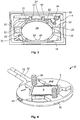
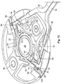
- reference numeral 2 identifies a base 2 which is an injection molded unitary disk shaped element defining, on its back side, a receptacle 4 adapted to receive a printed circuit board (PCB) 6 supporting and electrically connecting a light emitting diode (LED) 8 for defining a light emitting diode package 10.
- the PCB 6 has two distinct pads 12, 14 provided on a surface supporting the LED 8.
- the receptacle 4 has a rectangular recess 16 configured to receive the LED package 10 with limited play so that the PCB 6 is centered within the rectangular recess 16 as further exemplified in Figure 9 .
- clamping elements 18 integrally molded with the base are provided which are adapted to be elastically compressed and cooperate with the PCB 6 for holding the within the rectangular recess 16.
- the inner side faces of the receptacle 4, extending perpendicular to the clamping elements 13, are projected by space elements 20.
- the PCB 6 is supported by ridges 22 providing a rather limited support for the PCB 6.
- the clamping elements 18 are also provided with clamping ridges 24. Accordingly, the PCB 6 is essentially received with circumferential distance to the inner side faces of the rectangular recess 16 and a bottom face 26 of the receptacle 4 surrounding an opening 28 adapted to receive the LED 8.
- the clamping elements 18 are to clamp the PCB 6 sideways in the course of the assembly. After the assembly, PCB 6 is arranged level with the bottom face of the base 2.
- the base 2 has a radial slot 40 for each contact element 30.
- the radial slot 40 extends radially inwardly from the outer circumferential surface of the base 2.
- the radial slot 40 is adapted to receive one of the contact elements 30.
- a radial bore 42 is provided for receiving one of the cables 32.
- the respective radial bore 42 likewise opens to the circumferential surface of the base 2.
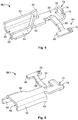
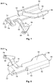
- the contact elements 30 depicted in Figures 5 - 8 have essentially the same configuration. Both contact elements 30 are made of sheet metal by cutting and bending the sheet material.
- a contact element base 50 remains as a planar basis from which outer and inner lateral walls 52, 54 project in an upper direction for defining a receiving section 56 for the cable 32.
- the inner lateral wall section 54 projects beyond the contact element base 50 to define a locking projection 58 extending parallel to the inner and outer lateral walls 52, 54.
- the other cut-free end of the inner lateral wall 54 is bent inwardly to define a resilient arm 60 arranged with distance above the contact element base 50 to define a gap suitable adapted to receive the strand 34 for passing the same between the surface of the contact element base 50 and the resilient arm 60.
- a distal end of the outer lateral wall 52 projects a plane defined by end faces of the outer and inner lateral walls 52, 54 to define an oblique pressing surface 62.
- the highest point of this oblique pressing surface 62 is provided at the distal end of a bent rim providing the outer lateral wall 52 and a distal prolongation of thereof, which distal prolongation defines the oblique pressing surface 62.
- a hammer head shaped contact section 64 projects the contact element base 50, which hammer head shaped contact section 64 comprises a straight base section 66 extending perpendicular to the lateral walls 52, 54 and a transverse section 68.
- this transverse section 68 is arranged perpendicular to the straight base section 66.
- an angle ⁇ between the straight base section 66 and the transverse section 68 is approximately 50°.
- the straight base section 66 is bent upwardly to project above a plane defined by the contact element base 50.
- the sheet metal piece defining the transverse section 68 extends parallel to the extension of the contact element base 50.
- the transverse section 68 is provided with a dimple 70.
- the transverse section 68 with the dimple 70 defines a contact lug adapted to elastically cooperate with one of the pads 12, 14 for electrically contacting the contact element 30 with this pad 12, 14.
- a guide rim 72 is provided at a distal end of the contact element.
- This guide rim 72 has a higher portion 74 and a lower portion 76.
- the contact element base 50 In longitudinal extension of the guide rim 72 and at an outer distal edge the contact element base 50 defines a downholder section 78.
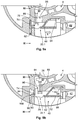
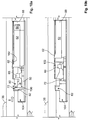
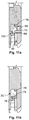
- Figs. 9a through 11b elucidate the details of one of the radial slots 40, which slot 40 is adapted to receive and hold the first embodiment of a contact element 30 depicted in Figs. 5, 6 and seen on the left hand side of Fig. 1 identified as 30.1.
- the radial slot 40 extends in a radial direction identified with arrow I, which is a radial direction and the direction for inserting the contact element 30 into the radial slot 40.
- the radial slot 40 is divided by a longish ridge 80 defining a narrow guide slot 82 adapted to receive the guide rim 72 and to guide the movement of the contact element 30 in the radial direction I.
- a housing latch 84 In the radial direction behind the ridge 80 there is provided a housing latch 84, which is in particular visible in Figs. 9a , b.
- This housing latch 84 is adapted to receive the higher portion 74 of the guide rim 72 in the course of a movement in a second direction identified with II, which second direction II extends perpendicular to the radial direction I.
- the housing latch 84 forms part of a proximal side surface of the guide slot 82.
- the opposite distal side of the base 2 defines a distal guide slot surface identified with reference numeral 86.
- the other lateral side face of the radial slot 40 is identified with reference numeral 88. As evident from Figs. 9a, 9b , this lateral side face 88 is projected in proximal direction by a holding notch 90 adapted to receive the locking projection 58.
- the width of the radial slot 40 in particular the distance between the proximal side face 88 and the housing latch 84 is such, that the outer lateral wall 52 and the proximal end of the contact element base 50 is stopped by abutment against the proximal side face 88 when being moved in the second direction II as the higher portion 74 of the guide rim 72 has moved behind a locking projection of the housing latch 84 to prevent the contact element 30 from moving in a direction opposite to the second direction II.
- the radial extension of the radial slot 40 is such, that the base 2 defines a radial inward boundary surface 92 defining a stop for the movement of the contact element 30 in the radial direction I as the higher portion 74 is aligned with a securing receptacle 94 provided by the housing latch 84 on one end and the locking projection 58 is aligned with the holding 90 on the other end.
- the radial slot 40 communicates with a contact channel 96 adapted to receive and guide the hammer head shaped contact section 64 into the receptacle 4.
- the contact element 30 For mounting the contact element 30 within the base 2, the contact element 30 is inserted into the radial slot 40 with the hammer head shaped contact section 64 aligned with the contact channel 96. In the course of this radial movement in the radial direction I, the guide rim 74 is guided through the guide slot 82. This radial movement is terminated as the contact element 30 abuts against the stop defined by the radial inward boundary surface 92. The final insertion position obtained at this stage is depicted in Figures 9a , 10a and 11a . Then, one of the cable 32 is inserted to urge the strand 34 into the gap provided between the resilient arm 60 and the upper surface of the contact element base 50.
- the contact element 30 Due to the cooperation of the guide rim 72 with the distal guide slot surface 86, the contact element 30 is held in place. Accordingly, the strand 34 can be pressed underneath the resilient arm 60.
- the resilient arm 60 has at least one sharp undersurface cooperating with the strand 34 as a barbured hook which functionality is assisted by the bendability of the resilient arm 40. Due to this, a strand 34 once inserted into the receiving section 56 underneath the resilient arm 60 cannot be easily pulled out of the contact element 30. After the cable 72 has been secured to respective contact element 30, the cable is pulled in a direction opposite to the insertion direction of the cable 32.
- the cable 32 moves the contact element 30 in the second direction II to insert the locking projection 58 into the holding lodge 90 and the higher portion 74 into the securing receptacle 94 and thus behind a form fit projection of the housing latch 84.
- the lower portion 76 of the guide rim 72 is placed underneath a downholding projection 98 provided by the base 2.
- the downholder section 78 of the contact element base 50 is placed below a downholding slot 100 provided next to the housing latch 84 and by a radial inward portion of the ridge 80.
- the oblique pressing surface 62 is pressed against an oblique counter surface 102 extending in radial direction I from the mouth of the radial slot 40 and provided by the base 2 forming part of a roof of the radial slot 40 in the course of the movement in the second radial direction II, i.e. when being moved from Fig. 9a , 10a , 11a to 9b , 10b , 11b . Due to this, the contact element 30 finds another thorough support within the radial slot 40 and is firmly jammed in the radial slot 40.
- the LED package 10 can be mounted into the receptacle to electrically connect the pads 12, 14 with the contact lugs provided by the transverse sections 68 of each contact element 30.1; 30.2. With varying location and size of the pad, the dimple's location on the transverse section 68 within the receptacle 4 may vary to provide a determined contact point by the dimple 70 for an assigned pad of another LED package 10.
- the present invention provides a simple way of electrically connecting LED packages 10 with varying pad sizes and locations in a fairly simple and inexpensive way.
- All counter surfaces for guiding the movement of the contact element 30 when mounting the contact element 30 in the base 2 are provided by the base 2.
- This base 2 likewise provides all counter surfaces for securely and reliably fixing each contact element 30.1 or 30.2 within the base 2.
- Mounting of the contact elements 30 within the base 2 does not require extra fastening means which are to be connected to the base 2 and the assigned contact element 30.
- moving of the contact element 30 in the second direction II can be attained by inserting an adapted tool into a tool channel which is identified in Figs.
- the inventive base allows a simple connection of any kind of contact element, which may per se be adapted to make contact with a pad of a PCB.
- the contact element does not necessarily have to comprise a hammer head shaped contact section.
- the contact lug of the contact element may be provided in an appropriate position within the base by properly cutting and/or bending the sheet material forming the contact element.
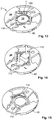
- Figures 13 to 15 show an alternate embodiment in which the LED package 10, specifically the printed circuit board 6 is adhered to the base 2 by an adhesive.
- This adhesive is provided by an adhesive tape 110 depicted in Fig. 14 and comprising two opposite surfaces which are both adhesive, wherein a lower adhesive surface is attached to the base 2 and an upper adhesive surface 112 as the second adhesive surface is fixed to the LED package 10.
- the adhesive tape 110 is provided with protective liners 114 on both surfaces and cut as a triangle adapted to match with a corner section 116 provided by the base 2 (compare Fig. 13 ).
- the liner 114 is cut as a pentagon (composed of a triangle and a square) and thus has a larger surface than the adhesive tape 116.
- the liner 114 projects into the opening 28 when being fixed with the lower first adhesive surface to the corner section 116.
- FIG. 14 shows the constitution in which both adhesive tapes 110 are adhered with their first adhesive surface to the base 2.
- the liners 116 are removed to expose the second adhesive surface 112 within the receptacle 10.
- the LED package 10 is adhered to the second adhesive surface 112.
- the second adhesive surface 112 is adhered to the flat PCB 6 by laying the PCT 6 onto the second adhesive surface 112 and pressing the PCT 6 against the base 2.
- the assembly depicted in further detail with reference to Figs. 13 to 15 is a simple and effective way of fixing the LED package 10 to the base 2.
Landscapes
- Engineering & Computer Science (AREA)
- General Engineering & Computer Science (AREA)
- Physics & Mathematics (AREA)
- Microelectronics & Electronic Packaging (AREA)
- Optics & Photonics (AREA)
- Led Device Packages (AREA)
- Fastening Of Light Sources Or Lamp Holders (AREA)
- Arrangement Of Elements, Cooling, Sealing, Or The Like Of Lighting Devices (AREA)
- Connecting Device With Holders (AREA)
- Coupling Device And Connection With Printed Circuit (AREA)
Claims (14)
- LED-Fassung, die einen Träger (2) umfasst, der eine Aufnahme (4) zum Aufnehmen einer LED-Leiterplatte einer Leuchtdioden-Baugruppe (LED package) aufweist, die eine an der LED-Leiterplatte montierte LED hat, wobei die Aufnahme (4) zu einer Öffnung (6) in dem Träger (2) offen ist, die so eingerichtet ist, dass sie die LED (8) an einer Vorderseite des Trägers (2) freilegt, und wobei der Träger (2) Kontaktelemente (30) trägt, die jeweils mit einem aufnehmenden Abschnitt (56), der zum Verbinden mit einem Anschlussende eines elektrischen Kabels (32) eingerichtet ist, sowie mit einer Kontaktfahne versehen sind, die so eingerichtet ist, dass sie mit einer Kontaktstelle (12, 14) der Leiterplatte elektrisch in Kontakt kommt,
dadurch gekennzeichnet, dass
die Kontaktfahne einen Kontakt-Abschnitt (64) in Form eines Hammerkopfes hat, der in der Aufnahme (4) freiliegt,
das Kontaktelement (30) formschlüssig in einem radialen Schlitz (40) aufgenommen ist, wobei sich der radiale Schlitz (40) von einer Außenumfangsfläche des Trägers (2) in einer radialen Richtung (I) auf die Aufnahme (4) zu erstreckt,
das Kontaktelement (30) einen Arretiervorsprung (58) hat, der Träger (2) eine Aufnahmekerbe (90) aufweist, die sich in einer zweiten Richtung (II) erstreckt, die im Wesentlichen senkrecht zu der radialen Richtung (I) verläuft, und dass der Arretiervorsprung (58) in dem Abschnitt endgültiger Einführung auf die Aufnahmekerbe (90) ausgerichtet ist. - LED-Fassung nach Anspruch 1, gekennzeichnet durch eine radiale Bohrung (42) in dem Träger (2), die zum Aufnehmen des Kabels (32) eingerichtet ist und sich auf den aufnehmenden Abschnitt (56) des Kontaktelementes (30) ausgerichtet erstreckt.
- LED-Fassung nach einem der vorangehenden Ansprüche, dadurch gekennzeichnet, dass das Kontaktelement (30) mit einer Pressfläche (62) versehen ist, dass der Träger (2) mit einer Gegenfläche (102) versehen ist, die den radialen Schlitz (40) teilweise bildet, und dass der radiale Schlitz (40) und das Kontaktelement (30) so eingerichtet sind, dass sie Einführung des Kontaktelementes (30) in den radialen Schlitz (40) in einer radialen Richtung ermöglichen, um zuzulassen, dass das Kontaktelement (30) durch Zusammenwirken der Pressfläche (62) mit der Gegenfläche (102) als ein Ergebnis von Bewegung des Kontaktelementes in der im Wesentlichen senkrecht zu der radialen Richtung (I) verlaufenden zweiten Richtung (II) in den radialen Schlitz (40) (102) hinein gepresst wird.
- LED-Fassung nach einem der vorangehenden Ansprüche, gekennzeichnet durch einen Führungs-Schlitz (82), der so eingerichtet ist, dass er einen Führungsrand (72) des Kontaktelementes (30) mit begrenztem Spiel in einer Richtung quer zu der Einführungsrichtung (I) in der Einführungsrichtung (I) des Kontaktelementes (30) führt, wobei der Führungs-Schlitz (82) und der Führungsrand (72) so eingerichtet sind, dass sie Bewegung des Kontaktelementes (30) in der zweiten Richtung (II) in einer Position endgültiger Einführung ermöglichen, in der das Kontaktelement (30) mit einem Anschlag (92) zusammenwirkt, der von dem Träger (2) gebildet wird.
- LED-Fassung nach einem der vorangehenden Ansprüche, dadurch gekennzeichnet, dass der Träger (2) eine elastische Lasche (84) umfasst und dass das Kontaktelement (30) einen Arretier-Abschnitt (74) umfasst, der so eingerichtet ist, dass er mit der elastischen Lasche (84) zusammenwirkt, um das Kontaktelement (30) in der montierten Position des Kontaktelementes (30) formschlüssig zu fixieren.
- LED-Fassung nach den Ansprüchen 4 und 5, dadurch gekennzeichnet, dass die elastische Lasche (84) eine Fixier-Aufnahme (94) aufweist, die zu dem Führungs-Schlitz (82) hin offen ist, und dass der Arretier-Abschnitt (74) in der Richtung endgültiger Einführung auf die Fixier-Aufnahme (94) ausgerichtet ist.
- LED-Fassung nach Anspruch 5, dadurch gekennzeichnet, dass das Kontaktelement (30) wenigstens einen Niederhalte-Abschnitt (76, 78) hat und dass der Träger (2) wenigstens einen Niederhalte-Schlitz (100) hat, der den Niederhalte-Abschnitt (76, 78) in der montierten Position des Kontaktelementes (30) aufnimmt.
- LED-Fassung nach einem der vorangehenden Ansprüche , dadurch gekennzeichnet, dass die LED-Baugruppe (10) mit einem Klebeband (110) an dem Träger (2) angebracht ist.
- Träger (2) einer LED-Fassung, der eine Aufnahme (4) zum Aufnehmen einer LED-Leiterplatte einer Leuchtdioden-Baugruppe (LED package) aufweist, die eine an der LED-Leiterplatte (6) montierte LED (8) sowie eine Öffnung (28) hat, die so eingerichtet ist, dass sie die LED (8) an einer Vorderseite (8) des Trägers (2) freilegt, und wobei der Träger (2) so eingerichtet ist, dass er Kontaktelemente (30.1; 30.2) trägt, die jeweils mit einer Kontaktfahne (64) versehen sind, die so eingerichtet ist, dass sie mit einer Kontaktstelle (12, 14) der Leiterplatte (6) elektrisch in Kontakt kommt, wobei der Träger (2) ein aus einem Stück bestehendes Spritzgussteil ist, das über eine Einrichtung (84, 90, 102) verfügt, die zum sicheren Verbinden des Kontaktelementes (30) mit dem Träger (2) eingerichtet ist, und wobei
der Träger (2) wenigstens einen radialen Schlitz (40) umfasst, der sich in einer radialen Richtung (I) auf die Aufnahme (4) zu erstreckt, wobei der radiale Schlitz (40) zum Aufnehmen wenigstens eines der Kontaktelemente (30.1; 30.2) eingerichtet ist, gekennzeichnet durch
eine geneigte Gegenfläche (102), die teilweise den radialen Schlitz (40) bildet und sich in der radialen Richtung (I) erstreckt, wobei die geneigte Gegenfläche (102) in einer zweiten Richtung (II) geneigt ist und sich die zweite Richtung (II) im Wesentlichen senkrecht zu der radialen Richtung (I) erstreckt. - Träger (2) nach Anspruch 9, dadurch gekennzeichnet, dass der radiale Schlitz (40) einen Führungs-Schlitz (82) aufweist, der zum Aufnehmen eines Führungsrandes (72) eines Kontaktelementes (30) eingerichtet ist und sich in der radialen Richtung (I) auf die Aufnahme (4) zu erstreckt.
- Träger (2) nach Anspruch 10, gekennzeichnet durch eine elastische Lasche (84), die im Inneren des radialen Schlitzes (40) vorhanden ist und eine Fixier-Aufnahme (94) aufweist, die zum formschlüssigen Aufnehmen eines Abschnitts (74) des Kontaktelementes (30) eingerichtet ist, wobei die Fixier-Aufnahme (94) zu dem Führungs-Schlitz (82) offen ist und im Inneren eines Stegs (80) ausgebildet ist, der sich in radialer Richtung (I) erstreckt und den Führungs-Schlitz (82) im Inneren des radialen Schlitzes (40) bildet.
- Träger (2) nach einem der Ansprüche 9 bis 11, gekennzeichnet durch eine Aufnahmekerbe (90), die sich in der zweiten Richtung (II) erstreckt und in dem radialen Schlitz (82) endet.
- Träger (2) nach einem der Ansprüche 9 bis 12, gekennzeichnet durch ein Klebeband (110), das zum Befestigen der LED-Baugruppe (10) an dem Träger (2) eingerichtet ist.
- Träger (2) nach Anspruch 13, dadurch gekennzeichnet, dass das Klebeband (110) eine erste Klebefläche, die an dem Träger (2) befestigt ist, sowie eine zweite Klebefläche (112) hat, die zum Befestigen an der LED-Baugruppe (10) eingerichtet ist und mit einer Schutzverkleidung (114) abgedeckt ist.
Applications Claiming Priority (2)
| Application Number | Priority Date | Filing Date | Title |
|---|---|---|---|
| EP15200137.6A EP3181987A1 (de) | 2015-12-15 | 2015-12-15 | Led-fassung zur aufnahme einer cob-led und basis für eine solche led-fassung |
| PCT/EP2016/055461 WO2017102100A1 (en) | 2015-12-15 | 2016-03-14 | Led socket for receiving a cob-led and base for such led socket |
Publications (2)
| Publication Number | Publication Date |
|---|---|
| EP3390894A1 EP3390894A1 (de) | 2018-10-24 |
| EP3390894B1 true EP3390894B1 (de) | 2020-09-02 |
Family
ID=54979416
Family Applications (2)
| Application Number | Title | Priority Date | Filing Date |
|---|---|---|---|
| EP15200137.6A Withdrawn EP3181987A1 (de) | 2015-12-15 | 2015-12-15 | Led-fassung zur aufnahme einer cob-led und basis für eine solche led-fassung |
| EP16711193.9A Active EP3390894B1 (de) | 2015-12-15 | 2016-03-14 | Led-fassung zur aufnahme einer cob-led und basis für eine solche led-fassung |
Family Applications Before (1)
| Application Number | Title | Priority Date | Filing Date |
|---|---|---|---|
| EP15200137.6A Withdrawn EP3181987A1 (de) | 2015-12-15 | 2015-12-15 | Led-fassung zur aufnahme einer cob-led und basis für eine solche led-fassung |
Country Status (5)
| Country | Link |
|---|---|
| US (1) | US10429048B2 (de) |
| EP (2) | EP3181987A1 (de) |
| JP (1) | JP6667660B2 (de) |
| CN (1) | CN108368976B (de) |
| WO (1) | WO2017102100A1 (de) |
Families Citing this family (6)
| Publication number | Priority date | Publication date | Assignee | Title |
|---|---|---|---|---|
| DE102018114075B4 (de) * | 2017-06-13 | 2025-04-30 | Electro Terminal GmbH & Co. KG | LED-Modul-Baugruppe |
| US11378259B2 (en) | 2018-12-19 | 2022-07-05 | Nichia Corporation | Light-emitting module |
| CA192472S (en) * | 2020-01-14 | 2022-04-14 | Structure Shims Inc | Round manhole extension form |
| CA192473S (en) * | 2020-01-14 | 2022-04-25 | Structure Shims Inc | Square storm sewer extension form |
| USD1074044S1 (en) * | 2022-06-21 | 2025-05-06 | Archangel Device Llc | Base for a lighting device |
| EP4713617A1 (de) * | 2023-05-18 | 2026-03-25 | Signify Holding B.V. | Cob-halter |
Family Cites Families (19)
| Publication number | Priority date | Publication date | Assignee | Title |
|---|---|---|---|---|
| GB2247363B (en) * | 1990-07-26 | 1995-01-18 | Nce Electrical | Electrical adaptor assembly |
| US8608359B2 (en) * | 2008-01-30 | 2013-12-17 | Kyocera Corporation | Mobile terminal having a light source and a light reflector within the mobile terminal to illuminate the mobile terminal |
| TWM409543U (en) * | 2010-01-13 | 2011-08-11 | Molex Inc | Holder assembly |
| JP2012119523A (ja) * | 2010-12-01 | 2012-06-21 | Stanley Electric Co Ltd | 静電気対策を施した電子装置 |
| US9146027B2 (en) * | 2011-04-08 | 2015-09-29 | Ideal Industries, Inc. | Device for holding a source of LED light |
| CN102927456B (zh) * | 2011-08-09 | 2016-08-03 | 欧司朗股份有限公司 | Led发光组件和具有该led发光组件的led改型灯 |
| JP5965120B2 (ja) * | 2011-09-13 | 2016-08-03 | タイコエレクトロニクスジャパン合同会社 | Ledソケット |
| US9423119B2 (en) * | 2011-09-26 | 2016-08-23 | Ideal Industries, Inc. | Device for securing a source of LED light to a heat sink surface |
| FI123715B (en) * | 2011-12-22 | 2013-09-30 | Upm Kymmene Corp | Composition for embedded microbial culture |
| US9170002B2 (en) * | 2012-01-05 | 2015-10-27 | Molex, Llc | Holder and LED module using same |
| US8568001B2 (en) | 2012-02-03 | 2013-10-29 | Tyco Electronics Corporation | LED socket assembly |
| US9494303B2 (en) * | 2012-03-02 | 2016-11-15 | Molex, Llc | LED module and holder with terminal well |
| EP2648289B1 (de) * | 2012-04-02 | 2018-03-07 | TE Connectivity Nederland B.V. | Kontaktelement, Klemmelement, Basis und Anordnung zum Halten und Kontaktieren einer LED |
| CN203202944U (zh) * | 2013-05-03 | 2013-09-18 | 莫列斯公司 | 发光装置及其安装座 |
| TWI659179B (zh) * | 2013-08-09 | 2019-05-11 | 摩勒克斯公司 | 固持座組件 |
| TWM472152U (zh) * | 2013-09-05 | 2014-02-11 | Molex Taiwan Ltd | 安裝座與照明裝置 |
| JP6285035B2 (ja) * | 2014-01-02 | 2018-02-28 | ティーイー コネクティビティ ネーデルランド ビーヴイTE Connectivity Nederland BV | Ledソケットアセンブリ |
| US10436423B2 (en) * | 2014-01-10 | 2019-10-08 | Molex, Llc | Insert and LED holder assembly using same |
| CN104051922B (zh) * | 2014-06-16 | 2015-12-02 | 东莞市奕东电子有限公司 | 一种免焊led cob光源连接扣件及其连接方法 |
-
2015
- 2015-12-15 EP EP15200137.6A patent/EP3181987A1/de not_active Withdrawn
-
2016
- 2016-03-14 WO PCT/EP2016/055461 patent/WO2017102100A1/en not_active Ceased
- 2016-03-14 EP EP16711193.9A patent/EP3390894B1/de active Active
- 2016-03-14 JP JP2018549390A patent/JP6667660B2/ja active Active
- 2016-03-14 CN CN201680072833.6A patent/CN108368976B/zh active Active
-
2018
- 2018-06-15 US US16/009,796 patent/US10429048B2/en active Active
Non-Patent Citations (1)
| Title |
|---|
| None * |
Also Published As
| Publication number | Publication date |
|---|---|
| JP6667660B2 (ja) | 2020-03-18 |
| CN108368976A (zh) | 2018-08-03 |
| WO2017102100A1 (en) | 2017-06-22 |
| US10429048B2 (en) | 2019-10-01 |
| CN108368976B (zh) | 2020-10-16 |
| US20180292075A1 (en) | 2018-10-11 |
| JP2019502247A (ja) | 2019-01-24 |
| EP3390894A1 (de) | 2018-10-24 |
| EP3181987A1 (de) | 2017-06-21 |
Similar Documents
| Publication | Publication Date | Title |
|---|---|---|
| EP3390894A1 (de) | Led-fassung zur aufnahme einer cob-led und basis für solch eine led-fassung | |
| EP3149809B1 (de) | Elektrischer verbinder zur verwendung mit bestückten leiterplatten | |
| US8834194B2 (en) | LED socket having a housing with a securing member and a LED module receiving portion | |
| US9166319B2 (en) | Flexible circuit board connector | |
| US9482423B2 (en) | Device for securing a source of LED light to a heat sink surface | |
| US9160086B2 (en) | Electrical connectors for use with printed circuit boards | |
| EP2564474B1 (de) | Led-fassungsanordnung | |
| KR101450737B1 (ko) | 커넥터 | |
| US9484639B1 (en) | Openable wire-mounting connector | |
| US20140268887A1 (en) | Device for securing a source of led light to a heat sink surface | |
| US9172162B2 (en) | Circuit board connector | |
| US20140268886A1 (en) | Device for securing a source of led light to a heat sink surface | |
| EP3107157A1 (de) | Wandhalterungskomponente und drahtklemmverbinder dafür | |
| WO2016175101A1 (ja) | 照明装置 | |
| TWI506899B (zh) | 連接器及照明裝置 | |
| JP7591862B2 (ja) | 灯具、照明装置及び電線保持具 | |
| JP2014093182A (ja) | ランプホルダ | |
| WO2020182800A1 (en) | A holder for snap-fitting a thermal fuse to an electronic component | |
| JP2001345131A (ja) | 電源端子台及び照明器具 |
Legal Events
| Date | Code | Title | Description |
|---|---|---|---|
| STAA | Information on the status of an ep patent application or granted ep patent |
Free format text: STATUS: THE INTERNATIONAL PUBLICATION HAS BEEN MADE |
|
| PUAI | Public reference made under article 153(3) epc to a published international application that has entered the european phase |
Free format text: ORIGINAL CODE: 0009012 |
|
| STAA | Information on the status of an ep patent application or granted ep patent |
Free format text: STATUS: REQUEST FOR EXAMINATION WAS MADE |
|
| 17P | Request for examination filed |
Effective date: 20180710 |
|
| AK | Designated contracting states |
Kind code of ref document: A1 Designated state(s): AL AT BE BG CH CY CZ DE DK EE ES FI FR GB GR HR HU IE IS IT LI LT LU LV MC MK MT NL NO PL PT RO RS SE SI SK SM TR |
|
| AX | Request for extension of the european patent |
Extension state: BA ME |
|
| DAV | Request for validation of the european patent (deleted) | ||
| DAX | Request for extension of the european patent (deleted) | ||
| STAA | Information on the status of an ep patent application or granted ep patent |
Free format text: STATUS: EXAMINATION IS IN PROGRESS |
|
| 17Q | First examination report despatched |
Effective date: 20190618 |
|
| REG | Reference to a national code |
Ref country code: DE Ref legal event code: R079 Ref document number: 602016043142 Country of ref document: DE Free format text: PREVIOUS MAIN CLASS: F21K0099000000 Ipc: F21K0009000000 |
|
| RIC1 | Information provided on ipc code assigned before grant |
Ipc: H01R 4/48 20060101ALI20200117BHEP Ipc: F21V 23/06 20060101ALI20200117BHEP Ipc: F21K 9/00 20160101AFI20200117BHEP Ipc: F21Y 101/00 20160101ALN20200117BHEP Ipc: F21V 19/00 20060101ALI20200117BHEP Ipc: H01R 12/53 20110101ALI20200117BHEP |
|
| RIC1 | Information provided on ipc code assigned before grant |
Ipc: F21V 19/00 20060101ALI20200225BHEP Ipc: F21K 9/00 20160101AFI20200225BHEP Ipc: F21Y 101/00 20160101ALN20200225BHEP Ipc: F21V 23/06 20060101ALI20200225BHEP Ipc: H01R 4/48 20060101ALI20200225BHEP Ipc: H01R 12/53 20110101ALI20200225BHEP |
|
| GRAP | Despatch of communication of intention to grant a patent |
Free format text: ORIGINAL CODE: EPIDOSNIGR1 |
|
| STAA | Information on the status of an ep patent application or granted ep patent |
Free format text: STATUS: GRANT OF PATENT IS INTENDED |
|
| INTG | Intention to grant announced |
Effective date: 20200403 |
|
| GRAS | Grant fee paid |
Free format text: ORIGINAL CODE: EPIDOSNIGR3 |
|
| GRAA | (expected) grant |
Free format text: ORIGINAL CODE: 0009210 |
|
| STAA | Information on the status of an ep patent application or granted ep patent |
Free format text: STATUS: THE PATENT HAS BEEN GRANTED |
|
| AK | Designated contracting states |
Kind code of ref document: B1 Designated state(s): AL AT BE BG CH CY CZ DE DK EE ES FI FR GB GR HR HU IE IS IT LI LT LU LV MC MK MT NL NO PL PT RO RS SE SI SK SM TR |
|
| REG | Reference to a national code |
Ref country code: GB Ref legal event code: FG4D |
|
| REG | Reference to a national code |
Ref country code: AT Ref legal event code: REF Ref document number: 1309229 Country of ref document: AT Kind code of ref document: T Effective date: 20200915 Ref country code: CH Ref legal event code: EP |
|
| REG | Reference to a national code |
Ref country code: DE Ref legal event code: R096 Ref document number: 602016043142 Country of ref document: DE |
|
| REG | Reference to a national code |
Ref country code: IE Ref legal event code: FG4D |
|
| REG | Reference to a national code |
Ref country code: LT Ref legal event code: MG4D |
|
| PG25 | Lapsed in a contracting state [announced via postgrant information from national office to epo] |
Ref country code: GR Free format text: LAPSE BECAUSE OF FAILURE TO SUBMIT A TRANSLATION OF THE DESCRIPTION OR TO PAY THE FEE WITHIN THE PRESCRIBED TIME-LIMIT Effective date: 20201203 Ref country code: SE Free format text: LAPSE BECAUSE OF FAILURE TO SUBMIT A TRANSLATION OF THE DESCRIPTION OR TO PAY THE FEE WITHIN THE PRESCRIBED TIME-LIMIT Effective date: 20200902 Ref country code: NO Free format text: LAPSE BECAUSE OF FAILURE TO SUBMIT A TRANSLATION OF THE DESCRIPTION OR TO PAY THE FEE WITHIN THE PRESCRIBED TIME-LIMIT Effective date: 20201202 Ref country code: BG Free format text: LAPSE BECAUSE OF FAILURE TO SUBMIT A TRANSLATION OF THE DESCRIPTION OR TO PAY THE FEE WITHIN THE PRESCRIBED TIME-LIMIT Effective date: 20201202 Ref country code: LT Free format text: LAPSE BECAUSE OF FAILURE TO SUBMIT A TRANSLATION OF THE DESCRIPTION OR TO PAY THE FEE WITHIN THE PRESCRIBED TIME-LIMIT Effective date: 20200902 Ref country code: HR Free format text: LAPSE BECAUSE OF FAILURE TO SUBMIT A TRANSLATION OF THE DESCRIPTION OR TO PAY THE FEE WITHIN THE PRESCRIBED TIME-LIMIT Effective date: 20200902 Ref country code: FI Free format text: LAPSE BECAUSE OF FAILURE TO SUBMIT A TRANSLATION OF THE DESCRIPTION OR TO PAY THE FEE WITHIN THE PRESCRIBED TIME-LIMIT Effective date: 20200902 |
|
| REG | Reference to a national code |
Ref country code: NL Ref legal event code: MP Effective date: 20200902 |
|
| REG | Reference to a national code |
Ref country code: AT Ref legal event code: MK05 Ref document number: 1309229 Country of ref document: AT Kind code of ref document: T Effective date: 20200902 |
|
| PG25 | Lapsed in a contracting state [announced via postgrant information from national office to epo] |
Ref country code: PL Free format text: LAPSE BECAUSE OF FAILURE TO SUBMIT A TRANSLATION OF THE DESCRIPTION OR TO PAY THE FEE WITHIN THE PRESCRIBED TIME-LIMIT Effective date: 20200902 Ref country code: RS Free format text: LAPSE BECAUSE OF FAILURE TO SUBMIT A TRANSLATION OF THE DESCRIPTION OR TO PAY THE FEE WITHIN THE PRESCRIBED TIME-LIMIT Effective date: 20200902 Ref country code: LV Free format text: LAPSE BECAUSE OF FAILURE TO SUBMIT A TRANSLATION OF THE DESCRIPTION OR TO PAY THE FEE WITHIN THE PRESCRIBED TIME-LIMIT Effective date: 20200902 |
|
| PG25 | Lapsed in a contracting state [announced via postgrant information from national office to epo] |
Ref country code: EE Free format text: LAPSE BECAUSE OF FAILURE TO SUBMIT A TRANSLATION OF THE DESCRIPTION OR TO PAY THE FEE WITHIN THE PRESCRIBED TIME-LIMIT Effective date: 20200902 Ref country code: PT Free format text: LAPSE BECAUSE OF FAILURE TO SUBMIT A TRANSLATION OF THE DESCRIPTION OR TO PAY THE FEE WITHIN THE PRESCRIBED TIME-LIMIT Effective date: 20210104 Ref country code: SM Free format text: LAPSE BECAUSE OF FAILURE TO SUBMIT A TRANSLATION OF THE DESCRIPTION OR TO PAY THE FEE WITHIN THE PRESCRIBED TIME-LIMIT Effective date: 20200902 Ref country code: RO Free format text: LAPSE BECAUSE OF FAILURE TO SUBMIT A TRANSLATION OF THE DESCRIPTION OR TO PAY THE FEE WITHIN THE PRESCRIBED TIME-LIMIT Effective date: 20200902 Ref country code: CZ Free format text: LAPSE BECAUSE OF FAILURE TO SUBMIT A TRANSLATION OF THE DESCRIPTION OR TO PAY THE FEE WITHIN THE PRESCRIBED TIME-LIMIT Effective date: 20200902 |
|
| PG25 | Lapsed in a contracting state [announced via postgrant information from national office to epo] |
Ref country code: IS Free format text: LAPSE BECAUSE OF FAILURE TO SUBMIT A TRANSLATION OF THE DESCRIPTION OR TO PAY THE FEE WITHIN THE PRESCRIBED TIME-LIMIT Effective date: 20210102 Ref country code: AL Free format text: LAPSE BECAUSE OF FAILURE TO SUBMIT A TRANSLATION OF THE DESCRIPTION OR TO PAY THE FEE WITHIN THE PRESCRIBED TIME-LIMIT Effective date: 20200902 Ref country code: AT Free format text: LAPSE BECAUSE OF FAILURE TO SUBMIT A TRANSLATION OF THE DESCRIPTION OR TO PAY THE FEE WITHIN THE PRESCRIBED TIME-LIMIT Effective date: 20200902 Ref country code: ES Free format text: LAPSE BECAUSE OF FAILURE TO SUBMIT A TRANSLATION OF THE DESCRIPTION OR TO PAY THE FEE WITHIN THE PRESCRIBED TIME-LIMIT Effective date: 20200902 |
|
| REG | Reference to a national code |
Ref country code: DE Ref legal event code: R097 Ref document number: 602016043142 Country of ref document: DE |
|
| PG25 | Lapsed in a contracting state [announced via postgrant information from national office to epo] |
Ref country code: SK Free format text: LAPSE BECAUSE OF FAILURE TO SUBMIT A TRANSLATION OF THE DESCRIPTION OR TO PAY THE FEE WITHIN THE PRESCRIBED TIME-LIMIT Effective date: 20200902 |
|
| PLBE | No opposition filed within time limit |
Free format text: ORIGINAL CODE: 0009261 |
|
| STAA | Information on the status of an ep patent application or granted ep patent |
Free format text: STATUS: NO OPPOSITION FILED WITHIN TIME LIMIT |
|
| 26N | No opposition filed |
Effective date: 20210603 |
|
| PG25 | Lapsed in a contracting state [announced via postgrant information from national office to epo] |
Ref country code: DK Free format text: LAPSE BECAUSE OF FAILURE TO SUBMIT A TRANSLATION OF THE DESCRIPTION OR TO PAY THE FEE WITHIN THE PRESCRIBED TIME-LIMIT Effective date: 20200902 Ref country code: SI Free format text: LAPSE BECAUSE OF FAILURE TO SUBMIT A TRANSLATION OF THE DESCRIPTION OR TO PAY THE FEE WITHIN THE PRESCRIBED TIME-LIMIT Effective date: 20200902 |
|
| PG25 | Lapsed in a contracting state [announced via postgrant information from national office to epo] |
Ref country code: IT Free format text: LAPSE BECAUSE OF FAILURE TO SUBMIT A TRANSLATION OF THE DESCRIPTION OR TO PAY THE FEE WITHIN THE PRESCRIBED TIME-LIMIT Effective date: 20200902 Ref country code: MC Free format text: LAPSE BECAUSE OF FAILURE TO SUBMIT A TRANSLATION OF THE DESCRIPTION OR TO PAY THE FEE WITHIN THE PRESCRIBED TIME-LIMIT Effective date: 20200902 |
|
| REG | Reference to a national code |
Ref country code: CH Ref legal event code: PL |
|
| REG | Reference to a national code |
Ref country code: BE Ref legal event code: MM Effective date: 20210331 |
|
| PG25 | Lapsed in a contracting state [announced via postgrant information from national office to epo] |
Ref country code: IE Free format text: LAPSE BECAUSE OF NON-PAYMENT OF DUE FEES Effective date: 20210314 Ref country code: CH Free format text: LAPSE BECAUSE OF NON-PAYMENT OF DUE FEES Effective date: 20210331 Ref country code: LU Free format text: LAPSE BECAUSE OF NON-PAYMENT OF DUE FEES Effective date: 20210314 Ref country code: LI Free format text: LAPSE BECAUSE OF NON-PAYMENT OF DUE FEES Effective date: 20210331 |
|
| PG25 | Lapsed in a contracting state [announced via postgrant information from national office to epo] |
Ref country code: BE Free format text: LAPSE BECAUSE OF NON-PAYMENT OF DUE FEES Effective date: 20210331 |
|
| PG25 | Lapsed in a contracting state [announced via postgrant information from national office to epo] |
Ref country code: NL Free format text: LAPSE BECAUSE OF NON-PAYMENT OF DUE FEES Effective date: 20200923 Ref country code: CY Free format text: LAPSE BECAUSE OF FAILURE TO SUBMIT A TRANSLATION OF THE DESCRIPTION OR TO PAY THE FEE WITHIN THE PRESCRIBED TIME-LIMIT Effective date: 20200902 |
|
| PG25 | Lapsed in a contracting state [announced via postgrant information from national office to epo] |
Ref country code: HU Free format text: LAPSE BECAUSE OF FAILURE TO SUBMIT A TRANSLATION OF THE DESCRIPTION OR TO PAY THE FEE WITHIN THE PRESCRIBED TIME-LIMIT; INVALID AB INITIO Effective date: 20160314 |
|
| PG25 | Lapsed in a contracting state [announced via postgrant information from national office to epo] |
Ref country code: MK Free format text: LAPSE BECAUSE OF FAILURE TO SUBMIT A TRANSLATION OF THE DESCRIPTION OR TO PAY THE FEE WITHIN THE PRESCRIBED TIME-LIMIT Effective date: 20200902 |
|
| PGFP | Annual fee paid to national office [announced via postgrant information from national office to epo] |
Ref country code: GB Payment date: 20240108 Year of fee payment: 9 |
|
| PGFP | Annual fee paid to national office [announced via postgrant information from national office to epo] |
Ref country code: FR Payment date: 20240103 Year of fee payment: 9 |
|
| PG25 | Lapsed in a contracting state [announced via postgrant information from national office to epo] |
Ref country code: TR Free format text: LAPSE BECAUSE OF FAILURE TO SUBMIT A TRANSLATION OF THE DESCRIPTION OR TO PAY THE FEE WITHIN THE PRESCRIBED TIME-LIMIT Effective date: 20200902 |
|
| PG25 | Lapsed in a contracting state [announced via postgrant information from national office to epo] |
Ref country code: MT Free format text: LAPSE BECAUSE OF FAILURE TO SUBMIT A TRANSLATION OF THE DESCRIPTION OR TO PAY THE FEE WITHIN THE PRESCRIBED TIME-LIMIT Effective date: 20200902 |
|
| GBPC | Gb: european patent ceased through non-payment of renewal fee |
Effective date: 20250314 |
|
| PG25 | Lapsed in a contracting state [announced via postgrant information from national office to epo] |
Ref country code: GB Free format text: LAPSE BECAUSE OF NON-PAYMENT OF DUE FEES Effective date: 20250314 |
|
| PG25 | Lapsed in a contracting state [announced via postgrant information from national office to epo] |
Ref country code: FR Free format text: LAPSE BECAUSE OF NON-PAYMENT OF DUE FEES Effective date: 20250331 |
|
| PGFP | Annual fee paid to national office [announced via postgrant information from national office to epo] |
Ref country code: DE Payment date: 20260102 Year of fee payment: 11 |