EP3389007B1 - Substratbildverarbeitungsvorrichtung und substratbildverarbeitungsverfahren - Google Patents
Substratbildverarbeitungsvorrichtung und substratbildverarbeitungsverfahren Download PDFInfo
- Publication number
- EP3389007B1 EP3389007B1 EP15910178.1A EP15910178A EP3389007B1 EP 3389007 B1 EP3389007 B1 EP 3389007B1 EP 15910178 A EP15910178 A EP 15910178A EP 3389007 B1 EP3389007 B1 EP 3389007B1
- Authority
- EP
- European Patent Office
- Prior art keywords
- template
- board
- image data
- image processing
- mark
- Prior art date
- Legal status (The legal status is an assumption and is not a legal conclusion. Google has not performed a legal analysis and makes no representation as to the accuracy of the status listed.)
- Active
Links
Images


Classifications
-
- G—PHYSICS
- G06—COMPUTING OR CALCULATING; COUNTING
- G06T—IMAGE DATA PROCESSING OR GENERATION, IN GENERAL
- G06T1/00—General purpose image data processing
-
- G—PHYSICS
- G06—COMPUTING OR CALCULATING; COUNTING
- G06T—IMAGE DATA PROCESSING OR GENERATION, IN GENERAL
- G06T7/00—Image analysis
- G06T7/70—Determining position or orientation of objects or cameras
- G06T7/73—Determining position or orientation of objects or cameras using feature-based methods
- G06T7/74—Determining position or orientation of objects or cameras using feature-based methods involving reference images or patches
-
- G—PHYSICS
- G06—COMPUTING OR CALCULATING; COUNTING
- G06T—IMAGE DATA PROCESSING OR GENERATION, IN GENERAL
- G06T7/00—Image analysis
-
- H—ELECTRICITY
- H05—ELECTRIC TECHNIQUES NOT OTHERWISE PROVIDED FOR
- H05K—PRINTED CIRCUITS; CASINGS OR CONSTRUCTIONAL DETAILS OF ELECTRIC APPARATUS; MANUFACTURE OF ASSEMBLAGES OF ELECTRICAL COMPONENTS
- H05K13/00—Apparatus or processes specially adapted for manufacturing or adjusting assemblages of electric components
- H05K13/04—Mounting of components, e.g. of leadless components
-
- G—PHYSICS
- G06—COMPUTING OR CALCULATING; COUNTING
- G06T—IMAGE DATA PROCESSING OR GENERATION, IN GENERAL
- G06T2207/00—Indexing scheme for image analysis or image enhancement
- G06T2207/30—Subject of image; Context of image processing
- G06T2207/30108—Industrial image inspection
- G06T2207/30141—Printed circuit board [PCB]
Definitions
- the present invention relates to an image processing device and an image processing method for a board.
- Patent Document 1 discloses a configuration for recognizing a reference position of a board carried into a component mounting machine.
- a distinctive portion in the wiring pattern is detected as a fiducial marker from image data obtained by capturing an image of the wiring pattern of the board.
- a template showing the distinctive portion in the wiring pattern is used similar to a reference line having a shape conforming to the edge of the distinctive portion or a plurality of seek lines intersecting the edge.
- Patent Document 1 Patent Document 2 and Patent Document 3 provide further image processing devices according to the prior art.
- the image processing device displays the image data to the operator, and complements the detection process by receiving a setting of the reference position in the image data.
- the setting of the reference position by manual operation of the operator may include an error due to visual measurement.
- the image processing device for a board and the image processing method for a board are defined in the appended claims.
- the reference position of the board is recognized by using the second template which shows other distinguishing portions included in the first region.
- the complementary procedure using the second template can be executed, and the reference position can be recognized with higher accuracy than the case where the reference position of the board is set by the manual operation of the operator.
- the image data acquired in the initial detection process using the first template can be redirected, the processing efficiency in the image processing can be improved, and the time required for a complementary process can be shortened.
- the embodiment is an example of a configuration in which an image processing device for a board is incorporated in a component mounting machine constituting a production line for manufacturing a circuit board product such as an integrated circuit.
- the production line 1 is composed of multiple production devices that are communicably connected to a host computer 2 via a network.
- the production device includes, for example, a screen printing machine, a mounting inspection machine, a reflow furnace, and the like.
- the production device that includes the component mounting machine 10 is configured to be capable of inputting and outputting various data to and from the host computer 2 via the network.
- the host computer 2 monitors the operating state of the production line 1 and controls production devices which include the component mounting machine 10.
- the host computer 2 stores various data for controlling the component mounting machine 10.
- the various data described above includes a production plan, which includes the type and production volume of the circuit board product to be produced, a control program for operating the component mounting machine 10, and a template used for image processing.
- the host computer 2 appropriately sends various data, such as the control program, to each production device when a production process is executed at each production device.
- a plurality of component mounting machines 10 constituting the production line 1 include a board conveyance device 11, a component supply device 12, a component transfer device 13, a component camera 14, a board camera 15, and a control device 20.
- the horizontal width direction (i.e., the left-right direction in FIG. 1 ) of the component mounting machine 10 is defined as the X-axis direction
- the horizontal depth direction (i.e., the up-down direction in FIG. 1 ) of the component mounting machine 10 is defined as the Y-axis direction
- the vertical direction i.e., the front-rear direction in FIG. 1 ) perpendicular to the X-axis and the Y-axis is defined as the Z-axis direction.
- the board conveyance device 11 is composed of a belt conveyor or the like, and sequentially conveys the board 50 in the conveyance direction (i.e, the X-axis direction in the present embodiment).
- the board conveyance device 11 positions the board 50 at a predetermined position in the component mounting machine 10. After a mounting process is executed by the component mounting machine 10, the board conveyance device 11 carries the board 50 out of the component mounting machine 10.
- the component supply device 12 supplies electronic components to be mounted on the board 50 at a supply position Ps.
- the component supply device 12 has a plurality of slots arranged side by side in the X-axis direction.
- a feeder 12a is detachably set in each of the plurality of slots.
- the component supply device 12 feeds and moves, for example, a carrier tape with the feeder 12a and supplies electronic components at a retrieval portion located on the edge (i.e., the upper portion in FIG. 1 ) of the feeder 12a.
- the component transfer device 13 is configured to be movable in the X-axis direction and the Y-axis direction.
- the component transfer device 13 is arranged from the rear (i.e., the upper side in FIG. 1 ) in the depth direction of the component mounting machine 10 to the top of the component supply device 12 at the front of the component mounting machine 10.
- the component transfer device 13 is provided with a head driving device 13a, a moving table 13b, and a mounting head 13c.
- the head driving device 13a is configured so that the moving table 13b can be moved in the XY-axis direction by a linear motion mechanism.
- the mounting head 13c is clamped and fixed to the moving table 13b via a frame (not shown).
- a plurality of suction nozzles (not shown) are detachably provided on the mounting head 13c.
- the mounting head 13c supports each suction nozzle so as to be rotatable about an R-axis parallel to the Z-axis and capable of ascending and descending.
- Each suction nozzle is controlled in its elevation position and angle with respect to the mounting head 13c, and negative pressure supply state.
- Each suction nozzle draws in and holds an electronic component supplied at the retrieval portion of the feeder 12a by being supplied with negative pressure.
- the component camera 14 and the board camera 15 are digital imaging devices each having an imaging device such as a CCD (Charge Coupled Device) or a CMOS (Complementary Metal Oxide Semiconductor).
- the component camera 14 and the board camera 15 perform imaging in a range within the camera field of view based on a control signal from the communicably connected control device 20 and transmit the image data acquired by the imaging to the control device 20.
- the component camera 14 is fixed to the base of the component mounting machine 10 such that the optical axis is directed upward in the vertical direction (i.e., in the Z-axis direction) and is configured to capture an image from below the component transfer device 13. More specifically, the component camera 14 is configured to capture an image of the lower surface of the electronic component held by the suction nozzle.
- the board camera 15 is provided on the moving table 13b of the component transfer device 13 so that the optical axis is directed downward in the vertical direction (i.e., the Z-axis direction). The board camera 15 is configured to capture an image of the board 50.
- the control device 20 is mainly composed of a CPU, various types of memory, and a control circuit.
- the control device 20 controls the mounting process of the electronic component.
- the control device 20 is communicably connected to the host computer 2 via the network. As shown in FIG. 1 , the control device 20 includes a mounting control unit 21, a storage device 22, a display device 23, an input device 24, and an image processing device 30.
- the mounting control unit 21 controls the position of the mounting head 13c and operation of the suction mechanism. More specifically, the mounting control unit 21 inputs information output from a plurality of sensors provided in the component mounting machine 10 and results of various recognition processes. The mounting control unit 21 then sends a control signal to the component transfer device 13 based on the control program stored in the storage device 22, the information from the various sensors, and the result of the recognition process of the image processing device 30. As a result, the position and the rotation angle of the suction nozzle supported by the mounting head 13c are controlled.
- the storage device 22 is configured by an optical drive device such as a hard disk device, a flash memory, or the like.
- the storage device 22 stores a control program, control information, image data, temporary data of various processes performed by the image processing device 30, and the like.
- the display device 23 displays various data as images to the operator.
- the input device 24 is a device that accepts input of various data by manual operation of the operator.
- the image processing device 30 acquires image data by capturing images with the component camera 14 and the board camera 15, and executes image processing in accordance with the application.
- the image processing may include, for example, binarization of image data, filtering, hue extraction, super-resolution processing, and the like.
- the image processing device 30 executes image processing for recognizing the reference position of the board 50.
- the control device 20 corrects the position of the suction nozzle held by the mounting head 13c according to the positioning state of the board 50 based on the result of image processing for recognizing the reference position of the board 50.
- the electronic component is mounted at an appropriate position on the board 50 and the accuracy of the mounting process is improved.
- the image processing device 30 adopts a rectangular fiducial mark 55 (hereinafter, referred to as an "F-mark") as a fiducial mark.
- the image processing device 30 includes an image acquisition unit 31, a detection unit 32, a template acquisition unit 33, and a position recognition unit 35.
- the image acquisition unit 31 acquires image data 60 (see FIG. 3 ) obtained by imaging the first region M (see FIG. 2 ) that includes the F-mark 55, which is a fiducial mark disposed on the upper surface of the board 50.
- the "first region M" is a region that can be imaged by the board camera 15 that is moved relative to the board 50.
- the detection unit 32 scans the image data 60 using the first template 70 that shows the shape of the F-mark 55, which is a fiducial mark, and detects the position of the F-mark 55.
- the template used for detection such as the first template 70, is composed of a standard line having a shape corresponding to the edge of a detection target (here, the F-mark 55) or a plurality of seek lines arranged based on the shape of the edge, and is stored in the storage device 22.
- the first template 70 is composed of a plurality of seek lines 71 intersecting the edge of the F-mark 55 and a defining point 72 indicating the position of the F-mark 55 when the F-mark 55 is detected.
- the positional relationship of the first template 70 with the reference position of the board 50 is defined by the position of the defining point 72.
- the template acquisition unit 33 acquires a second template 80 that shows a distinctive portion 53 of the board 50 located outside the F-mark 55 in the first region M (see FIG. 6 ).
- the image processing device 30 needs to recognize the reference position of the board 50 by another method. In this case, the image processing device 30 executes a complementary process that complements the detection process.
- the second template 80 used in the above-described complementary process shows a distinctive portion 53 of the board 50 surrounding the F-mark 55 and at a position within the first region M.
- the distinctive portion 53 of the board 50 consists of a shape, a pattern, a color, or a combination thereof formed by a wiring pattern on the upper surface of the board, printed solder, a mounted electronic component, or the like.
- the distinctive portion 53 of the board 50 is a characteristically-shaped wiring pattern formed on the upper surface of the board 50.
- the wiring pattern of the board 50 is composed of lands 51, which are applied by printing solder or the like and electrically connected to the terminals of an electronic component, and wiring portions 52, which connect the lands 51 to each other. More specifically, the distinctive portion 53 of the board 50 is constituted by a plurality of lands 51 having a rectangular-shaped positional relationship.
- the second template 80 is composed of a plurality of standard lines 81 and a defining point 82.
- the plurality of standard lines 81 indicate the edges and positional relationship of the plurality of lands 51.
- the defining point 82 indicates the position of the F-mark 55 which is not detected when the distinctive portion 53 of the board 50 is detected. That is, similarly to the first template 70, the positional relationship of the second template 80 with the reference position of the board 50 is defined by the position of the defining point 82. Furthermore, in FIG. 6 , the F-mark 55 is indicated by a broken line.
- the second template 80 may be appropriately generated in the complementary process. Details of the method for acquiring the second template 80 will be provided in the description of the complementary process (see FIG. 5 ) .
- the position recognition unit 35 recognizes the reference position of the board 50 based on the detection result of the F-mark 55 by scanning with the detection unit 32 using the first template 70. In the above-described complementary process, the position recognition unit 35 recognizes the reference position of the board 50 using the second template. In the present embodiment, the position recognition unit 35 accepts a setting by manual operation regarding the alignment of the second template 80 with respect to the image data 60 and recognizes the reference position of the board 50 based on the content of the setting.
- the display device 23 of the control device 20 is also used as a display unit of the image processing device 30 for displaying the second template 80, acquired by the template acquisition unit 33, overlapped with the image data 60.
- the input device 24 of the control device 20 also serves as a setting receiving unit that receives the setting of the relative position of the second template 80 with respect to the image data 60.
- the image processing device 30 recognizes the reference position of the board 50 based on the position of the defining point 82 of the second template 80.
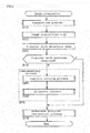
- step 11 (hereinafter, "step” is written as "S")).
- the preparation process (S11) includes an imaging process for imaging the first region M including the F-mark 55 and a process for reading, from the storage device 22, the first template 70 indicating the shape of the F-mark 55.
- the image acquisition unit 31 acquires the image data 60 obtained by imaging the first region M stored in the storage device 22 (S12).
- the detection unit 32 scans the image data 60 using the first template 70 to detect the position of the F-mark 55 (S13).
- the image processing device 30 determines whether or not the position of the F-mark 55 is detected by scanning with the detection unit 32 (S14). Specifically, when all the seek lines 71 of the first template 70 intersect the edge in the image data 60 at a predetermined position in the edge-processed image data 60, it is determined that the F-mark 55 matching the first template 70 has been detected (S14: Yes).
- the position recognition unit 35 then recognizes the reference position of the board 50 based on the detection result of the F-mark 55 by scanning with the detection unit 32 (S16).
- the image processing device 30 determines that the position of the F-mark 55 has not been detected (S14: No). In this way, when the position of the F-mark 55 is not detectable due to a factor such as a lack of a portion of the F-mark 55, the complementary process that acquires the position of the F-mark 55 is executed (S15).
- the complementary process (S15) includes a setting process (S20) of the second template 80 and an alignment process (S30) of the image data 60 with the second template 80.
- the template acquisition unit 33 In the template setting process (S20) of the complementary process (S15), the template acquisition unit 33 newly generates a second template 80 or acquires an existing second template 80, thereby setting the second template 80 to be used in the subsequent alignment process (S30) .
- the image processing device 30 then appropriately executes the recognition process for recognizing the reference position of the board 50 during execution of the mounting process by the component mounting machine 10.
- image processing for detecting the position of the F-mark 55 may be performed a plurality of times in the mounting process for the same board 50.
- some or all portions of the F-mark 55 shape may be covered by the electronic component mounted in the mounting process, and the position of the F-mark 55 may not be detected. Therefore, when the position of the F-mark 55 is detected by scanning using the first template 70, the image processing device 30 stores the image data in the storage device 22 as "first image data 60B", in which the F-mark 55 is successfully detected during the recognition process, on the assumption that the image data used in the recognition process will be used in a later recognition process.
- the template acquisition unit 33 first determines whether or not the first image data 60B is stored in the storage device 22 (S21). That is, for the board which is the target of the mounting process currently being executed by the component mounting machine 10, if the recognition process of the reference position using the first template 70 has already been executed and the position of the F-mark 55 has been successfully detected in a board 50, it is determined that the first image data 60B is stored in the storage device 22 (S21: Yes).
- the template acquisition unit 33 acquires the first image data 60B, which is the image data used in the previous recognition process in which the position of the F-mark 55 was detected (S22). Subsequently, the template acquisition unit 33 executes a generation process for generating a second template 80 by executing image processing on the first image data 60B (S23).
- the template acquisition unit 33 executes image processing to make the first image data 60B transparent so that other image data 60 displayed with the second template 80 superimposed can be viewed.
- the template acquisition unit 33 may execute image processing such as edge processing or binarization so that the shape of the distinctive portion 53 of the board 50 is noticeable.
- the template acquisition unit 33 divides the first image data 60B into a plurality of sections 61, as shown in FIG. 7 . Then, the template acquisition unit 33 removes sections 61R (hatched portion in FIG. 7 ) which satisfy a predetermined condition from the plurality of sections 61.
- the sections to be removed 61R include sections in which electronic components are mounted to obtain the first image data 60B from the time of imaging to the present, and sections in which the complexity of the image exceeds a predetermined threshold value.
- the sections 61 in which electronic components are mounted are removed because the template including the sections 61 is unsuitable for the alignment process by visual measurement due to variation in appearance of the board 50.
- the sections 61 in which the complexity of the image exceeds the threshold value are removal targets because the edges are gathered together in a complex manner rendering the template including the sections 61 unsuitable for the alignment process by visual measurement.
- the template acquisition unit 33 executes image processing for removing regions which include the F-mark 55 in the first image data 60B. Since the position of the F-mark 55 cannot be detected by scanning using the first template 70, the first template 70 may not be entirely visible in the image data 60 which indicates the current state of the board 50. Therefore, the template acquisition unit 33 removes the sections 61 that include the F-mark 55, which does not match with the current appearance of the second template 80, and is configured to generate a second template 80 which conforms better to the alignment process by the visual measurement.
- a second template 80 that shows a distinctive portion 53 of the board 50 is newly generated. Since the position of the F-mark 55 was detected in the first image data 60B, the defining point 82 of the second template 80 is defined by the result of the detection and the positional relationship of the defining point 72 of the first template 70. That is, the defining point 82 indicates the position of the F-mark 55 in the image data 60 when the second template 80 is aligned with the image data 60.
- the template acquisition unit 33 determines whether or not substitute image data that can substitute for the first image data 60B is stored in the storage device 22 (S24).
- Substitute image data is, for example, image data obtained by imaging in advance a board of the same type as the board 50 to be subjected to the mounting process. If substitute image data is stored (S24: Yes), the template acquisition unit 33 acquires the substitute image data (S25). The template acquisition unit 33 then performs image processing such as making the substitute image data transparent and generates a second template 80 (S23).
- the template acquisition unit 33 determines whether or not substitution by the existing second template (hereinafter, referred to as the "former second template") used in the other board 50 is possible (S26).
- the appearance of the board 50 differs depending on the mounting state of the electronic component and the printing state of the solder. Therefore, in the complementary process (S15) during execution of the mounting process, it is desirable to generate the second template 80 by using the first image data 60B obtained by imaging the target board 50.
- the template acquisition unit 33 determines whether or not the former second template can be substituted based on the type of the board 50 targeted for the image processing and the imaging region of the first image data which is the material of the former second template (S26).
- the template acquisition unit 33 acquires the former second template as the second template 80 in the current complementary process (S27).
- the template acquisition unit 33 acquires the first template 70 (S28).
- the display device 23 displays the second template 80 superimposed on the image data 60, as shown in FIG. 8 (S31).
- a cursor is arranged on each of four sides of the rectangular second template 80.
- the display device 23 also displays the degree of matching based on the relative position of the second template 80 with respect to the distinctive portion 53 of the board 50.
- the degree of matching between the distinctive portion 53 and the second template 80 is, for example, a value indicating how much the standard lines 81 of the second template 80 overlap with the edges in the image data 60.
- the display device 23 displays the degree of matching in numerical values as shown in the lower part of FIG. 8 .
- the display device 23 may display the degree of matching with a display color or line type of the standard line 81 of the second template 80.
- the input device 24 receives an operation for aligning the second template 80 with respect to the image data 60 (S32).
- the operator adjusts, for example, the state of overlap between the lands 51 and the standard lines 81 of the second template 80 in the image data 60 with reference to, for example, the numerical degree of matching.
- the position recognition unit 35 recognizes the reference position of the board 50 based on the content of the setting and the positional relationship with the reference position defined by the defining point 82 of the second template 80 (S16).
- the display device 23 displays the first template 70 superimposed on the image data 60, and the input device 24 receives an operation for aligning the first template 70 with the image data 60 (S32).
- the position recognition unit 35 recognizes the reference position of the board 50 based on the position of the defining point 72 of the aligned first template 70 (S16).
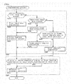
- the complementary process (S115) includes a setting process (S20) of the second template 80, a second detection process (S140) of performing re-detection using the second template 80, and a alignment process (S30).
- the second template 80 in the present embodiment is used for re-detection by the detection unit 32 as described above, image processing suitable for the detection process is executed. Specifically, in the generation process (S23) for generating the second template 80, the template acquisition unit 33 executes image processing for extracting an edge corresponding to the distinctive portion 53 of the board 50. Thus, the extracted edge is defined as the standard line 81 of the second template 80.
- the image processing device 30 After the template acquisition unit 33 executes the template setting process (S 20) in the complementary process (S115), the image processing device 30 first determines whether or not the second template 80 has been obtained (S141). When the former second template that can be newly generated or substituted is acquired as the second template 80 (S141: Yes), the detection unit 32 scans the image data 60 using the acquired second template 80 to detect the position of the distinctive portion 53 of the board 50. That is, the detection unit 32 performs detection using the second template 80 again.
- the image processing device 30 determines whether or not the position of the distinctive portion 53 of the board 50 is detected by the scanning of the detector 32 (S143). Specifically, when all the normal lines 81 of the second template 80 coincide with the edge of the image data 60 at a predetermined position in the edge-processed image data 60, it is determined that the distinctive portion 53 that matches with the second template 80 has been detected (S143: Yes). From this, the alignment process (S30) by the operator is omitted, and the complementary process (S115) is ended. Thereafter, the position recognition unit 35 recognizes the reference position of the board 50 based on the detection result for the distinctive portion 53 in the scanning by the detection unit 32 (S16).
- the image processing device 30 determines that the position of the distinctive portion 53 is not detected (S143: No).
- the position of the distinctive portion 53 corresponding to the position of the F-mark 55 cannot be detected even when the automatic re-detection process is executed, or when the second template 80 cannot be acquired in the template setting process (S20) (S141: No)
- the alignment process (S30) by the operator's manual operation is executed, and the complementary process (S115) is ended.
- the position recognition unit 35 recognizes the reference position of the board 50 (S16) based on the content of the setting in the alignment process.
- the image processing device 30 for a board includes an image acquisition unit 31 that acquires image data 60 obtained by capturing an image of a first region M that includes a fiduciary mark (F-mark 55) disposed on an upper surface of the board 50, a detection unit 32 that scans the image data 60 using a first template 70 that shows the shape of the fiduciary mark (F-mark 55) and detects the position of the fiduciary mark (F-mark 55) by scanning, and a template acquisition unit 33 that acquires a second template that shows a distinctive portion 53 of the board 50 disposed outside of the F-mark 55 in the first region M when the position of the F-mark 55 is not detected by the detection unit 32.
- an image acquisition unit 31 that acquires image data 60 obtained by capturing an image of a first region M that includes a fiduciary mark (F-mark 55) disposed on an upper surface of the board 50
- a detection unit 32 that scans the image data 60 using a first template 70 that shows the shape of the fiduciary mark (
- the image processing method for a board includes an image acquisition step (S12) of acquiring the image data 60 obtained by imaging the first region M that includes the fiduciary mark (F-mark 55) disposed on the upper surface of the board 50, a detection step (S13) of scanning the image data 60 using the first template 70 that shows the shape of the fiduciary mark (F-mark 55) and detecting the position of the fiduciary mark (F-mark 55) by scanning (S14 : No), and a template acquisition step (S20) of acquiring a second template that shows a distinctive portion 53 of the board 50 disposed outside of the fiducial mark (F-mark 55) in the first region M when the position of the fiducial mark (F-mark 55) is not detected (S14: No) by scanning in the detection step (S13).
- the reference position of the board 50 is recognized by using the second template 80 that shows the other distinctive portion 53 included in the same first region M.
- the complementary process (S15, S115) that uses the second template 80 can be executed, and the reference position can be recognized with higher accuracy than setting the reference position of the board 50 by manual manipulation of the operator (S16).
- the acquired image data 60 using the first template 70 can be redirected for use in the initial detection process (S13) .
- the processing efficiency in the image processing can be improved, and the time required for the complementary process (S15, S115) can be shortened.
- the image processing device 30 includes a display unit (display device 23) that displays the acquired second template 80 superimposed on the image data 60 and a setting receiving unit (input device 24) that receives the setting of the relative position of the second template 80 with respect to the image data 60.
- the position recognition unit 35 recognizes the reference position of the board 50 based on the content of the setting (S30) and the positional relationship with the reference position defined in the second template 80 (S16).
- the reference position of the board 50 can be recognized by reflecting the content of the setting input by the operator.
- the operator performs an operation to align the template with the F-mark 55.
- the F-mark 55 is not detectable by the image processing device 30 due to a factor such as a lack of a portion of the F-mark 55, and it is not easy for the operator to accurately perform alignment by visual measurement.
- the second template 80 positioned around the F-mark 55 is displayed on the image data 60 so as to be superimposed on the image data 60. Therefore, even when the setting is performed by visual measurement of the operator, the relative position of the second template 80 with respect to the image data 60 can be more accurately set than aligning the F-mark 55 with the second template 80. As a result, the reference position can be recognized with high accuracy.
- the display unit i.e., the display device 23
- the display unit also displays the degree of matching based on the relative position of the second template 80 with respect to the distinctive portion 53 of the board 50.
- the operator can set the relative position of the second template 80 with respect to the image data 60 with reference to the displayed degree of matching (S32).
- the relative position can be set with higher accuracy. Therefore, the reference position of the board 50 can be recognized with high accuracy.
- the detection unit 32 scans the image data 60 using the acquired second template 80 to detect the position of the distinctive portion 53 (S142).
- the position recognition unit 35 recognizes the reference position of the board 50 based on the detection result by the detection unit 32 and the positional relationship with the reference position defined in the second template 80 (S16) .
- the detection unit 32 (S142) re-scans the image data 60 using the second template 80 that can be used in the same first region M.
- the operator omits manual operations such as aligning the template with respect to the image data 60 (S143: Yes), and the reference position of the board 50 is automatically recognized (S16). Therefore, the processing efficiency in the image processing can be improved, and the time required for the complementary processing (S115) can be shortened.
- the image processing device 30 is applied to the component mounting machine 10 that mounts a plurality of electronic components on the board 50 and performs a recognition process for recognizing a reference position during multiple executions of the mounting process by the component mounting machine 10.
- the template acquisition unit 33 acquires the first image data 60, which is the image data 60 used in the previous recognition process in which the position of the fiducial mark (F-mark 55) is detected (S22), and executes image processing for making the first image data 60 transparent or image processing for extracting the edge corresponding to the distinctive portion 53 to generate the second template 80 (S23).
- the second template 80 is generated from the first image data 60 that was used in the past rather than the current detection process and in which the fiduciary mark (F-mark 55) was successfully detected.
- the second template 80 can be generated which is suitable for detecting the distinctive portion 53 by reflecting a state unique to the board 50 (i.e., the state of the wiring pattern, the state of the solder printing, and the state of the mounted electronic component).
- the template acquisition unit 33 executes image processing for removing a region including the fiducial mark (F-mark 55) in the first image data 60 (see FIG. 7 ).
- the region including the fiducial mark (F-mark 55) is removed from the second template 80.
- the fiducial mark (F-mark 55) is not detectable by the image processing device 30 due to a factor such as a lack of a portion of the F-mark 55, for example. Therefore, if the second template 80 includes a region including the fiducial mark (F-mark 55), there is a possibility that processes such as subsequent scanning and aligning may be affected. Therefore, with the above-described configuration, it is possible to remove inconsistent regions in advance and adapt the second template 80 with the complementary process (S15, S115).
- the template acquisition unit 33 divides the first image data 60 into a plurality of sections 61, and executes image processing for removing the section 61R on which the electronic component is mounted from the plurality of sections 61 or the section 61R in which the complexity of the image exceeds a predetermined threshold value (see FIG. 7 ) .
- the section 61R is specifically removed from the second template 80.
- the first image data 60 that has been used in the previous detection process and has successfully detected the F-mark 55 includes a region in which a state unique to the board 50 (e.g., the state of the mounted electronic component) varies depending on the subsequent execution of the mounting process and the first image data 60 cannot be used as the distinctive portion 53 in the complementary process (S15, S115).
- the second template 80 can be adapted by the complementary process (S15, S115) by removing sections in which the state unique to the board varies and the sections in which the complexity of the image exceeds a certain level.
- the fiducial mark disposed on the upper surface of the board 50 is the F-mark 55.
- the image processing device 30 may adopt a distinctive portion of the board 50, such as a portion of the wiring pattern of the board 50, as a fiducial mark. This is applied, for example, when the F-mark 55 is omitted to increase the density of the board 50, or when the positional relationship between the F-mark 55 and the wiring pattern is not constant due to the structure of the board 50.
- a portion of the plurality of distinctive portions included in the first region M is used as a fiducial mark.
- another portion of the plurality of distinctive portions included in the first area M is detected in the complementary process (S 15, S115).
- the image processing device 30 is applied to the control device 20 of the component mounting machine 10.
- the image processing device and the image processing method for a board can be applied to other production facilities such as a screen printer, a mounting inspector, or the host computer 2. In such a configuration, the same effects as those of the first and second embodiments are obtained.
Landscapes
- Engineering & Computer Science (AREA)
- Physics & Mathematics (AREA)
- General Physics & Mathematics (AREA)
- Theoretical Computer Science (AREA)
- Computer Vision & Pattern Recognition (AREA)
- Manufacturing & Machinery (AREA)
- Microelectronics & Electronic Packaging (AREA)
- Supply And Installment Of Electrical Components (AREA)
- Image Analysis (AREA)
- Image Processing (AREA)
Claims (5)
- Bildverarbeitungsvorrichtung (30) für eine Leiterplatte (50), umfassend:eine Bilderfassungseinheit (31), die dazu konfiguriert ist, Bilddaten (60) durch Aufnehmen eines Bildes eines ersten Bereichs (M) einschließlich einer Bezugsmarkierung (55) zu erfassen, die auf einer Oberseite der Leiterplatte (50) angeordnet ist;eine Ermittlungseinheit (32), die dazu konfiguriert ist, die Bilddaten (60) unter Verwendung einer ersten Schablone (70) abzutasten, welche eine Form der Bezugsmarkierung (55) anzeigt, um eine Position der Bezugsmarkierung (55) zu ermitteln, wobei die Positionsbeziehung der ersten Schablone (70) zu einer Referenzposition der Leiterplatte (50) bekannt ist;eine Schablonenerfassungseinheit (33), die dazu konfiguriert ist, eine zweite Schablone (80) neu zu erzeugen oder eine vorhandene zweite Schablone (80) zu erfassen, die bereits in einer anderen Leiterplatte erzeugt wurde, wobei die zweite Schablone (80) einen bestimmten Abschnitt (53) der Leiterplatte (50) anzeigt, der sich außerhalb der Bezugsmarkierung (55) in dem ersten Bereich (M) befindet, wenn die Position der Bezugsmarkierung (55) durch Abtasten mit der Ermittlungseinheit (32) nicht ermittelt wird;eine Positionserkennungseinheit (35), die dazu konfiguriert ist, die Referenzposition der Leiterplatte (50) basierend auf der Ermittlung der Position der Bezugsmarkierung (55) zu erkennen, und dazu konfiguriert ist, die Referenzposition der Leiterplatte (50) unter Verwendung der zweiten Schablone (80) zu erkennen, wenn die Position der Bezugsmarkierung (55) durch Abtasten mit der Ermittlungseinheit (32) nicht ermittelt wird,wobeieine Anzeigeeinheit (23) dazu konfiguriert ist, die erfasste zweite Schablone (80) überlagert auf den Bilddaten (60) anzuzeigen, undeine Einstellungsempfangseinheit (24) dazu konfiguriert ist, eine Einstellung einer relativen Position der zweiten Schablone (80) bezüglich der Bilddaten (60) zu empfangen,wobeidie Positionserkennungseinheit (35) die Referenzposition der Leiterplatte (50) basierend auf Inhalt der Einstellung und einer bekannten Positionsbeziehung der zweiten Schablone (80) zu der Referenzposition der Leiterplatte (50) erkennt;wobei die Bildverarbeitungsvorrichtung (30) des Weiteren dazu konfiguriert ist, auf eine Komponentenmontagemaschine (10) angewendet zu werden, die eine Vielzahl von elektronischen Komponenten auf der Leiterplatte (50) montiert, und den Erkennungsprozess zum Erkennen der Referenzposition eine Vielzahl von Malen während der Ausführung des Montageprozesses durch die Komponentenmontagemaschine (10) auszuführen,wobei die Schablonenerfassungseinheit (33) des Weiteren dazu konfiguriert ist, erste Bilddaten (60B) zu erfassen, bei welchen es sich um die Bilddaten handelt, die in dem vorhergehenden Erkennungsprozess verwendet wurden, in welchem eine Position der Bezugsmarkierung (55) ermittelt wurde, und die Bildverarbeitung auszuführen, um die ersten Bilddaten (60B) transparent zu machen, so dass weitere Bilddaten, die mit der zweiten Schablone angezeigt werden, betrachtet werden können, oder die Bildverarbeitung zum Extrahieren einer Kante entsprechend dem bestimmten Abschnitt (53) auszuführen, um die zweite Schablone (80) zu erzeugen;wobeidie Schablonenerfassungseinheit (33) des Weiteren dazu konfiguriert ist, die Bildverarbeitung zum Entfernen eines Bereiches einschließlich der Bezugsmarkierung (55) in den ersten Bilddaten (60B) in dem Erzeugungsprozess zum Erzeugen der zweiten Schablone (80) auszuführen.
- Bildverarbeitungsvorrichtung (30) für eine Leiterplatte (50) nach Anspruch 1, wobei
die Anzeigeeinheit (23) dazu konfiguriert ist, einen Übereinstimmungsgrad basierend auf der relativen Position der zweiten Schablone (80) bezüglich dem bestimmten Abschnitt (53) der Leiterplatte (50) zusammen anzuzeigen, wenn die zweite Schablone (80) in überlappender Weise auf den Bilddaten (60) angezeigt wird. - Bildverarbeitungsvorrichtung (30) für eine Leiterplatte (50) nach Anspruch 1 oder 2, wobei
die Ermittlungseinheit (32) dazu konfiguriert ist, die Bilddaten (60) unter Verwendung der erfassten zweiten Schablone (80) abzutasten, um eine Position des bestimmten Abschnitts (53) zu ermitteln, und die Positionserkennungseinheit (35) dazu konfiguriert ist, die Referenzposition der Leiterplatte (50) basierend auf einem Ermittlungsergebnis durch die Ermittlungseinheit (32) und einer bekannten Positionsbeziehung der zweiten Schablone (80) zu der Referenzposition der Leiterplatte (50) zu erkennen. - Bildverarbeitungsvorrichtung (30) für eine Leiterplatte (50) nach Anspruch 1, wobei
die Schablonenerfassungseinheit (33) dazu konfiguriert ist, die ersten Bilddaten (60B) in eine Vielzahl von Abschnitten (61) aufzuteilen und dazu konfiguriert ist, die Bildverarbeitung zum Entfernen eines Abschnitts (61), in dem eine elektronische Komponente montiert ist, oder eines Abschnitts (61), in dem die Anzahl von Umrisslinien des Bildes einen vorgegebenen Schwellenwert überschreitet, aus der Vielzahl von Abschnitten (61) in dem Erzeugungsprozess zum Erzeugen der zweiten Schablone (80) auszuführen. - Bildverarbeitungsverfahren für eine Leiterplatte (50), umfassend:Erfassen von Bilddaten (60), die durch Aufnehmen eines Bildes eines ersten Bereiches (M) erhalten werden, der eine Bezugsmarkierung enthält, die auf einer Oberseite der Leiterplatte (50) angeordnet ist;Abtasten der Bilddaten (60) unter Verwendung einer ersten Schablone (70), welche eine Form der Bezugsmarkierung zeigt, um eine Position der Bezugsmarkierung (55) zu ermitteln, wobei die Positionsbeziehung der ersten Schablone (70) zu der Referenzposition der Leiterplatte (50) bekannt ist;Erzeugen einer neuen zweiten Schablone oder Erfassen einer vorhandenen zweiten Schablone (80), die bereits in einer anderen Leiterplatte erzeugt wurde, wobei die zweite Schablone (80) einen bestimmten Abschnitt (53) der Leiterplatte (50) anzeigt, der sich außerhalb der Bezugsmarkierung in dem ersten Bereich (M) befindet, falls die Position der Bezugsmarkierung durch Abtasten nicht ermittelt wird; undErkennen der Referenzposition der Leiterplatte (50) basierend auf dem Ermittlungsergebnis der Position der Bezugsmarkierung (55) und Erkennen der Referenzposition der Leiterplatte (50) unter Verwendung der zweiten Schablone (80), wenn die Position der Bezugsmarkierung (55) durch Abtasten nicht ermittelt wird, undAnzeigen der erfassten zweiten Schablone (80) überlagert auf den Bilddaten (60), undEmpfangen einer Einstellung einer relativen Position der zweiten Schablone (80) bezüglich der Bilddaten (60), undErkennen der Referenzposition der Leiterplatte (50) basierend auf Inhalt der Einstellung und einer bekannten Positionsbeziehung der zweiten Schablone (80) zu der Referenzposition der Leiterplatte (50), wobeidas Bildverarbeitungsverfahren für eine Leiterplatte (50) des Weiteren beinhaltet:Montieren einer Vielzahl von elektronischen Komponenten auf der Leiterplatte (50), Erkennen der Referenzposition eine Vielzahl von Malen während der Ausführung des Montageprozesses durch die Komponentenmontagemaschine (10),Erfassen von ersten Bilddaten (60B), bei welchen es sich um die Bilddaten handelt, die in dem vorhergehenden Erkennungsprozess verwendet wurden, in welchem eine Position der Bezugsmarkierung (55) ermittelt wurde, und die Bildverarbeitung auszuführen, um die ersten Bilddaten (60B) transparent zu machen, so dass weitere Bilddaten, die mit der zweiten Schablone angezeigt werden, betrachtet werden können, oder die Bildverarbeitung zum Extrahieren einer Kante entsprechend dem bestimmten Abschnitt (53), um die zweite Schablone (80) zu erzeugen;wobei die Bildverarbeitung des Weiteren umfasst:
Ausführen der Bildverarbeitung zum Entfernen eines Bereiches einschließlich der Bezugsmarkierung (55) in den ersten Bilddaten (60B) in dem Erzeugungsprozess zum Erzeugen der zweiten Schablone (80).
Applications Claiming Priority (1)
| Application Number | Priority Date | Filing Date | Title |
|---|---|---|---|
| PCT/JP2015/084303 WO2017098561A1 (ja) | 2015-12-07 | 2015-12-07 | 基板用の画像処理装置および画像処理方法 |
Publications (3)
| Publication Number | Publication Date |
|---|---|
| EP3389007A1 EP3389007A1 (de) | 2018-10-17 |
| EP3389007A4 EP3389007A4 (de) | 2018-11-14 |
| EP3389007B1 true EP3389007B1 (de) | 2020-06-10 |
Family
ID=59012869
Family Applications (1)
| Application Number | Title | Priority Date | Filing Date |
|---|---|---|---|
| EP15910178.1A Active EP3389007B1 (de) | 2015-12-07 | 2015-12-07 | Substratbildverarbeitungsvorrichtung und substratbildverarbeitungsverfahren |
Country Status (3)
| Country | Link |
|---|---|
| EP (1) | EP3389007B1 (de) |
| JP (1) | JP6734868B2 (de) |
| WO (1) | WO2017098561A1 (de) |
Families Citing this family (5)
| Publication number | Priority date | Publication date | Assignee | Title |
|---|---|---|---|---|
| EP3644702B1 (de) * | 2017-06-21 | 2022-07-13 | Fuji Corporation | Vorrichtung zur durchführung von arbeit auf einem substrat |
| JP7090219B2 (ja) * | 2017-09-13 | 2022-06-24 | パナソニックIpマネジメント株式会社 | 位置特定方法および位置特定装置 |
| CN108717697B (zh) * | 2018-05-18 | 2021-04-13 | 广州视源电子科技股份有限公司 | 电路板检测方法、装置、计算机设备和存储介质 |
| JP7601215B2 (ja) * | 2021-04-23 | 2024-12-17 | 日本電気株式会社 | 制御装置、制御方法及びプログラム |
| CN115511829A (zh) * | 2022-09-27 | 2022-12-23 | 昆山鸿富洋科技有限公司 | 一种ng物料图形化比对核验方法 |
Family Cites Families (5)
| Publication number | Priority date | Publication date | Assignee | Title |
|---|---|---|---|---|
| JP2002157582A (ja) * | 2000-11-21 | 2002-05-31 | Matsushita Electric Ind Co Ltd | 半導体ウエハ上のic傾き補正方法、及びic傾き補正装置 |
| JP2005116561A (ja) * | 2003-10-02 | 2005-04-28 | Nikon Corp | テンプレート作成方法及び装置、位置検出方法及び装置、並びに露光方法及び装置 |
| JP4337757B2 (ja) * | 2004-09-29 | 2009-09-30 | カシオ計算機株式会社 | 撮影装置、撮影システム、及びプログラム |
| CN101996398B (zh) * | 2009-08-12 | 2012-07-04 | 睿励科学仪器(上海)有限公司 | 用于晶圆对准的图像匹配方法及设备 |
| JP6646916B2 (ja) * | 2015-11-11 | 2020-02-14 | 株式会社Fuji | 基板用の画像処理装置および画像処理方法 |
-
2015
- 2015-12-07 WO PCT/JP2015/084303 patent/WO2017098561A1/ja not_active Ceased
- 2015-12-07 EP EP15910178.1A patent/EP3389007B1/de active Active
- 2015-12-07 JP JP2017554682A patent/JP6734868B2/ja active Active
Non-Patent Citations (1)
| Title |
|---|
| None * |
Also Published As
| Publication number | Publication date |
|---|---|
| JPWO2017098561A1 (ja) | 2018-09-27 |
| JP6734868B2 (ja) | 2020-08-05 |
| WO2017098561A1 (ja) | 2017-06-15 |
| EP3389007A4 (de) | 2018-11-14 |
| EP3389007A1 (de) | 2018-10-17 |
Similar Documents
| Publication | Publication Date | Title |
|---|---|---|
| EP3389007B1 (de) | Substratbildverarbeitungsvorrichtung und substratbildverarbeitungsverfahren | |
| JP5798371B2 (ja) | 基準マークモデルテンプレート作成方法 | |
| US20230403835A1 (en) | Support pin arrangement determination assisting apparatus | |
| US20120189188A1 (en) | Component mounting system and mounting state inspection method in the component mounting system | |
| US10070570B2 (en) | Mounting device, image processing method, and imaging unit | |
| EP3376844B1 (de) | Bildverarbeitungsvorrichtung und bildverarbeitungsverfahren für grundplatte | |
| JP6571116B2 (ja) | 検査支援装置 | |
| EP3410834B1 (de) | Vorrichtung zur montage einer elektronischen komponente und fertigungslinie | |
| EP2975921A1 (de) | Komponentenerkennungssystem für eine komponentenmontagemaschine | |
| JP7094282B2 (ja) | 対基板作業装置 | |
| JP6608543B2 (ja) | 画像処理システム及び画像処理方法 | |
| JP6904978B2 (ja) | 部品装着機 | |
| JP5443894B2 (ja) | 電子部品実装装置及びその吸着位置補正方法 | |
| JP2017224779A (ja) | 実装関連処理装置 | |
| JP6833871B2 (ja) | 画像処理用部品データ作成方法及び画像処理用部品データ作成システム | |
| JP2017072924A (ja) | 基板用の画像処理装置 | |
| WO2020183735A1 (ja) | 良否判定装置および良否判定方法 | |
| US20260024187A1 (en) | Image output device and image output system | |
| JP2024112222A (ja) | 検査システム | |
| CN120051797A (zh) | 线设定装置及具备该线设定装置的元件安装机 | |
| JP4882849B2 (ja) | 基板外観検査における検査ウィンドウの設定用データの作成方法および設定用データ作成システム | |
| CN110678060A (zh) | 图像处理装置、安装装置、图像处理方法、存储介质 | |
| KR20150081159A (ko) | 인쇄정렬장치 및 인쇄방법 |
Legal Events
| Date | Code | Title | Description |
|---|---|---|---|
| STAA | Information on the status of an ep patent application or granted ep patent |
Free format text: STATUS: THE INTERNATIONAL PUBLICATION HAS BEEN MADE |
|
| PUAI | Public reference made under article 153(3) epc to a published international application that has entered the european phase |
Free format text: ORIGINAL CODE: 0009012 |
|
| STAA | Information on the status of an ep patent application or granted ep patent |
Free format text: STATUS: REQUEST FOR EXAMINATION WAS MADE |
|
| 17P | Request for examination filed |
Effective date: 20180606 |
|
| AK | Designated contracting states |
Kind code of ref document: A1 Designated state(s): AL AT BE BG CH CY CZ DE DK EE ES FI FR GB GR HR HU IE IS IT LI LT LU LV MC MK MT NL NO PL PT RO RS SE SI SK SM TR |
|
| AX | Request for extension of the european patent |
Extension state: BA ME |
|
| A4 | Supplementary search report drawn up and despatched |
Effective date: 20181016 |
|
| RIC1 | Information provided on ipc code assigned before grant |
Ipc: G06T 1/00 20060101ALI20181008BHEP Ipc: G06T 7/00 20170101AFI20181008BHEP Ipc: G06T 7/73 20170101ALI20181008BHEP Ipc: H05K 13/04 20060101ALI20181008BHEP |
|
| RIN1 | Information on inventor provided before grant (corrected) |
Inventor name: TERAOKA SEIICHI |
|
| DAV | Request for validation of the european patent (deleted) | ||
| DAX | Request for extension of the european patent (deleted) | ||
| STAA | Information on the status of an ep patent application or granted ep patent |
Free format text: STATUS: EXAMINATION IS IN PROGRESS |
|
| 17Q | First examination report despatched |
Effective date: 20190725 |
|
| GRAP | Despatch of communication of intention to grant a patent |
Free format text: ORIGINAL CODE: EPIDOSNIGR1 |
|
| STAA | Information on the status of an ep patent application or granted ep patent |
Free format text: STATUS: GRANT OF PATENT IS INTENDED |
|
| INTG | Intention to grant announced |
Effective date: 20200225 |
|
| GRAS | Grant fee paid |
Free format text: ORIGINAL CODE: EPIDOSNIGR3 |
|
| GRAA | (expected) grant |
Free format text: ORIGINAL CODE: 0009210 |
|
| STAA | Information on the status of an ep patent application or granted ep patent |
Free format text: STATUS: THE PATENT HAS BEEN GRANTED |
|
| AK | Designated contracting states |
Kind code of ref document: B1 Designated state(s): AL AT BE BG CH CY CZ DE DK EE ES FI FR GB GR HR HU IE IS IT LI LT LU LV MC MK MT NL NO PL PT RO RS SE SI SK SM TR |
|
| REG | Reference to a national code |
Ref country code: GB Ref legal event code: FG4D |
|
| REG | Reference to a national code |
Ref country code: AT Ref legal event code: REF Ref document number: 1279778 Country of ref document: AT Kind code of ref document: T Effective date: 20200615 Ref country code: CH Ref legal event code: EP |
|
| REG | Reference to a national code |
Ref country code: DE Ref legal event code: R096 Ref document number: 602015054221 Country of ref document: DE |
|
| REG | Reference to a national code |
Ref country code: IE Ref legal event code: FG4D |
|
| REG | Reference to a national code |
Ref country code: LT Ref legal event code: MG4D |
|
| PG25 | Lapsed in a contracting state [announced via postgrant information from national office to epo] |
Ref country code: SE Free format text: LAPSE BECAUSE OF FAILURE TO SUBMIT A TRANSLATION OF THE DESCRIPTION OR TO PAY THE FEE WITHIN THE PRESCRIBED TIME-LIMIT Effective date: 20200610 Ref country code: GR Free format text: LAPSE BECAUSE OF FAILURE TO SUBMIT A TRANSLATION OF THE DESCRIPTION OR TO PAY THE FEE WITHIN THE PRESCRIBED TIME-LIMIT Effective date: 20200911 Ref country code: LT Free format text: LAPSE BECAUSE OF FAILURE TO SUBMIT A TRANSLATION OF THE DESCRIPTION OR TO PAY THE FEE WITHIN THE PRESCRIBED TIME-LIMIT Effective date: 20200610 Ref country code: FI Free format text: LAPSE BECAUSE OF FAILURE TO SUBMIT A TRANSLATION OF THE DESCRIPTION OR TO PAY THE FEE WITHIN THE PRESCRIBED TIME-LIMIT Effective date: 20200610 Ref country code: NO Free format text: LAPSE BECAUSE OF FAILURE TO SUBMIT A TRANSLATION OF THE DESCRIPTION OR TO PAY THE FEE WITHIN THE PRESCRIBED TIME-LIMIT Effective date: 20200910 |
|
| REG | Reference to a national code |
Ref country code: NL Ref legal event code: MP Effective date: 20200610 |
|
| PG25 | Lapsed in a contracting state [announced via postgrant information from national office to epo] |
Ref country code: RS Free format text: LAPSE BECAUSE OF FAILURE TO SUBMIT A TRANSLATION OF THE DESCRIPTION OR TO PAY THE FEE WITHIN THE PRESCRIBED TIME-LIMIT Effective date: 20200610 Ref country code: HR Free format text: LAPSE BECAUSE OF FAILURE TO SUBMIT A TRANSLATION OF THE DESCRIPTION OR TO PAY THE FEE WITHIN THE PRESCRIBED TIME-LIMIT Effective date: 20200610 Ref country code: LV Free format text: LAPSE BECAUSE OF FAILURE TO SUBMIT A TRANSLATION OF THE DESCRIPTION OR TO PAY THE FEE WITHIN THE PRESCRIBED TIME-LIMIT Effective date: 20200610 Ref country code: BG Free format text: LAPSE BECAUSE OF FAILURE TO SUBMIT A TRANSLATION OF THE DESCRIPTION OR TO PAY THE FEE WITHIN THE PRESCRIBED TIME-LIMIT Effective date: 20200910 |
|
| REG | Reference to a national code |
Ref country code: AT Ref legal event code: MK05 Ref document number: 1279778 Country of ref document: AT Kind code of ref document: T Effective date: 20200610 |
|
| PG25 | Lapsed in a contracting state [announced via postgrant information from national office to epo] |
Ref country code: AL Free format text: LAPSE BECAUSE OF FAILURE TO SUBMIT A TRANSLATION OF THE DESCRIPTION OR TO PAY THE FEE WITHIN THE PRESCRIBED TIME-LIMIT Effective date: 20200610 Ref country code: NL Free format text: LAPSE BECAUSE OF FAILURE TO SUBMIT A TRANSLATION OF THE DESCRIPTION OR TO PAY THE FEE WITHIN THE PRESCRIBED TIME-LIMIT Effective date: 20200610 |
|
| PG25 | Lapsed in a contracting state [announced via postgrant information from national office to epo] |
Ref country code: AT Free format text: LAPSE BECAUSE OF FAILURE TO SUBMIT A TRANSLATION OF THE DESCRIPTION OR TO PAY THE FEE WITHIN THE PRESCRIBED TIME-LIMIT Effective date: 20200610 Ref country code: SM Free format text: LAPSE BECAUSE OF FAILURE TO SUBMIT A TRANSLATION OF THE DESCRIPTION OR TO PAY THE FEE WITHIN THE PRESCRIBED TIME-LIMIT Effective date: 20200610 Ref country code: EE Free format text: LAPSE BECAUSE OF FAILURE TO SUBMIT A TRANSLATION OF THE DESCRIPTION OR TO PAY THE FEE WITHIN THE PRESCRIBED TIME-LIMIT Effective date: 20200610 Ref country code: CZ Free format text: LAPSE BECAUSE OF FAILURE TO SUBMIT A TRANSLATION OF THE DESCRIPTION OR TO PAY THE FEE WITHIN THE PRESCRIBED TIME-LIMIT Effective date: 20200610 Ref country code: IT Free format text: LAPSE BECAUSE OF FAILURE TO SUBMIT A TRANSLATION OF THE DESCRIPTION OR TO PAY THE FEE WITHIN THE PRESCRIBED TIME-LIMIT Effective date: 20200610 Ref country code: RO Free format text: LAPSE BECAUSE OF FAILURE TO SUBMIT A TRANSLATION OF THE DESCRIPTION OR TO PAY THE FEE WITHIN THE PRESCRIBED TIME-LIMIT Effective date: 20200610 Ref country code: PT Free format text: LAPSE BECAUSE OF FAILURE TO SUBMIT A TRANSLATION OF THE DESCRIPTION OR TO PAY THE FEE WITHIN THE PRESCRIBED TIME-LIMIT Effective date: 20201012 Ref country code: ES Free format text: LAPSE BECAUSE OF FAILURE TO SUBMIT A TRANSLATION OF THE DESCRIPTION OR TO PAY THE FEE WITHIN THE PRESCRIBED TIME-LIMIT Effective date: 20200610 |
|
| PG25 | Lapsed in a contracting state [announced via postgrant information from national office to epo] |
Ref country code: IS Free format text: LAPSE BECAUSE OF FAILURE TO SUBMIT A TRANSLATION OF THE DESCRIPTION OR TO PAY THE FEE WITHIN THE PRESCRIBED TIME-LIMIT Effective date: 20201010 Ref country code: SK Free format text: LAPSE BECAUSE OF FAILURE TO SUBMIT A TRANSLATION OF THE DESCRIPTION OR TO PAY THE FEE WITHIN THE PRESCRIBED TIME-LIMIT Effective date: 20200610 Ref country code: PL Free format text: LAPSE BECAUSE OF FAILURE TO SUBMIT A TRANSLATION OF THE DESCRIPTION OR TO PAY THE FEE WITHIN THE PRESCRIBED TIME-LIMIT Effective date: 20200610 |
|
| REG | Reference to a national code |
Ref country code: DE Ref legal event code: R097 Ref document number: 602015054221 Country of ref document: DE |
|
| PLBE | No opposition filed within time limit |
Free format text: ORIGINAL CODE: 0009261 |
|
| STAA | Information on the status of an ep patent application or granted ep patent |
Free format text: STATUS: NO OPPOSITION FILED WITHIN TIME LIMIT |
|
| PG25 | Lapsed in a contracting state [announced via postgrant information from national office to epo] |
Ref country code: DK Free format text: LAPSE BECAUSE OF FAILURE TO SUBMIT A TRANSLATION OF THE DESCRIPTION OR TO PAY THE FEE WITHIN THE PRESCRIBED TIME-LIMIT Effective date: 20200610 |
|
| 26N | No opposition filed |
Effective date: 20210311 |
|
| PG25 | Lapsed in a contracting state [announced via postgrant information from national office to epo] |
Ref country code: SI Free format text: LAPSE BECAUSE OF FAILURE TO SUBMIT A TRANSLATION OF THE DESCRIPTION OR TO PAY THE FEE WITHIN THE PRESCRIBED TIME-LIMIT Effective date: 20200610 |
|
| REG | Reference to a national code |
Ref country code: CH Ref legal event code: PL |
|
| GBPC | Gb: european patent ceased through non-payment of renewal fee |
Effective date: 20201207 |
|
| PG25 | Lapsed in a contracting state [announced via postgrant information from national office to epo] |
Ref country code: MC Free format text: LAPSE BECAUSE OF FAILURE TO SUBMIT A TRANSLATION OF THE DESCRIPTION OR TO PAY THE FEE WITHIN THE PRESCRIBED TIME-LIMIT Effective date: 20200610 |
|
| REG | Reference to a national code |
Ref country code: BE Ref legal event code: MM Effective date: 20201231 |
|
| PG25 | Lapsed in a contracting state [announced via postgrant information from national office to epo] |
Ref country code: FR Free format text: LAPSE BECAUSE OF NON-PAYMENT OF DUE FEES Effective date: 20201231 Ref country code: LU Free format text: LAPSE BECAUSE OF NON-PAYMENT OF DUE FEES Effective date: 20201207 Ref country code: IE Free format text: LAPSE BECAUSE OF NON-PAYMENT OF DUE FEES Effective date: 20201207 |
|
| PG25 | Lapsed in a contracting state [announced via postgrant information from national office to epo] |
Ref country code: CH Free format text: LAPSE BECAUSE OF NON-PAYMENT OF DUE FEES Effective date: 20201231 Ref country code: GB Free format text: LAPSE BECAUSE OF NON-PAYMENT OF DUE FEES Effective date: 20201207 Ref country code: LI Free format text: LAPSE BECAUSE OF NON-PAYMENT OF DUE FEES Effective date: 20201231 |
|
| PG25 | Lapsed in a contracting state [announced via postgrant information from national office to epo] |
Ref country code: IS Free format text: LAPSE BECAUSE OF FAILURE TO SUBMIT A TRANSLATION OF THE DESCRIPTION OR TO PAY THE FEE WITHIN THE PRESCRIBED TIME-LIMIT Effective date: 20201010 Ref country code: TR Free format text: LAPSE BECAUSE OF FAILURE TO SUBMIT A TRANSLATION OF THE DESCRIPTION OR TO PAY THE FEE WITHIN THE PRESCRIBED TIME-LIMIT Effective date: 20200610 Ref country code: MT Free format text: LAPSE BECAUSE OF FAILURE TO SUBMIT A TRANSLATION OF THE DESCRIPTION OR TO PAY THE FEE WITHIN THE PRESCRIBED TIME-LIMIT Effective date: 20200610 Ref country code: CY Free format text: LAPSE BECAUSE OF FAILURE TO SUBMIT A TRANSLATION OF THE DESCRIPTION OR TO PAY THE FEE WITHIN THE PRESCRIBED TIME-LIMIT Effective date: 20200610 |
|
| PG25 | Lapsed in a contracting state [announced via postgrant information from national office to epo] |
Ref country code: MK Free format text: LAPSE BECAUSE OF FAILURE TO SUBMIT A TRANSLATION OF THE DESCRIPTION OR TO PAY THE FEE WITHIN THE PRESCRIBED TIME-LIMIT Effective date: 20200610 |
|
| PG25 | Lapsed in a contracting state [announced via postgrant information from national office to epo] |
Ref country code: BE Free format text: LAPSE BECAUSE OF NON-PAYMENT OF DUE FEES Effective date: 20201231 |
|
| P01 | Opt-out of the competence of the unified patent court (upc) registered |
Effective date: 20230328 |
|
| PGFP | Annual fee paid to national office [announced via postgrant information from national office to epo] |
Ref country code: DE Payment date: 20251028 Year of fee payment: 11 |