EP3384687B1 - Trans-impedance amplifier for ultrasound device and related apparatus and methods - Google Patents
Trans-impedance amplifier for ultrasound device and related apparatus and methods Download PDFInfo
- Publication number
- EP3384687B1 EP3384687B1 EP16871463.2A EP16871463A EP3384687B1 EP 3384687 B1 EP3384687 B1 EP 3384687B1 EP 16871463 A EP16871463 A EP 16871463A EP 3384687 B1 EP3384687 B1 EP 3384687B1
- Authority
- EP
- European Patent Office
- Prior art keywords
- stage
- current
- variable current
- variable
- amplifier
- Prior art date
- Legal status (The legal status is an assumption and is not a legal conclusion. Google has not performed a legal analysis and makes no representation as to the accuracy of the status listed.)
- Active
Links
Images


Classifications
-
- H—ELECTRICITY
- H03—ELECTRONIC CIRCUITRY
- H03F—AMPLIFIERS
- H03F3/00—Amplifiers with only discharge tubes or only semiconductor devices as amplifying elements
- H03F3/04—Amplifiers with only discharge tubes or only semiconductor devices as amplifying elements with semiconductor devices only
- H03F3/16—Amplifiers with only discharge tubes or only semiconductor devices as amplifying elements with semiconductor devices only with field-effect devices
-
- H—ELECTRICITY
- H03—ELECTRONIC CIRCUITRY
- H03F—AMPLIFIERS
- H03F1/00—Details of amplifiers with only discharge tubes, only semiconductor devices or only unspecified devices as amplifying elements
- H03F1/08—Modifications of amplifiers to reduce detrimental influences of internal impedances of amplifying elements
- H03F1/083—Modifications of amplifiers to reduce detrimental influences of internal impedances of amplifying elements in transistor amplifiers
- H03F1/086—Modifications of amplifiers to reduce detrimental influences of internal impedances of amplifying elements in transistor amplifiers with FET's
-
- A—HUMAN NECESSITIES
- A61—MEDICAL OR VETERINARY SCIENCE; HYGIENE
- A61B—DIAGNOSIS; SURGERY; IDENTIFICATION
- A61B5/00—Measuring for diagnostic purposes; Identification of persons
- A61B5/68—Arrangements of detecting, measuring or recording means, e.g. sensors, in relation to patient
- A61B5/6801—Arrangements of detecting, measuring or recording means, e.g. sensors, in relation to patient specially adapted to be attached to or worn on the body surface
-
- A—HUMAN NECESSITIES
- A61—MEDICAL OR VETERINARY SCIENCE; HYGIENE
- A61B—DIAGNOSIS; SURGERY; IDENTIFICATION
- A61B8/00—Diagnosis using ultrasonic, sonic or infrasonic waves
- A61B8/44—Constructional features of the ultrasonic, sonic or infrasonic diagnostic device
- A61B8/4444—Constructional features of the ultrasonic, sonic or infrasonic diagnostic device related to the probe
-
- G—PHYSICS
- G01—MEASURING; TESTING
- G01S—RADIO DIRECTION-FINDING; RADIO NAVIGATION; DETERMINING DISTANCE OR VELOCITY BY USE OF RADIO WAVES; LOCATING OR PRESENCE-DETECTING BY USE OF THE REFLECTION OR RERADIATION OF RADIO WAVES; ANALOGOUS ARRANGEMENTS USING OTHER WAVES
- G01S7/00—Details of systems according to groups G01S13/00, G01S15/00, G01S17/00
- G01S7/52—Details of systems according to groups G01S13/00, G01S15/00, G01S17/00 of systems according to group G01S15/00
- G01S7/52017—Details of systems according to groups G01S13/00, G01S15/00, G01S17/00 of systems according to group G01S15/00 particularly adapted to short-range imaging
- G01S7/52023—Details of receivers
- G01S7/52025—Details of receivers for pulse systems
-
- H—ELECTRICITY
- H03—ELECTRONIC CIRCUITRY
- H03F—AMPLIFIERS
- H03F3/00—Amplifiers with only discharge tubes or only semiconductor devices as amplifying elements
- H03F3/45—Differential amplifiers
- H03F3/45071—Differential amplifiers with semiconductor devices only
- H03F3/45076—Differential amplifiers with semiconductor devices only characterised by the way of implementation of the active amplifying circuit in the differential amplifier
- H03F3/45179—Differential amplifiers with semiconductor devices only characterised by the way of implementation of the active amplifying circuit in the differential amplifier using MOSFET transistors as the active amplifying circuit
- H03F3/45183—Long tailed pairs
-
- A—HUMAN NECESSITIES
- A61—MEDICAL OR VETERINARY SCIENCE; HYGIENE
- A61B—DIAGNOSIS; SURGERY; IDENTIFICATION
- A61B8/00—Diagnosis using ultrasonic, sonic or infrasonic waves
- A61B8/52—Devices using data or image processing specially adapted for diagnosis using ultrasonic, sonic or infrasonic waves
- A61B8/5207—Devices using data or image processing specially adapted for diagnosis using ultrasonic, sonic or infrasonic waves involving processing of raw data to produce diagnostic data, e.g. for generating an image
-
- H—ELECTRICITY
- H03—ELECTRONIC CIRCUITRY
- H03F—AMPLIFIERS
- H03F2200/00—Indexing scheme relating to amplifiers
- H03F2200/408—Indexing scheme relating to amplifiers the output amplifying stage of an amplifier comprising three power stages
-
- H—ELECTRICITY
- H03—ELECTRONIC CIRCUITRY
- H03F—AMPLIFIERS
- H03F2200/00—Indexing scheme relating to amplifiers
- H03F2200/555—A voltage generating circuit being realised for biasing different circuit elements
-
- H—ELECTRICITY
- H03—ELECTRONIC CIRCUITRY
- H03F—AMPLIFIERS
- H03F2203/00—Indexing scheme relating to amplifiers with only discharge tubes or only semiconductor devices as amplifying elements covered by H03F3/00
- H03F2203/45—Indexing scheme relating to differential amplifiers
- H03F2203/45471—Indexing scheme relating to differential amplifiers the CSC comprising one or more extra current sources
-
- H—ELECTRICITY
- H03—ELECTRONIC CIRCUITRY
- H03F—AMPLIFIERS
- H03F2203/00—Indexing scheme relating to amplifiers with only discharge tubes or only semiconductor devices as amplifying elements covered by H03F3/00
- H03F2203/45—Indexing scheme relating to differential amplifiers
- H03F2203/45504—Indexing scheme relating to differential amplifiers the CSC comprising more than one switch
-
- H—ELECTRICITY
- H03—ELECTRONIC CIRCUITRY
- H03F—AMPLIFIERS
- H03F2203/00—Indexing scheme relating to amplifiers with only discharge tubes or only semiconductor devices as amplifying elements covered by H03F3/00
- H03F2203/45—Indexing scheme relating to differential amplifiers
- H03F2203/45631—Indexing scheme relating to differential amplifiers the LC comprising one or more capacitors, e.g. coupling capacitors
-
- H—ELECTRICITY
- H03—ELECTRONIC CIRCUITRY
- H03F—AMPLIFIERS
- H03F2203/00—Indexing scheme relating to amplifiers with only discharge tubes or only semiconductor devices as amplifying elements covered by H03F3/00
- H03F2203/45—Indexing scheme relating to differential amplifiers
- H03F2203/45634—Indexing scheme relating to differential amplifiers the LC comprising one or more switched capacitors
-
- H—ELECTRICITY
- H03—ELECTRONIC CIRCUITRY
- H03F—AMPLIFIERS
- H03F2203/00—Indexing scheme relating to amplifiers with only discharge tubes or only semiconductor devices as amplifying elements covered by H03F3/00
- H03F2203/45—Indexing scheme relating to differential amplifiers
- H03F2203/45646—Indexing scheme relating to differential amplifiers the LC comprising an extra current source
-
- H—ELECTRICITY
- H03—ELECTRONIC CIRCUITRY
- H03F—AMPLIFIERS
- H03F2203/00—Indexing scheme relating to amplifiers with only discharge tubes or only semiconductor devices as amplifying elements covered by H03F3/00
- H03F2203/45—Indexing scheme relating to differential amplifiers
- H03F2203/45648—Indexing scheme relating to differential amplifiers the LC comprising two current sources, which are not cascode current sources
-
- H—ELECTRICITY
- H03—ELECTRONIC CIRCUITRY
- H03F—AMPLIFIERS
- H03F2203/00—Indexing scheme relating to amplifiers with only discharge tubes or only semiconductor devices as amplifying elements covered by H03F3/00
- H03F2203/45—Indexing scheme relating to differential amplifiers
- H03F2203/45674—Indexing scheme relating to differential amplifiers the LC comprising one current mirror
-
- H—ELECTRICITY
- H03—ELECTRONIC CIRCUITRY
- H03F—AMPLIFIERS
- H03F2203/00—Indexing scheme relating to amplifiers with only discharge tubes or only semiconductor devices as amplifying elements covered by H03F3/00
- H03F2203/45—Indexing scheme relating to differential amplifiers
- H03F2203/45686—Indexing scheme relating to differential amplifiers the LC comprising one or more potentiometers, which are not shunting potentiometers
-
- H—ELECTRICITY
- H03—ELECTRONIC CIRCUITRY
- H03F—AMPLIFIERS
- H03F2203/00—Indexing scheme relating to amplifiers with only discharge tubes or only semiconductor devices as amplifying elements covered by H03F3/00
- H03F2203/45—Indexing scheme relating to differential amplifiers
- H03F2203/45692—Indexing scheme relating to differential amplifiers the LC comprising one or more resistors in series with a capacitor coupled to the LC by feedback
-
- H—ELECTRICITY
- H03—ELECTRONIC CIRCUITRY
- H03F—AMPLIFIERS
- H03F2203/00—Indexing scheme relating to amplifiers with only discharge tubes or only semiconductor devices as amplifying elements covered by H03F3/00
- H03F2203/45—Indexing scheme relating to differential amplifiers
- H03F2203/45726—Indexing scheme relating to differential amplifiers the LC comprising more than one switch, which are not cross coupled
Definitions
- the present application relates to ultrasound devices having an amplifier for amplifying received ultrasound signals.
- Ultrasound probes often include one or more ultrasound sensors which sense ultrasound signals and produce corresponding electrical signals.
- the electrical signals are processed in the analog or digital domain.
- ultrasound images are generated from the processed electrical signals.
- FR 2726408 A1 relates to an amplifier that has a first input amplification stage which supplies a control voltage to an output stage.
- the output stage includes a second transconductance amplifier which drives the gate electrode of an output transistor which is fed from a controlled variable current source.
- the operating point of the output transistor is set by a constant-current bias source at the output of the additional amplifier.
- a shunt capacitor and resistor connect the drain electrode of the output transistor to the input and output respectively of the additional amplifier. The load is supplied from the drain electrode.
- the present invention provides an ultrasound apparatus in accordance with Claim 1.
- the present invention also provides a method in accordance with Claim 7.
- An ultrasound device may include one or more ultrasonic transducers configured to receive ultrasound signals and produce electrical output signals. Thus, the ultrasonic transducers may be operated as ultrasound sensors.
- the ultrasound device may include one or more amplifiers for amplifying the electrical output signals. The power consumed by, the noise generated by, and the linear signal amplification quality provided by, the amplifier may depend on an amount of current consumed by the amplifier.
- the amplifier has a variable current source. The variable current source is adjusted during acquisition of an ultrasound signal to maintain the noise level of the amplifier below the signal level and to maintain linear amplification, while at the same time reducing the amount of power consumed by the amplifier.
- the amplifier is a TIA.
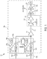
- FIG. 1 illustrates a circuit for processing received ultrasound signals, according to a non-limiting embodiment of the present application.
- the circuit 100 includes N ultrasonic transducers 102a... 102n, wherein N is an integer.
- the ultrasonic transducers are sensors in some embodiments, producing electrical signals representing received ultrasound signals.
- the ultrasonic transducers may also transmit ultrasound signals in some embodiments.
- the ultrasonic transducers may be capacitive micromachined ultrasonic transducers (CMUTs) in some embodiments.
- the ultrasonic transducers may be piezoelectric micromachined ultrasonic transducers (PMUTs) in some embodiments. Further alternative types of ultrasonic transducers may be used in other embodiments.
- the circuit 100 further comprises N circuitry channels 104a... 104n.
- the circuitry channels may correspond to a respective ultrasonic transducer 102a... 102n.
- the number of ultrasonic transducers 102a... 102n may be greater than the number of circuitry channels.
- the circuitry channels 104a... 104n may include transmit circuitry, receive circuitry, or both.
- the transmit circuitry may include transmit decoders 106a... 106n coupled to respective pulsers 108a... 108n.
- the pulsers 108a... 108n may control the respective ultrasonic transducers 102a... 102n to emit ultrasound signals.
- the receive circuitry of the circuitry channels 104a... 104n may receive the electrical signals output from respective ultrasonic transducers 102a... 102n.
- each circuitry channel 104a... 104n includes a respective receive switch 110a... 110n and an amplifier 112a... 112n.
- the receive switches 110a... 110n may be controlled to activate/deactivate readout of an electrical signal from a given ultrasonic transducer 102a... 102n. More generally, the receive switches 110a... 110n may be receive circuits, since alternatives to a switch may be employed to perform the same function.
- the amplifiers 112a... 112n, as well as amplifier 300 of FIG. 3 (described below), may be TIAs in some embodiments.
- One or more of the amplifiers 112a... 112n may be variable current amplifiers. As will be described further below, the current of the amplifiers may be varied during an acquisition period, thus adjusting the power consumption, noise level, and linearity of the amplifiers.
- the amplifiers 112a... 112n may output analog signals.
- the circuit 100 further comprises an averaging circuit 114, which is also referred to herein as a summer or a summing amplifier.
- the averaging circuit 114 is a buffer or an amplifier.
- the averaging circuit 114 may receive output signals from one or more of the amplifiers 112a... 112n and may provide an averaged output signal. The averaged output signal may be formed in part by adding or subtracting the signals from the various amplifiers 112a... 112n.
- the averaging circuit 114 may include a variable feedback resistance. The value of the variable feedback resistance may be adjusted dynamically based upon the number of amplifiers 112a... 112n from which the averaging circuit receives signals. In some embodiments, the variable resistance may include N resistance settings.
- variable resistance may have a number of resistance settings corresponding to the number of circuitry channels 104a... 104n.
- the average output signal may also be formed in part by application of the selected resistance to the combined signal received at the inputs of the averaging circuit 114.
- the averaging circuit 114 is coupled to an auto-zero block 116.
- the auto-zero block 116 is coupled to a programmable gain amplifier 118 which includes an attenuator 120 and a fixed gain amplifier 122.
- the programmable gain amplifier 118 is coupled to an ADC 126 via ADC drivers 124.
- the ADC drivers 124 include a first ADC driver 125a and a second ADC driver 125b.
- the ADC 126 digitizes the signal(s) from the averaging circuit 114.
- FIG. 1 illustrates a number of components as part of a circuit of an ultrasound device
- the various aspects described herein are not limited to the exact components or configuration of components illustrated.
- aspects of the present application relate to the amplifiers 112a... 112n, and the components illustrated downstream of those amplifiers in circuit 100 are optional in some embodiments.
- the components of FIG. 1 may be located on a single substrate or on different substrates.
- the ultrasonic transducers 102a... 102n may be on a first substrate 128a and the remaining illustrated components may be on a second substrate 128b.
- the first and/or second substrates may be semiconductor substrates, such as silicon substrates.
- the components of FIG. 1 may be on a single substrate.
- the ultrasonic transducers 102a... 102n and the illustrated circuitry may be monolithically integrated on the same semiconductor die. Such integration may be facilitated by using CMUTs as the ultrasonic transducers.
- the components of FIG. 1 form part of an ultrasound probe.
- the ultrasound probe may be handheld.
- the components of FIG. 1 form part of an ultrasound patch configured to be worn by a patient.
- FIG. 2 illustrates a non-limiting example of the amplifier 112a of FIG. 1 in greater detail. The same configuration may be used for the other amplifiers 112n of FIG. 1 .
- the ultrasonic transducer 102a and averaging circuit 114 are also illustrated, while for simplicity the receive switch 110a is omitted.
- the amplifier 112a is implemented as a two-stage operational amplifier ("op-amp" for short).
- the first stage 202 is coupled to the ultrasonic transducer 102a.
- the second stage 204 is coupled between the first stage 202 and the averaging circuit 114.
- the second stage 204 provides the output signal of the amplifier 112a, in this non-limiting example.
- the first stage 202 and second stage 204 each have a variable current source.
- the variable current source 203 is provided for the first stage 202 and sinks a current I1.
- the variable current source 205 is provided for the second stage 204 and sinks a current I2.
- the variable current sources 203 and 205 are illustrated as distinct from the respective stages 202 and 204, they may be considered part of the respective stages.
- the noise and linearity of the amplified signal may be controlled independently.
- the noise of the amplifier 112a is impacted primarily by the first stage 202.
- the linearity of the amplifier 112a is impacted primarily by the second stage 204. More generally, the same may be true for a multi-stage amplifier having two or more stages, such that the noise of the amplifier is impacted primarily by the first stage and the linearity of the amplifier is impacted primarily by the last stage.
- an acquisition period the noise and linearity of the amplified signal may vary in importance.
- the amplifier 112a of FIG. 2 is designed to allow for independent and variable control of noise and linearity.
- the control may be provided via the variable current sources 203 and 205.
- the variable current source 203 may be controlled to sink a relatively small amount of current, while the current source 205 may be controlled to sink a relatively large amount of current.
- the second stage 204 may operate to control the linearity of the amplified signal produced by the amplifier 112a, while the first stage 202 may control the noise of the amplified signal 202 to a lesser extent than that to which it is capable.
- the current sunk by the variable current source 203 may be increased while the current sunk by the variable current source 205 may be decreased.
- the first stage 202 may operate to control the noise of the amplifier 112a to a greater extent.
- the second stage 204 may operate to control the linearity of the amplifier 112a to a lesser extent.
- dynamic current biasing of the amplifier 112a, and first stage 202 and second stage 204 more specifically, may be implemented to control the power, noise, and linearity characteristics of the amplifier during an acquisition period.
- the dynamic control of current sources 203 and 205 may be achieved using a digital controller, an example being shown in FIG. 3A .
- the variable current sources 203 and 205 may each include two or more programmable current settings. The greater the number of settings, the greater the control over the current sunk by the current sources 203 and 205.
- the amplifier 112a also includes a variable feedback impedance 206.
- the variable feedback impedance is a variable RC feedback circuit.
- An example of the variable RC feedback circuit is illustrated in FIG. 3A and described in connection with that figure.
- the feedback impedance determines the transimpedance gain of the transimpedance amplifier, such that the input current signal may be converted into an output voltage of varying amplitude.
- an embodiment of the application provides a multi-stage TIA having two or more independently controllable variable current sources, with a variable feedback impedance.
- the variable current sources may allow for dynamic current biasing of the TIA, for example during an acquisition period.
- the power consumption, noise, and linearity of the amplifier may be adjusted during the acquisition period.
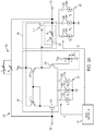
- FIG. 3A is a circuit diagram illustrating an implementation of the amplifier 112a of FIG. 2 , according to a non-limiting embodiment of the present application.
- the amplifier 300 has an input 302 and an output 304.
- the input 302 may be coupled to an ultrasonic transducer or a receive switch, as described previously in connection with FIGs. 1 and 2 , and may receive an electrical signal representing an ultrasound signal received by the ultrasonic transducer.
- the output 304 may provide an amplified output signal of the amplifier 112a, and may be coupled to an averaging circuit or other component to which it is desired to provide the amplified output signal.
- the amplifier 300 includes a first stage 306 and a second stage 308, which may be implementations of the first stage 202 and second stage 204 of FIG. 2 , respectively.
- the first stage 306 includes an NMOS transistor 310 having a gate configured to receive the signal at input 302.
- PMOS transistor 312 and PMOS transistor 314 have their gates coupled, with the drain of PMOS transistor 312 coupled to the drain of NMOS transistor 310.
- the gate of transistor 312 is coupled to its drain.
- Transistors 312 and 314 are also configured to receive a power supply voltage VDDA.
- the first stage 306 further comprises NMOS transistor 316 having a gate configured to receive a bias voltage provided by an RC circuit.
- the RC circuit includes two resistors, of value R, with a capacitor C b coupled in parallel with one of the resistors.
- the other resistor receives the power supply voltage VDDA.
- the drain of PMOS transistor 314 is coupled to the drain of NMOS transistor 316.
- An example value for R is 50 kOhm and an example value for C b is 10 pF, although alternatives for both are possible, such as +/- 20% of those values listed, or any value or range of values within such ranges.
- the second stage 308 includes a PMOS transistor 318 configured to receive the output of the first stage 306.
- the gate of PMOS transistor 318 is coupled to a node between transistors 314 and 316 of the first stage 306.
- the source of PMOS transistor 318 receives VDDA.
- a variable impedance circuit 320 is also provided in the second stage 308.
- the variable impedance circuit 320 includes a variable capacitor Cc in series with a variable resistor R Z , and thus is a variable RC circuit in this embodiment.
- Variable impedance circuit 320 may provide stable operation of the amplifier 300 when the gain of the amplifier, or the currents of the currents sources, are varied.
- variable impedance circuit may be provided to maintain stable operation of the amplifier 300 for all the current magnitudes sunk by the variable current sources 321 and 325. That is, the values of C C and R Z may be adjusted during operation of the amplifier 300 to account for the different current settings programmed by the digital controller 330
- variable current source is provided for each of the stages 306 and 308.
- the variable current source 321 for the first stage 306 includes three parallel connected current sources 322a, 322b, and 322c.
- Current source 322a sinks a current I A
- current source 322b sinks a current 2I A
- current source 322c sinks a current 4I A .
- the current sources 322a-322c are coupled to the first stage 306 by respective switches 324a, 324b, and 324c, which effectively provides 3 bits (8 states) of control of the current.
- the current I A may equal 100 microAmps or+/-20% of that value, or any value or range of values within such ranges, as examples.
- the variable current source 325 for the second stage 308 includes three parallel connected current sources 326a, 326b, and 326c.
- Current source 326a sinks a current I B
- current source 326b sinks a current 2I B
- current source 326c sinks a current 4I B .
- the current sources 326a-326c are coupled to the second stage 308 by respective switches 328a, 328b, and 328c, which effectively provides 3 bits (8 states) of control of the current.
- the current I B may equal 50 microAmps or+/-20% of that value, or any value or range of values within such ranges, as examples.
- variable current sources each include three parallel-coupled current sources
- variable current sources may be implemented in various manners, including alternative manners to those illustrated. For example, more or fewer than three current sources may be coupled in parallel to create a variable current source. Also, the magnitudes of the current sources may be different than those illustrated in FIG. 3A . Any suitable magnitudes may be provided to allow for operation over a desired range of currents.
- a digital controller 330 is provided to control operation of the variable current sources 321 and 325.
- the digital controller provides control signals to (digitally) program the currents of the variable current sources.
- the digital controller 330 provides one or more switching signals S1 to control operation of the switches 324a-324c, and one or more switching signals S2 to control operation of the switches 328a-328c.
- the amount of current sunk by the variable current sources may be varied independently during operation of the amplifier 300, for example during an acquisition period.
- the digital controller 330 decreases the current sunk by variable current source 325 during the acquisition period and increases the current sunk by variable current source 321 during the acquisition period through suitable operation of the switching signals S1 and S2.
- the digital controller 330 may be any suitable type of controller.
- the digital controller may include integrated circuitry.
- the digital controller 330 may include or be part of an application specific integrated circuit (ASIC).
- ASIC application specific integrated circuit
- the digital controller 330 may not be specific to the amplifier 300.
- a digital controller may be provided to control more than one component of the circuit of FIG. 1 , one of which may be the amplifiers 112a... 112n.
- the amplifier 300 further includes a variable feedback impedance 332 formed by variable capacitor C f and variable resistor R f .
- the capacitor C f and resistor R f may be coupled between the output 304 and the input 302, and may be in parallel with each other.
- the variable feedback impedance 332 may control the gain of the amplifier 300.
- the values of C f and R f may be adjusted to vary the amplifier's gain.
- variable feedback impedance 332 and the variable impedance circuit 320 may be controlled in any suitable manner.
- the digital controller 330 may set the values of the feedback impedances. However, alternatives manners of control may be used.
- first and second stages may include more, fewer, or different components than those illustrated.
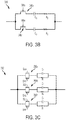
- FIG. 3B is a circuit diagram of an implementation of the variable impedance circuit 320 of FIG. 3A , according to a non-limiting embodiment of the present application.
- the variable impedance circuit 320 includes a number of switches 340a...340n configured in parallel and configured to receive respective control signals SWa...SWn.
- the digital controller 330 may provide the control signals SWa...SWn, although alternatives may be used.
- Each switch is coupled in series with a respective capacitor C C and resistor R Z .
- the impedance of the variable impedance circuit 320 may be adjusted during an acquisition period through suitable provision of the control signals SWa...SWn. Any suitable number of parallel signal paths may be provided, so that the illustrated example of two parallel signal paths is non-limiting.
- the number of parallel signal paths and the capacitance and resistive values provided may be selected to provide sufficient control of the feedback impedance to account for the variable operation of the amplifier across the range of operating scenarios resulting from the variation of the variable current sources. For example, for a given amplifier gain dictated by variable feedback impedance 332, appropriate settings of variable impedance circuit 320 may be selected. In some embodiments, a lookup table may be utilized to determine the appropriate settings of variable impedance circuit 320 based on a given gain set by variable feedback impedance 332.
- C C and R Z may be selected to provide desired operating characteristics.
- R Z may be equal to 3 kOhms in some embodiments, and C C may be equal to 300 fF.
- Alternatives for both are possible. For example, they may assume values within +/- 20% of those values listed, or any value or range of values within such ranges.
- FIG. 3C is a circuit diagram of an implementation of the variable impedance circuit 332 of FIG. 3A , according to a non-limiting embodiment of the present application.
- the variable impedance circuit 332 includes a number of complementary switches 350a, 350b...350n. Each switch receives respective control signals SLa, SLb...SLn and SHa, SHb...SHn.
- the control signals may be provided by the digital controller 330 in some embodiments, although alternatives may be used.
- the complementary switches are coupled to respective parallel-connected RC circuits C f , R f . While three complementary switches are shown in FIG. 3C , any suitable number may be provided to allow for sufficient control of the gain of the amplifier 300.
- C f and R f may be selected to provide desired operating characteristics.
- R f may be equal to 180 kOhms in some embodiments, and C f may be equal to 84 fF.
- Alternatives for both are possible. For example, they may assume values within +/- 20% of those values listed, or any value or range of values within such ranges.
- FIG. 4 is a graph illustrating the behavior of two variable current sources of a variable current amplifier during an acquisition period, as may be implemented by the amplifier of FIGs. 2 and 3A , which again may be a TIA.
- the illustrated behavior may be implemented by the variable current sources 203 and 205 of FIG. 2 .
- the x-axis represents time during an acquisition period, ranging from t0 to t8.
- the y-axis represents the current of the current source, having values ranging from I0 to I8.
- the values of t0-t8 and I0-18 may be any suitable values for operation of a given ultrasound system, as the various aspects described herein are not limited to implementation of any specific time or current values.
- the number of time intervals during an acquisition period is non-limiting, as more or fewer may be implemented.
- the number of current values which may be implemented is non-limiting, as more or fewer may be implemented.
- Curve 402 represents the current of a variable current source of a second stage of a variable current amplifier. Thus, curve 402 may represent the current of current source 205 of FIG. 2 .
- Curve 404 represents the current of a variable current source of a first stage of the variable current amplifier. Thus, curve 404 may represent the current of current source 203 of FIG. 2 .
- FIG. 4 illustrates that the currents of the first and second stages of the variable current amplifier move in opposing directions during the acquisition period. That is, curve 402 decreases moving from time t0 to time t8, while curve 404 increases during the same time.
- the first and second stages of the variable current amplifier may impact different characteristics of the variable current amplifier behavior, such as noise and linearity.
- the impact of the two stages of the variable current amplifier may vary during the acquisition period. That is, the impact of the second stage may be greater initially, up to time t4, while the impact of the first stage may be greater thereafter, from time t4 to time t8.
- the currents of the two stages of a two-stage op-amp being used to implement a variable current amplifier may be controlled by digital codes.
- the current values I 0-17 of FIG. 4 may correspond to different digital codes set by a digital controller, such as digital controller 330 of FIG. 3A .
- FIG. 4 illustrates that the currents in the first and second stages of the amplifier switch at the same times, not all embodiments are limited in this respect.
- the current in the second stage could be adjusted at times offset from those at which the current in the first stage is adjusted.
- the currents of the two stages need not be adjusted the same number of times during an acquisition period.
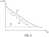
- an aspect of the present application provides an amplifier with a variable current source which is controlled to adjust the noise of the amplifier during an acquisition period.
- FIG. 5 illustrates an example of such operation.
- FIG. 5 the voltage of an electrical signal 502 output by an ultrasonic transducer, and thus representing a detected ultrasound signal, is illustrated as a function of time.
- Dashed line 504 represents the noise floor of an amplifier used to amplify the electrical signal 502, and may correspond to the noise floor of an amplifier of the types described herein, such as amplifier 112a.
- the noise floor of the amplifier is decreased.
- Such a decrease in the noise floor may be achieved by controlling the current sunk by a variable current source of the amplifier in the manner described previously herein.
- the variable current source 203 may be increased during the acquisition period to decrease the noise floor of the amplifier 112a.
- the noise floor may be adjusted to a level which provides an acceptable signal-to-noise ratio (SNR).
- SNR signal-to-noise ratio
- FIG. 5 also illustrates a constant noise floor 506. It can be seen that while the constant noise floor 506 is at the same level as dashed line 504 toward the end of the acquisition period, the constant noise floor 506 is lower than the value of the dashed line 504 up to that point. As has been described herein, the noise level of an amplifier may be dependent on the current consumed by the amplifier, and in such situations it should be appreciated that operating with a constant noise floor 506 requires significantly more current (and therefore power) than operating according to dashed line 504. Thus, aspects of the present application providing for a variable current amplifier to amplify ultrasound signals may provide substantial power savings compared to amplifiers operating with a constant noise level.
- the amount of power savings may be significant.
- the amplifiers 112a... 112n may consume a significant amount of power.
- the amplifiers 112a... 112n may consume more power than any other components of the circuit 100. Accordingly, reducing the power consumption of the amplifiers 112a... 112n may provide a significant reduction in power of the circuit 100.
- utilizing variable current amplifiers of the types described herein may provide up to a 25% power reduction, up to a 40% power reduction, up to a 50% power reduction, or any range or value within such ranges, in terms of the operation of the amplifier.
- the resulting power reduction for the circuit 100 may be up to 10%, up to 20%, up to 25%, or any range or value within such ranges.
- certain embodiments described herein have focused on two-stage amplifiers.
- the techniques described herein may apply to multi-stage amplifiers having two or more stages.
- the first stage may predominantly control the noise of the amplifier, while the last stage may predominantly control the linearity of the amplifier.
Landscapes
- Engineering & Computer Science (AREA)
- Health & Medical Sciences (AREA)
- Life Sciences & Earth Sciences (AREA)
- Power Engineering (AREA)
- Physics & Mathematics (AREA)
- Veterinary Medicine (AREA)
- Biophysics (AREA)
- Pathology (AREA)
- Public Health (AREA)
- Biomedical Technology (AREA)
- Heart & Thoracic Surgery (AREA)
- Medical Informatics (AREA)
- Molecular Biology (AREA)
- Surgery (AREA)
- Animal Behavior & Ethology (AREA)
- General Health & Medical Sciences (AREA)
- Computer Networks & Wireless Communication (AREA)
- General Physics & Mathematics (AREA)
- Radar, Positioning & Navigation (AREA)
- Remote Sensing (AREA)
- Radiology & Medical Imaging (AREA)
- Nuclear Medicine, Radiotherapy & Molecular Imaging (AREA)
- Amplifiers (AREA)
- Transducers For Ultrasonic Waves (AREA)
- Ultra Sonic Daignosis Equipment (AREA)
- Computer Vision & Pattern Recognition (AREA)
Applications Claiming Priority (2)
| Application Number | Priority Date | Filing Date | Title |
|---|---|---|---|
| US14/957,395 US10187020B2 (en) | 2015-12-02 | 2015-12-02 | Trans-impedance amplifier for ultrasound device and related apparatus and methods |
| PCT/US2016/064314 WO2017095981A1 (en) | 2015-12-02 | 2016-12-01 | Trans-impedance amplifier for ultrasound device and related apparatus and methods |
Publications (3)
| Publication Number | Publication Date |
|---|---|
| EP3384687A1 EP3384687A1 (en) | 2018-10-10 |
| EP3384687A4 EP3384687A4 (en) | 2019-07-03 |
| EP3384687B1 true EP3384687B1 (en) | 2021-06-02 |
Family
ID=58797744
Family Applications (1)
| Application Number | Title | Priority Date | Filing Date |
|---|---|---|---|
| EP16871463.2A Active EP3384687B1 (en) | 2015-12-02 | 2016-12-01 | Trans-impedance amplifier for ultrasound device and related apparatus and methods |
Country Status (10)
| Country | Link |
|---|---|
| US (5) | US10187020B2 (enExample) |
| EP (1) | EP3384687B1 (enExample) |
| JP (1) | JP6850293B2 (enExample) |
| KR (1) | KR20180089465A (enExample) |
| CN (1) | CN108370484B (enExample) |
| AU (2) | AU2016364736A1 (enExample) |
| CA (1) | CA3006064A1 (enExample) |
| ES (1) | ES2879688T3 (enExample) |
| TW (1) | TWI715688B (enExample) |
| WO (1) | WO2017095981A1 (enExample) |
Families Citing this family (27)
| Publication number | Priority date | Publication date | Assignee | Title |
|---|---|---|---|---|
| US9705518B2 (en) | 2015-12-02 | 2017-07-11 | Butterfly Network, Inc. | Asynchronous successive approximation analog-to-digital converter and related methods and apparatus |
| US10175347B2 (en) | 2015-12-02 | 2019-01-08 | Butterfly Network, Inc. | Ultrasound receiver circuitry and related apparatus and methods |
| US10187020B2 (en) | 2015-12-02 | 2019-01-22 | Butterfly Network, Inc. | Trans-impedance amplifier for ultrasound device and related apparatus and methods |
| US9492144B1 (en) | 2015-12-02 | 2016-11-15 | Butterfly Network, Inc. | Multi-level pulser and related apparatus and methods |
| US10082488B2 (en) | 2015-12-02 | 2018-09-25 | Butterfly Network, Inc. | Time gain compensation circuit and related apparatus and methods |
| US10624613B2 (en) | 2016-01-15 | 2020-04-21 | Butterfly Network, Inc. | Ultrasound signal processing circuitry and related apparatus and methods |
| US10009036B2 (en) * | 2016-09-09 | 2018-06-26 | Samsung Electronics Co., Ltd | System and method of calibrating input signal to successive approximation register (SAR) analog-to-digital converter (ADC) in ADC-assisted time-to-digital converter (TDC) |
| KR20200020798A (ko) * | 2017-06-20 | 2020-02-26 | 버터플라이 네트워크, 인크. | 초음파 디바이스를 위한 멀티-스테이지 트랜스-임피던스 증폭기(tia) |
| CA3066100A1 (en) * | 2017-06-20 | 2018-12-27 | Butterfly Network, Inc. | Amplifier with built in time gain compensation for ultrasound applications |
| CA3064584A1 (en) | 2017-06-20 | 2018-12-27 | Butterfly Network, Inc. | Single-ended trans-impedance amplifier (tia) for ultrasound device |
| EP3642960A4 (en) | 2017-06-20 | 2021-03-17 | Butterfly Network, Inc. | ANALOGUE-DIGITAL SIGNAL CONVERSION IN AN ULTRASONIC DEVICE |
| JP7128649B2 (ja) * | 2018-04-27 | 2022-08-31 | 富士フイルムヘルスケア株式会社 | 超音波診断装置、及びそれに用いる探触子 |
| JP2021522734A (ja) | 2018-05-03 | 2021-08-30 | バタフライ ネットワーク,インコーポレイテッド | Cmosセンサ上の超音波トランスデューサ用の圧力ポート |
| JP7128693B2 (ja) * | 2018-09-10 | 2022-08-31 | 富士フイルムヘルスケア株式会社 | 超音波診断装置、及びそれに用いる探触子 |
| TW202034624A (zh) | 2018-11-09 | 2020-09-16 | 美商蝴蝶網路公司 | 用於超音波裝置的跨阻抗放大器(tia) |
| CN110057921B (zh) * | 2019-04-11 | 2021-07-02 | 成都华芯微医疗科技有限公司 | 一种三维超声成像系统 |
| US11558062B2 (en) | 2019-07-25 | 2023-01-17 | Bfly Operations, Inc. | Methods and apparatuses for turning on and off an ADC driver in an ultrasound device |
| US11921240B2 (en) | 2019-09-19 | 2024-03-05 | Bfly Operations, Inc. | Symmetric receiver switch for ultrasound devices |
| JP2022550129A (ja) | 2019-09-27 | 2022-11-30 | ビーエフエルワイ オペレーションズ,インコーポレイテッド | 胎児心音及び子宮収縮信号を監視するための方法及び装置 |
| WO2021211822A1 (en) | 2020-04-16 | 2021-10-21 | Bfly Operations, Inc. | Methods and circuitry for built-in self-testing of circuitry and/or transducers in ultrasound devices |
| US11808897B2 (en) | 2020-10-05 | 2023-11-07 | Bfly Operations, Inc. | Methods and apparatuses for azimuthal summing of ultrasound data |
| FR3118549B1 (fr) * | 2020-12-28 | 2025-10-31 | Easii Ic | Amplificateur de transimpédance programmable |
| US11504093B2 (en) * | 2021-01-22 | 2022-11-22 | Exo Imaging, Inc. | Equalization for matrix based line imagers for ultrasound imaging systems |
| US12156762B2 (en) | 2021-04-01 | 2024-12-03 | Bfly Operations, Inc. | Apparatuses and methods for configuring ultrasound devices |
| WO2023133100A2 (en) * | 2022-01-04 | 2023-07-13 | Bfly Operations, Inc. | Ultrasound devices configured to change from default mode to power save mode and methods associated with the same |
| KR102404283B1 (ko) | 2022-02-15 | 2022-06-02 | (주)에프와이디 | 마이크로폰 센서용 리드아웃 회로 |
| CN117714940B (zh) * | 2024-02-05 | 2024-04-19 | 江西斐耳科技有限公司 | 一种aux功放链路底噪优化方法及系统 |
Family Cites Families (80)
| Publication number | Priority date | Publication date | Assignee | Title |
|---|---|---|---|---|
| US3274821A (en) | 1962-10-24 | 1966-09-27 | Automation Ind Inc | Ultrasonic testing apparatus having improved resolution |
| US3367173A (en) | 1964-02-21 | 1968-02-06 | Haffrel Instr Inc | Device for sonic and ultrasonic internal scanning of solid and fluid media |
| US3787803A (en) | 1972-11-29 | 1974-01-22 | Raytheon Co | High performance meter depth sounder for automatically indicating depth without manual adjustment |
| US4098130A (en) | 1977-03-11 | 1978-07-04 | General Electric Company | Energy reflection flaw detection system |
| US4512350A (en) | 1983-04-22 | 1985-04-23 | Irex Corporation | Time gain control signal generator for an ultrasonic diagnostic system |
| US4504747A (en) | 1983-11-10 | 1985-03-12 | Motorola, Inc. | Input buffer circuit for receiving multiple level input voltages |
| NL8600406A (nl) | 1986-02-18 | 1987-09-16 | Philips Nv | Automatisch geregeld versterkerstelsel. |
| JP2564133B2 (ja) * | 1987-04-17 | 1996-12-18 | オリンパス光学工業株式会社 | 固体撮像装置 |
| US5057719A (en) | 1990-06-27 | 1991-10-15 | Sverdrup Technology, Inc. | Passively forced current sharing among transistors |
| JP2543234B2 (ja) | 1990-06-29 | 1996-10-16 | 松下電器産業株式会社 | 超音波式物体感知装置 |
| JP3255303B2 (ja) * | 1992-08-31 | 2002-02-12 | ソニー株式会社 | 利得制御型増幅回路 |
| JPH0685585U (ja) | 1993-05-11 | 1994-12-06 | 吉晃 西村 | リモートコントロール装置 |
| US5622177A (en) | 1993-07-08 | 1997-04-22 | Siemens Aktiengesellschaft | Ultrasound imaging system having a reduced number of lines between the base unit and the probe |
| FR2726408B1 (fr) * | 1994-10-26 | 1996-11-29 | Suisse Electronique Microtech | Amplificateur transformateur d'impedance stable et a faible consommation |
| JP3418654B2 (ja) * | 1995-10-27 | 2003-06-23 | 株式会社日立製作所 | プリアンプ |
| US5942940A (en) | 1997-07-21 | 1999-08-24 | International Business Machines Corporation | Low voltage CMOS differential amplifier |
| JP3653171B2 (ja) | 1998-03-09 | 2005-05-25 | 株式会社リコー | 可変ゲイン増幅装置 |
| KR100416686B1 (ko) | 2000-10-12 | 2004-01-31 | 주식회사 메디슨 | 의료용 초음파 진단 시스템에 사용되는 집적된 고전압펄스 발생 회로 |
| US6404281B1 (en) * | 2000-11-14 | 2002-06-11 | Sirenza Microdevices, Inc. | Wide dynamic range transimpedance amplifier |
| US7313053B2 (en) | 2003-03-06 | 2007-12-25 | General Electric Company | Method and apparatus for controlling scanning of mosaic sensor array |
| US7176720B1 (en) | 2003-03-14 | 2007-02-13 | Cypress Semiconductor Corp. | Low duty cycle distortion differential to CMOS translator |
| US7691063B2 (en) | 2004-02-26 | 2010-04-06 | Siemens Medical Solutions Usa, Inc. | Receive circuit for minimizing channels in ultrasound imaging |
| US6937071B1 (en) | 2004-03-16 | 2005-08-30 | Micrel, Incorporated | High frequency differential power amplifier |
| US7451650B2 (en) * | 2004-08-27 | 2008-11-18 | General Electric Company | Systems and methods for adjusting gain within an ultrasound probe |
| US7888709B2 (en) | 2004-09-15 | 2011-02-15 | Sonetics Ultrasound, Inc. | Capacitive micromachined ultrasonic transducer and manufacturing method |
| US7265631B2 (en) * | 2005-03-12 | 2007-09-04 | Avago Technologies Ecbu Ip (Singapore) Pte. Ltd. | Transimpedance amplifier with signal amplification circuit that performs power signal regulation |
| US7256654B2 (en) | 2005-04-12 | 2007-08-14 | Raytheon Company | Amplifying a signal using a current shared power amplifier |
| JP4884018B2 (ja) * | 2005-05-12 | 2012-02-22 | パナソニック株式会社 | 増幅装置、および光ディスクドライブ装置 |
| EP1886098B1 (en) * | 2005-05-27 | 2016-03-09 | Expro Meters, Inc. | An apparatus and method for measuring a parameter of a multiphase flow |
| US7259628B2 (en) * | 2005-06-30 | 2007-08-21 | Silicon Laboratories Inc. | Signal dependent biasing scheme for an amplifier |
| US7449958B1 (en) * | 2005-08-17 | 2008-11-11 | Marvell International Ltd. | Open loop DC control for a transimpedance feedback amplifier |
| JP4880275B2 (ja) | 2005-10-03 | 2012-02-22 | オリンパスメディカルシステムズ株式会社 | 静電容量型超音波振動子装置 |
| US8465431B2 (en) | 2005-12-07 | 2013-06-18 | Siemens Medical Solutions Usa, Inc. | Multi-dimensional CMUT array with integrated beamformation |
| WO2008073140A2 (en) | 2006-05-15 | 2008-06-19 | Empirical Technologies Corporation | Wrist plethysmograph |
| JP2008042521A (ja) * | 2006-08-07 | 2008-02-21 | Matsushita Electric Ind Co Ltd | 電流グリッチ低減回路 |
| JP4991355B2 (ja) | 2007-03-14 | 2012-08-01 | 株式会社東芝 | 超音波診断装置及び超音波プローブ |
| US7605660B1 (en) * | 2007-11-12 | 2009-10-20 | Rf Micro Devices, Inc. | Linear multi-stage transimpedance amplifier |
| KR101024849B1 (ko) | 2007-12-04 | 2011-03-31 | 주식회사 하이볼릭 | 가변 이득 증폭기 |
| AU2009243918A1 (en) | 2008-05-07 | 2009-11-12 | Signostics Limited | Docking system for medical diagnostic scanning using a handheld device |
| US7733181B2 (en) * | 2008-05-23 | 2010-06-08 | Freescale Semiconductor, Inc. | Amplifier circuit having dynamically biased configuration |
| JP2010022761A (ja) | 2008-07-24 | 2010-02-04 | Ge Medical Systems Global Technology Co Llc | 超音波撮像装置 |
| JP4800352B2 (ja) | 2008-07-29 | 2011-10-26 | シャープ株式会社 | 自動利得制御回路、チューナ、テレビ受信機およびセットトップボックス |
| US7777522B2 (en) | 2008-07-31 | 2010-08-17 | Freescale Semiconductor, Inc. | Clocked single power supply level shifter |
| JP2010042146A (ja) | 2008-08-13 | 2010-02-25 | Ge Medical Systems Global Technology Co Llc | 超音波撮像装置 |
| ES2379410T3 (es) | 2008-10-14 | 2012-04-25 | Dolphiscan As | Aparato de tratamiento de imágenes por ultrasonido para leer y decodificar símbolos de matriz legibles por máquina |
| US8176787B2 (en) | 2008-12-17 | 2012-05-15 | General Electric Company | Systems and methods for operating a two-dimensional transducer array |
| JP5275830B2 (ja) | 2009-01-26 | 2013-08-28 | 富士フイルム株式会社 | 光超音波断層画像化装置および光超音波断層画像化方法 |
| JP5337523B2 (ja) | 2009-02-20 | 2013-11-06 | 株式会社日立製作所 | 半導体集積回路装置 |
| US8315125B2 (en) | 2009-03-18 | 2012-11-20 | Sonetics Ultrasound, Inc. | System and method for biasing CMUT elements |
| US8157738B2 (en) | 2009-06-02 | 2012-04-17 | Samplify Systems, Inc. | Ultrasound signal compression |
| US8207652B2 (en) | 2009-06-16 | 2012-06-26 | General Electric Company | Ultrasound transducer with improved acoustic performance |
| US8089309B2 (en) | 2009-06-26 | 2012-01-03 | Bae Systems Information And Electronic Systems Integration Inc. | Transimpedance amplifier input stage mixer |
| WO2011079880A1 (en) | 2009-12-30 | 2011-07-07 | Stmicroelectronics S.R.L. | Low voltage isolation switch, in particular for a transmission channel for ultrasound applications |
| US8891334B2 (en) | 2011-03-04 | 2014-11-18 | Georgia Tech Research Corporation | Compact, energy-efficient ultrasound imaging probes using CMUT arrays with integrated electronics |
| US8852103B2 (en) | 2011-10-17 | 2014-10-07 | Butterfly Network, Inc. | Transmissive imaging and related apparatus and methods |
| US9270273B2 (en) | 2011-10-28 | 2016-02-23 | Texas Instruments Incorporated | Level shifter |
| US8542037B2 (en) | 2012-01-23 | 2013-09-24 | Supertex, Inc. | Multi-level high voltage pulser integrated circuit using low voltage MOSFETs |
| JP5489144B1 (ja) | 2012-04-27 | 2014-05-14 | コニカミノルタ株式会社 | ビームフォーミング方法、及び超音波診断装置 |
| JP2013247536A (ja) | 2012-05-28 | 2013-12-09 | Sony Corp | 信号処理装置および方法、並びに通信装置 |
| US8766721B1 (en) | 2012-12-31 | 2014-07-01 | Texas Instruments Incorporated | Time gain compensation |
| JP6321980B2 (ja) * | 2013-03-09 | 2018-05-09 | キヤノン株式会社 | 検出回路、駆動方法、プローブ、及び被検体情報取得装置 |
| CA2903479C (en) | 2013-03-15 | 2023-10-10 | Butterfly Network, Inc. | Monolithic ultrasonic imaging devices, systems and methods |
| JP2014204195A (ja) | 2013-04-02 | 2014-10-27 | 富士通株式会社 | 利得制御回路、及び、超音波画像装置 |
| US9041453B2 (en) | 2013-04-04 | 2015-05-26 | Semiconductor Energy Laboratory Co., Ltd. | Pulse generation circuit and semiconductor device |
| EP3024594A2 (en) * | 2013-07-23 | 2016-06-01 | Butterfly Network Inc. | Interconnectable ultrasound transducer probes and related methods and apparatus |
| JP6093265B2 (ja) | 2013-08-07 | 2017-03-08 | ルネサスエレクトロニクス株式会社 | 半導体装置 |
| EP2849346B1 (en) | 2013-09-12 | 2019-08-21 | Socionext Inc. | Mixed-signal circuitry |
| CN103607130B (zh) | 2013-11-26 | 2016-01-13 | 徐州中矿大传动与自动化有限公司 | 基于fpga的dspace的三电平脉冲扩展的控制方法及其装置 |
| JP6205261B2 (ja) | 2013-12-13 | 2017-09-27 | ルネサスエレクトロニクス株式会社 | 半導体装置 |
| TWI671059B (zh) | 2014-04-18 | 2019-09-11 | 美商蝴蝶網路公司 | 超音波成像壓縮方法和設備 |
| CN106461767B (zh) | 2014-04-18 | 2019-05-28 | 蝴蝶网络有限公司 | 单衬底超声成像装置的架构、相关设备和方法 |
| US9705518B2 (en) | 2015-12-02 | 2017-07-11 | Butterfly Network, Inc. | Asynchronous successive approximation analog-to-digital converter and related methods and apparatus |
| US10175347B2 (en) | 2015-12-02 | 2019-01-08 | Butterfly Network, Inc. | Ultrasound receiver circuitry and related apparatus and methods |
| US9492144B1 (en) | 2015-12-02 | 2016-11-15 | Butterfly Network, Inc. | Multi-level pulser and related apparatus and methods |
| US9473136B1 (en) | 2015-12-02 | 2016-10-18 | Butterfly Network, Inc. | Level shifter and related methods and apparatus |
| US10187020B2 (en) | 2015-12-02 | 2019-01-22 | Butterfly Network, Inc. | Trans-impedance amplifier for ultrasound device and related apparatus and methods |
| US10082488B2 (en) | 2015-12-02 | 2018-09-25 | Butterfly Network, Inc. | Time gain compensation circuit and related apparatus and methods |
| US10624613B2 (en) | 2016-01-15 | 2020-04-21 | Butterfly Network, Inc. | Ultrasound signal processing circuitry and related apparatus and methods |
| US10231713B2 (en) | 2016-09-13 | 2019-03-19 | Butterfly Network, Inc. | Analog-to-digital drive circuitry having built-in time gain compensation functionality for ultrasound applications |
| TW202034624A (zh) | 2018-11-09 | 2020-09-16 | 美商蝴蝶網路公司 | 用於超音波裝置的跨阻抗放大器(tia) |
-
2015
- 2015-12-02 US US14/957,395 patent/US10187020B2/en active Active
-
2016
- 2016-12-01 KR KR1020187018520A patent/KR20180089465A/ko not_active Ceased
- 2016-12-01 CN CN201680070174.2A patent/CN108370484B/zh active Active
- 2016-12-01 JP JP2018528646A patent/JP6850293B2/ja active Active
- 2016-12-01 CA CA3006064A patent/CA3006064A1/en active Pending
- 2016-12-01 TW TW105139673A patent/TWI715688B/zh not_active IP Right Cessation
- 2016-12-01 AU AU2016364736A patent/AU2016364736A1/en not_active Abandoned
- 2016-12-01 EP EP16871463.2A patent/EP3384687B1/en active Active
- 2016-12-01 WO PCT/US2016/064314 patent/WO2017095981A1/en not_active Ceased
- 2016-12-01 ES ES16871463T patent/ES2879688T3/es active Active
-
2018
- 2018-11-01 US US16/178,117 patent/US11128267B2/en active Active
-
2021
- 2021-05-03 AU AU2021202768A patent/AU2021202768A1/en not_active Abandoned
- 2021-05-26 US US17/331,538 patent/US11863133B2/en active Active
-
2023
- 2023-12-20 US US18/389,875 patent/US12231097B2/en active Active
-
2025
- 2025-02-05 US US19/045,765 patent/US20250183859A1/en active Pending
Also Published As
| Publication number | Publication date |
|---|---|
| US20240120891A1 (en) | 2024-04-11 |
| ES2879688T3 (es) | 2021-11-22 |
| WO2017095981A1 (en) | 2017-06-08 |
| CN108370484B (zh) | 2020-10-16 |
| US20250183859A1 (en) | 2025-06-05 |
| CA3006064A1 (en) | 2017-06-08 |
| US12231097B2 (en) | 2025-02-18 |
| TW201739522A (zh) | 2017-11-16 |
| US20170163225A1 (en) | 2017-06-08 |
| EP3384687A4 (en) | 2019-07-03 |
| US10187020B2 (en) | 2019-01-22 |
| JP6850293B2 (ja) | 2021-03-31 |
| TWI715688B (zh) | 2021-01-11 |
| JP2019504540A (ja) | 2019-02-14 |
| AU2016364736A1 (en) | 2018-06-14 |
| US20210384872A1 (en) | 2021-12-09 |
| EP3384687A1 (en) | 2018-10-10 |
| AU2021202768A1 (en) | 2021-05-27 |
| US11128267B2 (en) | 2021-09-21 |
| CN108370484A (zh) | 2018-08-03 |
| US20190140603A1 (en) | 2019-05-09 |
| US11863133B2 (en) | 2024-01-02 |
| KR20180089465A (ko) | 2018-08-08 |
Similar Documents
| Publication | Publication Date | Title |
|---|---|---|
| EP3384687B1 (en) | Trans-impedance amplifier for ultrasound device and related apparatus and methods | |
| US11662447B2 (en) | Trans-impedance amplifier (TIA) for ultrasound devices | |
| US11545946B2 (en) | Amplifier with built in time gain compensation for ultrasound applications | |
| US11324484B2 (en) | Multi-stage trans-impedance amplifier (TIA) for an ultrasound device | |
| US10840864B2 (en) | Single-ended trans-impedance amplifier (TIA) for ultrasound device |
Legal Events
| Date | Code | Title | Description |
|---|---|---|---|
| STAA | Information on the status of an ep patent application or granted ep patent |
Free format text: STATUS: THE INTERNATIONAL PUBLICATION HAS BEEN MADE |
|
| PUAI | Public reference made under article 153(3) epc to a published international application that has entered the european phase |
Free format text: ORIGINAL CODE: 0009012 |
|
| STAA | Information on the status of an ep patent application or granted ep patent |
Free format text: STATUS: REQUEST FOR EXAMINATION WAS MADE |
|
| 17P | Request for examination filed |
Effective date: 20180607 |
|
| AK | Designated contracting states |
Kind code of ref document: A1 Designated state(s): AL AT BE BG CH CY CZ DE DK EE ES FI FR GB GR HR HU IE IS IT LI LT LU LV MC MK MT NL NO PL PT RO RS SE SI SK SM TR |
|
| AX | Request for extension of the european patent |
Extension state: BA ME |
|
| RIN1 | Information on inventor provided before grant (corrected) |
Inventor name: CASPER, ANDREW, J. Inventor name: FIFE, KEITH, G. Inventor name: CHEN, KAILIANG Inventor name: SANCHEZ, NEVADA, J. Inventor name: RALSTON, TYLER, S. |
|
| DAV | Request for validation of the european patent (deleted) | ||
| DAX | Request for extension of the european patent (deleted) | ||
| REG | Reference to a national code |
Ref country code: DE Ref legal event code: R079 Ref document number: 602016058965 Country of ref document: DE Free format text: PREVIOUS MAIN CLASS: H04R0031000000 Ipc: G01S0007520000 |
|
| A4 | Supplementary search report drawn up and despatched |
Effective date: 20190604 |
|
| RIC1 | Information provided on ipc code assigned before grant |
Ipc: G01S 7/52 20060101AFI20190528BHEP Ipc: H03F 3/45 20060101ALI20190528BHEP Ipc: H03F 1/08 20060101ALI20190528BHEP |
|
| GRAP | Despatch of communication of intention to grant a patent |
Free format text: ORIGINAL CODE: EPIDOSNIGR1 |
|
| STAA | Information on the status of an ep patent application or granted ep patent |
Free format text: STATUS: GRANT OF PATENT IS INTENDED |
|
| INTG | Intention to grant announced |
Effective date: 20210126 |
|
| GRAS | Grant fee paid |
Free format text: ORIGINAL CODE: EPIDOSNIGR3 |
|
| GRAA | (expected) grant |
Free format text: ORIGINAL CODE: 0009210 |
|
| STAA | Information on the status of an ep patent application or granted ep patent |
Free format text: STATUS: THE PATENT HAS BEEN GRANTED |
|
| RIN1 | Information on inventor provided before grant (corrected) |
Inventor name: CHEN, KAILIANG Inventor name: FIFE, KEITH, G. Inventor name: SANCHEZ, NEVADA, J. Inventor name: CASPER, ANDREW, J. Inventor name: RALSTON, TYLER, S. |
|
| REG | Reference to a national code |
Ref country code: CH Ref legal event code: EP |
|
| AK | Designated contracting states |
Kind code of ref document: B1 Designated state(s): AL AT BE BG CH CY CZ DE DK EE ES FI FR GB GR HR HU IE IS IT LI LT LU LV MC MK MT NL NO PL PT RO RS SE SI SK SM TR |
|
| REG | Reference to a national code |
Ref country code: GB Ref legal event code: FG4D |
|
| RIN1 | Information on inventor provided before grant (corrected) |
Inventor name: CHEN, KAILIANG Inventor name: FIFE, KEITH, G. Inventor name: SANCHEZ, NEVADA, J. Inventor name: CASPER, ANDREW, J. Inventor name: RALSTON, TYLER, S. |
|
| REG | Reference to a national code |
Ref country code: AT Ref legal event code: REF Ref document number: 1398972 Country of ref document: AT Kind code of ref document: T Effective date: 20210615 |
|
| REG | Reference to a national code |
Ref country code: IE Ref legal event code: FG4D |
|
| REG | Reference to a national code |
Ref country code: DE Ref legal event code: R096 Ref document number: 602016058965 Country of ref document: DE |
|
| REG | Reference to a national code |
Ref country code: LT Ref legal event code: MG9D |
|
| PG25 | Lapsed in a contracting state [announced via postgrant information from national office to epo] |
Ref country code: BG Free format text: LAPSE BECAUSE OF FAILURE TO SUBMIT A TRANSLATION OF THE DESCRIPTION OR TO PAY THE FEE WITHIN THE PRESCRIBED TIME-LIMIT Effective date: 20210902 Ref country code: HR Free format text: LAPSE BECAUSE OF FAILURE TO SUBMIT A TRANSLATION OF THE DESCRIPTION OR TO PAY THE FEE WITHIN THE PRESCRIBED TIME-LIMIT Effective date: 20210602 Ref country code: FI Free format text: LAPSE BECAUSE OF FAILURE TO SUBMIT A TRANSLATION OF THE DESCRIPTION OR TO PAY THE FEE WITHIN THE PRESCRIBED TIME-LIMIT Effective date: 20210602 Ref country code: LT Free format text: LAPSE BECAUSE OF FAILURE TO SUBMIT A TRANSLATION OF THE DESCRIPTION OR TO PAY THE FEE WITHIN THE PRESCRIBED TIME-LIMIT Effective date: 20210602 |
|
| REG | Reference to a national code |
Ref country code: NL Ref legal event code: MP Effective date: 20210602 |
|
| REG | Reference to a national code |
Ref country code: AT Ref legal event code: MK05 Ref document number: 1398972 Country of ref document: AT Kind code of ref document: T Effective date: 20210602 |
|
| REG | Reference to a national code |
Ref country code: ES Ref legal event code: FG2A Ref document number: 2879688 Country of ref document: ES Kind code of ref document: T3 Effective date: 20211122 |
|
| PG25 | Lapsed in a contracting state [announced via postgrant information from national office to epo] |
Ref country code: RS Free format text: LAPSE BECAUSE OF FAILURE TO SUBMIT A TRANSLATION OF THE DESCRIPTION OR TO PAY THE FEE WITHIN THE PRESCRIBED TIME-LIMIT Effective date: 20210602 Ref country code: SE Free format text: LAPSE BECAUSE OF FAILURE TO SUBMIT A TRANSLATION OF THE DESCRIPTION OR TO PAY THE FEE WITHIN THE PRESCRIBED TIME-LIMIT Effective date: 20210602 Ref country code: PL Free format text: LAPSE BECAUSE OF FAILURE TO SUBMIT A TRANSLATION OF THE DESCRIPTION OR TO PAY THE FEE WITHIN THE PRESCRIBED TIME-LIMIT Effective date: 20210602 Ref country code: NO Free format text: LAPSE BECAUSE OF FAILURE TO SUBMIT A TRANSLATION OF THE DESCRIPTION OR TO PAY THE FEE WITHIN THE PRESCRIBED TIME-LIMIT Effective date: 20210902 Ref country code: LV Free format text: LAPSE BECAUSE OF FAILURE TO SUBMIT A TRANSLATION OF THE DESCRIPTION OR TO PAY THE FEE WITHIN THE PRESCRIBED TIME-LIMIT Effective date: 20210602 Ref country code: GR Free format text: LAPSE BECAUSE OF FAILURE TO SUBMIT A TRANSLATION OF THE DESCRIPTION OR TO PAY THE FEE WITHIN THE PRESCRIBED TIME-LIMIT Effective date: 20210903 |
|
| PG25 | Lapsed in a contracting state [announced via postgrant information from national office to epo] |
Ref country code: RO Free format text: LAPSE BECAUSE OF FAILURE TO SUBMIT A TRANSLATION OF THE DESCRIPTION OR TO PAY THE FEE WITHIN THE PRESCRIBED TIME-LIMIT Effective date: 20210602 Ref country code: PT Free format text: LAPSE BECAUSE OF FAILURE TO SUBMIT A TRANSLATION OF THE DESCRIPTION OR TO PAY THE FEE WITHIN THE PRESCRIBED TIME-LIMIT Effective date: 20211004 Ref country code: NL Free format text: LAPSE BECAUSE OF FAILURE TO SUBMIT A TRANSLATION OF THE DESCRIPTION OR TO PAY THE FEE WITHIN THE PRESCRIBED TIME-LIMIT Effective date: 20210602 Ref country code: CZ Free format text: LAPSE BECAUSE OF FAILURE TO SUBMIT A TRANSLATION OF THE DESCRIPTION OR TO PAY THE FEE WITHIN THE PRESCRIBED TIME-LIMIT Effective date: 20210602 Ref country code: EE Free format text: LAPSE BECAUSE OF FAILURE TO SUBMIT A TRANSLATION OF THE DESCRIPTION OR TO PAY THE FEE WITHIN THE PRESCRIBED TIME-LIMIT Effective date: 20210602 Ref country code: AT Free format text: LAPSE BECAUSE OF FAILURE TO SUBMIT A TRANSLATION OF THE DESCRIPTION OR TO PAY THE FEE WITHIN THE PRESCRIBED TIME-LIMIT Effective date: 20210602 Ref country code: SK Free format text: LAPSE BECAUSE OF FAILURE TO SUBMIT A TRANSLATION OF THE DESCRIPTION OR TO PAY THE FEE WITHIN THE PRESCRIBED TIME-LIMIT Effective date: 20210602 Ref country code: SM Free format text: LAPSE BECAUSE OF FAILURE TO SUBMIT A TRANSLATION OF THE DESCRIPTION OR TO PAY THE FEE WITHIN THE PRESCRIBED TIME-LIMIT Effective date: 20210602 |
|
| REG | Reference to a national code |
Ref country code: DE Ref legal event code: R097 Ref document number: 602016058965 Country of ref document: DE |
|
| PLBE | No opposition filed within time limit |
Free format text: ORIGINAL CODE: 0009261 |
|
| STAA | Information on the status of an ep patent application or granted ep patent |
Free format text: STATUS: NO OPPOSITION FILED WITHIN TIME LIMIT |
|
| PG25 | Lapsed in a contracting state [announced via postgrant information from national office to epo] |
Ref country code: DK Free format text: LAPSE BECAUSE OF FAILURE TO SUBMIT A TRANSLATION OF THE DESCRIPTION OR TO PAY THE FEE WITHIN THE PRESCRIBED TIME-LIMIT Effective date: 20210602 |
|
| 26N | No opposition filed |
Effective date: 20220303 |
|
| PG25 | Lapsed in a contracting state [announced via postgrant information from national office to epo] |
Ref country code: AL Free format text: LAPSE BECAUSE OF FAILURE TO SUBMIT A TRANSLATION OF THE DESCRIPTION OR TO PAY THE FEE WITHIN THE PRESCRIBED TIME-LIMIT Effective date: 20210602 |
|
| PG25 | Lapsed in a contracting state [announced via postgrant information from national office to epo] |
Ref country code: MC Free format text: LAPSE BECAUSE OF FAILURE TO SUBMIT A TRANSLATION OF THE DESCRIPTION OR TO PAY THE FEE WITHIN THE PRESCRIBED TIME-LIMIT Effective date: 20210602 |
|
| REG | Reference to a national code |
Ref country code: CH Ref legal event code: PL |
|
| REG | Reference to a national code |
Ref country code: BE Ref legal event code: MM Effective date: 20211231 |
|
| PG25 | Lapsed in a contracting state [announced via postgrant information from national office to epo] |
Ref country code: LU Free format text: LAPSE BECAUSE OF NON-PAYMENT OF DUE FEES Effective date: 20211201 Ref country code: IE Free format text: LAPSE BECAUSE OF NON-PAYMENT OF DUE FEES Effective date: 20211201 |
|
| PG25 | Lapsed in a contracting state [announced via postgrant information from national office to epo] |
Ref country code: BE Free format text: LAPSE BECAUSE OF NON-PAYMENT OF DUE FEES Effective date: 20211231 |
|
| PG25 | Lapsed in a contracting state [announced via postgrant information from national office to epo] |
Ref country code: LI Free format text: LAPSE BECAUSE OF NON-PAYMENT OF DUE FEES Effective date: 20211231 Ref country code: CH Free format text: LAPSE BECAUSE OF NON-PAYMENT OF DUE FEES Effective date: 20211231 |
|
| PGFP | Annual fee paid to national office [announced via postgrant information from national office to epo] |
Ref country code: ES Payment date: 20230102 Year of fee payment: 7 |
|
| PG25 | Lapsed in a contracting state [announced via postgrant information from national office to epo] |
Ref country code: HU Free format text: LAPSE BECAUSE OF FAILURE TO SUBMIT A TRANSLATION OF THE DESCRIPTION OR TO PAY THE FEE WITHIN THE PRESCRIBED TIME-LIMIT; INVALID AB INITIO Effective date: 20161201 |
|
| PGFP | Annual fee paid to national office [announced via postgrant information from national office to epo] |
Ref country code: IT Payment date: 20221221 Year of fee payment: 7 |
|
| PG25 | Lapsed in a contracting state [announced via postgrant information from national office to epo] |
Ref country code: CY Free format text: LAPSE BECAUSE OF FAILURE TO SUBMIT A TRANSLATION OF THE DESCRIPTION OR TO PAY THE FEE WITHIN THE PRESCRIBED TIME-LIMIT Effective date: 20210602 |
|
| PG25 | Lapsed in a contracting state [announced via postgrant information from national office to epo] |
Ref country code: MK Free format text: LAPSE BECAUSE OF FAILURE TO SUBMIT A TRANSLATION OF THE DESCRIPTION OR TO PAY THE FEE WITHIN THE PRESCRIBED TIME-LIMIT Effective date: 20210602 |
|
| PG25 | Lapsed in a contracting state [announced via postgrant information from national office to epo] |
Ref country code: TR Free format text: LAPSE BECAUSE OF FAILURE TO SUBMIT A TRANSLATION OF THE DESCRIPTION OR TO PAY THE FEE WITHIN THE PRESCRIBED TIME-LIMIT Effective date: 20210602 |
|
| PG25 | Lapsed in a contracting state [announced via postgrant information from national office to epo] |
Ref country code: MT Free format text: LAPSE BECAUSE OF FAILURE TO SUBMIT A TRANSLATION OF THE DESCRIPTION OR TO PAY THE FEE WITHIN THE PRESCRIBED TIME-LIMIT Effective date: 20210602 |
|
| PGFP | Annual fee paid to national office [announced via postgrant information from national office to epo] |
Ref country code: GB Payment date: 20241227 Year of fee payment: 9 |
|
| PGFP | Annual fee paid to national office [announced via postgrant information from national office to epo] |
Ref country code: FR Payment date: 20241226 Year of fee payment: 9 |
|
| REG | Reference to a national code |
Ref country code: ES Ref legal event code: FD2A Effective date: 20250124 |
|
| PGFP | Annual fee paid to national office [announced via postgrant information from national office to epo] |
Ref country code: DE Payment date: 20241227 Year of fee payment: 9 |
|
| PG25 | Lapsed in a contracting state [announced via postgrant information from national office to epo] |
Ref country code: ES Free format text: LAPSE BECAUSE OF NON-PAYMENT OF DUE FEES Effective date: 20231202 |
|
| PG25 | Lapsed in a contracting state [announced via postgrant information from national office to epo] |
Ref country code: IT Free format text: LAPSE BECAUSE OF NON-PAYMENT OF DUE FEES Effective date: 20231201 |