EP3381245B1 - Gelötete verbindung für eine leiterplatte - Google Patents
Gelötete verbindung für eine leiterplatte Download PDFInfo
- Publication number
- EP3381245B1 EP3381245B1 EP16810543.5A EP16810543A EP3381245B1 EP 3381245 B1 EP3381245 B1 EP 3381245B1 EP 16810543 A EP16810543 A EP 16810543A EP 3381245 B1 EP3381245 B1 EP 3381245B1
- Authority
- EP
- European Patent Office
- Prior art keywords
- tapered
- interconnect
- compliant pin
- circuit board
- pcb
- Prior art date
- Legal status (The legal status is an assumption and is not a legal conclusion. Google has not performed a legal analysis and makes no representation as to the accuracy of the status listed.)
- Active
Links
Images



Classifications
-
- H—ELECTRICITY
- H01—ELECTRIC ELEMENTS
- H01R—ELECTRICALLY-CONDUCTIVE CONNECTIONS; STRUCTURAL ASSOCIATIONS OF A PLURALITY OF MUTUALLY-INSULATED ELECTRICAL CONNECTING ELEMENTS; COUPLING DEVICES; CURRENT COLLECTORS
- H01R12/00—Structural associations of a plurality of mutually-insulated electrical connecting elements, specially adapted for printed circuits, e.g. printed circuit boards [PCB], flat or ribbon cables, or like generally planar structures, e.g. terminal strips, terminal blocks; Coupling devices specially adapted for printed circuits, flat or ribbon cables, or like generally planar structures; Terminals specially adapted for contact with, or insertion into, printed circuits, flat or ribbon cables, or like generally planar structures
- H01R12/50—Fixed connections
- H01R12/51—Fixed connections for rigid printed circuits or like structures
- H01R12/55—Fixed connections for rigid printed circuits or like structures characterised by the terminals
- H01R12/58—Fixed connections for rigid printed circuits or like structures characterised by the terminals terminals for insertion into holes
-
- H—ELECTRICITY
- H01—ELECTRIC ELEMENTS
- H01R—ELECTRICALLY-CONDUCTIVE CONNECTIONS; STRUCTURAL ASSOCIATIONS OF A PLURALITY OF MUTUALLY-INSULATED ELECTRICAL CONNECTING ELEMENTS; COUPLING DEVICES; CURRENT COLLECTORS
- H01R12/00—Structural associations of a plurality of mutually-insulated electrical connecting elements, specially adapted for printed circuits, e.g. printed circuit boards [PCB], flat or ribbon cables, or like generally planar structures, e.g. terminal strips, terminal blocks; Coupling devices specially adapted for printed circuits, flat or ribbon cables, or like generally planar structures; Terminals specially adapted for contact with, or insertion into, printed circuits, flat or ribbon cables, or like generally planar structures
-
- H—ELECTRICITY
- H01—ELECTRIC ELEMENTS
- H01R—ELECTRICALLY-CONDUCTIVE CONNECTIONS; STRUCTURAL ASSOCIATIONS OF A PLURALITY OF MUTUALLY-INSULATED ELECTRICAL CONNECTING ELEMENTS; COUPLING DEVICES; CURRENT COLLECTORS
- H01R12/00—Structural associations of a plurality of mutually-insulated electrical connecting elements, specially adapted for printed circuits, e.g. printed circuit boards [PCB], flat or ribbon cables, or like generally planar structures, e.g. terminal strips, terminal blocks; Coupling devices specially adapted for printed circuits, flat or ribbon cables, or like generally planar structures; Terminals specially adapted for contact with, or insertion into, printed circuits, flat or ribbon cables, or like generally planar structures
- H01R12/70—Coupling devices
- H01R12/71—Coupling devices for rigid printing circuits or like structures
- H01R12/712—Coupling devices for rigid printing circuits or like structures co-operating with the surface of the printed circuit or with a coupling device exclusively provided on the surface of the printed circuit
- H01R12/714—Coupling devices for rigid printing circuits or like structures co-operating with the surface of the printed circuit or with a coupling device exclusively provided on the surface of the printed circuit with contacts abutting directly the printed circuit; Button contacts therefore provided on the printed circuit
-
- H—ELECTRICITY
- H01—ELECTRIC ELEMENTS
- H01R—ELECTRICALLY-CONDUCTIVE CONNECTIONS; STRUCTURAL ASSOCIATIONS OF A PLURALITY OF MUTUALLY-INSULATED ELECTRICAL CONNECTING ELEMENTS; COUPLING DEVICES; CURRENT COLLECTORS
- H01R12/00—Structural associations of a plurality of mutually-insulated electrical connecting elements, specially adapted for printed circuits, e.g. printed circuit boards [PCB], flat or ribbon cables, or like generally planar structures, e.g. terminal strips, terminal blocks; Coupling devices specially adapted for printed circuits, flat or ribbon cables, or like generally planar structures; Terminals specially adapted for contact with, or insertion into, printed circuits, flat or ribbon cables, or like generally planar structures
- H01R12/70—Coupling devices
- H01R12/71—Coupling devices for rigid printing circuits or like structures
- H01R12/712—Coupling devices for rigid printing circuits or like structures co-operating with the surface of the printed circuit or with a coupling device exclusively provided on the surface of the printed circuit
- H01R12/716—Coupling device provided on the PCB
-
- H—ELECTRICITY
- H01—ELECTRIC ELEMENTS
- H01R—ELECTRICALLY-CONDUCTIVE CONNECTIONS; STRUCTURAL ASSOCIATIONS OF A PLURALITY OF MUTUALLY-INSULATED ELECTRICAL CONNECTING ELEMENTS; COUPLING DEVICES; CURRENT COLLECTORS
- H01R13/00—Details of coupling devices of the kinds covered by groups H01R12/70 or H01R24/00 - H01R33/00
- H01R13/02—Contact members
- H01R13/04—Pins or blades for co-operation with sockets
- H01R13/05—Resilient pins or blades
-
- H—ELECTRICITY
- H01—ELECTRIC ELEMENTS
- H01R—ELECTRICALLY-CONDUCTIVE CONNECTIONS; STRUCTURAL ASSOCIATIONS OF A PLURALITY OF MUTUALLY-INSULATED ELECTRICAL CONNECTING ELEMENTS; COUPLING DEVICES; CURRENT COLLECTORS
- H01R13/00—Details of coupling devices of the kinds covered by groups H01R12/70 or H01R24/00 - H01R33/00
- H01R13/40—Securing contact members in or to a base or case; Insulating of contact members
- H01R13/405—Securing in non-demountable manner, e.g. moulding, riveting
-
- H—ELECTRICITY
- H01—ELECTRIC ELEMENTS
- H01R—ELECTRICALLY-CONDUCTIVE CONNECTIONS; STRUCTURAL ASSOCIATIONS OF A PLURALITY OF MUTUALLY-INSULATED ELECTRICAL CONNECTING ELEMENTS; COUPLING DEVICES; CURRENT COLLECTORS
- H01R13/00—Details of coupling devices of the kinds covered by groups H01R12/70 or H01R24/00 - H01R33/00
- H01R13/648—Protective earth or shield arrangements on coupling devices, e.g. anti-static shielding
- H01R13/652—Protective earth or shield arrangements on coupling devices, e.g. anti-static shielding with earth pin, blade or socket
-
- H—ELECTRICITY
- H05—ELECTRIC TECHNIQUES NOT OTHERWISE PROVIDED FOR
- H05K—PRINTED CIRCUITS; CASINGS OR CONSTRUCTIONAL DETAILS OF ELECTRIC APPARATUS; MANUFACTURE OF ASSEMBLAGES OF ELECTRICAL COMPONENTS
- H05K1/00—Printed circuits
- H05K1/02—Details
- H05K1/0213—Electrical arrangements not otherwise provided for
-
- H—ELECTRICITY
- H05—ELECTRIC TECHNIQUES NOT OTHERWISE PROVIDED FOR
- H05K—PRINTED CIRCUITS; CASINGS OR CONSTRUCTIONAL DETAILS OF ELECTRIC APPARATUS; MANUFACTURE OF ASSEMBLAGES OF ELECTRICAL COMPONENTS
- H05K1/00—Printed circuits
- H05K1/02—Details
- H05K1/0213—Electrical arrangements not otherwise provided for
- H05K1/0237—High frequency adaptations
-
- H—ELECTRICITY
- H05—ELECTRIC TECHNIQUES NOT OTHERWISE PROVIDED FOR
- H05K—PRINTED CIRCUITS; CASINGS OR CONSTRUCTIONAL DETAILS OF ELECTRIC APPARATUS; MANUFACTURE OF ASSEMBLAGES OF ELECTRICAL COMPONENTS
- H05K1/00—Printed circuits
- H05K1/02—Details
- H05K1/0296—Conductive pattern lay-out details not covered by sub groups H05K1/02 - H05K1/0295
- H05K1/0298—Multilayer circuits
-
- H—ELECTRICITY
- H05—ELECTRIC TECHNIQUES NOT OTHERWISE PROVIDED FOR
- H05K—PRINTED CIRCUITS; CASINGS OR CONSTRUCTIONAL DETAILS OF ELECTRIC APPARATUS; MANUFACTURE OF ASSEMBLAGES OF ELECTRICAL COMPONENTS
- H05K1/00—Printed circuits
- H05K1/02—Details
- H05K1/11—Printed elements for providing electric connections to or between printed circuits
-
- H—ELECTRICITY
- H05—ELECTRIC TECHNIQUES NOT OTHERWISE PROVIDED FOR
- H05K—PRINTED CIRCUITS; CASINGS OR CONSTRUCTIONAL DETAILS OF ELECTRIC APPARATUS; MANUFACTURE OF ASSEMBLAGES OF ELECTRICAL COMPONENTS
- H05K1/00—Printed circuits
- H05K1/02—Details
- H05K1/11—Printed elements for providing electric connections to or between printed circuits
- H05K1/111—Pads for surface mounting, e.g. lay-out
-
- H—ELECTRICITY
- H05—ELECTRIC TECHNIQUES NOT OTHERWISE PROVIDED FOR
- H05K—PRINTED CIRCUITS; CASINGS OR CONSTRUCTIONAL DETAILS OF ELECTRIC APPARATUS; MANUFACTURE OF ASSEMBLAGES OF ELECTRICAL COMPONENTS
- H05K1/00—Printed circuits
- H05K1/02—Details
- H05K1/11—Printed elements for providing electric connections to or between printed circuits
- H05K1/111—Pads for surface mounting, e.g. lay-out
- H05K1/112—Pads for surface mounting, e.g. lay-out directly combined with via connections
-
- H—ELECTRICITY
- H05—ELECTRIC TECHNIQUES NOT OTHERWISE PROVIDED FOR
- H05K—PRINTED CIRCUITS; CASINGS OR CONSTRUCTIONAL DETAILS OF ELECTRIC APPARATUS; MANUFACTURE OF ASSEMBLAGES OF ELECTRICAL COMPONENTS
- H05K1/00—Printed circuits
- H05K1/02—Details
- H05K1/11—Printed elements for providing electric connections to or between printed circuits
- H05K1/115—Via connections; Lands around holes or via connections
-
- H—ELECTRICITY
- H05—ELECTRIC TECHNIQUES NOT OTHERWISE PROVIDED FOR
- H05K—PRINTED CIRCUITS; CASINGS OR CONSTRUCTIONAL DETAILS OF ELECTRIC APPARATUS; MANUFACTURE OF ASSEMBLAGES OF ELECTRICAL COMPONENTS
- H05K1/00—Printed circuits
- H05K1/18—Printed circuits structurally associated with non-printed electric components
- H05K1/181—Printed circuits structurally associated with non-printed electric components associated with surface mounted components
-
- H—ELECTRICITY
- H05—ELECTRIC TECHNIQUES NOT OTHERWISE PROVIDED FOR
- H05K—PRINTED CIRCUITS; CASINGS OR CONSTRUCTIONAL DETAILS OF ELECTRIC APPARATUS; MANUFACTURE OF ASSEMBLAGES OF ELECTRICAL COMPONENTS
- H05K3/00—Apparatus or processes for manufacturing printed circuits
- H05K3/30—Assembling printed circuits with electric components, e.g. with resistors
- H05K3/306—Assembling printed circuits with electric components, e.g. with resistors with lead-in-hole components
- H05K3/308—Adaptations of leads
-
- H—ELECTRICITY
- H05—ELECTRIC TECHNIQUES NOT OTHERWISE PROVIDED FOR
- H05K—PRINTED CIRCUITS; CASINGS OR CONSTRUCTIONAL DETAILS OF ELECTRIC APPARATUS; MANUFACTURE OF ASSEMBLAGES OF ELECTRICAL COMPONENTS
- H05K3/00—Apparatus or processes for manufacturing printed circuits
- H05K3/30—Assembling printed circuits with electric components, e.g. with resistors
- H05K3/32—Assembling printed circuits with electric components, e.g. with resistors electrically connecting electric components or wires to printed circuits
- H05K3/34—Assembling printed circuits with electric components, e.g. with resistors electrically connecting electric components or wires to printed circuits by soldering
-
- H—ELECTRICITY
- H05—ELECTRIC TECHNIQUES NOT OTHERWISE PROVIDED FOR
- H05K—PRINTED CIRCUITS; CASINGS OR CONSTRUCTIONAL DETAILS OF ELECTRIC APPARATUS; MANUFACTURE OF ASSEMBLAGES OF ELECTRICAL COMPONENTS
- H05K3/00—Apparatus or processes for manufacturing printed circuits
- H05K3/30—Assembling printed circuits with electric components, e.g. with resistors
- H05K3/32—Assembling printed circuits with electric components, e.g. with resistors electrically connecting electric components or wires to printed circuits
- H05K3/34—Assembling printed circuits with electric components, e.g. with resistors electrically connecting electric components or wires to printed circuits by soldering
- H05K3/341—Surface mounted components
- H05K3/3421—Leaded components
-
- H—ELECTRICITY
- H05—ELECTRIC TECHNIQUES NOT OTHERWISE PROVIDED FOR
- H05K—PRINTED CIRCUITS; CASINGS OR CONSTRUCTIONAL DETAILS OF ELECTRIC APPARATUS; MANUFACTURE OF ASSEMBLAGES OF ELECTRICAL COMPONENTS
- H05K3/00—Apparatus or processes for manufacturing printed circuits
- H05K3/40—Forming printed elements for providing electric connections to or between printed circuits
- H05K3/42—Plated through-holes or plated via connections
-
- H—ELECTRICITY
- H01—ELECTRIC ELEMENTS
- H01R—ELECTRICALLY-CONDUCTIVE CONNECTIONS; STRUCTURAL ASSOCIATIONS OF A PLURALITY OF MUTUALLY-INSULATED ELECTRICAL CONNECTING ELEMENTS; COUPLING DEVICES; CURRENT COLLECTORS
- H01R12/00—Structural associations of a plurality of mutually-insulated electrical connecting elements, specially adapted for printed circuits, e.g. printed circuit boards [PCB], flat or ribbon cables, or like generally planar structures, e.g. terminal strips, terminal blocks; Coupling devices specially adapted for printed circuits, flat or ribbon cables, or like generally planar structures; Terminals specially adapted for contact with, or insertion into, printed circuits, flat or ribbon cables, or like generally planar structures
- H01R12/50—Fixed connections
- H01R12/51—Fixed connections for rigid printed circuits or like structures
- H01R12/52—Fixed connections for rigid printed circuits or like structures connecting to other rigid printed circuits or like structures
- H01R12/526—Fixed connections for rigid printed circuits or like structures connecting to other rigid printed circuits or like structures the printed circuits being on the same board
-
- H—ELECTRICITY
- H01—ELECTRIC ELEMENTS
- H01R—ELECTRICALLY-CONDUCTIVE CONNECTIONS; STRUCTURAL ASSOCIATIONS OF A PLURALITY OF MUTUALLY-INSULATED ELECTRICAL CONNECTING ELEMENTS; COUPLING DEVICES; CURRENT COLLECTORS
- H01R4/00—Electrically-conductive connections between two or more conductive members in direct contact, i.e. touching one another; Means for effecting or maintaining such contact; Electrically-conductive connections having two or more spaced connecting locations for conductors and using contact members penetrating insulation
- H01R4/02—Soldered or welded connections
- H01R4/028—Soldered or welded connections comprising means for preventing flowing or wicking of solder or flux in parts not desired
-
- H—ELECTRICITY
- H05—ELECTRIC TECHNIQUES NOT OTHERWISE PROVIDED FOR
- H05K—PRINTED CIRCUITS; CASINGS OR CONSTRUCTIONAL DETAILS OF ELECTRIC APPARATUS; MANUFACTURE OF ASSEMBLAGES OF ELECTRICAL COMPONENTS
- H05K1/00—Printed circuits
- H05K1/18—Printed circuits structurally associated with non-printed electric components
- H05K1/182—Printed circuits structurally associated with non-printed electric components associated with components mounted in printed circuit boards [PCB], e.g. insert-mounted components [IMC]
- H05K1/184—Printed circuits structurally associated with non-printed electric components associated with components mounted in printed circuit boards [PCB], e.g. insert-mounted components [IMC] associated with components inserted in holes through the PCBs and wherein terminals of the components are connected to printed contacts on the walls of the holes or at the edges thereof or protruding over or into the holes
-
- H—ELECTRICITY
- H05—ELECTRIC TECHNIQUES NOT OTHERWISE PROVIDED FOR
- H05K—PRINTED CIRCUITS; CASINGS OR CONSTRUCTIONAL DETAILS OF ELECTRIC APPARATUS; MANUFACTURE OF ASSEMBLAGES OF ELECTRICAL COMPONENTS
- H05K2201/00—Indexing scheme relating to printed circuits covered by H05K1/00
- H05K2201/09—Shape and layout
- H05K2201/09209—Shape and layout details of conductors
- H05K2201/09372—Pads and lands
- H05K2201/09472—Recessed pad for surface mounting; Recessed electrode of component
-
- H—ELECTRICITY
- H05—ELECTRIC TECHNIQUES NOT OTHERWISE PROVIDED FOR
- H05K—PRINTED CIRCUITS; CASINGS OR CONSTRUCTIONAL DETAILS OF ELECTRIC APPARATUS; MANUFACTURE OF ASSEMBLAGES OF ELECTRICAL COMPONENTS
- H05K2201/00—Indexing scheme relating to printed circuits covered by H05K1/00
- H05K2201/09—Shape and layout
- H05K2201/09209—Shape and layout details of conductors
- H05K2201/095—Conductive through-holes or vias
- H05K2201/09509—Blind vias, i.e. vias having one side closed
-
- H—ELECTRICITY
- H05—ELECTRIC TECHNIQUES NOT OTHERWISE PROVIDED FOR
- H05K—PRINTED CIRCUITS; CASINGS OR CONSTRUCTIONAL DETAILS OF ELECTRIC APPARATUS; MANUFACTURE OF ASSEMBLAGES OF ELECTRICAL COMPONENTS
- H05K2201/00—Indexing scheme relating to printed circuits covered by H05K1/00
- H05K2201/09—Shape and layout
- H05K2201/09209—Shape and layout details of conductors
- H05K2201/095—Conductive through-holes or vias
- H05K2201/09545—Plated through-holes or blind vias without lands
-
- H—ELECTRICITY
- H05—ELECTRIC TECHNIQUES NOT OTHERWISE PROVIDED FOR
- H05K—PRINTED CIRCUITS; CASINGS OR CONSTRUCTIONAL DETAILS OF ELECTRIC APPARATUS; MANUFACTURE OF ASSEMBLAGES OF ELECTRICAL COMPONENTS
- H05K2201/00—Indexing scheme relating to printed circuits covered by H05K1/00
- H05K2201/09—Shape and layout
- H05K2201/09818—Shape or layout details not covered by a single group of H05K2201/09009 - H05K2201/09809
- H05K2201/09827—Tapered, e.g. tapered hole, via or groove
-
- H—ELECTRICITY
- H05—ELECTRIC TECHNIQUES NOT OTHERWISE PROVIDED FOR
- H05K—PRINTED CIRCUITS; CASINGS OR CONSTRUCTIONAL DETAILS OF ELECTRIC APPARATUS; MANUFACTURE OF ASSEMBLAGES OF ELECTRICAL COMPONENTS
- H05K2201/00—Indexing scheme relating to printed circuits covered by H05K1/00
- H05K2201/10—Details of components or other objects attached to or integrated in a printed circuit board
- H05K2201/10007—Types of components
- H05K2201/10098—Components for radio transmission, e.g. radio frequency identification [RFID] tag, printed or non-printed antennas
-
- H—ELECTRICITY
- H05—ELECTRIC TECHNIQUES NOT OTHERWISE PROVIDED FOR
- H05K—PRINTED CIRCUITS; CASINGS OR CONSTRUCTIONAL DETAILS OF ELECTRIC APPARATUS; MANUFACTURE OF ASSEMBLAGES OF ELECTRICAL COMPONENTS
- H05K2201/00—Indexing scheme relating to printed circuits covered by H05K1/00
- H05K2201/10—Details of components or other objects attached to or integrated in a printed circuit board
- H05K2201/10007—Types of components
- H05K2201/10189—Non-printed connector
-
- H—ELECTRICITY
- H05—ELECTRIC TECHNIQUES NOT OTHERWISE PROVIDED FOR
- H05K—PRINTED CIRCUITS; CASINGS OR CONSTRUCTIONAL DETAILS OF ELECTRIC APPARATUS; MANUFACTURE OF ASSEMBLAGES OF ELECTRICAL COMPONENTS
- H05K2201/00—Indexing scheme relating to printed circuits covered by H05K1/00
- H05K2201/10—Details of components or other objects attached to or integrated in a printed circuit board
- H05K2201/10227—Other objects, e.g. metallic pieces
- H05K2201/10295—Metallic connector elements partly mounted in a hole of the PCB
-
- H—ELECTRICITY
- H05—ELECTRIC TECHNIQUES NOT OTHERWISE PROVIDED FOR
- H05K—PRINTED CIRCUITS; CASINGS OR CONSTRUCTIONAL DETAILS OF ELECTRIC APPARATUS; MANUFACTURE OF ASSEMBLAGES OF ELECTRICAL COMPONENTS
- H05K2201/00—Indexing scheme relating to printed circuits covered by H05K1/00
- H05K2201/10—Details of components or other objects attached to or integrated in a printed circuit board
- H05K2201/10613—Details of electrical connections of non-printed components, e.g. special leads
- H05K2201/10742—Details of leads
- H05K2201/1075—Shape details
- H05K2201/1078—Leads having locally deformed portion, e.g. for retention
-
- H—ELECTRICITY
- H05—ELECTRIC TECHNIQUES NOT OTHERWISE PROVIDED FOR
- H05K—PRINTED CIRCUITS; CASINGS OR CONSTRUCTIONAL DETAILS OF ELECTRIC APPARATUS; MANUFACTURE OF ASSEMBLAGES OF ELECTRICAL COMPONENTS
- H05K2201/00—Indexing scheme relating to printed circuits covered by H05K1/00
- H05K2201/10—Details of components or other objects attached to or integrated in a printed circuit board
- H05K2201/10613—Details of electrical connections of non-printed components, e.g. special leads
- H05K2201/10742—Details of leads
- H05K2201/1075—Shape details
- H05K2201/10803—Tapered leads, i.e. leads having changing width or diameter
-
- H—ELECTRICITY
- H05—ELECTRIC TECHNIQUES NOT OTHERWISE PROVIDED FOR
- H05K—PRINTED CIRCUITS; CASINGS OR CONSTRUCTIONAL DETAILS OF ELECTRIC APPARATUS; MANUFACTURE OF ASSEMBLAGES OF ELECTRICAL COMPONENTS
- H05K2201/00—Indexing scheme relating to printed circuits covered by H05K1/00
- H05K2201/10—Details of components or other objects attached to or integrated in a printed circuit board
- H05K2201/10613—Details of electrical connections of non-printed components, e.g. special leads
- H05K2201/10742—Details of leads
- H05K2201/1075—Shape details
- H05K2201/10871—Leads having an integral insert stop
-
- H—ELECTRICITY
- H05—ELECTRIC TECHNIQUES NOT OTHERWISE PROVIDED FOR
- H05K—PRINTED CIRCUITS; CASINGS OR CONSTRUCTIONAL DETAILS OF ELECTRIC APPARATUS; MANUFACTURE OF ASSEMBLAGES OF ELECTRICAL COMPONENTS
- H05K2201/00—Indexing scheme relating to printed circuits covered by H05K1/00
- H05K2201/10—Details of components or other objects attached to or integrated in a printed circuit board
- H05K2201/10613—Details of electrical connections of non-printed components, e.g. special leads
- H05K2201/10742—Details of leads
- H05K2201/1075—Shape details
- H05K2201/10878—Means for retention of a lead in a hole
-
- H—ELECTRICITY
- H05—ELECTRIC TECHNIQUES NOT OTHERWISE PROVIDED FOR
- H05K—PRINTED CIRCUITS; CASINGS OR CONSTRUCTIONAL DETAILS OF ELECTRIC APPARATUS; MANUFACTURE OF ASSEMBLAGES OF ELECTRICAL COMPONENTS
- H05K2201/00—Indexing scheme relating to printed circuits covered by H05K1/00
- H05K2201/10—Details of components or other objects attached to or integrated in a printed circuit board
- H05K2201/10613—Details of electrical connections of non-printed components, e.g. special leads
- H05K2201/10742—Details of leads
- H05K2201/10886—Other details
- H05K2201/10901—Lead partly inserted in hole or via
-
- H—ELECTRICITY
- H05—ELECTRIC TECHNIQUES NOT OTHERWISE PROVIDED FOR
- H05K—PRINTED CIRCUITS; CASINGS OR CONSTRUCTIONAL DETAILS OF ELECTRIC APPARATUS; MANUFACTURE OF ASSEMBLAGES OF ELECTRICAL COMPONENTS
- H05K2203/00—Indexing scheme relating to apparatus or processes for manufacturing printed circuits covered by H05K3/00
- H05K2203/04—Soldering or other types of metallurgic bonding
- H05K2203/0455—PTH for surface mount device [SMD], e.g. wherein solder flows through the PTH during mounting
-
- H—ELECTRICITY
- H05—ELECTRIC TECHNIQUES NOT OTHERWISE PROVIDED FOR
- H05K—PRINTED CIRCUITS; CASINGS OR CONSTRUCTIONAL DETAILS OF ELECTRIC APPARATUS; MANUFACTURE OF ASSEMBLAGES OF ELECTRICAL COMPONENTS
- H05K3/00—Apparatus or processes for manufacturing printed circuits
- H05K3/40—Forming printed elements for providing electric connections to or between printed circuits
- H05K3/42—Plated through-holes or plated via connections
- H05K3/421—Blind plated via connections
-
- Y—GENERAL TAGGING OF NEW TECHNOLOGICAL DEVELOPMENTS; GENERAL TAGGING OF CROSS-SECTIONAL TECHNOLOGIES SPANNING OVER SEVERAL SECTIONS OF THE IPC; TECHNICAL SUBJECTS COVERED BY FORMER USPC CROSS-REFERENCE ART COLLECTIONS [XRACs] AND DIGESTS
- Y02—TECHNOLOGIES OR APPLICATIONS FOR MITIGATION OR ADAPTATION AGAINST CLIMATE CHANGE
- Y02P—CLIMATE CHANGE MITIGATION TECHNOLOGIES IN THE PRODUCTION OR PROCESSING OF GOODS
- Y02P70/00—Climate change mitigation technologies in the production process for final industrial or consumer products
- Y02P70/50—Manufacturing or production processes characterised by the final manufactured product
Definitions
- the present invention generally relates to a printed circuit board and an electrical interconnect assembly.
- electronic components may be mounted on a printed circuit board (PCB) using a through-hole technique or surface-mount technique.
- a through hole technique a plurality of holes are drilled on one surface of the PCB.
- the holes are designed to pass through all layers of the PCB to the other surface of the PCB.
- the electronic components contain pins for coupling the electronic components to the PCB.
- the pins fit into a plurality of holes, trimmed on the opposite side of the PCB, and are soldered in place. Accordingly, using the through hole technique, components are typically placed on one side of the PCB.
- the electronic devices are directly mounted on a surface of the PCB.
- the devices are soldered directly onto the PCB.
- the surface-mount technique eliminates the need to drill holes on the PCB and allows for much smaller components to be coupled to the PCB.
- components can be mounted on both sides of the PCB.
- Fretting refers to the wear that occurs between two surfaces that are in contact with each other under a load. Fretting is particularly prevalent in the presence of vibration, which is an important concern for high-vibration environments, such as a circuit board mounted in vehicles used in rough terrains, airplanes or missiles.
- a PCB comprising a tapered surface interconnect with straight walls and a straight bottom surface and a compatible pin connector are known from WO 2009/057614 A1 . Further comparable PCBs are known from US 2011/061910 A1 , US 6 146 156 A , and US 2002/195271 A1 .
- the present invention refers to a printed circuit board according to claim 1.
- the at least one tapered surface interconnect includes a radial inclination taper section, with the radial inclination taper section being concave.
- the at least one tapered surface interconnect has a flared entrance aperture.
- the invention further refers to an electrical interconnect assembly according to claim 4 . Preferred embodiments of the invention are defined in the appended dependent claims.
- Embodiments of the present invention may provide a tapered surface interconnect formed on a printed circuit board (PCB).
- a compliant pin of an electrical connector may be coupled to the tapered surface interconnect and soldered thereto.
- the surface interconnect is formed by mechanical drilling through one or more layers of the PCB. According to various embodiments, the surface interconnect is not a through hole. That is, a depth of the surface interconnect is shorter than a height or a thickness of the PCB.
- the surface interconnect has a tapered side wall to allow for a better fit with a tapered compliant pin.
- the tapered surface interconnect includes a radial, i.e. concave, taper section. The bottom of the tapered surface interconnect may be rounded, flat, and/or pointed.
- the compliant pin may be soldered in place upon being coupled to the tapered surface interconnect.
- the tapered surface interconnect and tapered compliant pin assembly may provide up to 20 decibels (dB) reduction in crosstalk due to the tuned
- Figure 1 illustrates exemplary electrical interconnects 104, 106, 108 coupled to an exemplary printed circuit board (PCB) 102.
- the PCB 102 includes a plurality of surface interconnects 120, 122, 124.
- the surface interconnects 120, 122, 124 are drilled onto PCB 102.
- Each surface interconnect 120, 122, 124 is sized and configured to accept therein a compliant pin 114, 116, 118 of the electrical interconnects 104, 106, 108, respectively.
- the surface interconnects 120, 122, 124 may have tapered side walls to create a better fit between the surface interconnect and the compliant pin. The improved fit may have significant impact on electrical cross talk reduction.
- the compliant pins 114, 116, 118 of the electrical interconnects 104, 106, 108 may be soldered in place after being coupled to the surface interconnects 120, 122, 124 of the PCB 102.
- the surface interconnects 120, 122, 124 may be sized and configured to accept a portion of the solder therein.
- the surface interconnects may be drilled through one or more layers of the PCB.
- the surface interconnects may not be through holes that extend through an entire thickness, i.e. the height, of the PCB.
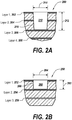
- Figures 2A-2B illustrate exemplary surface interconnects formed on a PCB according to various examples not corresponding to the invention as defined in the claims but useful for the understanding thereof.
- Figure 2A illustrates an exemplary multi-layer PCB 200.
- PCB 200 may have at least four layers 202, 204, 206, 208.
- the surface interconnect 210 may be drilled up to the third layer 206 of PCB 200.
- the surface interconnect 210 may have a depth 212 substantially equivalent to a height of the first two layers 202, 204 of the PCB 200.
- the surface interconnect 210 may have a depth 212 of up to 0.05 pinches (1.27mm).
- the surface interconnect 210 may have a tapered side wall 216.
- the side wall 216 may have at least one of no inclination, a linear inclination up to 15°, and a concave inclination.
- the side wall 216 may a flared entrance aperture.
- a width of the surface opening 214 of the surface interconnect 210 provided at the top layer 202 of the PCB 200 may be up to 0.05 inches (1.27 mm).
- Figure 2B illustrates another exemplary multi-layer PCB 250. As provided above the surface interconnect may be drilled through one layer of a multilayer PCB. For example, the PCB may have at least three layers 252, 254, 256.
- the surface interconnect 260 may be drilled up to the second layer 256 of the PCB 250.
- the surface interconnect 260 may have a depth 262 substantially equivalent to a height of the first layer 252 of PCB 250.
- the surface interconnect 260 may have a depth 262 of up to 0.05 inches (1.27 mm).
- the surface interconnect 260 may have tapered side wall 266.
- the side wall 266 may have at least one of no inclination, a linear inclination up to 15°, and a concave inclination.
- the side wall 216 may a flared entrance aperture.
- a width of the surface opening 264 of the surface interconnect 260 provided at the top layer 252 of PCB 250 may be as small as 0.004 pinches (0.1016 mm) and up to 0.035 inches (0.889 mm).
- Figure 3 illustrates an exemplary electrical connector 304 coupled and soldered to an exemplary PCB 302 according to an illustrative example not belonging to the invention as defined in the claims but useful for the understanding thereof.
- the compliant pin coupled to the tapered surface interconnect may be soldered thereto.
- the electrical connector 304 may include a compliant pin 314 formed at a distal end 310 thereof.
- the electrical connector 304 may be coupled to the PCB 302 by inserting the compliant pin 314 inside a surface interconnect 306 drilled on the surface of the PCB 302.
- the surface interconnect 306 may have tapered side wall 308 to create a better fit between the surface interconnect 306 and the compliant pin 314.
- FIGS 4A-4F illustrate some exemplary configurations for the compliant pin and surface interconnect geometries.
- the compliant pin of the electrical connector and the surface interconnect of the PCB may have various configurations.
- One of ordinary skill in the art would appreciate that the shown configurations are illustrative purposes only and should not be construed as limiting.
- Figure 4A illustrates an electrical connector 404 with a compliant pin 414 that is not in direct physical contact with a bottom surface 406 of the surface interconnect 405.
- the surface interconnect 405 may be formed by drilling into one or more layers of the PCB 402.
- the compliant pin 414 may have a tapered side wall 416.
- the surface interconnect 405 may also have a tapered side wall 408.
- a taper angle of the tapered side wall 416 of the compliant pin 414 may be substantially equal to a taper angle of the tapered side wall 408 of the surface interconnect 405.
- the compliant pin 414 maybe soldered in place upon being coupled to, i.e. inserted within, the surface interconnect 405.
- the solder 418 may be provided within the surface interconnect 405 to fill the gap between the compliant pin 414 and the surface interconnect 405.
- the soldered assembly may be reliably used in rugged applications. Even during extreme vibration, the soldered assembly may prevent the electrical interconnect 404 from decoupling from the PCB 402.
- Figure 4B illustrates an electrical connector 424 with a compliant pin 434.
- the compliant pin 434 is sized and dimensioned to be in substantially direct physical and electrical contact with a bottom surface 426 of the surface interconnect 425.
- the surface interconnect 425 may be formed by drilling into one or more layers of the PCB 422.
- the compliant pin 434 may have a tapered side wall 436.
- the surface interconnect 425 may also have a tapered side wall 428.
- a taper angle of the tapered side wall 436 of the compliant pin 434 may be substantially equal to a taper angle of the tapered side wall 428 of the surface interconnect 425.
- the compliant pin 434 may be soldered in place upon being coupled to, i.e. inserted within, the surface interconnect 425.
- the solder 438 may be provided within the surface interconnect 425 to fill the gap between the compliant pin 434 and the surface interconnect 425.
- Figure 4C illustrates an electrical connector 444 with a compliant pin 454.
- the compliant pin 454 is inserted within a surface interconnect 445.
- the surface interconnect 445 may be drilled though one or more layers of the PCB 442.
- An anchoring spur 448 may be coupled to a distal end of the compliant pin 454 such that the anchoring spur 448 is in substantially direct physical and electrical contact with the distal end of the compliant pin 454 and a bottom surface 446 of the surface interconnect 445.
- the compliant pin 454 may have a tapered side wall 450.
- the surface interconnect 445 may also have a tapered side wall 456. According to various examples, a taper angle of the tapered side wall 450 of the compliant pin 454 may be substantially equal to a taper angle of the tapered side wall 456 of the surface interconnect 445.
- the compliant pin 454 may be soldered in place upon being coupled to, i.e. inserted within, the surface interconnect 445.
- the solder 458 may be provided within the surface interconnect 445 to fill the gap between the compliant pin 454 and the surface interconnect 445.
- Figure 4D illustrates an electrical connector 464 with a compliant pin 474.
- the compliant pin 474 is inserted within a surface interconnect 466 formed on a top surface of a PCB 462.
- the surface interconnect 466 may be formed by drilling into one or more layers of the PCB 462.
- the compliant pin 474 may have a tapered side wall 471.
- the surface interconnect 466 may also have a tapered side wall 467.
- a taper angle of the tapered side wall 471 of the compliant pin 474 may be substantially equal to a taper angle of the tapered side wall 467 of the surface interconnect 466.
- the compliant pin 474 of the electrical interconnect 464 may be soldered in place inside the surface interconnect 466.
- the solder 478 may be provided within the surface interconnect 466 to fill the gap between the compliant pin 474 and the surface interconnect 466.
- a corset anchor 468 may be coupled to a distal end of the compliant pin 474.
- the corset anchor 468 may further limit the movement of the electrical connector 464 away from the PCB 462 by hooking in the solder 478 within the surface interconnect 466.
- Figure 4E illustrates an electrical connector 484 with a compliant pin 481 that is not in direct physical contact with a bottom surface 486 of the surface interconnect 485.
- the surface interconnect 485 is formed by drilling into one or more layers of the PCB 482.
- the compliant pin 481 has a tapered side wall 483.
- the surface interconnect 485 also has a tapered side wall 488.
- the tapered side wall 483 of the compliant pin 481 may fit inside a side wall 488 of the surface interconnect 485.
- the side wall 488 of the surface interconnect 485 has a concave inclination and a flared entrance aperture.
- the compliant pin 481 may be soldered in place upon being coupled to, i.e. inserted within, the surface interconnect 485.
- the solder 487 may be provided within the surface interconnect 485 to fill the gap between the compliant pin 481 and the surface interconnect 485.
- the soldered assembly may be reliably used in rugged applications. Even during extreme vibration, the soldered assembly may prevent the electrical interconnect 484 from decoupling from the PCB 482.
- Figure 4F illustrates an electrical connector 494 with a compliant pin 491 that is not in direct physical contact with a bottom surface 496 of the surface interconnect 495.
- the surface interconnect 495 is formed by drilling into one or more layers of PCB 492.
- the compliant pin 491 has a tapered side wall 493.
- the surface interconnect 495 also has a tapered side wall 498.
- a taper angle of the tapered side wall 493 of the compliant pin 491 may be substantially equal to a taper angle of the tapered side wall 498 of the surface interconnect 495.
- An intersection between the bottom surface 496 of the surface interconnect 495 and the tapered side wall 498 of the surface interconnect 495 is rounded.
- the bottom surface 496 of the surface interconnect 495 may be flat and/or concave.
- the rounded intersection between the bottom surface 496 of the surface interconnect 495 and the tapered side wall 498 of the surface interconnect 495 may prevent voids in the solder 497 and may allow solder flux to more efficiently evacuate the surface interconnect 495 during the soldering process, as compared to conventional surface interconnects on a PCB.
- the compliant pin 491 may be soldered in place upon being coupled to, i.e. inserted within, the surface interconnect 495.
- the solder 497 may be provided within the surface interconnect 495 to fill the gap between the compliant pin 491 and the surface interconnect 495.
- the soldered assembly may be reliably used in rugged applications. Even during extreme vibration, the soldered assembly may prevent the electrical interconnect 494 from decoupling from the PCB 492.
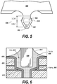
- Figure 5 illustrates the size and dimension of an exemplary compliant pin 502 of an electrical connector 500.
- the compliant pin of the electrical connector discussed herein may be sized and dimensioned to fit into a surface interconnect formed by drilling through one or more layers of a PCB.
- the compliant pin 502 may have a tapered shape created by an inclined side wall provided around the circumference of the compliant pin 502.
- a divot 504 may be provided above the tapered surface of the compliant pin 502.
- the divot 504 may be a continuous divot formed around a circumference of the compliant pin 502.
- the divot 504 may include one or more divots formed above the tapered surface of the compliant pin 502.
- the divot 504 When the electrical connector 500 is coupled and soldered to a PCB 506, the divot 504 may provide a neck to prevent the electrical connector 500 from decoupling from the PCB 506. If the electrical connector 500 is forced to move away from the PCB 506, the divot 504 may hook in the solder 510 provided around the divot 504. The solder 510 above the top surface of the PCB 506 may form a fillet which strengthens the coupling between the compliant pin 502 and the PCB 506.
- the divot 504 of the electrical connector 500 may be up to 0.005" high.
- the height of the soldered divot 504 may be up to 0.006" high.
- a height of the compliant pin 502 of the electrical connector 500 provided beneath the top surface of the PCB 506 may be up to 0.007" high.
- the height of the soldered compliant pin 502 may be up to 0.008" high.
- the solder 508 around the compliant pin 502 may have a tapered surface similar to that of the compliant pin 502.
- the solder 508 around the compliant pin 502 beneath the top surface of the PCB 506 may have a taper angle of up to 27°.
- Figure 6 illustrates a cross section of an exemplary compliant pin coupled to a surface interconnect provided on a surface of a PCB.
- a surface interconnect hole 604 may be drilled on one or more top layers of the PCB 602.
- the surface interconnect hole 604 may be plated using a plating material 606.
- the surface interconnect hole 604 may have a tapered side wall 610 and/or a tapered bottom surface 612.
- the surface interconnect hole 604 may have a diameter of up to 8 millimeters (mm) and a depth of up to 5 millimeters.
- the taper angle of the side wall 610 of the surface interconnect 602 may have at least one of no inclination, a linear inclination up to 15°, and a concave inclination.
- the side wall 610 may a flared entrance aperture.
- a compliant pin 600 may be provided within the surface interconnect hole 604 and soldered therein with solder 608.
- the solder 608 may be provided around the compliant pin 600 within the surface interconnect hole 604 and around the compliant pin 600 above the top surface of the PCB 602.
- the solder above the top surface of the PCB 602 may have a solder fillet 614 with a tapered surface.
- the solder fillet 614 represents a concave surface of the solder at the intersection of electrical connector 600 and top surface of the PCB 602.
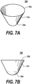
- Figures 7A-7B illustrates the shape, size and dimensions of an exemplary surface interconnect.
- the surface interconnect 700 drilled on and/or into one or more layers of a PCB may have a top surface 702 radius of up to 8 mm, a depth of up to 5 mm and a bottom surface 704 radius equal to or smaller than the top surface 702 radius depending on the inclination of the side wall 710.
- the side wall 710 of the surface interconnect 700 may be tapered to provide a tight fit between the surface interconnect 700 and an electrical connector that may be coupled thereto.
Landscapes
- Engineering & Computer Science (AREA)
- Microelectronics & Electronic Packaging (AREA)
- Manufacturing & Machinery (AREA)
- Coupling Device And Connection With Printed Circuit (AREA)
Claims (12)
- Leiterplatte (482, 492), die Folgendes umfasst:einen mehrschichtigen Körper, der zwischen einer oberen Fläche und einer unteren Fläche angeordnet ist; undmindestens eine verjüngte Oberflächenverbindung (485; 495), die auf der oberen Schicht mechanisch in eine oder mehrere Schichten der Leiterplatte (482, 492) gebohrt ist,wobei die mindestens eine verjüngte Oberflächenverbindung (485, 495) Folgendes aufweist:eine aufgeweitete Eingangsöffnung,eine Bodenfläche (486, 496),eine oder mehrere verjüngte Seitenwände (488) mit einer konkaven Neigung, so dass sich die verjüngte Oberflächenverbindung (481) zur Bodenfläche (486) hin verjüngt, wobei die eine oder die mehreren verjüngten Seitenwände in Bezug auf die verjüngte Oberflächenverbindung (485) zur Leiterplatte hin konkav ist bzw. sind; odereine oder mehrere verjüngte Seitenwände (498), so dass sich die verjüngte Oberflächenverbindung (495) zu der Bodenfläche (496) hin verjüngt und einen gerundeten Schnittpunkt zwischen der Bodenfläche (496) und deren einen oder mehreren verjüngten Seitenwänden (498) aufweist, undund bemessen und konfiguriert ist, um einen verjüngten passenden Stift (481, 491) und Lötmittel aufzunehmen, so dass die verjüngte Oberflächenverbindung (485, 495) dazu geeignet ist, den verjüngten passenden Stift (481, 491) darin zu löten.
- Leiterplatte nach Anspruch 1, wobei die mindestens eine verjüngte Oberflächenverbindung (485, 495) ein plattiertes verjüngtes Loch auf der Leiterplatte (482, 492) ist.
- Leiterplatte nach Anspruch 2, wobei eine Tiefe (212, 262) des plattierten verjüngten Lochs kleiner ist als eine Dicke der Leiterplatte, die durch einen Abstand zwischen der oberen Fläche und der unteren Fläche gebildet ist.
- Elektrische Verbindungsanordnung, die Folgendes umfasst:eine Leiterplatte (482, 492) nach einem der Ansprüche 1 bis 3; undeinen elektrischen Verbinder (484, 494, 500), der mit der mindestens einen verjüngten Oberflächenverbindung (481,491) der Leiterplatte gekoppelt ist, wobei der elektrische Verbinder (484, 494, 500) Folgendes umfasst:einen Verbinderkörper undeinen verjüngten passenden Stift (481, 491), der an einem ersten Ende des Verbinderkörpers angeordnet ist,wobei der verjüngte passende Stift (481,491) Folgendes umfasst:ein verjüngtes Ende (488, 493),wobei der verjüngte passende Stift (481,491) in die mindestens eine Oberflächenverbindung (485, 495) eingesetzt und mit dieser verlötet ist.
- Elektrische Verbindungsanordnung nach Anspruch 4, wobei der verjüngte passende Stift (481, 491) ferner ein Verankerungsmerkmal umfasst, wie einen Verankerungsstift (448) oder einen Korsettanker (468), das mit einem distalen Ende des verjüngten Endes (488, 493) gekoppelt ist.
- Elektrische Verbindungsanordnung nach Anspruch 5, wobei der verjüngte passende Stift (481, 491) ferner eine Vielzahl von Aussparungen (504) über dem verjüngten Ende (488, 493) aufweist.
- Elektrische Verbindungsanordnung nach einem der Ansprüche 4 bis 6, wobei ein Profil des verjüngten Endes des verjüngten passenden Stifts (481,491) mit einem Profil der verjüngten Oberflächenverbindung (485, 495) übereinstimmt.
- Elektrische Verbindungsanordnung nach einem der Ansprüche 4 bis 7, wobei ein Verjüngungswinkel des verjüngten Endes des verjüngten passenden Stifts (481, 491) im Wesentlichen gleich einem Verjüngungswinkel der verjüngten Oberflächenverbindung (485, 495) ist.
- Elektrische Verbindungsanordnung nach einem der Ansprüche 4 bis 8, wobei das verjüngte Ende des verjüngten passenden Stifts (481, 491) in elektrischem Kontakt mit der mindestens einen verjüngten Oberflächenverbindung (485, 495) steht.
- Elektrische Verbindungsanordnung nach einem der Ansprüche 4 bis 9, wobei die mindestens eine verjüngte Oberflächenverbindung (485, 495) ein plattiertes verjüngtes Loch auf der Leiterplatte (482, 492) ist.
- Elektrische Verbindungsanordnung nach Anspruch 10, wobei das verjüngte Ende des verjüngten passenden Stifts (481, 491) nicht in physischem Kontakt mit einer Bodenfläche der mindestens einen verjüngten Oberflächenverbindung (485, 495) steht.
- Elektrische Verbindungsanordnung nach Anspruch 10, wobei eine Tiefe des plattierten verjüngten Lochs kleiner ist als eine Dicke der Leiterplatte, die durch einen Abstand zwischen der oberen Fläche und der unteren Fläche gebildet ist.
Applications Claiming Priority (2)
| Application Number | Priority Date | Filing Date | Title |
|---|---|---|---|
| US14/952,242 US20170149155A1 (en) | 2015-11-25 | 2015-11-25 | Soldered interconnect for a printed circuit board having an angular radial feature |
| PCT/US2016/063260 WO2017091548A1 (en) | 2015-11-25 | 2016-11-22 | Soldered interconnect for a printed circuit board having an angular radial feature |
Publications (2)
| Publication Number | Publication Date |
|---|---|
| EP3381245A1 EP3381245A1 (de) | 2018-10-03 |
| EP3381245B1 true EP3381245B1 (de) | 2021-05-26 |
Family
ID=57544537
Family Applications (1)
| Application Number | Title | Priority Date | Filing Date |
|---|---|---|---|
| EP16810543.5A Active EP3381245B1 (de) | 2015-11-25 | 2016-11-22 | Gelötete verbindung für eine leiterplatte |
Country Status (3)
| Country | Link |
|---|---|
| US (4) | US20170149155A1 (de) |
| EP (1) | EP3381245B1 (de) |
| WO (1) | WO2017091548A1 (de) |
Families Citing this family (10)
| Publication number | Priority date | Publication date | Assignee | Title |
|---|---|---|---|---|
| WO2018232555A1 (en) * | 2017-06-19 | 2018-12-27 | Intel Corporation | A printed circuit board with a connector for electric connection of the pcb with another apparatus |
| CN108260298A (zh) * | 2018-01-11 | 2018-07-06 | 郑州云海信息技术有限公司 | 一种倒梯形结构铜排的焊接方法及铜排 |
| US10517167B1 (en) | 2018-10-19 | 2019-12-24 | Eagle Technology, Llc | Systems and methods for providing a high speed interconnect system with reduced crosstalk |
| US11056850B2 (en) | 2019-07-26 | 2021-07-06 | Eagle Technology, Llc | Systems and methods for providing a soldered interface on a printed circuit board having a blind feature |
| US11602800B2 (en) | 2019-10-10 | 2023-03-14 | Eagle Technology, Llc | Systems and methods for providing an interface on a printed circuit board using pin solder enhancement |
| US11025011B1 (en) * | 2020-02-26 | 2021-06-01 | Genesis Technology Usa, Inc. | RF connector with V-grooved EMI sealing interface |
| US11283204B1 (en) | 2020-11-19 | 2022-03-22 | Eagle Technology, Llc | Systems and methods for providing a composite connector for high speed interconnect systems |
| CN113612054B (zh) * | 2021-08-03 | 2023-05-23 | 深圳市国天电子股份有限公司 | 一种smb连接器及组装装置 |
| US12035482B2 (en) * | 2022-02-07 | 2024-07-09 | Eagle Technology, Llc | Electronic device with multi-diameter female contacts and related methods |
| CN114535884A (zh) * | 2022-04-01 | 2022-05-27 | 四创电子股份有限公司 | 一种smp连接器放焊锡污染工装 |
Family Cites Families (19)
| Publication number | Priority date | Publication date | Assignee | Title |
|---|---|---|---|---|
| US3246386A (en) | 1962-01-26 | 1966-04-19 | Corning Glass Works | Electrical connected component and method |
| US3325752A (en) * | 1965-02-01 | 1967-06-13 | Electronics Standards Corp Of | Microwave connector |
| JPS62229896A (ja) * | 1986-03-29 | 1987-10-08 | 株式会社東芝 | 印刷配線基板 |
| US5516303A (en) * | 1995-01-11 | 1996-05-14 | The Whitaker Corporation | Floating panel-mounted coaxial connector for use with stripline circuit boards |
| TW395603U (en) | 1998-11-10 | 2000-06-21 | Advanced Connectek Inc | Electrical connector |
| EP1150551B1 (de) * | 1998-12-16 | 2007-06-13 | Ibiden Co., Ltd. | Leitender verbindungsstift und baugruppen-platte |
| JP3378550B2 (ja) * | 2000-02-03 | 2003-02-17 | 日本特殊陶業株式会社 | リードピン付き配線基板 |
| US6593535B2 (en) | 2001-06-26 | 2003-07-15 | Teradyne, Inc. | Direct inner layer interconnect for a high speed printed circuit board |
| US7088008B2 (en) * | 2003-03-20 | 2006-08-08 | International Business Machines Corporation | Electronic package with optimized circuitization pattern |
| US7155821B1 (en) * | 2004-06-30 | 2007-01-02 | Emc Corporation | Techniques for manufacturing a circuit board having a countersunk via |
| KR100734264B1 (ko) * | 2005-06-16 | 2007-07-02 | 삼성전자주식회사 | 집적회로 패키지와 집적회로 모듈 |
| JP5006618B2 (ja) * | 2006-10-25 | 2012-08-22 | イリソ電子工業株式会社 | コネクタ |
| US8153900B2 (en) * | 2007-08-30 | 2012-04-10 | Shinko Electric Industries Co., Ltd. | Wiring substrate with lead pin and lead pin |
| WO2009057614A1 (ja) | 2007-10-31 | 2009-05-07 | Nec Corporation | 電子装置及びその製造方法、並びに実装基板 |
| JP4613237B2 (ja) * | 2008-12-10 | 2011-01-12 | 新光電気工業株式会社 | リードピン付配線基板及びリードピン |
| JP5399800B2 (ja) * | 2009-07-17 | 2014-01-29 | 矢崎総業株式会社 | 防水構造 |
| KR101070022B1 (ko) | 2009-09-16 | 2011-10-04 | 삼성전기주식회사 | 다층 세라믹 회로 기판, 다층 세라믹 회로 기판 제조방법 및 이를 이용한 전자 디바이스 모듈 |
| KR101060924B1 (ko) | 2009-09-22 | 2011-08-30 | 삼성전기주식회사 | 패키지 기판용 리드핀 |
| KR101167443B1 (ko) * | 2010-11-17 | 2012-07-19 | 삼성전기주식회사 | 인쇄회로기판용 리드핀과 이를 이용한 인쇄회로기판 |
-
2015
- 2015-11-25 US US14/952,242 patent/US20170149155A1/en not_active Abandoned
-
2016
- 2016-07-01 US US15/200,695 patent/US9761972B2/en active Active
- 2016-11-22 WO PCT/US2016/063260 patent/WO2017091548A1/en not_active Ceased
- 2016-11-22 EP EP16810543.5A patent/EP3381245B1/de active Active
-
2017
- 2017-02-02 US US15/422,978 patent/US20170244184A1/en not_active Abandoned
- 2017-02-02 US US15/423,269 patent/US10096915B2/en active Active
Non-Patent Citations (1)
| Title |
|---|
| None * |
Also Published As
| Publication number | Publication date |
|---|---|
| US10096915B2 (en) | 2018-10-09 |
| WO2017091548A1 (en) | 2017-06-01 |
| US20170149156A1 (en) | 2017-05-25 |
| US9761972B2 (en) | 2017-09-12 |
| US20170149154A1 (en) | 2017-05-25 |
| US20170149155A1 (en) | 2017-05-25 |
| US20170244184A1 (en) | 2017-08-24 |
| EP3381245A1 (de) | 2018-10-03 |
Similar Documents
| Publication | Publication Date | Title |
|---|---|---|
| US10096915B2 (en) | Soldered interconnect for a printed circuit board having an angular radial feature | |
| US6747217B1 (en) | Alternative to through-hole-plating in a printed circuit board | |
| US6593535B2 (en) | Direct inner layer interconnect for a high speed printed circuit board | |
| JP4600910B2 (ja) | 高速相互接続構造 | |
| US4906198A (en) | Circuit board assembly and contact pin for use therein | |
| US20080207015A1 (en) | Press-fit pin and board structure | |
| TWI785211B (zh) | 瞬接式射頻(rf)互連構造 | |
| JP6804888B2 (ja) | 同軸コネクタ | |
| US20130312257A1 (en) | Connecting an electronic component to a printed circuit board | |
| US20110149543A1 (en) | Printed wiring board connection structure | |
| JP2007200728A (ja) | 基板間接続コネクタ | |
| WO2014120319A1 (en) | Connector with staggered contacts | |
| US7400511B2 (en) | Electronic component mounting structure | |
| US9674964B2 (en) | Method and structure for directly connecting coaxial or micro coaxial cables to the interior side of pads of a printed circuit board to improve signal integrity of an electrical circuit | |
| US7918668B1 (en) | Socket connector assembly with conductive posts | |
| US6963494B2 (en) | Blind hole termination of pin to pcb | |
| US10681803B2 (en) | Flexible circuit board with improved bonding flatness | |
| CN110071379A (zh) | 插塞式连接器和电路板的总成 | |
| JP5515849B2 (ja) | プリント基板の結合構造 | |
| US9363916B2 (en) | Connection pin and a method for mounting a connection pin in a component carrier for an electronic assembly, and such a component carrier comprising connection pins | |
| EP3143846B1 (de) | Übertragungsleitungsdurchgangsstruktur | |
| US9451697B2 (en) | High speed printed circuit board with uniform via inside diameter | |
| EP1813001B1 (de) | Mittenebene in zwei stücken | |
| US20250227854A1 (en) | Coverlay as printed circuit board (pcb) voltage insulator under connectors | |
| US9461383B1 (en) | High signal isolation electrical connector |
Legal Events
| Date | Code | Title | Description |
|---|---|---|---|
| STAA | Information on the status of an ep patent application or granted ep patent |
Free format text: STATUS: UNKNOWN |
|
| STAA | Information on the status of an ep patent application or granted ep patent |
Free format text: STATUS: THE INTERNATIONAL PUBLICATION HAS BEEN MADE |
|
| PUAI | Public reference made under article 153(3) epc to a published international application that has entered the european phase |
Free format text: ORIGINAL CODE: 0009012 |
|
| STAA | Information on the status of an ep patent application or granted ep patent |
Free format text: STATUS: REQUEST FOR EXAMINATION WAS MADE |
|
| 17P | Request for examination filed |
Effective date: 20180622 |
|
| AK | Designated contracting states |
Kind code of ref document: A1 Designated state(s): AL AT BE BG CH CY CZ DE DK EE ES FI FR GB GR HR HU IE IS IT LI LT LU LV MC MK MT NL NO PL PT RO RS SE SI SK SM TR |
|
| AX | Request for extension of the european patent |
Extension state: BA ME |
|
| RIN1 | Information on inventor provided before grant (corrected) |
Inventor name: OUELLETTE, ERICA Inventor name: METHRATTA, ABSU Inventor name: MCKENNEY, DARRYL J. |
|
| DAV | Request for validation of the european patent (deleted) | ||
| DAX | Request for extension of the european patent (deleted) | ||
| STAA | Information on the status of an ep patent application or granted ep patent |
Free format text: STATUS: EXAMINATION IS IN PROGRESS |
|
| 17Q | First examination report despatched |
Effective date: 20190402 |
|
| REG | Reference to a national code |
Ref country code: DE Ref legal event code: R079 Ref document number: 602016058515 Country of ref document: DE Free format text: PREVIOUS MAIN CLASS: H05K0001110000 Ipc: H01R0004020000 |
|
| GRAP | Despatch of communication of intention to grant a patent |
Free format text: ORIGINAL CODE: EPIDOSNIGR1 |
|
| STAA | Information on the status of an ep patent application or granted ep patent |
Free format text: STATUS: GRANT OF PATENT IS INTENDED |
|
| RIC1 | Information provided on ipc code assigned before grant |
Ipc: H01R 12/58 20110101ALI20201210BHEP Ipc: H05K 3/30 20060101ALI20201210BHEP Ipc: H05K 3/34 20060101ALI20201210BHEP Ipc: H01R 12/52 20110101ALI20201210BHEP Ipc: H01R 4/02 20060101AFI20201210BHEP Ipc: H05K 3/42 20060101ALN20201210BHEP |
|
| RIC1 | Information provided on ipc code assigned before grant |
Ipc: H01R 12/58 20110101ALI20201211BHEP Ipc: H05K 3/34 20060101ALI20201211BHEP Ipc: H01R 12/52 20110101ALI20201211BHEP Ipc: H05K 3/30 20060101ALI20201211BHEP Ipc: H01R 4/02 20060101AFI20201211BHEP Ipc: H05K 3/42 20060101ALN20201211BHEP |
|
| INTG | Intention to grant announced |
Effective date: 20210113 |
|
| GRAS | Grant fee paid |
Free format text: ORIGINAL CODE: EPIDOSNIGR3 |
|
| GRAA | (expected) grant |
Free format text: ORIGINAL CODE: 0009210 |
|
| STAA | Information on the status of an ep patent application or granted ep patent |
Free format text: STATUS: THE PATENT HAS BEEN GRANTED |
|
| AK | Designated contracting states |
Kind code of ref document: B1 Designated state(s): AL AT BE BG CH CY CZ DE DK EE ES FI FR GB GR HR HU IE IS IT LI LT LU LV MC MK MT NL NO PL PT RO RS SE SI SK SM TR |
|
| REG | Reference to a national code |
Ref country code: GB Ref legal event code: FG4D |
|
| REG | Reference to a national code |
Ref country code: CH Ref legal event code: EP |
|
| REG | Reference to a national code |
Ref country code: AT Ref legal event code: REF Ref document number: 1397170 Country of ref document: AT Kind code of ref document: T Effective date: 20210615 |
|
| REG | Reference to a national code |
Ref country code: DE Ref legal event code: R096 Ref document number: 602016058515 Country of ref document: DE |
|
| REG | Reference to a national code |
Ref country code: IE Ref legal event code: FG4D |
|
| REG | Reference to a national code |
Ref country code: LT Ref legal event code: MG9D |
|
| REG | Reference to a national code |
Ref country code: AT Ref legal event code: MK05 Ref document number: 1397170 Country of ref document: AT Kind code of ref document: T Effective date: 20210526 |
|
| PG25 | Lapsed in a contracting state [announced via postgrant information from national office to epo] |
Ref country code: LT Free format text: LAPSE BECAUSE OF FAILURE TO SUBMIT A TRANSLATION OF THE DESCRIPTION OR TO PAY THE FEE WITHIN THE PRESCRIBED TIME-LIMIT Effective date: 20210526 Ref country code: FI Free format text: LAPSE BECAUSE OF FAILURE TO SUBMIT A TRANSLATION OF THE DESCRIPTION OR TO PAY THE FEE WITHIN THE PRESCRIBED TIME-LIMIT Effective date: 20210526 Ref country code: BG Free format text: LAPSE BECAUSE OF FAILURE TO SUBMIT A TRANSLATION OF THE DESCRIPTION OR TO PAY THE FEE WITHIN THE PRESCRIBED TIME-LIMIT Effective date: 20210826 Ref country code: AT Free format text: LAPSE BECAUSE OF FAILURE TO SUBMIT A TRANSLATION OF THE DESCRIPTION OR TO PAY THE FEE WITHIN THE PRESCRIBED TIME-LIMIT Effective date: 20210526 Ref country code: HR Free format text: LAPSE BECAUSE OF FAILURE TO SUBMIT A TRANSLATION OF THE DESCRIPTION OR TO PAY THE FEE WITHIN THE PRESCRIBED TIME-LIMIT Effective date: 20210526 |
|
| REG | Reference to a national code |
Ref country code: NL Ref legal event code: MP Effective date: 20210526 |
|
| PG25 | Lapsed in a contracting state [announced via postgrant information from national office to epo] |
Ref country code: RS Free format text: LAPSE BECAUSE OF FAILURE TO SUBMIT A TRANSLATION OF THE DESCRIPTION OR TO PAY THE FEE WITHIN THE PRESCRIBED TIME-LIMIT Effective date: 20210526 Ref country code: SE Free format text: LAPSE BECAUSE OF FAILURE TO SUBMIT A TRANSLATION OF THE DESCRIPTION OR TO PAY THE FEE WITHIN THE PRESCRIBED TIME-LIMIT Effective date: 20210526 Ref country code: NO Free format text: LAPSE BECAUSE OF FAILURE TO SUBMIT A TRANSLATION OF THE DESCRIPTION OR TO PAY THE FEE WITHIN THE PRESCRIBED TIME-LIMIT Effective date: 20210826 Ref country code: PT Free format text: LAPSE BECAUSE OF FAILURE TO SUBMIT A TRANSLATION OF THE DESCRIPTION OR TO PAY THE FEE WITHIN THE PRESCRIBED TIME-LIMIT Effective date: 20210927 Ref country code: PL Free format text: LAPSE BECAUSE OF FAILURE TO SUBMIT A TRANSLATION OF THE DESCRIPTION OR TO PAY THE FEE WITHIN THE PRESCRIBED TIME-LIMIT Effective date: 20210526 Ref country code: IS Free format text: LAPSE BECAUSE OF FAILURE TO SUBMIT A TRANSLATION OF THE DESCRIPTION OR TO PAY THE FEE WITHIN THE PRESCRIBED TIME-LIMIT Effective date: 20210926 Ref country code: LV Free format text: LAPSE BECAUSE OF FAILURE TO SUBMIT A TRANSLATION OF THE DESCRIPTION OR TO PAY THE FEE WITHIN THE PRESCRIBED TIME-LIMIT Effective date: 20210526 Ref country code: GR Free format text: LAPSE BECAUSE OF FAILURE TO SUBMIT A TRANSLATION OF THE DESCRIPTION OR TO PAY THE FEE WITHIN THE PRESCRIBED TIME-LIMIT Effective date: 20210827 |
|
| PG25 | Lapsed in a contracting state [announced via postgrant information from national office to epo] |
Ref country code: NL Free format text: LAPSE BECAUSE OF FAILURE TO SUBMIT A TRANSLATION OF THE DESCRIPTION OR TO PAY THE FEE WITHIN THE PRESCRIBED TIME-LIMIT Effective date: 20210526 |
|
| PG25 | Lapsed in a contracting state [announced via postgrant information from national office to epo] |
Ref country code: CZ Free format text: LAPSE BECAUSE OF FAILURE TO SUBMIT A TRANSLATION OF THE DESCRIPTION OR TO PAY THE FEE WITHIN THE PRESCRIBED TIME-LIMIT Effective date: 20210526 Ref country code: EE Free format text: LAPSE BECAUSE OF FAILURE TO SUBMIT A TRANSLATION OF THE DESCRIPTION OR TO PAY THE FEE WITHIN THE PRESCRIBED TIME-LIMIT Effective date: 20210526 Ref country code: DK Free format text: LAPSE BECAUSE OF FAILURE TO SUBMIT A TRANSLATION OF THE DESCRIPTION OR TO PAY THE FEE WITHIN THE PRESCRIBED TIME-LIMIT Effective date: 20210526 Ref country code: ES Free format text: LAPSE BECAUSE OF FAILURE TO SUBMIT A TRANSLATION OF THE DESCRIPTION OR TO PAY THE FEE WITHIN THE PRESCRIBED TIME-LIMIT Effective date: 20210526 Ref country code: RO Free format text: LAPSE BECAUSE OF FAILURE TO SUBMIT A TRANSLATION OF THE DESCRIPTION OR TO PAY THE FEE WITHIN THE PRESCRIBED TIME-LIMIT Effective date: 20210526 Ref country code: SK Free format text: LAPSE BECAUSE OF FAILURE TO SUBMIT A TRANSLATION OF THE DESCRIPTION OR TO PAY THE FEE WITHIN THE PRESCRIBED TIME-LIMIT Effective date: 20210526 Ref country code: SM Free format text: LAPSE BECAUSE OF FAILURE TO SUBMIT A TRANSLATION OF THE DESCRIPTION OR TO PAY THE FEE WITHIN THE PRESCRIBED TIME-LIMIT Effective date: 20210526 |
|
| REG | Reference to a national code |
Ref country code: DE Ref legal event code: R097 Ref document number: 602016058515 Country of ref document: DE |
|
| PLBE | No opposition filed within time limit |
Free format text: ORIGINAL CODE: 0009261 |
|
| STAA | Information on the status of an ep patent application or granted ep patent |
Free format text: STATUS: NO OPPOSITION FILED WITHIN TIME LIMIT |
|
| 26N | No opposition filed |
Effective date: 20220301 |
|
| PG25 | Lapsed in a contracting state [announced via postgrant information from national office to epo] |
Ref country code: IS Free format text: LAPSE BECAUSE OF FAILURE TO SUBMIT A TRANSLATION OF THE DESCRIPTION OR TO PAY THE FEE WITHIN THE PRESCRIBED TIME-LIMIT Effective date: 20210926 Ref country code: AL Free format text: LAPSE BECAUSE OF FAILURE TO SUBMIT A TRANSLATION OF THE DESCRIPTION OR TO PAY THE FEE WITHIN THE PRESCRIBED TIME-LIMIT Effective date: 20210526 |
|
| PG25 | Lapsed in a contracting state [announced via postgrant information from national office to epo] |
Ref country code: MC Free format text: LAPSE BECAUSE OF FAILURE TO SUBMIT A TRANSLATION OF THE DESCRIPTION OR TO PAY THE FEE WITHIN THE PRESCRIBED TIME-LIMIT Effective date: 20210526 |
|
| REG | Reference to a national code |
Ref country code: CH Ref legal event code: PL |
|
| PG25 | Lapsed in a contracting state [announced via postgrant information from national office to epo] |
Ref country code: LU Free format text: LAPSE BECAUSE OF NON-PAYMENT OF DUE FEES Effective date: 20211122 Ref country code: IT Free format text: LAPSE BECAUSE OF FAILURE TO SUBMIT A TRANSLATION OF THE DESCRIPTION OR TO PAY THE FEE WITHIN THE PRESCRIBED TIME-LIMIT Effective date: 20210526 Ref country code: BE Free format text: LAPSE BECAUSE OF NON-PAYMENT OF DUE FEES Effective date: 20211130 |
|
| REG | Reference to a national code |
Ref country code: BE Ref legal event code: MM Effective date: 20211130 |
|
| PG25 | Lapsed in a contracting state [announced via postgrant information from national office to epo] |
Ref country code: LI Free format text: LAPSE BECAUSE OF NON-PAYMENT OF DUE FEES Effective date: 20211130 Ref country code: CH Free format text: LAPSE BECAUSE OF NON-PAYMENT OF DUE FEES Effective date: 20211130 |
|
| PG25 | Lapsed in a contracting state [announced via postgrant information from national office to epo] |
Ref country code: IE Free format text: LAPSE BECAUSE OF NON-PAYMENT OF DUE FEES Effective date: 20211122 |
|
| PG25 | Lapsed in a contracting state [announced via postgrant information from national office to epo] |
Ref country code: HU Free format text: LAPSE BECAUSE OF FAILURE TO SUBMIT A TRANSLATION OF THE DESCRIPTION OR TO PAY THE FEE WITHIN THE PRESCRIBED TIME-LIMIT; INVALID AB INITIO Effective date: 20161122 |
|
| P01 | Opt-out of the competence of the unified patent court (upc) registered |
Effective date: 20230508 |
|
| PG25 | Lapsed in a contracting state [announced via postgrant information from national office to epo] |
Ref country code: CY Free format text: LAPSE BECAUSE OF FAILURE TO SUBMIT A TRANSLATION OF THE DESCRIPTION OR TO PAY THE FEE WITHIN THE PRESCRIBED TIME-LIMIT Effective date: 20210526 |
|
| PG25 | Lapsed in a contracting state [announced via postgrant information from national office to epo] |
Ref country code: MK Free format text: LAPSE BECAUSE OF FAILURE TO SUBMIT A TRANSLATION OF THE DESCRIPTION OR TO PAY THE FEE WITHIN THE PRESCRIBED TIME-LIMIT Effective date: 20210526 |
|
| PG25 | Lapsed in a contracting state [announced via postgrant information from national office to epo] |
Ref country code: TR Free format text: LAPSE BECAUSE OF FAILURE TO SUBMIT A TRANSLATION OF THE DESCRIPTION OR TO PAY THE FEE WITHIN THE PRESCRIBED TIME-LIMIT Effective date: 20210526 |
|
| PG25 | Lapsed in a contracting state [announced via postgrant information from national office to epo] |
Ref country code: MT Free format text: LAPSE BECAUSE OF FAILURE TO SUBMIT A TRANSLATION OF THE DESCRIPTION OR TO PAY THE FEE WITHIN THE PRESCRIBED TIME-LIMIT Effective date: 20210526 |
|
| PGFP | Annual fee paid to national office [announced via postgrant information from national office to epo] |
Ref country code: DE Payment date: 20251119 Year of fee payment: 10 |
|
| PGFP | Annual fee paid to national office [announced via postgrant information from national office to epo] |
Ref country code: GB Payment date: 20251121 Year of fee payment: 10 |
|
| PGFP | Annual fee paid to national office [announced via postgrant information from national office to epo] |
Ref country code: FR Payment date: 20251126 Year of fee payment: 10 |