EP3379578A1 - Semiconductor device - Google Patents

Semiconductor device Download PDF

Info

Publication number
EP3379578A1
EP3379578A1 EP18153174.0A EP18153174A EP3379578A1 EP 3379578 A1 EP3379578 A1 EP 3379578A1 EP 18153174 A EP18153174 A EP 18153174A EP 3379578 A1 EP3379578 A1 EP 3379578A1
Authority
EP
European Patent Office
Prior art keywords
layer
semiconductor device
gate electrode
semiconductor layer
angle
Prior art date
Legal status (The legal status is an assumption and is not a legal conclusion. Google has not performed a legal analysis and makes no representation as to the accuracy of the status listed.)
Withdrawn
Application number
EP18153174.0A
Other languages
German (de)
French (fr)
Inventor
Keiichi Matsushita
Current Assignee (The listed assignees may be inaccurate. Google has not performed a legal analysis and makes no representation or warranty as to the accuracy of the list.)
Toshiba Corp
Toshiba Infrastructure Systems and Solutions Corp
Original Assignee
Toshiba Corp
Toshiba Infrastructure Systems and Solutions Corp
Priority date (The priority date is an assumption and is not a legal conclusion. Google has not performed a legal analysis and makes no representation as to the accuracy of the date listed.)
Filing date
Publication date
Application filed by Toshiba Corp, Toshiba Infrastructure Systems and Solutions Corp filed Critical Toshiba Corp
Publication of EP3379578A1 publication Critical patent/EP3379578A1/en
Withdrawn legal-status Critical Current

Links

Images

Classifications

    • HELECTRICITY
    • H10SEMICONDUCTOR DEVICES; ELECTRIC SOLID-STATE DEVICES NOT OTHERWISE PROVIDED FOR
    • H10DINORGANIC ELECTRIC SEMICONDUCTOR DEVICES
    • H10D30/00Field-effect transistors [FET]
    • H10D30/01Manufacture or treatment
    • H10D30/015Manufacture or treatment of FETs having heterojunction interface channels or heterojunction gate electrodes, e.g. HEMT
    • HELECTRICITY
    • H10SEMICONDUCTOR DEVICES; ELECTRIC SOLID-STATE DEVICES NOT OTHERWISE PROVIDED FOR
    • H10DINORGANIC ELECTRIC SEMICONDUCTOR DEVICES
    • H10D30/00Field-effect transistors [FET]
    • H10D30/40FETs having zero-dimensional [0D], one-dimensional [1D] or two-dimensional [2D] charge carrier gas channels
    • H10D30/47FETs having zero-dimensional [0D], one-dimensional [1D] or two-dimensional [2D] charge carrier gas channels having two-dimensional [2D] charge carrier gas channels, e.g. nanoribbon FETs or high electron mobility transistors [HEMT]
    • H10D30/471High electron mobility transistors [HEMT] or high hole mobility transistors [HHMT]
    • H10D30/475High electron mobility transistors [HEMT] or high hole mobility transistors [HHMT] having wider bandgap layer formed on top of lower bandgap active layer, e.g. undoped barrier HEMTs such as i-AlGaN/GaN HEMTs
    • HELECTRICITY
    • H10SEMICONDUCTOR DEVICES; ELECTRIC SOLID-STATE DEVICES NOT OTHERWISE PROVIDED FOR
    • H10DINORGANIC ELECTRIC SEMICONDUCTOR DEVICES
    • H10D30/00Field-effect transistors [FET]
    • H10D30/40FETs having zero-dimensional [0D], one-dimensional [1D] or two-dimensional [2D] charge carrier gas channels
    • H10D30/47FETs having zero-dimensional [0D], one-dimensional [1D] or two-dimensional [2D] charge carrier gas channels having two-dimensional [2D] charge carrier gas channels, e.g. nanoribbon FETs or high electron mobility transistors [HEMT]
    • H10D30/471High electron mobility transistors [HEMT] or high hole mobility transistors [HHMT]
    • H10D30/475High electron mobility transistors [HEMT] or high hole mobility transistors [HHMT] having wider bandgap layer formed on top of lower bandgap active layer, e.g. undoped barrier HEMTs such as i-AlGaN/GaN HEMTs
    • H10D30/4755High electron mobility transistors [HEMT] or high hole mobility transistors [HHMT] having wider bandgap layer formed on top of lower bandgap active layer, e.g. undoped barrier HEMTs such as i-AlGaN/GaN HEMTs having wide bandgap charge-carrier supplying layers, e.g. modulation doped HEMTs such as n-AlGaAs/GaAs HEMTs
    • HELECTRICITY
    • H10SEMICONDUCTOR DEVICES; ELECTRIC SOLID-STATE DEVICES NOT OTHERWISE PROVIDED FOR
    • H10DINORGANIC ELECTRIC SEMICONDUCTOR DEVICES
    • H10D62/00Semiconductor bodies, or regions thereof, of devices having potential barriers
    • H10D62/80Semiconductor bodies, or regions thereof, of devices having potential barriers characterised by the materials
    • H10D62/82Heterojunctions
    • H10D62/824Heterojunctions comprising only Group III-V materials heterojunctions, e.g. GaN/AlGaN heterojunctions
    • HELECTRICITY
    • H10SEMICONDUCTOR DEVICES; ELECTRIC SOLID-STATE DEVICES NOT OTHERWISE PROVIDED FOR
    • H10DINORGANIC ELECTRIC SEMICONDUCTOR DEVICES
    • H10D62/00Semiconductor bodies, or regions thereof, of devices having potential barriers
    • H10D62/80Semiconductor bodies, or regions thereof, of devices having potential barriers characterised by the materials
    • H10D62/85Semiconductor bodies, or regions thereof, of devices having potential barriers characterised by the materials being Group III-V materials, e.g. GaAs
    • H10D62/8503Nitride Group III-V materials, e.g. AlN or GaN
    • HELECTRICITY
    • H10SEMICONDUCTOR DEVICES; ELECTRIC SOLID-STATE DEVICES NOT OTHERWISE PROVIDED FOR
    • H10DINORGANIC ELECTRIC SEMICONDUCTOR DEVICES
    • H10D64/00Electrodes of devices having potential barriers
    • H10D64/01Manufacture or treatment
    • H10D64/013Manufacture or treatment of electrodes having a conductor capacitively coupled to a semiconductor by an insulator
    • H10D64/01358Manufacture or treatment of electrodes having a conductor capacitively coupled to a semiconductor by an insulator the insulator being formed after the semiconductor body, the semiconductor being a Group III-V material
    • HELECTRICITY
    • H10SEMICONDUCTOR DEVICES; ELECTRIC SOLID-STATE DEVICES NOT OTHERWISE PROVIDED FOR
    • H10DINORGANIC ELECTRIC SEMICONDUCTOR DEVICES
    • H10D64/00Electrodes of devices having potential barriers
    • H10D64/20Electrodes characterised by their shapes, relative sizes or dispositions 
    • H10D64/23Electrodes carrying the current to be rectified, amplified, oscillated or switched, e.g. sources, drains, anodes or cathodes
    • H10D64/251Source or drain electrodes for field-effect devices
    • H10D64/258Source or drain electrodes for field-effect devices characterised by the relative positions of the source or drain electrodes with respect to the gate electrode
    • HELECTRICITY
    • H10SEMICONDUCTOR DEVICES; ELECTRIC SOLID-STATE DEVICES NOT OTHERWISE PROVIDED FOR
    • H10DINORGANIC ELECTRIC SEMICONDUCTOR DEVICES
    • H10D64/00Electrodes of devices having potential barriers
    • H10D64/20Electrodes characterised by their shapes, relative sizes or dispositions 
    • H10D64/27Electrodes not carrying the current to be rectified, amplified, oscillated or switched, e.g. gates
    • H10D64/311Gate electrodes for field-effect devices
    • H10D64/411Gate electrodes for field-effect devices for FETs
    • HELECTRICITY
    • H10SEMICONDUCTOR DEVICES; ELECTRIC SOLID-STATE DEVICES NOT OTHERWISE PROVIDED FOR
    • H10DINORGANIC ELECTRIC SEMICONDUCTOR DEVICES
    • H10D64/00Electrodes of devices having potential barriers
    • H10D64/20Electrodes characterised by their shapes, relative sizes or dispositions 
    • H10D64/27Electrodes not carrying the current to be rectified, amplified, oscillated or switched, e.g. gates
    • H10D64/311Gate electrodes for field-effect devices
    • H10D64/411Gate electrodes for field-effect devices for FETs
    • H10D64/511Gate electrodes for field-effect devices for FETs for IGFETs
    • H10D64/514Gate electrodes for field-effect devices for FETs for IGFETs characterised by the insulating layers
    • H10D64/516Gate electrodes for field-effect devices for FETs for IGFETs characterised by the insulating layers the thicknesses being non-uniform
    • HELECTRICITY
    • H10SEMICONDUCTOR DEVICES; ELECTRIC SOLID-STATE DEVICES NOT OTHERWISE PROVIDED FOR
    • H10DINORGANIC ELECTRIC SEMICONDUCTOR DEVICES
    • H10D64/00Electrodes of devices having potential barriers
    • H10D64/20Electrodes characterised by their shapes, relative sizes or dispositions 
    • H10D64/27Electrodes not carrying the current to be rectified, amplified, oscillated or switched, e.g. gates
    • H10D64/311Gate electrodes for field-effect devices
    • H10D64/411Gate electrodes for field-effect devices for FETs
    • H10D64/511Gate electrodes for field-effect devices for FETs for IGFETs
    • H10D64/517Gate electrodes for field-effect devices for FETs for IGFETs characterised by the conducting layers
    • H10D64/518Gate electrodes for field-effect devices for FETs for IGFETs characterised by the conducting layers characterised by their lengths or sectional shapes
    • HELECTRICITY
    • H10SEMICONDUCTOR DEVICES; ELECTRIC SOLID-STATE DEVICES NOT OTHERWISE PROVIDED FOR
    • H10DINORGANIC ELECTRIC SEMICONDUCTOR DEVICES
    • H10D64/00Electrodes of devices having potential barriers
    • H10D64/20Electrodes characterised by their shapes, relative sizes or dispositions 
    • H10D64/27Electrodes not carrying the current to be rectified, amplified, oscillated or switched, e.g. gates
    • H10D64/311Gate electrodes for field-effect devices
    • H10D64/411Gate electrodes for field-effect devices for FETs
    • H10D64/511Gate electrodes for field-effect devices for FETs for IGFETs
    • H10D64/517Gate electrodes for field-effect devices for FETs for IGFETs characterised by the conducting layers
    • H10D64/519Gate electrodes for field-effect devices for FETs for IGFETs characterised by the conducting layers characterised by their top-view geometrical layouts
    • HELECTRICITY
    • H10SEMICONDUCTOR DEVICES; ELECTRIC SOLID-STATE DEVICES NOT OTHERWISE PROVIDED FOR
    • H10DINORGANIC ELECTRIC SEMICONDUCTOR DEVICES
    • H10D64/00Electrodes of devices having potential barriers
    • H10D64/60Electrodes characterised by their materials
    • H10D64/66Electrodes having a conductor capacitively coupled to a semiconductor by an insulator, e.g. MIS electrodes
    • H10D64/671Electrodes having a conductor capacitively coupled to a semiconductor by an insulator, e.g. MIS electrodes the conductor having lateral variation in doping or structure
    • HELECTRICITY
    • H10SEMICONDUCTOR DEVICES; ELECTRIC SOLID-STATE DEVICES NOT OTHERWISE PROVIDED FOR
    • H10DINORGANIC ELECTRIC SEMICONDUCTOR DEVICES
    • H10D64/00Electrodes of devices having potential barriers
    • H10D64/60Electrodes characterised by their materials
    • H10D64/66Electrodes having a conductor capacitively coupled to a semiconductor by an insulator, e.g. MIS electrodes
    • H10D64/68Electrodes having a conductor capacitively coupled to a semiconductor by an insulator, e.g. MIS electrodes characterised by the insulator, e.g. by the gate insulator
    • H10D64/693Electrodes having a conductor capacitively coupled to a semiconductor by an insulator, e.g. MIS electrodes characterised by the insulator, e.g. by the gate insulator the insulator comprising nitrogen, e.g. nitrides, oxynitrides or nitrogen-doped materials
    • HELECTRICITY
    • H10SEMICONDUCTOR DEVICES; ELECTRIC SOLID-STATE DEVICES NOT OTHERWISE PROVIDED FOR
    • H10PGENERIC PROCESSES OR APPARATUS FOR THE MANUFACTURE OR TREATMENT OF DEVICES COVERED BY CLASS H10
    • H10P14/00Formation of materials, e.g. in the shape of layers or pillars
    • H10P14/60Formation of materials, e.g. in the shape of layers or pillars of insulating materials
    • H10P14/63Formation of materials, e.g. in the shape of layers or pillars of insulating materials characterised by the formation processes
    • H10P14/6326Deposition processes
    • H10P14/6328Deposition from the gas or vapour phase
    • H10P14/6334Deposition from the gas or vapour phase using decomposition or reaction of gaseous or vapour phase compounds, i.e. chemical vapour deposition
    • H10P14/6336Deposition from the gas or vapour phase using decomposition or reaction of gaseous or vapour phase compounds, i.e. chemical vapour deposition in the presence of a plasma [PECVD]
    • HELECTRICITY
    • H10SEMICONDUCTOR DEVICES; ELECTRIC SOLID-STATE DEVICES NOT OTHERWISE PROVIDED FOR
    • H10PGENERIC PROCESSES OR APPARATUS FOR THE MANUFACTURE OR TREATMENT OF DEVICES COVERED BY CLASS H10
    • H10P14/00Formation of materials, e.g. in the shape of layers or pillars
    • H10P14/60Formation of materials, e.g. in the shape of layers or pillars of insulating materials
    • H10P14/66Formation of materials, e.g. in the shape of layers or pillars of insulating materials characterised by the type of materials
    • H10P14/668Formation of materials, e.g. in the shape of layers or pillars of insulating materials characterised by the type of materials the materials being characterised by the deposition precursor materials
    • H10P14/6681Formation of materials, e.g. in the shape of layers or pillars of insulating materials characterised by the type of materials the materials being characterised by the deposition precursor materials the precursor containing a compound comprising Si
    • H10P14/6682Formation of materials, e.g. in the shape of layers or pillars of insulating materials characterised by the type of materials the materials being characterised by the deposition precursor materials the precursor containing a compound comprising Si the compound being a silane, e.g. disilane, methylsilane or chlorosilane
    • HELECTRICITY
    • H10SEMICONDUCTOR DEVICES; ELECTRIC SOLID-STATE DEVICES NOT OTHERWISE PROVIDED FOR
    • H10PGENERIC PROCESSES OR APPARATUS FOR THE MANUFACTURE OR TREATMENT OF DEVICES COVERED BY CLASS H10
    • H10P14/00Formation of materials, e.g. in the shape of layers or pillars
    • H10P14/60Formation of materials, e.g. in the shape of layers or pillars of insulating materials
    • H10P14/69Inorganic materials
    • H10P14/694Inorganic materials composed of nitrides
    • H10P14/6943Inorganic materials composed of nitrides containing silicon
    • H10P14/69433Inorganic materials composed of nitrides containing silicon the material being a silicon nitride not containing oxygen, e.g. SixNy or SixByNz
    • HELECTRICITY
    • H10SEMICONDUCTOR DEVICES; ELECTRIC SOLID-STATE DEVICES NOT OTHERWISE PROVIDED FOR
    • H10PGENERIC PROCESSES OR APPARATUS FOR THE MANUFACTURE OR TREATMENT OF DEVICES COVERED BY CLASS H10
    • H10P50/00Etching of wafers, substrates or parts of devices
    • H10P50/20Dry etching; Plasma etching; Reactive-ion etching
    • H10P50/28Dry etching; Plasma etching; Reactive-ion etching of insulating materials
    • H10P50/282Dry etching; Plasma etching; Reactive-ion etching of insulating materials of inorganic materials
    • H10P50/283Dry etching; Plasma etching; Reactive-ion etching of insulating materials of inorganic materials by chemical means
    • HELECTRICITY
    • H10SEMICONDUCTOR DEVICES; ELECTRIC SOLID-STATE DEVICES NOT OTHERWISE PROVIDED FOR
    • H10PGENERIC PROCESSES OR APPARATUS FOR THE MANUFACTURE OR TREATMENT OF DEVICES COVERED BY CLASS H10
    • H10P50/00Etching of wafers, substrates or parts of devices
    • H10P50/73Etching of wafers, substrates or parts of devices using masks for insulating materials
    • HELECTRICITY
    • H10SEMICONDUCTOR DEVICES; ELECTRIC SOLID-STATE DEVICES NOT OTHERWISE PROVIDED FOR
    • H10WGENERIC PACKAGES, INTERCONNECTIONS, CONNECTORS OR OTHER CONSTRUCTIONAL DETAILS OF DEVICES COVERED BY CLASS H10
    • H10W74/00Encapsulations, e.g. protective coatings
    • H10W74/40Encapsulations, e.g. protective coatings characterised by their materials
    • H10W74/43Encapsulations, e.g. protective coatings characterised by their materials comprising oxides, nitrides or carbides, e.g. ceramics or glasses
    • HELECTRICITY
    • H10SEMICONDUCTOR DEVICES; ELECTRIC SOLID-STATE DEVICES NOT OTHERWISE PROVIDED FOR
    • H10PGENERIC PROCESSES OR APPARATUS FOR THE MANUFACTURE OR TREATMENT OF DEVICES COVERED BY CLASS H10
    • H10P14/00Formation of materials, e.g. in the shape of layers or pillars
    • H10P14/20Formation of materials, e.g. in the shape of layers or pillars of semiconductor materials
    • H10P14/24Formation of materials, e.g. in the shape of layers or pillars of semiconductor materials using chemical vapour deposition [CVD]
    • HELECTRICITY
    • H10SEMICONDUCTOR DEVICES; ELECTRIC SOLID-STATE DEVICES NOT OTHERWISE PROVIDED FOR
    • H10PGENERIC PROCESSES OR APPARATUS FOR THE MANUFACTURE OR TREATMENT OF DEVICES COVERED BY CLASS H10
    • H10P14/00Formation of materials, e.g. in the shape of layers or pillars
    • H10P14/20Formation of materials, e.g. in the shape of layers or pillars of semiconductor materials
    • H10P14/29Formation of materials, e.g. in the shape of layers or pillars of semiconductor materials characterised by the substrates
    • H10P14/2901Materials
    • H10P14/2902Materials being Group IVA materials
    • H10P14/2904Silicon carbide
    • HELECTRICITY
    • H10SEMICONDUCTOR DEVICES; ELECTRIC SOLID-STATE DEVICES NOT OTHERWISE PROVIDED FOR
    • H10PGENERIC PROCESSES OR APPARATUS FOR THE MANUFACTURE OR TREATMENT OF DEVICES COVERED BY CLASS H10
    • H10P14/00Formation of materials, e.g. in the shape of layers or pillars
    • H10P14/20Formation of materials, e.g. in the shape of layers or pillars of semiconductor materials
    • H10P14/34Deposited materials, e.g. layers
    • H10P14/3402Deposited materials, e.g. layers characterised by the chemical composition
    • H10P14/3414Deposited materials, e.g. layers characterised by the chemical composition being group IIIA-VIA materials
    • H10P14/3416Nitrides

Definitions

  • Embodiments described herein relate generally to a semiconductor device.
  • a gallium nitride semiconductor device As a semiconductor device employed in a communication apparatus or the like (such as a high-electron-mobility transistor (HEMT)), a gallium nitride semiconductor device is known in the art.
  • the gallium nitride semiconductor device has a semiconductor layer, various electrodes such as a gate electrode provided on the semiconductor layer, and an insulation layer.
  • the gallium nitride semiconductor device has a higher dielectric strength than that of a silicon-based semiconductor device or a GaAs-based semiconductor device. For this reason, it is possible to increase an output power density by boosting an operating voltage of the semiconductor device.
  • the GaN layer 11 and the AlGaN layer 12 have different bandgap energies. If semiconductor layers having different bandgap energies are bonded, electrons of the semiconductor layer serving as an electron supply layer and having lower electron affinity are collected in the semiconductor layer serving as the electron transport layer and having higher electron affinity. As a result, electrons are accumulated in the vicinity of the bonding surface (heterojunction interface) of the electron transport layer side so as to form a two-dimensional electron gas.
  • the gate electrode 20 and the drain electrode 30 are spaced from each other, and the gate electrode 20 and the source electrode 40 are spaced from each other.
  • the second insulation layer 52 is exposed from the opening formed in the third insulation layer 53 through the etching.
  • the exposed second insulation layer 52 is also etched further.
  • the opening of the third insulation layer 53 is enlarged, and the exposed surface of the second insulation layer 52 is widened, so that etching is performed further.

Landscapes

  • Junction Field-Effect Transistors (AREA)
  • Electrodes Of Semiconductors (AREA)
  • Chemical & Material Sciences (AREA)
  • Chemical Kinetics & Catalysis (AREA)
  • General Chemical & Material Sciences (AREA)
  • Physics & Mathematics (AREA)
  • Engineering & Computer Science (AREA)
  • Plasma & Fusion (AREA)

Abstract

A semiconductor device (1,2) includes a semiconductor layer (13) provided on a substrate (10), a drain electrode (30) and a source electrode (40) provided on the semiconductor layer, and a gate electrode (20) provided on the semiconductor layer such that an angle between a lateral surface and the semiconductor layer gradually decreases toward the semiconductor layer.

Description

    FIELD
  • Embodiments described herein relate generally to a semiconductor device.
  • BACKGROUND
  • As a semiconductor device employed in a communication apparatus or the like (such as a high-electron-mobility transistor (HEMT)), a gallium nitride semiconductor device is known in the art. The gallium nitride semiconductor device has a semiconductor layer, various electrodes such as a gate electrode provided on the semiconductor layer, and an insulation layer. The gallium nitride semiconductor device has a higher dielectric strength than that of a silicon-based semiconductor device or a GaAs-based semiconductor device. For this reason, it is possible to increase an output power density by boosting an operating voltage of the semiconductor device.
  • When the operating voltage of the semiconductor device is boosted, an electric field intensity increases in the vicinity of an edge formed in a boundary between a bottom surface and a lateral surface of a gate electrode bonded to the semiconductor layer, so that a dielectric breakdown is generated between the gate electrode and the semiconductor layer in some cases. In this regard, a new sloped surface is provided between the lateral surface and the bottom surface of the gate electrode by chamfering the edge of the gate electrode. As a result, an angle of the edge formed by the bottom surface and the sloped surface of the gate electrode becomes larger than 90°, so that the electric field intensity in the vicinity of the edge is lowered. As a result, the dielectric breakdown generated between the gate electrode and the semiconductor layer is suppressed. Therefore, it is possible to increase a service life of the semiconductor device.
  • In order to suppress an electric field concentration in the vicinity of the edge formed by the bottom surface and the sloped surface of the electrode, it is necessary to reduce the angle between the sloped surface and the semiconductor layer at a certain level. Meanwhile, when the sloped surface is provided, an effective gate length of the gate electrode increases, so that a high-frequency characteristic of the semiconductor device is degraded.
  • BRIEF DESCRIPTION OF THE DRAWINGS
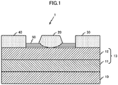
    • FIG. 1 is a cross-sectional view illustrating a semiconductor device according to an embodiment of the invention;
    • FIG. 2 is a diagram illustrating the vicinity of a drain-side lateral surface of the gate electrode of FIG. 1;
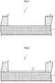
    • FIG. 3 is a diagram illustrating a process of forming a surface protection layer on an AlGaN layer;
    • FIG. 4 is a diagram illustrating a process of forming a surface protection layer on an AlGaN layer;
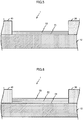
    • FIG. 5 is a diagram illustrating a process of forming a surface protection layer on an AlGaN layer;
    • FIG. 6 is a diagram illustrating a process of forming a surface protection layer on an AlGaN layer;
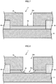
    • FIG. 7 is a diagram illustrating a process of forming an opening in the surface protection layer;
    • FIG. 8 is a diagram illustrating a process of forming an opening in the surface protection layer;
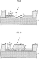
    • FIG. 9 is a diagram illustrating a process of forming an opening in the surface protection layer;
    • FIG. 10 is a diagram illustrating a gate electrode according to an embodiment of the invention; and
    • FIG. 11 is a cross-sectional view illustrating a semiconductor device according to a modification of the embodiment of the invention.
    DETAILED DESCRIPTION
  • An exemplary semiconductor device according to an embodiment of the invention will now be described in details with reference to the accompanying drawings.
  • FIG. 1 is a cross-sectional view illustrating a semiconductor device 1 according to an embodiment of the invention. The semiconductor device 1 according to this embodiment includes a substrate 10, a compound semiconductor layer 13, a gate electrode 20, a drain electrode 30, a source electrode 40, and a surface protection layer 50.
  • The substrate 10 is, for example, a semi-insulating SiC substrate. The compound semiconductor layer 13 is formed on a top surface of the substrate 10 and includes a GaN layer 11 and an AlGaN layer 12.
  • The GaN layer 11 is an electron transport layer formed on the top surface of the substrate 10 using a gas mixture of a trimethyl gallium gas and an ammonia gas, for example, on the basis of a metal organic chemical vapor deposition (MOCVD) method.
  • The AlGaN layer 12 is an electron supply layer formed on the top surface of the GaN layer 11 by using a gas mixture of a trimethyl aluminum gas, a trimethyl gallium gas, and an ammonia gas as a source gas, for example, on the basis of the MOCVD method.
  • The GaN layer 11 and the AlGaN layer 12 have different bandgap energies. If semiconductor layers having different bandgap energies are bonded, electrons of the semiconductor layer serving as an electron supply layer and having lower electron affinity are collected in the semiconductor layer serving as the electron transport layer and having higher electron affinity. As a result, electrons are accumulated in the vicinity of the bonding surface (heterojunction interface) of the electron transport layer side so as to form a two-dimensional electron gas.
  • The two-dimensional electron gas has a state in which electrons are distributed in a planar shape of the semiconductor. Since the electrons distributed in a planar shape do not easily move in a vertical direction, a movement direction of the electrons is limited to a horizontal direction. For this reason, the electrons of the two-dimensional electron gas have high mobility.
  • The GaN layer 11 has electron affinity higher than that of the AlGaN layer 12. For this reason, the GaN layer 11 serves as an electron transport layer side.
  • As illustrated in FIG. 1, the gate electrode 20, the drain electrode 30, and the source electrode 40 are provided on the top surface of the AlGaN layer 12.
  • The gate electrode 20 is provided in the center of the AlGaN layer 12. The gate electrode 20 makes Schottky contact (bonding) with the AlGaN layer 12. In the Schottky contact, a resistance is different between when electrons flow from the gate electrode 20 to the AlGaN layer 12 and when electrons flow from the AlGaN layer 12 to the gate electrode 20. A shape of the gate electrode 20 or a method of forming the gate electrode 20 will be described below.
  • The drain electrode 30 is provided in one of the outer ends of the top surface of the AlGaN layer 12. The drain electrode 30 is formed by depositing, for example, titanium and aluminum on the AlGaN layer 12.
  • The source electrode 40 is provided in the outer end of the top surface of the AlGaN layer 12 by interposing the gate electrode 20 between the source electrode 40 and the drain electrode 30. The source electrode 40 is formed by depositing, for example, titanium and aluminum on the AlGaN layer 12. The source electrode 40 makes ohmic contact with the AlGaN layer 12.
  • The gate electrode 20 and the drain electrode 30 are spaced from each other, and the gate electrode 20 and the source electrode 40 are spaced from each other.
  • During operation of the semiconductor device 1, electrons move from the source electrode 40 to the drain electrode 30 through the two-dimensional electron gas layer formed under the AlGaN layer.
  • The surface protection layer 50 which is an SiN layer serving as an insulation layer is formed on the top surface of the AlGaN layer 12 exposed between the source electrode 40 and the gate electrode 20 and between the gate electrode 20 and the drain electrode 30. The surface protection layer 50 terminates a dangling bond to protect a surface of the AlGaN layer 12 from moisture or the like.
  • FIG. 2 is a diagram illustrating the vicinity of the lateral surface of the gate electrode 20. As illustrated in FIG. 2, the surface protection layer 50 includes a first insulation layer 51, a second insulation layer 52, and a third insulation layer 53 having different etching rates.
  • The first insulation layer 51 is a SiN layer formed on the top surface of the AlGaN layer 12 with a predetermined etching rate.
  • The second insulation layer 52 is a SiN layer formed on the top surface of the first insulation layer 51 with an etching rate higher than that of the first insulation layer 51.
  • The third insulation layer 53 is a SiN layer formed on the top surface of the second insulation layer 52 with an etching rate higher than that of the second insulation layer 52.
  • The gate electrode 20 includes a head portion 21 formed in an upper half of the gate electrode 20, and a stem portion 22 formed in a lower half of the gate electrode 20. The head portion 21 has a substantially trapezoidal cross-sectional shape.
  • The stem portion 22 has a first slope portion 22a, a second slope portion 22b, and a third slope portion 22c.
  • The first slope portion 22a is provided in a lower end of the stem portion 22 and joins with the AlGaN layer 12.
  • Both lateral surfaces of the first slope portion 22a are sloped surfaces respectively inclined to the AlGaN layer 12. The first slope portion 22a is tapered such that its diameter is narrowed toward the lower end of the stem portion 22. An angle θ1 between the sloped surface of the first slope portion 22a and a surface parallel to the top surface of the AlGaN layer 12 is smaller than 90°.
  • The second slope portion 22b is provided on the first slope portion 22a, and the lower end of the second slope portion 22b is connected to an upper end of the first slope portion 22a.
  • Both lateral surfaces of the second slope portion 22b are sloped surfaces respectively inclined to the AlGaN layer 12. The second slope portion 22b is tapered such that its diameter is narrowed toward the lower end of the stem portion 22. An angle θ2 between the sloped surface of the second slope portion 22b and a surface parallel to the top surface of the AlGaN layer 12 is larger than the angle θ1 of the first slope portion 22a.
  • The third slope portion 22c is provided on the second slope portion 22b, and a lower end of the third slope portion 22c is connected to an upper end of the second slope portion 22b.
  • Both lateral surfaces of the third slope portion 22c are sloped surfaces respectively inclined to the AlGaN layer 12. The third slope portion 22c is tapered such that its diameter is narrowed toward the lower end of the stem portion 22. An angle θ3 between the sloped surface of the third slope portion 22c and a surface parallel to the top surface of the AlGaN layer 12 is larger than the angle θ2 of the second slope portion 22b.
  • The stem portion 22 is formed in a tapered shape whose taper angle decreases stepwise toward the lower end. According to this embodiment, the taper angle is an angle between a lateral surfaces on a cross section of the stem portion 22 and a surface parallel to the top surface of the AlGaN layer.
  • In general, if a sloped surface is provided between the bottom surface and the lateral surface of the stem portion 22 by chamfering an edge formed by the bottom surface and the lateral surface of the stem portion 22, it is possible to attenuate concentration of the electric field in the vicinity of the boundary between the bottom surface and the lateral surface of the stem portion 22.
  • In the semiconductor device 1 according to this embodiment, the angle θ1 of the first slope portion 22a bonded to the AlGaN layer 12 is smaller than 90°. Therefore, it is possible to attenuate concentration of electric fields in the vicinity of the boundary between the bottom surface and the lateral surface of the stem portion 22.
  • For this reason, using the semiconductor device 1 according to this embodiment, it is possible to improve a dielectric strength.
  • If a voltage is applied to the gate electrode 20, an electron concentration of the two-dimensional electron gas under the bonding surface between the gate electrode 20 and the AlGaN layer 12 changes.
  • The gate length of the semiconductor device 1 is a width of the bonding surface between the gate electrode 20 and the AlGaN layer 12. If a gate length of the semiconductor device 1 increases, a movement distance of electrons increases, so that a high-frequency characteristic is degraded.
  • However, if the angle between the sloped surface of the stem portion 22 and the AlGaN layer 12 is small, a distance between the AlGaN layer 12 and the sloped surface of the stem portion 22 is reduced. For this reason, if a voltage is applied to the gate electrode 20, the electron concentration of the two-dimensional electron gas changes even under the surface near the bonding surface between the AlGaN layer 12 and the stem portion 22. That is, the effective gate length becomes longer than the width of the bonding surface between the gate electrode 20 and the AlGaN layer 12.
  • In the semiconductor device 1 according to this embodiment, the angle θ2 of the second slope portion 22b and the angle θ3 of the third slope portion 22c are larger than the angle θ1 of the first slope portion 22a. For this reason, the distance between the AlGaN layer 12 and the sloped surface of the stem portion 22 increases toward both lateral ends of the stem portion 22.
  • As a result, a change of the electron concentration of the two-dimensional electron gas under the surface near the bonding surface between the AlGaN layer 12 and the stem portion 22 is suppressed. For this reason, using the semiconductor device 1, an increase of the effective gate length is suppressed.
  • Therefore, in the semiconductor device 1 according to this embodiment, degradation of the high-frequency characteristic is suppressed.
  • A method of manufacturing the gate electrode 20 of the semiconductor device 1 according to an embodiment of the invention will now be described.
  • FIGS. 3 to 8 are diagrams illustrating a process of forming the surface protection layer 50 on the top surface of the AlGaN layer 12. As illustrated in FIG. 3, the drain electrode 30 and the source electrode 40 are provided on the top surface of the AlGaN layer 12. The surface protection layer 50 is formed on the top surface of the AlGaN layer 12 exposed between the drain electrode 30 and the source electrode 40.
  • A plasma-enhanced chemical vapor deposition (PECVD) method is employed to form the surface protection layer 50. The surface protection layer 50 which is a SiN layer is formed by a vapor phase reaction of silicon ions or nitrogen ions on the top surface of the AlGaN layer 12 by using a silane gas (SiH4) and an ammonia gas (NH3) as a source gas.
  • The vapor phase reaction of silicon ions or nitrogen ions on the top surface of the AlGaN layer 12 is performed in three separate steps. A flow ratio between the silane gas and the ammonia gas employed in the vapor phase reaction is different every time. Since the etching rate of the SiN layer is different depending on the flow ratio between the silane gas and the ammonia gas, the surface protection layer 50 has three SiN layers having different etching rates.
  • As illustrated in FIG. 4, in a first film formation, the first insulation layer 51 which is a SiN layer is formed on the top surface of the AlGaN layer 12 exposed between the drain electrode 30 and the source electrode 40 to cover the top surface of the AlGaN layer 12.
  • In order to form the first insulation layer 51, a flow rate of the ammonia is adjusted such that a refractive index of the first insulation layer 51 becomes lower than 1.8. In general, the SiN layer having a high refractive index has a high etching rate.
  • As illustrated in FIG. 5, in a second film formation, the second insulation layer 52 which is a SiN layer is formed on the top surface of the first insulation layer 51. In order to form the second insulation layer 52, the flow rate of the ammonia is adjusted such that the refractive index of the second insulation layer 52 becomes equal to or higher than 1.8 and lower than 2.0.
  • As illustrated in FIG. 6, in a third film formation, the third insulation layer 53 which is a SiN layer is formed on the top surface of the second insulation layer 52. In order to form the third insulation layer 53, the flow rate of the ammonia is adjusted such that the refractive index of the third insulation layer 53 becomes equal to or higher than 2.0.
  • After the surface protection layer 50 is formed, an opening portion 50a of the surface protection layer 50 is formed. FIGS. 7 to 9 are diagrams illustrating a process of forming the opening portion 50a in the surface protection layer 50. As illustrated in FIG. 9, the lateral surface of the opening portion 50a includes a first lateral surface 51a, a second lateral surface 52a, and a third lateral surface 53a.
  • As illustrated in FIG. 7, a resist layer 54 having an opening 54a is formed.
  • As illustrated in FIG. 8, the surface protection layer 50 provided with the resist layer 54 on the top surface is subjected to wet etching using a hydrofluoric acid.
  • The third insulation layer 53 formed on the upper layer of the surface protection layer 50 is exposed from the opening 54a provided in the resist layer 54. In the wet etching process of the surface protection layer 50 using a hydrofluoric acid, the third insulation layer 53 is etched first to form an opening.
  • The third insulation layer 53 is etched downwardly and laterally from the surface exposed from the opening 54a. For this reason, the opening formed in the third insulation layer 53 is tapered such that an opening diameter increases toward the top surface of the third insulation layer 53.
  • As a result, the third insulation layer 53 is provided with an opening having the third lateral surface 53a inclined to the surface parallel to the top surface of the AlGaN layer 12. An angle between the third lateral surface 53a and the surface parallel to the top surface of the AlGaN layer 12 is the angle θ3.
  • Then, the second insulation layer 52 is exposed from the opening formed in the third insulation layer 53 through the etching. The exposed second insulation layer 52 is also etched further. In addition, through the etching, the opening of the third insulation layer 53 is enlarged, and the exposed surface of the second insulation layer 52 is widened, so that etching is performed further.
  • As a result, the second insulation layer 52 has an opening provided with the second lateral surface 52a inclined to the surface parallel to the top surface of the AlGaN layer 12. The angle between the second lateral surface 52a and the surface parallel to the top surface of the AlGaN layer 12 is the angle θ2.
  • The opening diameter of the upper end of the opening provided in the second insulation layer 52 becomes equal to the opening diameter of the lower end of the opening provided in the third insulation layer 53. For this reason, an increase rate of the opening diameter of the upper end of the opening provided in the second insulation layer 52 is equal to the increase rate of the opening diameter of the lower end of the opening provided in the third insulation layer 53.
  • Meanwhile, since the etching rate of the second insulation layer 52 is smaller than the etching rate of the third insulation layer 53, the etching rate of the second insulation layer 52 toward the AlGaN layer 12 is lower than the etching rate of the third insulation layer 53 toward the AlGaN layer 12. For this reason, the angle θ2 of the second lateral surface 52a is smaller than the angle θ3 of the third lateral surface 53a.
  • Finally, through the etching, the first insulation layer 51 is exposed from the opening provided in the second insulation layer 52. The exposed first insulation layer 51 is also etched further. In addition, through the etching, the opening of the second insulation layer 52 is enlarged, and the exposed surface of the first insulation layer 51 widened, so that the etching is performed further.
  • As a result, the first insulation layer 51 is provided with an opening having the first lateral surface 51a inclined to the surface parallel to the top surface of the AlGaN layer 12. The angle between the first lateral surface 51a and the surface parallel to the top surface of the AlGaN layer 12 is the angle θ1.
  • The opening diameter of the upper end of the opening provided in the first insulation layer 51 becomes equal to the opening diameter of the lower end of the opening provided in the second insulation layer 52. For this reason, the increase rate of the opening diameter of the upper end of the opening provided in the first insulation layer 51 is equal to the increase rate of the opening diameter of the lower and of the opening provided in the second insulation layer 52.
  • Meanwhile, since the etching rate of the first insulation layer 51 is smaller than the etching rate of the second insulation layer 52, the etching rate of the first insulation layer 51 toward the AlGaN layer 12 is lower than the etching rate of the second insulation layer 52 toward the AlGaN layer 12. For this reason, the angle θ1 of the first lateral surface 51a is smaller than the angle θ2 of the second lateral surface 52a.
  • As described above, the angle θ3 of the third lateral surface 53a is larger than the angle θ2 of the second lateral surface 52a. In addition, the angle θ2 of the second lateral surface 52a is larger than the angle θ1 of the first lateral surface 51 a.
  • The lateral surfaces of the opening portion 50a includes the first lateral surface 51a, the second lateral surface 52a, and the third lateral surface 53a sequentially formed from the bottom. For this reason, the opening portion 50a becomes a tapered opening having a taper angle decreasing stepwise toward the lower surface of the surface protection layer 50.
  • As illustrated in FIG. 9, after the opening portion 50a is formed in the surface protection layer 50, the resist layer 54 is removed. As illustrated in FIG. 10, after the resist layer 54 is removed, for example, nickel and gold are deposited on the opening portion 50a to form the gate electrode 20. The lateral surface of the stem portion 22 is formed along the lateral surface of the opening portion 50a.
  • Returning to FIG. 2, the lateral surface of the first slope portion 22a is formed along the first lateral surface 51a. For this reason, the angle between the lateral surface of the first slope portion 22a and the surface parallel to the top surface of the AlGaN layer 12 becomes equal to the angle θ1 of the first lateral surface 51 a.
  • Similar to the first slope portion 22a, the lateral surface of the second slope portion 22b is formed along the second lateral surface 52a. For this reason, the angle between the lateral surface of the second slope portion 22b and the surface parallel to the top surface of the AlGaN layer 12 becomes equal to the angle θ2 of the second lateral surface 52a.
  • In addition, the lateral surface of the third slope portion 22c is also formed along the third lateral surface 53a. For this reason, the angle between the lateral surface of the third slope portion 22c and the surface parallel to the top surface of the AlGaN layer 12 becomes equal to the angle θ3 of the third lateral surface 53a.
  • As a result, the stem portion 22 is tapered such that the taper angle decreases stepwise downward.
  • In this manner, the angle θ1 of the first slope portion 22a is determined by the etching rate of the first insulation layer 51. Similarly, the angle θ2 of the second slope portion 22b is determined by the etching rate of the second insulation layer 52, and the angle θ3 of the third slope portion 22c is also determined by the etching rate of the third insulation layer 53.
  • Therefore, the shape of the stem portion 22 can be determined by selecting the etching rates of the first, second, and third insulation layers 51, 52, and 53.
  • As described above, in the semiconductor device 1 according to this embodiment, it is possible to arbitrarily control the shape of the opening portion 50a formed in the surface protection layer 50 through etching by overlapping a plurality of SiN layers having different etching rates. In addition, it is possible to arbitrarily control the shape of the stem portion 22 by controlling the shape of the opening portion 50a.
  • By forming the lateral surface of the stem portion 22 such that the taper angle decreases stepwise downward, it is possible to improve a dielectric strength without degrading a high-frequency characteristic of the semiconductor device 1. In the semiconductor device according to this embodiment, since the dielectric strength is improved without degrading the high-frequency characteristic, it is possible to provide high reliability even in a high-temperature operation in which a dielectric breakdown easily occurs.
  • <Modification>
  • Next, a semiconductor device 2 according to a modification of the embodiment will be described. The semiconductor device 2 is different from the semiconductor device 1 in the method of forming the surface protection layer and the shape of the gate electrode.
  • FIG. 11 is a diagram illustrating a modification of the semiconductor device 1. As illustrated in FIG. 11, the semiconductor device 2 includes an AlGaN layer 12, a gate electrode 60, a drain electrode 30, a source electrode 40, and a surface protection layer 70.
  • A plasma CVD method is employed to form the surface protection layer 70. The surface protection layer 70 which is a SiN layer is formed by a vapor phase reaction of silicon ions or nitrogen ions on the top surface of the AlGaN layer 12 by using a silane gas and an ammonia gas as a source gas.
  • When silicon ions or nitrogen ions are film formed on the top surface of the AlGaN layer 12, the flow ratio between the silane gas and the ammonia gas slowly changes. The etching rate of the SiN layer is different depending on the flow ratio between the silane gas and the ammonia gas.
  • The flow ratio between the silane gas and the ammonia gas is adjusted such that the etching rate of the surface protection layer 70 gradually decreases toward the AlGaN layer 12. For this reason, the etching rate of the surface protection layer 70 gradually decreases toward the AlGaN layer 12. The surface protection layer 70 is formed through a single deposition process.
  • A resist layer having an opening is formed on the top surface of the surface protection layer 70, and the surface protection layer 70 is subjected to wet etching using a hydrofluoric acid. As illustrated in FIG. 11, a lateral surface of the opening provided in the surface protection layer 70 has a hemispherical shape.
  • After the resist layer is removed, for example, nickel and gold are deposited on the opening provided in the surface protection layer 70 to form the gate electrode 60. The gate electrode 60 has a head portion 61 formed in an upper half of the gate electrode 60 and a stem portion 62 formed in a lower half of the gate electrode 60.
  • The lateral surface of the stem portion 62 is formed along the lateral surface of the opening provided in the surface protection layer 70. As a result, the stem portion 62 is formed in a hemispherical shape.
  • The surface protection layer 70 may be formed in a single deposition process. In addition, by forming the stem portion 62 in a hemispherical shape, it is possible to improve a dielectric strength without degrading a high-frequency characteristic of the semiconductor device 2.
  • While the embodiments of the invention have been described hereinbefore, they are not intended to limit the scope of the invention.
  • The semiconductor device according to the embodiment is a gallium nitride semiconductor device. Without limiting thereto, the semiconductor device may also be, for example, a silicon-based semiconductor device or a GaAs-based semiconductor device.
  • According to this embodiment, the surface protection layer 50 is a SiN layer, and the refractive indices of the first, second, and third insulation layers 51, 52, and 53 are set to be lower than 1.8, be equal to or higher than 1.8 and lower than 2.0, and be equal to or higher than 2.0, respectively. Without limiting thereto, the surface protection layer may be an insulation layer, the etching rate of the second insulation layer may be higher than that of the first insulation layer, and the etching rate of the third insulation layer may be higher than that of the second insulation layer.
  • According to this embodiment, the stem portion 22 is formed to have three slope portions including the first, second, and third slope portions 22a, 22b, and 22c. Without limiting thereto, the stem portion 22 may be formed to have four or more slope portions.
  • According to this embodiment, in order to increase the etching rate of the SiN layer, the flow rate of the ammonia gas is adjusted. Without limiting thereto, the flow rate of the silane gas may be adjusted to increase the etching rate of the SiN layer. In addition, when the plasma CVD method is employed, the plasma electric power may be adjusted to increase the etching rate of the SiN layer.
  • According to this embodiment, both lateral surfaces of the stem portion 22 are inclined. Without limiting thereto, since electric fields are concentrated on the drain electrode 30 side of the gate electrode 20, the first, second, and third slope portions 22a, 22b, and 22c may be shaped to have a slope in only the drain electrode 30 side.
  • While certain embodiments have been described, these embodiments have been presented by way of example only, and are not intended to limit the scope of the inventions. Indeed, the novel embodiments described herein may be embodied in a variety of other forms; furthermore, various omissions, substitutions and changes in the form of the embodiments described herein may be made without departing from the spirit of the inventions the accompanying claims and their equivalents are intended to cover such forms or modifications as would fall within the scope and spirit of the inventions.
Claims (10)

  1. A semiconductor device (1,2) comprising:
    a semiconductor layer (13) provided on a substrate (10);
    a drain electrode (30) and a source electrode (40) provided on the semiconductor layer; and
    a gate electrode (20) provided on the semiconductor layer such that an angle between a lateral surface and the semiconductor layer gradually decreases toward the semiconductor layer.
  2. The semiconductor device according to claim 1, wherein
    a plurality of insulation layers (51,52,53) having different etching rates are formed on the semiconductor layer exposed between the source electrode and the gate electrode and between the gate electrode and the drain electrode in ascending order of the etching rate.
  3. The semiconductor device according to claim 2, wherein
    the plurality of insulation layers are at least three insulation layers,
    an opening portion (50) is formed such that an angle between a lateral surface and the semiconductor layer gradually decreases toward the semiconductor layer, and
    the gate electrode is provided in the opening portion.
  4. The semiconductor device according to claim 1, wherein
    the insulation layer provided on the semiconductor layer exposed between the source electrode and the gate electrode and between the gate electrode and the drain electrode is formed such that the etching rate gradually decreases toward the semiconductor layer.
  5. The semiconductor device according to claim 1, wherein
    the semiconductor layer includes a GaN layer (11) and an AlGaN layer (12).
  6. The semiconductor device according to claim 2, wherein
    the plurality of insulation layers are SiN layers.
  7. The semiconductor device according to claim 6, wherein
    the plurality of insulation layers include first, second, and third insulation layers,
    the first insulation layer (51) has a refractive index lower than 1.8,
    the second insulation layer (52) has a refractive index equal to or higher than 1.8 and lower than 2.0, and
    the third insulation layer (53) has a refractive index equal to or higher than 2.0.
  8. The semiconductor device according to claim 4, wherein
    the insulation layer is a SiN layer.
  9. The semiconductor device according to claim 4, wherein
    an opening portion (50) is formed in the plurality of insulation layers such that an angle between a lateral surface and the semiconductor layer gradually decreases toward the semiconductor layer, and
    the gate electrode is provided in the opening portion.
  10. The semiconductor device according to claim 1, wherein
    the gate electrode is formed such that an angle between the lateral surface of the gate electrode on the drain electrode side and the semiconductor layer gradually decreases toward the semiconductor layer.
EP18153174.0A 2017-03-21 2018-01-24 Semiconductor device Withdrawn EP3379578A1 (en)

Applications Claiming Priority (1)

Application Number Priority Date Filing Date Title
JP2017054496A JP2018157141A (en) 2017-03-21 2017-03-21 Semiconductor device and manufacturing method of semiconductor device

Publications (1)

Publication Number Publication Date
EP3379578A1 true EP3379578A1 (en) 2018-09-26

Family

ID=61024646

Family Applications (1)

Application Number Title Priority Date Filing Date
EP18153174.0A Withdrawn EP3379578A1 (en) 2017-03-21 2018-01-24 Semiconductor device

Country Status (4)

Country Link
US (1) US20180277650A1 (en)
EP (1) EP3379578A1 (en)
JP (1) JP2018157141A (en)
TW (1) TW201835985A (en)

Cited By (2)

* Cited by examiner, † Cited by third party
Publication number Priority date Publication date Assignee Title
CN111952360A (en) * 2020-08-19 2020-11-17 深圳方正微电子有限公司 Field effect transistor and method of making the same
WO2024039968A3 (en) * 2022-08-18 2024-03-21 Macom Technology Solutions Holdings, Inc. High electron mobility transistors having improved passivation structures and reduces drain current drift, as well as methods of fabricating such devices

Families Citing this family (7)

* Cited by examiner, † Cited by third party
Publication number Priority date Publication date Assignee Title
US11626513B2 (en) * 2018-12-13 2023-04-11 Intel Corporation Antenna gate field plate on 2DEG planar FET
JP7367440B2 (en) * 2019-10-04 2023-10-24 住友電気工業株式会社 High electron mobility transistor manufacturing method and high electron mobility transistor
CN111524799A (en) * 2020-04-01 2020-08-11 华虹半导体(无锡)有限公司 Preparation method of step gate oxide layer and step gate oxide layer
CN111564491A (en) * 2020-07-14 2020-08-21 浙江集迈科微电子有限公司 GaN HEMT semiconductor device and preparation method thereof
CN114566535A (en) * 2020-11-27 2022-05-31 苏州能讯高能半导体有限公司 Semiconductor device and preparation method thereof
CN115966466B (en) * 2021-10-12 2026-02-17 联华电子股份有限公司 High electron mobility transistor and manufacturing method thereof
WO2025204860A1 (en) * 2024-03-27 2025-10-02 ソニーセミコンダクタソリューションズ株式会社 Semiconductor device, electric circuit, and electronic apparatus

Citations (3)

* Cited by examiner, † Cited by third party
Publication number Priority date Publication date Assignee Title
US20080157121A1 (en) * 2006-12-28 2008-07-03 Fujitsu Limited High speed high power nitride semiconductor device
JP2013026442A (en) * 2011-07-21 2013-02-04 Sanken Electric Co Ltd Nitride semiconductor device and method of manufacturing the same
EP3010043A1 (en) * 2013-06-06 2016-04-20 Enkris Semiconductor, Inc. Semiconductor device and manufacturing method therefor

Family Cites Families (7)

* Cited by examiner, † Cited by third party
Publication number Priority date Publication date Assignee Title
US7503266B2 (en) * 2006-05-31 2009-03-17 Carter Mark C Modular folding table
TW200830550A (en) * 2006-08-18 2008-07-16 Univ California High breakdown enhancement mode gallium nitride based high electron mobility transistors with integrated slant field plate
JP5625336B2 (en) * 2009-11-30 2014-11-19 サンケン電気株式会社 Semiconductor device
JP6035007B2 (en) * 2010-12-10 2016-11-30 富士通株式会社 MIS type nitride semiconductor HEMT and manufacturing method thereof
JP2013089673A (en) * 2011-10-14 2013-05-13 Toshiba Corp Semiconductor device and semiconductor device manufacturing method
JP2014045069A (en) * 2012-08-27 2014-03-13 Toshiba Corp Semiconductor device and method of manufacturing semiconductor device
JP6408503B2 (en) * 2016-03-11 2018-10-17 株式会社東芝 Semiconductor device

Patent Citations (3)

* Cited by examiner, † Cited by third party
Publication number Priority date Publication date Assignee Title
US20080157121A1 (en) * 2006-12-28 2008-07-03 Fujitsu Limited High speed high power nitride semiconductor device
JP2013026442A (en) * 2011-07-21 2013-02-04 Sanken Electric Co Ltd Nitride semiconductor device and method of manufacturing the same
EP3010043A1 (en) * 2013-06-06 2016-04-20 Enkris Semiconductor, Inc. Semiconductor device and manufacturing method therefor

Cited By (4)

* Cited by examiner, † Cited by third party
Publication number Priority date Publication date Assignee Title
CN111952360A (en) * 2020-08-19 2020-11-17 深圳方正微电子有限公司 Field effect transistor and method of making the same
CN111952360B (en) * 2020-08-19 2023-02-21 深圳方正微电子有限公司 Field Effect Transistor and Method for Making the Same
WO2024039968A3 (en) * 2022-08-18 2024-03-21 Macom Technology Solutions Holdings, Inc. High electron mobility transistors having improved passivation structures and reduces drain current drift, as well as methods of fabricating such devices
US12464759B2 (en) 2022-08-18 2025-11-04 Macom Technology Solutions Holdings, Inc. High electron mobility transistors having reduced drain current drift and methods of fabricating such devices

Also Published As

Publication number Publication date
US20180277650A1 (en) 2018-09-27
TW201835985A (en) 2018-10-01
JP2018157141A (en) 2018-10-04

Similar Documents

Publication Publication Date Title
EP3379578A1 (en) Semiconductor device
US9620599B2 (en) GaN-based semiconductor transistor
JP5872810B2 (en) Nitride semiconductor device and manufacturing method thereof
US9349829B2 (en) Method of manufacturing a multi-channel HEMT
JP5678517B2 (en) Semiconductor device and manufacturing method thereof
KR101773259B1 (en) A STRUCTURE FOR A GALLIUM NITRIDE (GaN) HIGH ELECTRON MOBILITY TRANSISTOR
US8624260B2 (en) Enhancement-mode GaN MOSFET with low leakage current and improved reliability
JP6661637B2 (en) Ohmic contact formed in recess of III-N device
CN102651387B (en) Compound semiconductor device, manufacturing method thereof, and power supply
US20160172480A1 (en) Gate structures for iii-n devices
JP2007516615A (en) Gallium nitride material device including electrode defining layer and method of forming the same
US9231056B2 (en) Semiconductor device and fabrication method therefor, and power supply apparatus
CN102832231A (en) Compound semiconductor device and method of manufacturing the same
CN105474405A (en) Gallium nitride power semiconductor device having vertical structure
WO2010038150A1 (en) Semiconductor device
US10734510B2 (en) Semiconductor device
JP6609926B2 (en) Compound semiconductor device and manufacturing method thereof
JP2008135575A (en) Semiconductor electronic device
US20170256626A1 (en) Semiconductor device and manufacturing method of semiconductor device
JP2016086108A (en) Compound semiconductor device
US20190198655A1 (en) Semiconductor device
JP7767762B2 (en) Semiconductor device and manufacturing method thereof
JP5648307B2 (en) Vertical AlGaN / GaN-HEMT and manufacturing method thereof
CN110875381B (en) Semiconductor device and manufacturing method thereof
US20170271493A1 (en) Semiconductor device

Legal Events

Date Code Title Description
PUAI Public reference made under article 153(3) epc to a published international application that has entered the european phase

Free format text: ORIGINAL CODE: 0009012

17P Request for examination filed

Effective date: 20180124

AK Designated contracting states

Kind code of ref document: A1

Designated state(s): AL AT BE BG CH CY CZ DE DK EE ES FI FR GB GR HR HU IE IS IT LI LT LU LV MC MK MT NL NO PL PT RO RS SE SI SK SM TR

AX Request for extension of the european patent

Extension state: BA ME

STAA Information on the status of an ep patent application or granted ep patent

Free format text: STATUS: THE APPLICATION IS DEEMED TO BE WITHDRAWN

18D Application deemed to be withdrawn

Effective date: 20190327