EP3373387B1 - Commutateur microélectromécanique à contacts en métamatériau - Google Patents
Commutateur microélectromécanique à contacts en métamatériau Download PDFInfo
- Publication number
- EP3373387B1 EP3373387B1 EP18160897.7A EP18160897A EP3373387B1 EP 3373387 B1 EP3373387 B1 EP 3373387B1 EP 18160897 A EP18160897 A EP 18160897A EP 3373387 B1 EP3373387 B1 EP 3373387B1
- Authority
- EP
- European Patent Office
- Prior art keywords
- switch
- ghz
- deflectable
- primary
- signal line
- Prior art date
- Legal status (The legal status is an assumption and is not a legal conclusion. Google has not performed a legal analysis and makes no representation as to the accuracy of the status listed.)
- Active
Links
- 238000002955 isolation Methods 0.000 claims description 55
- 238000003780 insertion Methods 0.000 claims description 32
- 230000037431 insertion Effects 0.000 claims description 32
- 239000000758 substrate Substances 0.000 claims description 22
- 230000004044 response Effects 0.000 claims description 4
- 229910052751 metal Inorganic materials 0.000 description 53
- 239000002184 metal Substances 0.000 description 53
- 230000005540 biological transmission Effects 0.000 description 46
- PCHJSUWPFVWCPO-UHFFFAOYSA-N gold Chemical compound [Au] PCHJSUWPFVWCPO-UHFFFAOYSA-N 0.000 description 9
- 230000000694 effects Effects 0.000 description 8
- 239000010931 gold Substances 0.000 description 7
- 229910052737 gold Inorganic materials 0.000 description 7
- 230000035699 permeability Effects 0.000 description 7
- 230000006872 improvement Effects 0.000 description 6
- 238000013461 design Methods 0.000 description 5
- 239000003989 dielectric material Substances 0.000 description 5
- VYPSYNLAJGMNEJ-UHFFFAOYSA-N Silicium dioxide Chemical compound O=[Si]=O VYPSYNLAJGMNEJ-UHFFFAOYSA-N 0.000 description 4
- XUIMIQQOPSSXEZ-UHFFFAOYSA-N Silicon Chemical compound [Si] XUIMIQQOPSSXEZ-UHFFFAOYSA-N 0.000 description 4
- 238000004891 communication Methods 0.000 description 4
- 230000003247 decreasing effect Effects 0.000 description 4
- 238000000605 extraction Methods 0.000 description 4
- 230000003993 interaction Effects 0.000 description 4
- 239000000463 material Substances 0.000 description 4
- 230000001902 propagating effect Effects 0.000 description 4
- 238000000926 separation method Methods 0.000 description 4
- 229910052710 silicon Inorganic materials 0.000 description 4
- 239000010703 silicon Substances 0.000 description 4
- 238000012360 testing method Methods 0.000 description 4
- 229910052581 Si3N4 Inorganic materials 0.000 description 3
- 230000008901 benefit Effects 0.000 description 3
- 238000005516 engineering process Methods 0.000 description 3
- 230000002829 reductive effect Effects 0.000 description 3
- HQVNEWCFYHHQES-UHFFFAOYSA-N silicon nitride Chemical compound N12[Si]34N5[Si]62N3[Si]51N64 HQVNEWCFYHHQES-UHFFFAOYSA-N 0.000 description 3
- 229910052721 tungsten Inorganic materials 0.000 description 3
- 238000005411 Van der Waals force Methods 0.000 description 2
- 239000000853 adhesive Substances 0.000 description 2
- 230000001070 adhesive effect Effects 0.000 description 2
- WYTGDNHDOZPMIW-RCBQFDQVSA-N alstonine Natural products C1=CC2=C3C=CC=CC3=NC2=C2N1C[C@H]1[C@H](C)OC=C(C(=O)OC)[C@H]1C2 WYTGDNHDOZPMIW-RCBQFDQVSA-N 0.000 description 2
- 239000004020 conductor Substances 0.000 description 2
- 238000010586 diagram Methods 0.000 description 2
- 238000006073 displacement reaction Methods 0.000 description 2
- 239000012212 insulator Substances 0.000 description 2
- 230000005415 magnetization Effects 0.000 description 2
- 239000000377 silicon dioxide Substances 0.000 description 2
- 238000004088 simulation Methods 0.000 description 2
- 230000003068 static effect Effects 0.000 description 2
- ZOKXTWBITQBERF-UHFFFAOYSA-N Molybdenum Chemical compound [Mo] ZOKXTWBITQBERF-UHFFFAOYSA-N 0.000 description 1
- BPQQTUXANYXVAA-UHFFFAOYSA-N Orthosilicate Chemical compound [O-][Si]([O-])([O-])[O-] BPQQTUXANYXVAA-UHFFFAOYSA-N 0.000 description 1
- 238000009825 accumulation Methods 0.000 description 1
- 238000013459 approach Methods 0.000 description 1
- 230000002238 attenuated effect Effects 0.000 description 1
- 230000000903 blocking effect Effects 0.000 description 1
- 238000000576 coating method Methods 0.000 description 1
- 229910052681 coesite Inorganic materials 0.000 description 1
- 229910052906 cristobalite Inorganic materials 0.000 description 1
- 239000013078 crystal Substances 0.000 description 1
- 230000001186 cumulative effect Effects 0.000 description 1
- 230000003292 diminished effect Effects 0.000 description 1
- 230000009977 dual effect Effects 0.000 description 1
- 230000005684 electric field Effects 0.000 description 1
- 238000005530 etching Methods 0.000 description 1
- 238000002474 experimental method Methods 0.000 description 1
- 230000005669 field effect Effects 0.000 description 1
- 238000010348 incorporation Methods 0.000 description 1
- 238000005339 levitation Methods 0.000 description 1
- 238000005259 measurement Methods 0.000 description 1
- 238000000034 method Methods 0.000 description 1
- 230000000116 mitigating effect Effects 0.000 description 1
- 229910052750 molybdenum Inorganic materials 0.000 description 1
- 239000011733 molybdenum Substances 0.000 description 1
- 238000006386 neutralization reaction Methods 0.000 description 1
- 230000036961 partial effect Effects 0.000 description 1
- 230000010287 polarization Effects 0.000 description 1
- 230000001846 repelling effect Effects 0.000 description 1
- 230000002441 reversible effect Effects 0.000 description 1
- 239000004065 semiconductor Substances 0.000 description 1
- 238000004904 shortening Methods 0.000 description 1
- 230000008054 signal transmission Effects 0.000 description 1
- 235000012239 silicon dioxide Nutrition 0.000 description 1
- 239000007787 solid Substances 0.000 description 1
- 238000001228 spectrum Methods 0.000 description 1
- 229910052682 stishovite Inorganic materials 0.000 description 1
- 230000009466 transformation Effects 0.000 description 1
- 229910052905 tridymite Inorganic materials 0.000 description 1
Images


Classifications
-
- H—ELECTRICITY
- H01—ELECTRIC ELEMENTS
- H01H—ELECTRIC SWITCHES; RELAYS; SELECTORS; EMERGENCY PROTECTIVE DEVICES
- H01H59/00—Electrostatic relays; Electro-adhesion relays
- H01H59/0009—Electrostatic relays; Electro-adhesion relays making use of micromechanics
-
- H—ELECTRICITY
- H01—ELECTRIC ELEMENTS
- H01P—WAVEGUIDES; RESONATORS, LINES, OR OTHER DEVICES OF THE WAVEGUIDE TYPE
- H01P1/00—Auxiliary devices
- H01P1/10—Auxiliary devices for switching or interrupting
- H01P1/12—Auxiliary devices for switching or interrupting by mechanical chopper
- H01P1/127—Strip line switches
-
- H—ELECTRICITY
- H01—ELECTRIC ELEMENTS
- H01P—WAVEGUIDES; RESONATORS, LINES, OR OTHER DEVICES OF THE WAVEGUIDE TYPE
- H01P1/00—Auxiliary devices
- H01P1/20—Frequency-selective devices, e.g. filters
- H01P1/2005—Electromagnetic photonic bandgaps [EPB], or photonic bandgaps [PBG]
-
- H—ELECTRICITY
- H01—ELECTRIC ELEMENTS
- H01H—ELECTRIC SWITCHES; RELAYS; SELECTORS; EMERGENCY PROTECTIVE DEVICES
- H01H1/00—Contacts
- H01H1/0036—Switches making use of microelectromechanical systems [MEMS]
-
- H—ELECTRICITY
- H01—ELECTRIC ELEMENTS
- H01H—ELECTRIC SWITCHES; RELAYS; SELECTORS; EMERGENCY PROTECTIVE DEVICES
- H01H1/00—Contacts
- H01H1/0036—Switches making use of microelectromechanical systems [MEMS]
- H01H2001/0052—Special contact materials used for MEMS
-
- H—ELECTRICITY
- H01—ELECTRIC ELEMENTS
- H01H—ELECTRIC SWITCHES; RELAYS; SELECTORS; EMERGENCY PROTECTIVE DEVICES
- H01H1/00—Contacts
- H01H1/0036—Switches making use of microelectromechanical systems [MEMS]
- H01H2001/0084—Switches making use of microelectromechanical systems [MEMS] with perpendicular movement of the movable contact relative to the substrate
-
- H—ELECTRICITY
- H01—ELECTRIC ELEMENTS
- H01H—ELECTRIC SWITCHES; RELAYS; SELECTORS; EMERGENCY PROTECTIVE DEVICES
- H01H1/00—Contacts
- H01H1/0036—Switches making use of microelectromechanical systems [MEMS]
- H01H2001/0089—Providing protection of elements to be released by etching of sacrificial element; Avoiding stiction problems, e.g. of movable element to substrate
-
- H—ELECTRICITY
- H01—ELECTRIC ELEMENTS
- H01H—ELECTRIC SWITCHES; RELAYS; SELECTORS; EMERGENCY PROTECTIVE DEVICES
- H01H59/00—Electrostatic relays; Electro-adhesion relays
- H01H59/0009—Electrostatic relays; Electro-adhesion relays making use of micromechanics
- H01H2059/0027—Movable electrode connected to ground in the open position, for improving isolation
-
- H—ELECTRICITY
- H01—ELECTRIC ELEMENTS
- H01H—ELECTRIC SWITCHES; RELAYS; SELECTORS; EMERGENCY PROTECTIVE DEVICES
- H01H2205/00—Movable contacts
- H01H2205/004—Movable contacts fixed to substrate
-
- H—ELECTRICITY
- H01—ELECTRIC ELEMENTS
- H01H—ELECTRIC SWITCHES; RELAYS; SELECTORS; EMERGENCY PROTECTIVE DEVICES
- H01H2239/00—Miscellaneous
- H01H2239/004—High frequency adaptation or shielding
-
- H—ELECTRICITY
- H01—ELECTRIC ELEMENTS
- H01H—ELECTRIC SWITCHES; RELAYS; SELECTORS; EMERGENCY PROTECTIVE DEVICES
- H01H2239/00—Miscellaneous
- H01H2239/018—Ground conductor
Definitions
- the present disclosure relates to radio frequency (RF) switches, or more particularly RF micro electromechanical system (MEMS) switches.
- RF radio frequency
- MEMS micro electromechanical system
- MEMS switches have previously been employed in microwave and millimeter-wave communication systems, such as in signal routing for transmit and receive applications, switched-line phase shifters for phased array antennas, and wide-band tuning networks for modem communication systems.
- MEMS is typically a silicon-based integrated circuit technology with moving mechanical parts that are released by means of etching sacrificial silicon dioxide layers.
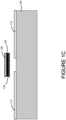
- FIGS. 1A-1C illustrate an example circuit design of a cantilevered out-of-plane RF MEMS switch 100.
- FIG. 1A is a top view of the switch
- FIG. 1B is a cross-sectional view of the switch along axis X
- FIG. 1C is another cross-sectional view of the switch along axis Y.
- the example switch 100 is formed over a coplanar waveguide 101 in which a signal line 110 is formed between ground planes 102, 104 of a substrate 105.
- the signal line 110 includes an input port 112 and an output port 114 formed on opposing ends of the substrate 105.
- the cantilever switch includes a post 120 or anchor affixed to the substrate 105 and includes an extension extending over the substrate in a direction perpendicular to the signal line 110.
- the extension of the cantilever includes a bottom layer 125 of dielectric material, such as silicate, and a top layer 130 of conductive material 130, such as gold.
- the cantilever further includes a contact bump or dimple 135 positioned underneath the bottom dielectric layer 120 and in alignment with the signal line ports 112, 114. Thus, when the cantilever is bent downward, the dimple 135 contacts the signal line 110, thereby connecting the input and output ports 112, 114.
- the switch 100 also includes an electrostatic actuator (not shown) for actuating the cantilever by applying or removing a DC bias voltage between the cantilever and the ground 102, 104 of the coplanar waveguide 101.
- the cantilever bends downward and upward, in a direction towards and away from the signal line respectively, in response to the applied voltage from the actuator.
- Other RF MEMS switches may rely on a lateral movement in order to bring the moveable part of a cantilevered switch towards or away from a contact.
- Each of the moving part and contact may be metal (resistive switch), or one may be metal while the other is dielectric (capacitive switch).
- RF MEMS switches compared to their solid state semiconductor counterparts, exhibit several important advantages such as: superior linearity; low insertion loss; and high isolation.
- RF MEMS switches at millimeter wave frequencies are suitable for use in modem telecommunication systems, especially for automotive radar systems, 5G wireless communication, short range indoor microwave links, wide-band transceivers, phased array systems and high precision instrumentation applications.
- RF MEMS switches Compared with PIN diodes and field-effect transistor (FET) switches, RF MEMS switches have been found to offer lower power consumption, higher isolation, lower insertion loss and higher linearity at a lower cost.
- Prior art CN 105 742 124 discloses an RF MEMS switch with a primary beam in series with the signal line and two secondary beams on the defected ground planes.
- RF MEMS switch performance is prone to electromechanical failure after several switching cycles, especially under hot switching conditions.
- the switch may fail due to static friction (or stiction) buildup.
- the static friction can cause the switch to become stuck. It may require a high voltage to overcome the stiction force. But at low voltage, the switch can remain "welded" to the component.
- An aspect of the present disclosure is directed to a microelectromechanical switch including: a signal line having each of an input port and an output port, the signal line formed on a substrate between a first ground plane and a second ground plane formed on the substrate; a primary deflectable beam having a first end, a second end, and a deflectable middle portion between the first and second ends, the first end supported by a first post formed over the first ground plane, the second end supported by a second post formed over the second ground plane, and the middle portion of the primary deflectable beam positioned over at least a portion of the input port and at least a portion of the output port, whereby the deflectable middle portion contacts each of the input port and output port when deflected downward; one or more defected ground structures formed in each of the first ground plane and the second ground plane; and for each defected ground structure, a corresponding secondary deflectable beam positioned over the defected ground structure.
- the switch may further include a first actuator coupled to the primary deflectable beam and configured to apply a first bias voltage to the primary deflectable beam, whereby the first bias voltage causes the primary deflectable beam to deflect downward toward the signal line, and a second actuator coupled to each of the one or more secondary deflectable beams and configured to apply a second bias voltage to each of the secondary deflectable beams, whereby the second bias voltage causes each secondary deflectable beam to deflect downward toward its corresponding defected ground structure.
- each of the defected ground structures may include a plurality of slots etched into the ground plane and forming a spiral.
- each ground plane may include a first defected ground structure and a second defected ground structure, the length and width of the second defected ground structure being shorter than the length and width of the first defected ground structure.
- the input and output ports may be formed along a first axis of the switch, with the primary deflectable beam extending from the first post to the second post along a second axis perpendicular to the first axis, and the secondary deflectable beams extending in a direction parallel to the first axis.
- each of the secondary deflectable beams may have a first end supported by a first secondary post and a second end supported by a second secondary post.
- a bottom surface of each secondary deflectable beam may be suspended over the ground plane and corresponding defected ground structure by its first and second secondary posts.
- An upper surface of the primary deflectable beam may be less than 4 microns higher than the surface of the signal line.
- An upper surface of each secondary deflectable beam may be less than 2.5 microns higher than the surface of the ground plane.
- the middle portion of the primary deflectable beam may have a plurality of perforations forming a lattice structure.
- the perforations may increase the flexibility of primary deflectable beam.
- Each corner of the middle portion may extend outward toward the first or second end in a serpentine pattern. The extended corners of one side of the middle portion may meet at the first end, while the extended corners of the other side of the middle portion meet at the second end.
- the primary deflectable beam may be less than 150 ⁇ m long and yet sufficiently flexible for the middle portion to deflect 1 ⁇ m or more downward. The downward deflection may be in response to application of a bias voltage, such as a voltage of about 17 volts or less.
- each secondary deflectable beam may include a plurality of perforations forming a lattice structure. The perforations may increase flexibility of secondary deflectable beam.
- the switch may achieve insertion loss of less than -2 dB and isolation of greater than -20 dB between 75 GHz and 130 GHz.
- actuation of the primary deflectable beam and non-actuation of the secondary deflectable beams may result in isolation between the input and output ports of about -24 dB or better between 75 GHz and 130 GHz.
- actuation of the secondary deflectable beams and non-actuation of the primary deflectable beam may result in insertion loss of -1.5 dB or better between 75 GHz and 130 GHz.
- the present disclosure provides for RF MEMS switches having improved signal characteristics and reduced vulnerability to stiction.
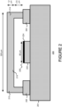
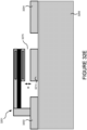
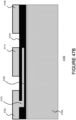
- FIG. 2 shows an RF shunt switch 200 with a doubly-supported cantilever beam 210 formed above a coplanar waveguide formed on a substrate 201.
- a first end 212 and second end 214 of the beam 210 are supported by respective ground planes 202 and 204 formed in the coplanar waveguide .
- the middle of the beam 210 is suspended over a signal line 220 formed in the coplanar waveguide .
- the beam 210 is connected to an actuator (not shown) configured to apply a direct current (DC) bias voltage across the beam 210 the ground planes 202, 204.
- the DC bias voltage causes the beam 210 to deflect downward.
- the signal line 220 includes a conductive layer 222 covered by a thin dielectric layer 224, such as silicon nitride.
- the dielectric layer may be about 0.2 ⁇ m thick.
- the beam 210 is made of molybdenum, and has a length of about 325 ⁇ m, a width of about 60 ⁇ m, and a thickness of about 1.2 ⁇ m.
- the signal line 220 extends through the coplanar waveguide, and has a width (in the direction of the beam length) of about 60 ⁇ m.
- the beam 210 is suspended about 2.5 ⁇ m above the signal line 220, thereby forming a 2.5 ⁇ m air gap.
- the dielectric layer has a thickness of about 0.2 ⁇ m.
- FIG. 3 shows a top view of the switch 200 of FIG. 2 .
- the beam 210 is perforated, having a grid of small perforations 301 in the middle and a large perforation 302, 303 at each end.
- the perforations yield improved downward deflection of the beam 210.
- FIG. 3 further illustrates the vertical displacement of the beam 210 when the DC bias voltage is applied, which is extends from no displacement at the respective ends 212, 214 of the beam, to about 0.91 ⁇ m in the middle of the beam 210.
- the DC bias for the switch of FIG. 2 has been observed to be about 37 V.
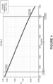
- FIG. 4 shows isolation characteristics of the switch of FIG. 2 when the switch is open, across a band of millimeter wave signals from 75 GHz to 130 GHz. Isolation is about -12.4 dB at 75 GHz, and about -19.7 dB at 130 GHz. Insertion loss of the switch when closed is about 0.74 dB, and return loss is about 10.04 dB.
- switch 500 includes a rectangular beam 510 made of gold and having a perforated structure.
- the middle portion 516 of the beam 510 forms a perforated grid or lattice.
- Each corner of the lattice structure then extends in a serpentine pattern toward the first and second ends 512, 514 of the beam 510.
- the serpentine patterns on either end are then connected to one another, thereby forming first and second serpentine structures on either end of the beam 510.
- the serpentine structure permits for deflection of the beam with a lower bias voltage.
- the dimensions of the switch shown in FIG. 5 is largely comparable to that of FIG. 2 , except that the beam of FIG. 5 is slightly longer (about 345 ⁇ m), and slightly wider (about 65 ⁇ m). The beam still deflects downward up to 0.9 ⁇ m with only a 17 V bias voltage.
- the switch of FIG. 5 also has improved isolation characteristics.
- FIG. 6 shows isolation characteristics of the switch of FIG. 5 when the switch is open, across the 75 GHz to 130 GHz band. Isolation is about -22.0 dB at 75 GHz, and about -14.7 dB at 130 GHz, and drops to as little as about -24.8 dB at 86 GHz. Additionally, insertion loss of the switch when closed is only about 0.6 dB, and return loss is only about 15.15 dB.
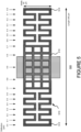
- the example switch 700 of FIG. 7 includes a beam 710 having the same structural arrangement as the beam 510 of FIG. 5 and formed on a ground plane structure 701 measuring about 320 ⁇ m long by about 400 ⁇ m wide.
- the ground plane structure 701 includes a signal line 720 between two ground planes 702, 704.
- a two-dimensional defected ground structure (DGS) is formed in each of the ground planes 702 and 704 of the switch 700.
- the DGS essentially behaves as a band stop filter, thereby affecting the transmission characteristics of the switch 700.
- the DGS forms four spiral shaped slots 731, 732, 733, 734 in a two-by-two grid and having mirror symmetry along the lengthwise axis of the signal line 720.
- each of the spiral shaped slots have a common, uniform width W.
- a first slot 810 extends from the channel 802 separating the signal line from the ground plane. Each subsequent slot connects to the previous slot at a right angle.
- the second slot 820 connects to the first slot 810 at a right angle
- the third slot 830 connects to the second slot at a right angle turning in the same angular direction, thereby forming a spiral.
- the DGS of FIG. 8 includes a total of seven slots formed using the above described spiral pattern.
- the DGS structure also includes an opening connecting the beginning of the first slot to the end of the fourth slot.
- the first four slots of the DGS structure of FIG. 8 also form a rectangular box having a length defined by the second slot and a width defined by the third slot.
- the length and width of the rectangular box may be defined in terms of distances "a" and "b" in which "a” is the length of the third slot, and "b” is the difference in length between the second slot and third slot (hence the length of the second slot is equal to a+b).
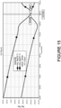
- FIG. 9 shows insertion loss and return loss of the switch 700 when the switch is closed. Insertion loss is about -2.2 dB at 75 GHz, about -10.4 dB at 130 GHz, but drops as low as -16.6 dB at 105 GHz. Return loss is about -24.0 dB at 75 GHz, and about -11.2 dB at 130 GHz, but increases to as much as about -9.5 dB at 105 GHz.
- FIG. 10 shows isolation for the switch 700 when the switch is open. Isolation is about -17.1 dB at 75 GHz and about -11.5 at 130 GHz, and drops as far as about - 32.5 dB at 82 GHz.
- FIG. 9 shows that including the DGS in the ground plane of the switch results in higher insertion loss.
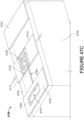
- FIG. 11 an improvement to the DGS structures of the FIG. 7 switch is shown in FIG. 11 .
- the switch 1100 of FIG. 11 is largely similar in structure to that of FIG. 7 .
- the switch 1100 has two ground planes 1102, 1104 bisected by a signal line 1120 and has four DGS structures 1131, 1132, 1133, 1134 formed in the ground planes.
- the length of the ground planes and signal line are about 340 ⁇ m, and the cumulative width of the switch is about 404 ⁇ m.
- Switch 1100 differs from FIG. 7 in that each of the DGS structures includes a secondary MEMS switch 1141, 1142, 1143, 144 positioned above the DGS structure.
- the shape of both the secondary switch and DGS may be rectangular, but the secondary switch may be longer while the DGS structure may be wider. In the example of FIG.
- each DGS structure is a perforated lattice, and is about 105 ⁇ m in length and about 85 ⁇ m in width, and overlaid by a secondary switch that is about 139 ⁇ m in length and 65 ⁇ m in width.
- FIG. 12 A side view of a single DGS structure of the switch 1100 is shown in FIG. 12 , although the DGS structure itself is not shown.
- the switch 1100 includes a substrate 1101 on which the ground plane 1102 is formed.
- the ground plane 1102 has a thickness or height of about 2 ⁇ m.
- the slots of the DGS structure 1131 are formed in the ground plane, and may have a depth equal to the height of the ground plane 1102.
- a secondary switch 1141 is formed above the DGS structure 1131.
- the secondary switch 1141 includes a beam 1151 supported by two feet 1162, 1164.
- the supporting feet have a height of about 1 ⁇ m, thereby raising the beam 1151 about 1 ⁇ m above the DGS and ground plane.
- the beam thickness or height of the beam 1151 may be about 1.2 ⁇ m.
- the beam 1151 is connected to an actuator (not shown) to supply a bias voltage, which runs from the beam 1151 to the ground plane 1102 via the feet 1162, 1164. Applying the bias voltage causes the beam 1151 to deflect downward towards the ground plane 1102, thereby affecting the capacitive characteristics of the DGS structure 1131.
- the amount of voltage applied to the switch 1101 may be continuously variable, and thus the capacitive characteristics of the DGS structure (and its effect on the main MEMS switch of the device) can be varied or tuned.
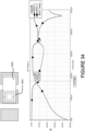
- the switch arrangement of FIG. 11 behaves like a metamaterial. This can be seen by first analyzing the transmission and reflection phases of a signal line formed in a coplanar waveguide without the DGS structure of FIG. 11 , and then analyzing the transmission and reflection phases of the same signal line with the DGS structure of FIG. 11 .
- FIG. 13 shows transmission and reflection phases of a signal transmitted across a coplanar waveguide without the DGS structure over a band of millimeter wave frequencies from 50 GHz to 140 GHz. As seen in FIG. 13 , any shift in the transmission phase of the signal is met with a substantially equal (within about 20 degrees) shift in the reflection phase.
- FIG. 14 shows transmission and reflection phases of a signal over the same band of frequencies for the same coplanar waveguide but with the DGS structure incorporated into the waveguide at a height of 2.2 ⁇ m, which is the distance from the top surface of the substrate (the basin of the slots of the DGS structure) to the bottom surface of the secondary switch positioned above the DGS structure.
- the transmission and reflection phases do not shift equally across the band of frequencies, and even shift in opposite directions, eventually crossing one another at 85 GHz and then crossing back at 96 GHz.
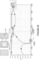
- FIG. 15 shows transmission and reflection phases for the same coplanar waveguide but with the DGS structure at a height of 2.6 ⁇ m.
- the transmission and reflection phases shift substantially equally until about 110 GHz, but then begin shifting in opposite directions at frequencies above 115 GHz and even cross one another at about 128 GHz.
- the particular resonance frequency of the DGS structure can vary depending on the height of the air gap between the ground plane and the beam.
- FIG. 16 shows a plot of isolation characteristics for five secondary switches positioned over DGS structures at varying heights. The resonant frequency of the structure is shown to shift to higher frequency as the air gap between the ground plane and beam increases.
- the switch 1700 includes a signal line 1720 positioned between a first ground plane 1702 and a second ground plane 1704, the signal line separated from each ground plane by first and second spaces 1703, 1705, respectively.
- a primary shunt switch 1710 is positioned on top of, is connected to, and bridges the first and second ground planes 1702, 1704.
- the primary shunt switch 1710 runs perpendicular to, and is suspended over, the signal line 1720.
- the switch 1710 deflects downward toward the signal line 1720.
- the switch 1710 deflects back upward to its original position.
- a first DGS structure 1731 and a second DGS structure 1732 are formed in the first ground plane 1702.
- a third DGS structure 1733 and a fourth DGS structure 1734 are formed in the second ground plane 1704.
- the first and third DGS structures 1731, 1733 have mirror symmetry along a lengthwise axis X of the primary switch 1710, and are a similar shape.
- the second and fourth DGS structures 1732, 1734 also have mirror symmetry along a lengthwise axis X of the primary switch 1710, and are a similar shape.
- the first and third DGS structures 1731, 1733 are a different size from the second and fourth DGS structures 1732, 1734.
- the second slots of the first and third DGS structures 1731, 1733 are about 85 ⁇ m long, whereas the second slots of the second and fourth DGS structures 1732, 1734 are about 100 ⁇ m long.
- the third slots of the first and third DGS structures 1731, 1733 are also shorter than those of the second and fourth DGS structures 1732, 1734. This is in contrast to the four DGS structures shown in each of FIGS. 7 and 11 , which all have the same dimensions
- the dimensions of the different DGS structures can be characterized in terms of lengths "a,” “a1,” and “b,” whereby a is the length of the third slot in one DGS structure, a1 is the length of the third slot in the other DGS structure, and b is the difference in length between the second and third slots in one or both size DGS structures.
- the differently sized DGS structures may be designed to have the same value "b,” such that the difference between the second and third slot lengths is the same for each structure even when the structures are of different sizes.
- Each DGS structure is overlaid by a respective secondary shunt switch 1741, 1742, 1743, 1744.
- Each secondary shunt switch is connected to its respective ground line, and is suspended over its respective DGS structure with an air gap in between.
- the secondary shunt switches are rectangular, each of the secondary switches positioned lengthwise parallel to the signal line 1720 and perpendicular to the primary shunt switch 1710.
- the secondary switches positioned above the first DGS structure 1731 and the third DGS structure 1733 have a mirror symmetry with the secondary switches positioned above the second DGS structure 1732 and the fourth DGS structure 1734 along a lengthwise axis X of the primary switch 1710.
- the secondary switches positioned above the first DGS structure 1731 and the second DGS structure 1732 have a mirror symmetry with the secondary switches positioned above the third DGS structure 1733 and the fourth DGS structure 1734 along a lengthwise axis Y of the signal line 1720.
- the secondary shunt switches 1741, 1742, 1743, 1744 are also perforated. In the example of FIG. 17 , the switches have a grid-like lattice perforation.
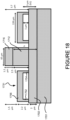
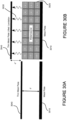
- FIG. 18 shows a side view of the switch of FIG. 17 from the viewpoint along either side of FIG. 17 .
- the switch 1700 is formed on a substrate 1701.
- a ground plane 1702 is formed over the substrate 1701, and the primary switch 1710 is formed on top of the ground plane 1702.
- the primary switch 1710 has two feet 1712 (the second foot is obstructed by foot 1712 in FIG. 18 ) supporting a beam 1716.
- Two secondary switches 1731, 1732 are positioned on either side of the primary switch 1710.
- Each of the secondary switches also includes two feet 1752, 1754 supporting a beam 1756.
- DGS structures (not shown) are formed in the ground plane 1702 at respective positions underneath the secondary switches 1731, 1732.
- the substrate and ground planes have a length of about 404 ⁇ m, and a width of about 340 ⁇ m.
- the ground planes have a thickness of about 2 ⁇ m.
- the primary switch 1710 extends the length of the substrate, and the primary switch feet 1712 and beam 1716 have a width of about 65 ⁇ m.
- the feet 1712 have a height of about 2.5 ⁇ m, and the beam 1716 has a thickness of about 1.2 ⁇ m.
- the secondary switches 1731 have a length of about 139 ⁇ m, and the secondary switch feet 1752, 1754 and beam 1756 have a width of about 65 ⁇ m.
- the feet 1752 have a height of about 1 ⁇ m, and the beam 1756 has a thickness of about 1.2 ⁇ m.
- the entire switch 1700 can be formed on top of the substrate 1701 within a 5.7 ⁇ m space.
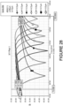
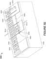
- FIG. 19 shows an example layout of a switch 1900, showing the connections between the primary switch 1910 and secondary switches 1941-1944, a first actuator 1962, and a second actuator 1964.
- the first actuator 1962 is connected to the primary switch 1910 and configured to provide a bias voltage to the primary switch.
- the second actuator 1964 is connected to each of the secondary switches 1941-1944 and is configured to provide a bias voltage to the secondary switches.
- the primary switch 1910 may be either ON (bias voltage provided from the first actuator 1962) or OFF (no bias voltage provided by the first actuator 1964).
- the primary switch When the primary switch is ON, the primary switch beam deflects downward, resulting in a large shunt capacitance that blocks RF signals from propagating along the signal line 1920.
- the primary switch When the primary switch is OFF, the primary switch beam deflects back upward (at rest), reducing the shunt capacitance and permitting RF signals to propagate along the signal line 1920.
- the secondary switches 1941-1944 may be turned ON in order to negate the effects of the DGS structures towards insertion and return loss.
- a bias voltage is applied from the second actuator 1964 to each of the secondary switches 1941-1944, thereby causing the switches to deflect downward toward the DGS structures and create a shunt capacitance blocking the effects of the DGS structure.
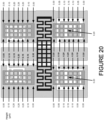
- FIG. 20 shows the amount of downward deflection at several points of the secondary switches (measured in ⁇ m) when the secondary switches are actuated.
- FIG. 21 shows return loss and insertion loss characteristics for the switch 1900 when the primary switch is OFF and the secondary switches are ON.
- insertion loss is as low as about -0.6 dB and return loss is as low as about -21.1 dB.
- insertion loss is still relatively low at about -1.5 dB, and return loss is also relatively low at -14.5 dB.
- FIG. 22 shows the amount of downward deflection at several cross-sections of the primary switches (measured in ⁇ m) when the primary switch is actuated. Deflection along the entire width of the primary switch is uniform for any given point along the length of the switch.
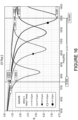
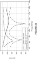
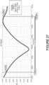
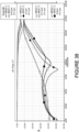
- FIGS. 23-25 show isolation characteristics for the switch 1900 when the primary switch is ON and the secondary switches are OFF.
- the same DGS structure is used. This leads to a significant improvement of isolation at a relatively narrow band (e.g., less than about 10 GHz, between 90 GHz and 100 GHz).
- isolation is about -23.1 dB, and at 130 GHz, isolation is about -23.9 dB. But at about 95 GHz, isolation is improved to about -52 dB.
- FIGS. 24 and 25 different DGS structures are used. This leads to an overall improvement of isolation over a wider band of frequencies.
- the structure represented in FIG.24 yields improved isolation at about 84 GHz (about -51 dB) and at about 112 GHz (about -59 dB), and is not worse than about -24 dB between 75 and 130 GHz.
- the structure represented in FIG. 25 achieves its best isolation at about 98 GHz (about -41.5 dB), but the improved isolation characteristics do not sharply drop off. In this regard, isolation of -30 dB or better can be achieved across a wide band of frequencies, from about 85 GHz to about 110 GHz.
- DGS structures with capacitive shunt switches above the DGS structures is an effective way of incorporating the benefits of DGS for improved isolation when RF signals are blocked, while at the same time negating the detriments caused by the DGS to insertion loss and return loss when RF signals are propagating.
- incorporation of DGS structures and corresponding shunt switches is an improvement to RF MEMS design and operation.
- Table 1 below provides a summary of the actuation voltage, isolation and insertion loss characteristics for the above-described switch designs with air gaps (and cantilever beam heights) of about 2.5 ⁇ m:
- the particular dimensions of the RF MEMS switches, structures, and waveguide components may be altered without deviating from the core concepts of the present disclosure.
- the substrate, ground plane and signal line may be made longer or shorter, wider or narrower, and thicker or thinner.
- the primary and secondary switches may be designed in different shapes having different lengths, different widths, or different patterns, such as to enable a desired amount of deflection.
- the air gap between switches and the components positioned underneath may be altered.
- the shape and size of the DGS structures may also be altered.
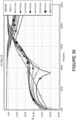
- FIG. 26 shows isolation characteristics for several switches having different DGS and secondary switch arrangements, in which both switches are actuated. Actuating the secondary switch results in improved isolation characteristics over a narrow band of frequencies. The particular band at which the improved isolation occurs varies depending on the air gap height between the switches and DGS structures. As the air gap increases, the frequency band at which the best isolation for the switch occurs shifts upward.
- the electric field of the switch can be increased by distancing the top electrode from ground. This can be accomplished, for example, by sandwiching the conductive layer (e.g., gold) between two dielectric layers (e.g., silicon oxynitride).
- the beam can be modified to maximize its restoring force without having to increase the bias voltage.
- Improved restoring force is influenced by such parameters as increased plate size, shortened beam length, or increased dielectric thickness.
- FIG. 29 is a force diagram illustration of an experimental setup 2900, in which a plane of metal 2910 is positioned in parallel to a metamaterial 2920. The metal and metamaterial are positioned apart from one another at a distance "d.” The forces illustrated in the setup 2900 are shown using arrows 2930. A first force applied to the metal 2910 and metamaterial 2920 brings the two planes closer to one another. However, application of this first force has been observed under the specific conditions of the experimental setup 2900 to result in a second and opposite force "F" that causes the two planes to separate from one another.
- F second and opposite force
- the Casimir force originates from the interaction of the surfaces with the surrounding electromagnetic spectrum, and exhibits a dependence on the dielectric properties of the surfaces and the medium between the surfaces. Casimir forces between macroscopic surfaces have the same physical origin as atom-surface interactions and those between two atoms or molecules (van de Waals forces), because they originate from quantum fluctuations.
- the Casimir force is known to be proportional to the effective permittivity of metal plates. Therefore, by decreasing the effective permittivity on the metal planes, the Casimir force too can be decreased. This can result in reduced forces preventing the plates from separating from one another, thus at least partially mitigating the stiction problem observed in MEMS switches.
- a repulsive force can actually be generated between the planes if the effective permittivity is sufficiently decreased, such as by using metamaterials.
- This repulsive force is sometimes referred to as the "repulsive Casimir force,” and in the present application can further be used to resolve the stiction issue by repelling the contacts from one another.
- generating a repulsive Casimir force can result in even less of a liability for the contacts to effectively become "welded" together due to stiction.
- Casimir interactions may be realized in engineered materials such as silicon crystals, which can be used for levitation, microwave switches, MEMS oscillators and gyroscopes.
- Casimir interaction is attractive in magnetic Metamaterials made of nonmagnetic meta-atoms. In contrast, intrinsically magnetic meta-atoms could potentially lead to Casimir repulsion.
- Chiral Metamaterials made of metallic and dielectric metaatoms are good candidates for Casimir repulsion.
- One approach is to engineer the material combinations that give rise to Casimir repulsive forces. For example, Casimir repulsive forces have been observed between multilayer walls made of alternating layers of a topological insulator (TI) and a normal insulator.
- TI topological insulator
- the force may turn into repulsion in the TI multilayer structure, and in the region of repulsion for semi-infinite TI, the repulsive force can be enhanced in magnitude, the enhancement tends to a maximum while the structure contains sufficiently many layers.
- Casimir forces between macroscopic surfaces entail separations typically > 0.1um where retardation plays an essential role, while van der Waals forces refer to separations ⁇ 0.0lum where retardation is insignificant.
- Advances in theoretical studies and experimental techniques have enabled examination of the Casimir force beyond the configuration of two parallel perfect metal plates. Novel materials and shapes of the interacting bodies enable new opportunities for applications and, at the same time, pose new open questions.
- MTM-Inspired structures can produce a powerful Casimir Effect, which will allow transportation of matter; this implies, in principle, that the effect can be used to attract or push away physical matter.
- a further complexity of the Casimir force potentially allows greater opportunity for neutralization or for use of Casimir forces to partially cancel Van Der Waals forces.
- polaritonic involvement causes a repulsive Casimir force between Metal and MTM structures.
- binding TM polaritons govern at shorter distance, inundated by joint repulsion due to anti-binding TM and TE polaritons.
- surface plasmons can be indicative of the strength and sign of the Casimir force.
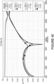
- FIGS. 30A and 30B show a typical example of a levitating mirror.
- the repulsive Casimir force of the metamaterial may balance the weight of one of the mirrors, letting it levitate on zero-point fluctuation.
- FIG. 30A shows a first metal plate 3010 or mirror separated from a second metal plate 3040 or mirror by a distance d.
- the two metal plates may be thought of as opposing contacts in a MEMS switch, and may be liable to become permanently stuck to one another at distances "d" that are sufficiently small.
- FIG. 30B shows a thin layer of metamaterial 3020 affixed to a surface of the first metal plate 3010 and positioned in between the metal plates 3010, 3040.
- a Casimir force 3030 is produced at the boundary between the metamaterial 3020 and the second metal plate 3040, thereby causing the second metal plate to further separate from the first metal plate 3010 by a distance d'. This additional separation may even counteract gravitational forces, and thus cause the second metal plate 3040 to levitate.
- the metamaterial may be made from gold foil.
- the switch may include a deflectable beam having a shorting bar positioned on a surface of the beam and aligned with the contact of the signal line.
- the shorting bar may be made of metal, such as a thin layer of gold foil located.
- the metal-to-metal contact surfaces may stick to one another in the form of strong adhesion. This adhesion causes undesirable stiction problems, which in turn may cause the switch to be electrically shorted, and it may take a considerable amount of force to separate the shorting bar from the signal line.
- the RF MEMS switch generally relies on stresses accumulating in the beam as a result of the beam's deflection in order to counteract the adhesive forces and to return the beam back to its at-rest or equilibrium position.
- This counteractive force which is the sum of the stresses in the beam, is referred to as the restoring force that "restores" the beam to its at-rest position.
- this force is not always sufficient to counteract adhesive forces between the metal contacts.
- the restoring force of the beam can be supplemented using the repulsive Casimir force generated when the shortening bar touches or comes within proximity to the signal line.
- the Casimir force can be controlled by providing a permittivity gradient in the contact of the deflectable beam.
- the permittivity gradient can be provided by interfacing three layers of media in either decreasing or increasing order of permittivity.
- three layers of media are provided: a first layer 3110 having permittivity ⁇ 1 , a second layer 3120 having permittivity ⁇ 2 , and a third layer 3130 having permittivity ⁇ 3 .
- the first and third layers may be metal layers, and the second layer may be a dielectric layer.
- the layers may be interfaced such that either ⁇ 1 ⁇ ⁇ 2 ⁇ ⁇ 3 or ⁇ 1 > ⁇ 2 > ⁇ 3 .
- the first layer 3110 may be made of gold and have an infinite permittivity
- the second layer 3120 may be made of a dielectric (e.g., silicon mononitride (SiN)) and have a small but positive permittivity (e.g., 7)
- the third layer 3130 may include a metamaterial unit cell 3135 and may have a zero or even negative permittivity.
- the first layer 3110 can also include a metamaterial unit cell 3115 in order to acquire the desired permittivity.
- FIGS. 32A-E are illustrations of an example RF MEMS switch 3200 incorporating metamaterial cells in order to provide a repulsive Casimir force between contacts of the switch.
- FIG. 32A is a top-down view of the switch
- FIG. 32B is a perspective view of the switch
- FIG. 32C is a bisected cross-sectional perspective view of the switch
- FIG. 32D is a side view of the switch in a closed position
- FIG. 32E is a side view of the switch in an open position.
- the switch is formed in a coplanar waveguide 3201 positioned having two ground planes 3202 and 3204 formed above a substrate 3205.
- the ground planes are separated by a channel and a signal line 3210 is formed lengthwise in the channel.
- the signal line 3210 includes each of an input port 3212 through which a signal is received (arrow in) and an output port through which the signal is transmitted (arrow out).
- the switch includes a cantilevered beam that moves in and out of the plane of the coplanar waveguide in order to move in and out of contact with the signal line 3210.
- the beam includes multiple layers.
- the layers include: a top layer 3420 of dielectric material, a first metal layer 3210, a dielectric layer 3220, and a second metal layer 3230.
- Each of the first and second metal layers 3210, 3220 may include a metamaterial device 3215, 3235 encased within, as shown in the cross-sectional view of FIG. 32C .
- the top layer 3210 and first mater layer 3220 may be adapted to extend across the entire length of the beam, whereas the length of the sandwiched dielectric layer 3220 and second metal layer 3230 may be limited to the area above the signal line 3210.
- the dielectric layer 3220 may extend the entire length of the beam while only the second metal layer 3230 may be limited to the area above the signal line 3210.
- ground planes 3202, 3204 and signal line ports 3212, 3214 may be separated from the substrate 3205 by a thin layer of dielectric 3250, such as SiN or SiO 2 .
- Operation of the switch may be controlled by moving an anchor 3270 to which the beam is attached in and out of the plane of the coplanar waveguide 3201.
- the ground line 3202 may include a hole 3260 though which a post or anchor 3270 of the beam is positioned. Moving the post 3270 up and down can result in the contacts of the switch separating or contacting one another, respectively.
- FIG. 32D shows the switch closed, with the contacts contacting one another.
- FIG. 32E shows the switch open, with the dielectric and metal layers of the beam elevated above the signal line ports 3214, thereby forming a gap 3275 of a given height H.
- the section of the coplanar waveguide shown may be about 100 ⁇ m, and the beam may have a width of about 75 ⁇ m.
- the anchor 3270 to which the beam is attached may have a length (in the direction of the beam length) of about 11.25 ⁇ m and a width of about 75 ⁇ m.
- the opening 3260 into which the beam is anchored may have a greater length and width, such as about 80 ⁇ m by 30 ⁇ m.
- the overall length of the waveguide (in the direction of the beam length) may be about 330 ⁇ m, whereby the ground planes and the signal lines may each have a width (also in the direction of the beam length) of about 75 ⁇ m, with 38 ⁇ m channels in between.
- the beam may have a length of about 140 ⁇ m (not including the length of the anchor 3270).
- the overall height of the beam when in the closed position may be about 5 ⁇ m, relative to the dielectric surface on which the ground planes and signal line are formed. Each of the ground planes and signal line may be 2 ⁇ m thick.
- the beam may then contribute an additional 3 ⁇ m to the height of the switch, whereby each of the metal layers 3210, 3230 is about 1 ⁇ m thick and the dielectric layer 3220 sandwiched in between may also be about 1 ⁇ m.
- the top layer 3440 may add about an additional 0.2 ⁇ m to the height of the switch.
- the height of the switch may increase by H when open, as shown in FIG. 32E .
- the metamaterial unit cells included in the second metal layer 3230, and optionally in the first metal layer 3210 as well, may have the shape of a split ring resonator.
- the split rings may be square-shaped.
- FIG. 33 illustrates an example metal layer 3310 having each of a first split ring 3322 having width L, and a second split ring 3324, formed in the layer, whereby forming the rings may involve cutting out the rings from the layer.
- Each of the rings may be concentric, and may be aligned so that the splits 3330 in the respective rings are positioned on opposing sides of the layer 3310.
- Each of the rings may have a uniform width W, and the splits 3330 may have a uniform width G.
- the rings may further be separated from one another by a uniform separation 3332 having width S.
- FIGS. 34-36 provides simulated test results for transmission and reflection characteristics for a respective unit cell structure.
- the simulated test results were collected using Matlab code, although other programs could be used to run simulations in other cases.
- the metamaterial structure 3401 of FIG. 34 is included in a metal layer having a width equal to the width of the beam 3402.
- the unit cell is of transmission type at low frequencies, at about 300 GHz and again at about 470 GHz.
- the unit cell is of reflection type, with attenuation of the transmission exceeding that of the reflection, at about 150 GHz, and again at about 300 GHz.
- the structure of FIG. 34 is shown to exhibit metamaterial properties.
- the metamaterial structure 3501 of FIG. 35 is included in a metal layer having a length equal to the width of the signal line, and further attached to a beam 3502 having a width much smaller than the width of the metal layer.
- the unit cell is shown to have transmission properties at about 54 GHz and reflection properties at about 150 GHz. Therefore, the structure of FIG. 35 is also shown to exhibit metamaterial properties.
- the metamaterial structure 3601 of FIG. 36 is included in a metal layer having a length equal to the width of the signal line, and further attached to a U-shaped beam 3602 having two branches each having width much smaller than the width of the metal layer.
- the unit cell is shown to have transmission properties at about 80 GHz and reflection properties at about 163 GHz. Therefore, the structure of FIG. 36 is also shown to exhibit metamaterial properties, and these properties can be exhibited over a relatively narrow bandwidth of about 83 GHz.
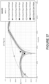
- FIG. 37 provides a graph plotting reflection characteristics for a metamaterial cell having different parameters G, S and W (as defined in connection with FIG. 33 above).
- G, S and W as defined in connection with FIG. 33 above.
- the frequency at which reflection is most greatly attenuated varied from about 80 GHz to about 90 GHz depending on G, S and W.
- G, S, and W is 9 ⁇ m
- insertion loss drops to about -74 dB at 80 GHz.
- other parameters of G, S, and W yield a reflection of about - 60 dB at about 90 GHz.
- the metal layers of the MEMS switch may also be formed with different parameters and dimensions as compared to those parameters and dimensions described above.
- FIG. 38 is a plot of both transmission and reflection properties of a switch for which the thickness of the second metal layer "d" ( e.g., 3230 of FIGS. 32A-E ) varies between 0.5 ⁇ m through 2 ⁇ m.
- FIG. 39 is a plot of transmission and reflection properties of a switch for which the thickness of the sandwiched dielectric layer ( e.g., 3220 of FIGS. 32A-E ) varies between 1.5 ⁇ m through 5 ⁇ m.
- FIG. 38 is a plot of both transmission and reflection properties of a switch for which the thickness of the second metal layer "d" ( e.g., 3230 of FIGS. 32A-E ) varies between 0.5 ⁇ m through 2 ⁇ m.
- FIG. 39 is a plot of transmission and reflection properties of a switch for which the thickness of the sandwiched dielectric layer ( e.g.
- the thickness of the first metal layer "d1" e.g., 3210 of FIGS. 32A-E .
- the transmission properties of the various MEMS switches are largely similar in each of these conditions, although the frequency at which the transmission attenuates varies between about 160 GHz and about 180 GHz, and the reflection properties of the switch vary mainly between 60 GHz and 150 GHz.
- permeability and permittivity of the metamaterial cells can be extracted using parameter extraction procedures known in the art.
- the parameter extraction is shown in FIG. 41 .
- the metamaterial structure exhibits near zero permittivity as well as permeability at a band of frequencies centered around 80 GHz. Therefore, it is clear from FIG. 41 that these structures would produce a repulsive Casimir force around the band of frequencies ranging from about 60 GHz to about 130 GHz.
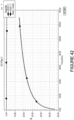
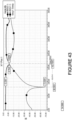
- FIGS. 42 and 43 further demonstrate the overall response of the RF MEMS switch in each of its ON and OFF states, respectively.
- the reflection characteristics are shown to be just slightly less than 0 dB even at frequencies of up to 130 GHz, and the transmission characteristics are between about -20 dB and -15 dB between operating frequencies of about 60 GHz to about 130 GHz.
- the reflection characteristics are as low as about -73.5 dB at 80 GHz with the transmission characteristics as high as -0.33 dB while the reflection and transmission characteristics at 163 GHz are both about -6.75 dB.
- FIGS. 32 through 43 demonstrate the possibility of incorporating metamaterials into a high frequency resistive MEMS switch in order to reduce the effects of stiction.
- the above principles can be similarly applied to capacitive MEMS switches.
- a sandwich of metal and dielectric layers may be used to achieve the desired permittivity interface, such as having a gold layer with infinite permittivity, a dielectric layer with positive but low permittivity, and a metamaterial layer with a permittivity in the range of about zero or less.
- the metamaterial layer may be provided as part of the signal line contact instead of as part of the beam contact.
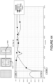
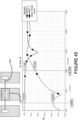
- FIGS. 44-46 provides simulated test results for transmission and reflection characteristics for a respective unit cell structure.
- the simulated test results were collected using Matlab code, although other programs could be used to run simulations in other cases.
- the metamaterial structure 4401 of FIG. 44 is included in a metal layer (e.g., of a signal line contact) and interfaces beam 4402.
- the beam is thinner than the metamaterial structure, and is supported by a single support extending from one of the ground planes adjacent the signal line.
- the unit cell is of transmission type at about 34 GHz (having reflection characteristics of -88.75 dB and transmission characteristics of -0.29 dB).
- the unit cell is of reflection type at about 120 GHz.
- the structure of FIG. 44 is shown to exhibit metamaterial properties.
- the metamaterial structure 4501 of FIG. 45 is included in a metal layer (e.g., of a signal line contact) and interfaces beam 4502.
- the beam is thinner than the metamaterial structure, and is doubly supported by posts on either side of the signal line.
- the unit cell is of transmission type at about 40 GHz (having reflection characteristics of -54 dB and transmission characteristics of -0.5 dB).
- the unit cell is of reflection type at about 140 GHz.
- the structure of FIG. 45 is shown to exhibit metamaterial properties.
- FIG. 46 includes two metamaterial structures 4601 and 4603 positioned at opposing input and output sides of the signal line.
- Each metamaterial structure 4601, 4603 is included in a metal layer ( e.g., of the signal line contact).
- a respective doubly-supported beam 4602, 4604 is positioned above each of the metamaterial structures 4601, 4602.
- the beams are thinner than the metamaterial structures.
- the unit cell is of transmission type at about 8 GHz (having reflection characteristics of -60 dB and transmission characteristics of -0.01 dB).
- the unit cell is of reflection type at about 160 GHz.
- the structure of FIG. 45 is shown to exhibit metamaterial properties.
- FIGS. 47A-C Another example switch 4700 is shown in FIGS. 47A-C.
- FIG. 47 is a top-down view of the switch.
- FIG. 47B is a side view of the switch.
- FIG. 47C is a perspective view of the switch.
- the switch includes a structure formed over a signal line having an input side 4712 and an output side 4714.
- a metamaterial structure having an outer split ring 4722 and inner split ring 4724 is formed in the signal line contact between the input side 4712 and output side 4714, through which a signal is received (arrow in) and an output port through which the signal is transmitted (arrow out).
- the structure of FIG. 47A-C has a width W, a split width of G, and the space between the rings has a width S.
- the signal line has a width L, and the channel separating the signal line from the respective ground planes has a width C.
- Each of the ground planes 4702, 4704 and the signal line are formed from a conductive material such as gold, and are formed on top of a dielectric material 4740 such as silicon nitride (Si 3 N 4 ), which itself is formed on top of a substrate 4705.
- a dielectric material 4740 such as silicon nitride (Si 3 N 4 ), which itself is formed on top of a substrate 4705.
- One of the ground planes 4702 includes a post 4770 extending downward from the ground plane 4702 into the dielectric material 4740, and a beam 4780 extending from the post 4770 in the direction of the signal line 4714.
- the edge of the beam 4780 is aligned with the opposing edge of the signal line 4712, 4714, such that the end of beam 4780 is positioned underneath the metamaterial structures 4722, 4724, of the signal line 4712, 4714.
- the post 4770 can be seen through an opening 4760 in the ground plane 4702.
- the ground planes and the signal line may each have a width (in the direction of the beam 4780 length) of about 73 ⁇ m and the beam may have a length of about 168 ⁇ m.
- the metamaterial structure formed on the signal line contact may have a ring width W of about 15 ⁇ m, a split width G of about 8 ⁇ m, and a spacing between rings S of about 5 ⁇ m.
- Transmission and reflection characteristics of the switch 4700 over a range of frequencies are shown in FIG. 48 .
- the metamaterial is most reflective at about 175 GHz and most transmissive at about 80 GHz.
- a material parameter extraction can be performed in order to determine the permittivity and permeability of the metamaterial structure.
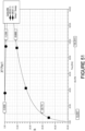
- the extraction is shown over a range of frequencies in FIG. 49 .
- the metamaterial structure exhibits near zero permittivity and permeability between about 50 GHz and 150 GHz. This indicates that the structure of FIG. 48 is suitable for reducing Casimir forces (or even generating repulsive Casimir forces) in the desired frequency band of the present disclosure.
- FIG. 50 shows a perspective view of a capacitive shunt RF MEMS switch 5000 utilizing a metamaterial signal line contact in order to reduce stiction in the switch.
- Much of the features of switch 5000 may be compared to those of switch 4700 in FIGS. 47A-C (ground planes 5002 and 5004 and substrate 5005 compare to planes 4702 and 4704 and substrate 4705; signal line input and outputs 5012 and 5014 compare to 4712 and 4714; split ring metamaterial structure 5022 and 5024 compares to structure 4722 and 4724; dielectric layers 4740 and 5040 are comparable; openings 4760 and 5060 are comparable; posts 4770 and 5070 are comparable; and beams 4780 and 5080 are comparable).
- the switch 5000 further includes a deflectable beam 5050.
- the beam 5050 may be comparable to the rectangular beam 510 described in connection with FIG. 5 ( e.g., may be made from gold, may have a perforated grid structure, may extend in a serpentine pattern).
- the deflectable beam 5050 is supported by a pair of posts formed on top of the ground planes 5002 and 5004, respectively, and is configured to deflect downward towards the signal line when actuated by a bias voltage.
- the bias voltage causes a midpoint of the beam 5050 to deflect downward until it comes in contact with the signal line contact, thereby causing the signal line to turn off (or in other cases to turn on).
- the midpoint of the beam 5050 deflects back upward. Because the midpoint of the beam is aligned with the metamaterial structure 5022, 5024 of the signal line contact, the Casimir effect at the interface between the beam and the signal line contact is diminished or even repulsive, thereby reducing the liability of stiction between the beam 5050 and the signal line.
- the signal line contact may further include a later of dielectric material above the metal layer including the metamaterial structure.
- the dielectric layer may be made of SiN, and may function as an isolation layer in order to achieve the desired permittivity gradient, as discussed above in connection with FIG. 31 .
- the beam 5050 may have an infinite permittivity
- the isolation layer may have a positive but smaller permittivity
- the metal layer including the metamaterial structure in the signal line contact may have a near zero, zero or even negative permittivity, thereby satisfying the ⁇ 1 ⁇ ⁇ 2 ⁇ ⁇ 3 condition (or vice versa).
- FIGS. 51 and 52 are plots of both reflection and transmission characteristics of the switch across a range of high RF frequencies.
- FIG. 51 demonstrates operation of the switch in the ON state (transmitting signals)
- FIG. 52 demonstrates operation of the switch in the OFF state (cutting off transmission of signals)
- the switch is off, thus changing to being reflective instead of transmissive.
- insertion loss is as high as about -22.2 dB while return loss is as low as about -0.26 dB.
- return loss is as low as about -0.26 dB.
- insertion loss is as high as -14.9 dB while return loss is only about -0.82 dB. This demonstrates good operation of the switch in its OFF state across nearly the same wide range of high frequencies, from about 20 GHz to 100 GHz.
- the switches described in the present disclosure can improve operation and performance of applications requiring high frequencies (e.g., 10 GHz or greater) over a wide bandwidth.
- Such technologies may include, but are not limited to, 5G communications, switching networks, phase shifters (e.g., in electronically scanned phase array antennas) and Internet of Things (IoT) applications.
- metamaterial structures described are split rings. However, those skilled in the art should recognize that other metamaterial structures may be used, provided that those structures provide similar permittivity and permeability characteristics within the desired range of frequencies.
- a topology inspired Möbius transformation MTM (metamaterial) structures meaning a structure that forms a continuous closed path that maps onto itself, or stated another way, the structure may have a topology in which a closed path extends two or more revolutions around an axis (e.g., at or close to the center of the structure) before the closed path is completed) may be considered advantageous for generating repulsive Casimir forces.
Claims (5)
- Un commutateur microélectromécanique (1100) comportant :une ligne de signal (1720) comportant chaque accès parmi un accès d'entrée et un accès de sortie, la ligne de signal (1720) étant formée sur un substrat entre un premier plan de masse (1702) et un second plan de masse (1704) formés sur le substrat ;une poutre primaire déviable (210, 1710) ayant une première extrémité (212), une seconde extrémité (214) et une partie centrale déviable entre les première et seconde extrémités, la première extrémité (212) étant supportée par une première borne (1712) formée sur le premier plan de masse (1702), la seconde extrémité (214) étant supportée par une seconde borne formée sur le second plan de masse (1704), et la partie centrale (1716) de la poutre primaire déviable (1717) positionnée sur au moins une partie de l'accès d'entrée et au moins une partie de l'accès de sortie, en sorte que la partie centrale déviable (1716) est en contact avec chaque accès parmi l'accès d'entrée et l'accès de sortie lorsqu'elle est déviée vers le bas ;une ou plusieurs structures à plan de masse démétallisé (1731, 1732, 1733, 1734) formées dans chaque plan parmi le premier plan de masse (1702) et le second plan de masse (1704) ;pour chaque structure à plan de masse démétallisé, une poutre secondaire déviable (1741, 1742, 1743, 1744) correspondante positionnée sur la structure à plan de masse démétallisé (1731, 1732, 1733, 1734) ;un premier actionneur (1962) couplé à la poutre primaire déviable (1710) et configuré pour appliquer une première tension de polarisation à la poutre primaire déviable (1710), en sorte que la première tension de polarisation amène la poutre primaire déviable (1710) à dévier vers le bas vers la ligne de signal (1720) ; etun second actionneur (1964) couplé à chaque poutre parmi la ou les poutres secondaires déviable (1741, 1742, 1743, 1744) et configuré pour appliquer une seconde tension de polarisation à chacune des poutres secondaires déviable (1741, 1742, 1743, 1744), en sorte que la seconde tension de polarisation amène chaque poutre secondaire déviable (1741, 1742, 1743, 1744) à dévier vers le bas vers sa structure à plan de masse démétallisé (1731, 1732, 1733, 1734) correspondante.
- Le commutateur microélectromécanique selon la revendication 1, comportant en outre un élément ou une combinaison quelconque parmi :une pluralité de fentes (810, 820, 830) gravées dans le plan de masse (802) et formant une spirale en formant ainsi les plans de masse démétallisés (800) ;une première structure à plan de masse démétallisé (1732, 1734) et une seconde structure à plan de masse démétallisé (1731, 1733) dans chaque plan de masse (1702, 1704), dans lequel la longueur et la largeur de la seconde structure à plan de masse démétallisé (1731, 1733) sont plus courtes que la longueur et la largeur de la première structure à plan de masse démétallisé (1732, 1734) ; etles accès d'entrée et de sortie étant formés dans une direction parallèle aux poutres secondaires déviable (1741, 1742, 1743, 1744) et perpendiculaire à la poutre primaire déviable (1710).
- Le commutateur microélectromécanique selon l'une quelconque des revendications 1 à 2, dans lequel chacune des poutres secondaires déviable (1741, 1742, 1743, 1744) a une première extrémité supportée par une première borne secondaire (1752) et une seconde extrémité supportée par une seconde borne secondaire (1754), en sorte qu'une surface inférieure de chaque poutre secondaire déviable est suspendue au-dessus du plan de masse (1702) et de la structure à plan de masse démétallisé (1731) correspondante par ses première et seconde bornes secondaires (1752, 1754), etdans lequel une surface supérieure de la poutre primaire déviable (1710) a moins de 4 microns de haut de plus que la surface de la ligne de signal (1720), etdans lequel une surface supérieure de chaque poutre secondaire déviable (1741, 1742, 1743, 1744) a moins de 2,5 microns de haut de plus que la surface du plan de masse (1702).
- Le commutateur microélectromécanique selon l'une quelconque des revendications 1 à 3, dans lequel la partie centrale (1716) de la poutre primaire déviable (510, 1710) comporte une pluralité de perforations formant une structure maillée (516), les perforations tendant à augmenter la souplesse de la poutre primaire déviable (1710), et dans lequel chaque coin de la partie centrale (1716) s'étend vers l'extérieur vers la première ou seconde extrémité (512, 514) selon un motif en serpentin, les coins étendus d'un côté de la partie centrale se rejoignant au niveau de la première extrémité (512), et les coins étendus de l'autre côté de la partie centrale se rejoignant au niveau de la seconde extrémité (514), et de préférence :dans lequel la poutre primaire déviable (510, 1710) a moins de 150 µm de long et est suffisamment souple pour dévier de 1 µm ou plus vers le bas en réponse à l'application d'une tension de polarisation de 17 volts ou moins, et de préférencedans lequel chaque poutre secondaire déviable (1741, 1742, 1743, 1744) comporte une pluralité de perforations formant une structure maillée, les perforations tendant à augmenter la souplesse de la poutre secondaire déviable (1741, 1742, 1743, 1744) .
- Le commutateur microélectromécanique selon l'une quelconque des revendications 1 à 4, dans lequel l'inclusion de la ou des structures à plan de masse démétallisé dans le commutateur (1100) a pour résultat que le commutateur (1100) a une perte d'insertion supérieure à -2 dB et une isolation de plus de -20 dB entre 75 GHz et 130 GHz, et de préférence l'actionnement de la poutre primaire déviable (1710) et le non-actionnement des poutres secondaires déviable (1741, 1742, 1743, 1744) a pour résultat une isolation entre les accès d'entrée et de sortie d'environ -24 dB ou mieux entre 75 GHz et 130 GHz, alors que l'actionnement des poutres secondaires déviable (1741, 1742, 1743, 1744) et le non-actionnement de la poutre primaire déviable (1710) a pour résultat une perte d'insertion de -1,5 dB ou mieux entre 75 GHz et 130 GHz.
Priority Applications (1)
| Application Number | Priority Date | Filing Date | Title |
|---|---|---|---|
| EP19152696.1A EP3503284B1 (fr) | 2017-03-10 | 2018-03-09 | Commutateur microélectromécanique à contacts en métamatériau |
Applications Claiming Priority (1)
| Application Number | Priority Date | Filing Date | Title |
|---|---|---|---|
| US201762469752P | 2017-03-10 | 2017-03-10 |
Related Child Applications (2)
| Application Number | Title | Priority Date | Filing Date |
|---|---|---|---|
| EP19152696.1A Division-Into EP3503284B1 (fr) | 2017-03-10 | 2018-03-09 | Commutateur microélectromécanique à contacts en métamatériau |
| EP19152696.1A Division EP3503284B1 (fr) | 2017-03-10 | 2018-03-09 | Commutateur microélectromécanique à contacts en métamatériau |
Publications (4)
| Publication Number | Publication Date |
|---|---|
| EP3373387A2 EP3373387A2 (fr) | 2018-09-12 |
| EP3373387A3 EP3373387A3 (fr) | 2018-12-12 |
| EP3373387B1 true EP3373387B1 (fr) | 2023-09-06 |
| EP3373387C0 EP3373387C0 (fr) | 2023-09-06 |
Family
ID=61616914
Family Applications (2)
| Application Number | Title | Priority Date | Filing Date |
|---|---|---|---|
| EP18160897.7A Active EP3373387B1 (fr) | 2017-03-10 | 2018-03-09 | Commutateur microélectromécanique à contacts en métamatériau |
| EP19152696.1A Active EP3503284B1 (fr) | 2017-03-10 | 2018-03-09 | Commutateur microélectromécanique à contacts en métamatériau |
Family Applications After (1)
| Application Number | Title | Priority Date | Filing Date |
|---|---|---|---|
| EP19152696.1A Active EP3503284B1 (fr) | 2017-03-10 | 2018-03-09 | Commutateur microélectromécanique à contacts en métamatériau |
Country Status (3)
| Country | Link |
|---|---|
| US (1) | US10784066B2 (fr) |
| EP (2) | EP3373387B1 (fr) |
| JP (1) | JP7130391B2 (fr) |
Families Citing this family (7)
| Publication number | Priority date | Publication date | Assignee | Title |
|---|---|---|---|---|
| GB201815797D0 (en) | 2018-09-27 | 2018-11-14 | Sofant Tech Ltd | Mems devices and circuits including same |
| EP3898501B1 (fr) * | 2018-12-27 | 2022-05-11 | Clean Energy Labs, LLC | Dispositif nano-électromécanique à membrane et son utilisation |
| CN109755703B (zh) * | 2019-03-18 | 2020-02-21 | 西安电子科技大学 | 一种具有高选择性的差分双频带通滤波器 |
| CN110011007B (zh) * | 2019-03-20 | 2020-11-06 | 南京航空航天大学 | 基于人工表面等离子激元传输线的带阻滤波器 |
| EP4113843A4 (fr) * | 2020-06-28 | 2023-04-19 | Research Institute of Tsinghua University in Shenzhen | Commutateur de radiofréquences capacitif parallèle coulissant dans le plan basé sur un potentiel flottant |
| CN114335938B (zh) * | 2021-12-29 | 2023-02-03 | 杭州电子科技大学 | 基于人工表面等离激元的小型化可调带通滤波器 |
| CN115377631B (zh) * | 2022-09-16 | 2023-11-03 | 北京邮电大学 | 一种射频mems开关 |
Family Cites Families (59)
| Publication number | Priority date | Publication date | Assignee | Title |
|---|---|---|---|---|
| US3454906A (en) | 1967-05-02 | 1969-07-08 | Texas Instruments Inc | Bisected diode loaded line phase shifter |
| US3872409A (en) | 1974-04-30 | 1975-03-18 | Us Army | Shunt loaded line phase shifter |
| DE3681927D1 (de) | 1985-01-21 | 1991-11-21 | Nec Corp | Piezoelektrische bistabile betaetigungsvorrichtung mit einem projektil das einen stoss empfaengt. |
| US4806888A (en) | 1986-04-14 | 1989-02-21 | Harris Corp. | Monolithic vector modulator/complex weight using all-pass network |
| US4977382A (en) | 1988-08-23 | 1990-12-11 | Pacific Monolithics | Vector modulator phase shifter |
| US4931753A (en) | 1989-01-17 | 1990-06-05 | Ford Aerospace Corporation | Coplanar waveguide time delay shifter |
| US5355103A (en) | 1990-06-29 | 1994-10-11 | American Nucleonics Corporation | Fast settling, wide dynamic range vector modulator |
| US5093636A (en) | 1990-09-25 | 1992-03-03 | Hewlett-Packard Company | Phase based vector modulator |
| US5168250A (en) | 1991-06-17 | 1992-12-01 | E-Systems, Inc. | Broadband phase shifter and vector modulator |
| US5619061A (en) | 1993-07-27 | 1997-04-08 | Texas Instruments Incorporated | Micromechanical microwave switching |
| US5463355A (en) | 1994-07-15 | 1995-10-31 | Loral Aerospace Corp. | Wideband vector modulator which combines outputs of a plurality of QPSK modulators |
| US5880921A (en) * | 1997-04-28 | 1999-03-09 | Rockwell Science Center, Llc | Monolithically integrated switched capacitor bank using micro electro mechanical system (MEMS) technology |
| JPH11274805A (ja) | 1998-03-20 | 1999-10-08 | Ricoh Co Ltd | 高周波スイッチ並びに製造方法、及び集積化高周波スイッチアレイ |
| US6046659A (en) | 1998-05-15 | 2000-04-04 | Hughes Electronics Corporation | Design and fabrication of broadband surface-micromachined micro-electro-mechanical switches for microwave and millimeter-wave applications |
| FR2781106B1 (fr) | 1998-07-10 | 2001-04-13 | Commissariat Energie Atomique | Modulateur vectoriel |
| US6153839A (en) | 1998-10-22 | 2000-11-28 | Northeastern University | Micromechanical switching devices |
| KR20000039236A (ko) | 1998-12-11 | 2000-07-05 | 서평원 | 아이(i)/큐(q) 벡터 변조기 |
| US6069540A (en) | 1999-04-23 | 2000-05-30 | Trw Inc. | Micro-electro system (MEMS) switch |
| JP3137112B2 (ja) | 1999-04-27 | 2001-02-19 | 日本電気株式会社 | マイクロマシンスイッチおよびその製造方法 |
| US6281838B1 (en) | 1999-04-30 | 2001-08-28 | Rockwell Science Center, Llc | Base-3 switched-line phase shifter using micro electro mechanical (MEMS) technology |
| US6356166B1 (en) | 1999-08-26 | 2002-03-12 | Metawave Communications Corporation | Multi-layer switched line phase shifter |
| US6307452B1 (en) | 1999-09-16 | 2001-10-23 | Motorola, Inc. | Folded spring based micro electromechanical (MEM) RF switch |
| JP3356139B2 (ja) | 1999-10-29 | 2002-12-09 | 日本電気株式会社 | 移相器 |
| US6741207B1 (en) | 2000-06-30 | 2004-05-25 | Raytheon Company | Multi-bit phase shifters using MEM RF switches |
| US6650527B1 (en) * | 2000-07-11 | 2003-11-18 | Fabrizio Pinto | Article comprising a casimir force modulator and methods therefor |
| US6621390B2 (en) | 2001-02-28 | 2003-09-16 | Samsung Electronics Co., Ltd. | Electrostatically-actuated capacitive MEMS (micro electro mechanical system) switch |
| US6509812B2 (en) | 2001-03-08 | 2003-01-21 | Hrl Laboratories, Llc | Continuously tunable MEMs-based phase shifter |
| SE0101184D0 (sv) | 2001-04-02 | 2001-04-02 | Ericsson Telefon Ab L M | Micro electromechanical switches |
| DE60219712T2 (de) | 2001-04-19 | 2008-02-28 | Interuniversitair Microelektronica Centrum Vzw | Herstellung von integrierten abstimmbaren/umschaltbaren passiven Mikro- und Millimeterwellenmodulen |
| JP3651671B2 (ja) * | 2001-08-30 | 2005-05-25 | 株式会社東芝 | マイクロメカニカルスイッチ及びその製造方法 |
| US6639488B2 (en) * | 2001-09-07 | 2003-10-28 | Ibm Corporation | MEMS RF switch with low actuation voltage |
| US6798315B2 (en) | 2001-12-04 | 2004-09-28 | Mayo Foundation For Medical Education And Research | Lateral motion MEMS Switch |
| US6806789B2 (en) | 2002-01-22 | 2004-10-19 | M/A-Com Corporation | Quadrature hybrid and improved vector modulator in a chip scale package using same |
| US6849924B2 (en) | 2002-05-09 | 2005-02-01 | Raytheon Company | Wide band cross point switch using MEMS technology |
| US6686820B1 (en) | 2002-07-11 | 2004-02-03 | Intel Corporation | Microelectromechanical (MEMS) switching apparatus |
| US7053736B2 (en) | 2002-09-30 | 2006-05-30 | Teravicta Technologies, Inc. | Microelectromechanical device having an active opening switch |
| US6958665B2 (en) | 2003-04-02 | 2005-10-25 | Raytheon Company | Micro electro-mechanical system (MEMS) phase shifter |
| US6949985B2 (en) | 2003-07-30 | 2005-09-27 | Cindy Xing Qiu | Electrostatically actuated microwave MEMS switch |
| US7068220B2 (en) | 2003-09-29 | 2006-06-27 | Rockwell Scientific Licensing, Llc | Low loss RF phase shifter with flip-chip mounted MEMS interconnection |
| US7157993B2 (en) | 2003-09-30 | 2007-01-02 | Rockwell Scientific Licensing, Llc | 1:N MEM switch module |
| JP4109182B2 (ja) | 2003-11-10 | 2008-07-02 | 株式会社日立メディアエレクトロニクス | 高周波memsスイッチ |
| US7259641B1 (en) | 2004-02-27 | 2007-08-21 | University Of South Florida | Microelectromechanical slow-wave phase shifter device and method |
| US7315225B2 (en) | 2004-11-24 | 2008-01-01 | Ems Technologies Canada, Ltd. | Phase shifter providing multiple selectable phase shift states |
| US7265731B2 (en) | 2004-12-29 | 2007-09-04 | Sony Ericsson Mobile Communications Ab | Method and apparatus for improving the performance of a multi-band antenna in a wireless terminal |
| JP5399075B2 (ja) * | 2005-12-22 | 2014-01-29 | エプコス アクチエンゲゼルシャフト | 直列接続されたキャパシタを有するmemsデバイス装置 |
| US7570133B1 (en) | 2006-03-23 | 2009-08-04 | Lockheed Martin Corporation | Wideband passive amplitude compensated time delay module |
| CN100527525C (zh) | 2006-06-16 | 2009-08-12 | 北京大学 | Rf mems 开关的互联结构的实现方法 |
| US20080272857A1 (en) | 2007-05-03 | 2008-11-06 | Honeywell International Inc. | Tunable millimeter-wave mems phase-shifter |
| GB0711382D0 (en) | 2007-06-13 | 2007-07-25 | Univ Edinburgh | Improvements in and relating to reconfigurable antenna and switching |
| US8411795B2 (en) | 2007-09-19 | 2013-04-02 | Powerwave Technologies, Inc. | High power high linearity digital phase shifter |
| JP5029446B2 (ja) | 2008-03-19 | 2012-09-19 | 富士通株式会社 | 移相器およびフェーズドアレイアンテナ |
| JP2010061976A (ja) | 2008-09-03 | 2010-03-18 | Toshiba Corp | スイッチ及びesd保護素子 |
| EA021857B1 (ru) | 2009-09-15 | 2015-09-30 | Мехмет Унлу | Одновременное управление фазой и амплитудой с помощью 3-шлейфовой топологии и её реализация с помощью радиочастотной мемс технологии |
| US8581679B2 (en) | 2010-02-26 | 2013-11-12 | Stmicroelectronics Asia Pacific Pte. Ltd. | Switch with increased magnetic sensitivity |
| US7944296B1 (en) | 2010-03-12 | 2011-05-17 | Samsung Electro-Mechanics Company | Low power mode amplification with a transformer output matching and a virtual ground |
| US8736336B2 (en) | 2010-04-19 | 2014-05-27 | Nec Corporation | Phase shifter having transistor of which impedance is changeable according to phase control amount |
| TWI425547B (zh) | 2011-05-06 | 2014-02-01 | Nat Chip Implementation Ct Nat Applied Res Lab | Cmos微機電開關結構 |
| EP3188308B1 (fr) | 2015-12-29 | 2019-05-01 | Synergy Microwave Corporation | Déphaseur mems à ondes ultra-courtes |
| CN105742124B (zh) | 2016-05-03 | 2017-11-10 | 北京邮电大学 | 一种微机电系统开关 |
-
2018
- 2018-03-09 US US15/916,506 patent/US10784066B2/en active Active
- 2018-03-09 EP EP18160897.7A patent/EP3373387B1/fr active Active
- 2018-03-09 EP EP19152696.1A patent/EP3503284B1/fr active Active
- 2018-03-09 JP JP2018042929A patent/JP7130391B2/ja active Active
Also Published As
| Publication number | Publication date |
|---|---|
| JP7130391B2 (ja) | 2022-09-05 |
| EP3373387A2 (fr) | 2018-09-12 |
| EP3503284A1 (fr) | 2019-06-26 |
| JP2018198194A (ja) | 2018-12-13 |
| EP3373387C0 (fr) | 2023-09-06 |
| EP3503284B1 (fr) | 2022-05-11 |
| EP3373387A3 (fr) | 2018-12-12 |
| US10784066B2 (en) | 2020-09-22 |
| US20180261415A1 (en) | 2018-09-13 |
Similar Documents
| Publication | Publication Date | Title |
|---|---|---|
| EP3373387B1 (fr) | Commutateur microélectromécanique à contacts en métamatériau | |
| CA2602187C (fr) | Commutateur mems rf a membrane de commutateur flexible et libre | |
| US7605675B2 (en) | Electromechanical switch with partially rigidified electrode | |
| US7583169B1 (en) | MEMS switches having non-metallic crossbeams | |
| Kurmendra et al. | A review on RF micro-electro-mechanical-systems (MEMS) switch for radio frequency applications | |
| US7439117B2 (en) | Method for designing a micro electromechanical device with reduced self-actuation | |
| Dey et al. | Design and development of a surface micro-machined push–pull-type true-time-delay phase shifter on an alumina substrate for Ka-band T/R module application | |
| US7283347B2 (en) | Low cost digital variable capacitor | |
| US8102638B2 (en) | Micro electromechanical capacitive switch | |
| Pradhan et al. | Ka-band tunable filter using metamaterials and RF MEMS varactors | |
| Gopalakrishnan et al. | Novel RF MEMS capacitive switches with design flexibility for multi-frequency operation | |
| US11764450B2 (en) | Low loss microelectromechanical system (MEMS) phase shifter | |
| Dyck et al. | Fabrication and characterization of ohmic contacting RF MEMS switches | |
| Sanz-Fernández et al. | Tunable 2D electromagnetic band-gap (EBG) structures based on micro-electro-mechanical systems (MEMS) for THz frequencies | |
| Dey et al. | Design, development and characterization of an x-band 5 bit DMTL phase shifter using an inline MEMS bridge and MAM capacitors | |
| Koul et al. | A Microelectromechanical switch with metamaterial contacts, part I: Concepts and technology | |
| Small et al. | A fast high-Q X-band RF-MEMS reconfigurable evanescent-mode cavity resonator | |
| Kaur et al. | Low voltage RF MEMS capacitive shunt switches | |
| Aziz et al. | Design and characterization of compact digital RF MEMS capacitors and phase shifters in CMOS 0.35 µm technology | |
| Chand et al. | Design and analysis RF-MEMS capacitive SPDT switch for wireless applications | |
| Saffari et al. | Rotated serpentine spring structure for low actuation voltage CPW RF MEMS switch | |
| Kügeler et al. | An integrated microelectromechanical microwave switch based on piezoelectric actuation | |
| Koul et al. | Micromachined Metamaterial Inspired Switches | |
| Puri et al. | A novel design of monolithically integrated phased array antenna employing 4-bit dmtl phase shifter | |
| Oberhammer et al. | Monocrystalline‐Silicon Microwave MEMS |
Legal Events
| Date | Code | Title | Description |
|---|---|---|---|
| PUAI | Public reference made under article 153(3) epc to a published international application that has entered the european phase |
Free format text: ORIGINAL CODE: 0009012 |
|
| STAA | Information on the status of an ep patent application or granted ep patent |
Free format text: STATUS: THE APPLICATION HAS BEEN PUBLISHED |
|
| AK | Designated contracting states |
Kind code of ref document: A2 Designated state(s): AL AT BE BG CH CY CZ DE DK EE ES FI FR GB GR HR HU IE IS IT LI LT LU LV MC MK MT NL NO PL PT RO RS SE SI SK SM TR |
|
| AX | Request for extension of the european patent |
Extension state: BA ME |
|
| PUAL | Search report despatched |
Free format text: ORIGINAL CODE: 0009013 |
|
| AK | Designated contracting states |
Kind code of ref document: A3 Designated state(s): AL AT BE BG CH CY CZ DE DK EE ES FI FR GB GR HR HU IE IS IT LI LT LU LV MC MK MT NL NO PL PT RO RS SE SI SK SM TR |
|
| AX | Request for extension of the european patent |
Extension state: BA ME |
|
| RIC1 | Information provided on ipc code assigned before grant |
Ipc: H01P 1/20 20060101ALI20181106BHEP Ipc: H01P 1/12 20060101AFI20181106BHEP Ipc: H01H 59/00 20060101ALI20181106BHEP |
|
| STAA | Information on the status of an ep patent application or granted ep patent |
Free format text: STATUS: REQUEST FOR EXAMINATION WAS MADE |
|
| 17P | Request for examination filed |
Effective date: 20190121 |
|
| RBV | Designated contracting states (corrected) |
Designated state(s): AL AT BE BG CH CY CZ DE DK EE ES FI FR GB GR HR HU IE IS IT LI LT LU LV MC MK MT NL NO PL PT RO RS SE SI SK SM TR |
|
| STAA | Information on the status of an ep patent application or granted ep patent |
Free format text: STATUS: REQUEST FOR EXAMINATION WAS MADE |
|
| STAA | Information on the status of an ep patent application or granted ep patent |
Free format text: STATUS: EXAMINATION IS IN PROGRESS |
|
| 17Q | First examination report despatched |
Effective date: 20210325 |
|
| STAA | Information on the status of an ep patent application or granted ep patent |
Free format text: STATUS: EXAMINATION IS IN PROGRESS |
|
| GRAP | Despatch of communication of intention to grant a patent |
Free format text: ORIGINAL CODE: EPIDOSNIGR1 |
|
| STAA | Information on the status of an ep patent application or granted ep patent |
Free format text: STATUS: GRANT OF PATENT IS INTENDED |
|
| RIC1 | Information provided on ipc code assigned before grant |
Ipc: H01H 1/00 20060101ALN20230224BHEP Ipc: H01H 59/00 20060101ALI20230224BHEP Ipc: H01P 1/20 20060101ALI20230224BHEP Ipc: H01P 1/12 20060101AFI20230224BHEP |
|
| INTG | Intention to grant announced |
Effective date: 20230328 |
|
| GRAS | Grant fee paid |
Free format text: ORIGINAL CODE: EPIDOSNIGR3 |
|
| GRAA | (expected) grant |
Free format text: ORIGINAL CODE: 0009210 |
|
| STAA | Information on the status of an ep patent application or granted ep patent |
Free format text: STATUS: THE PATENT HAS BEEN GRANTED |
|
| AK | Designated contracting states |
Kind code of ref document: B1 Designated state(s): AL AT BE BG CH CY CZ DE DK EE ES FI FR GB GR HR HU IE IS IT LI LT LU LV MC MK MT NL NO PL PT RO RS SE SI SK SM TR |
|
| REG | Reference to a national code |
Ref country code: GB Ref legal event code: FG4D |
|
| REG | Reference to a national code |
Ref country code: CH Ref legal event code: EP |
|
| REG | Reference to a national code |
Ref country code: DE Ref legal event code: R096 Ref document number: 602018056825 Country of ref document: DE |
|
| REG | Reference to a national code |
Ref country code: IE Ref legal event code: FG4D |
|
| U01 | Request for unitary effect filed |
Effective date: 20230926 |
|
| U07 | Unitary effect registered |
Designated state(s): AT BE BG DE DK EE FI FR IT LT LU LV MT NL PT SE SI Effective date: 20231005 |
|
| PG25 | Lapsed in a contracting state [announced via postgrant information from national office to epo] |
Ref country code: GR Free format text: LAPSE BECAUSE OF FAILURE TO SUBMIT A TRANSLATION OF THE DESCRIPTION OR TO PAY THE FEE WITHIN THE PRESCRIBED TIME-LIMIT Effective date: 20231207 |
|
| PG25 | Lapsed in a contracting state [announced via postgrant information from national office to epo] |
Ref country code: RS Free format text: LAPSE BECAUSE OF FAILURE TO SUBMIT A TRANSLATION OF THE DESCRIPTION OR TO PAY THE FEE WITHIN THE PRESCRIBED TIME-LIMIT Effective date: 20230906 Ref country code: NO Free format text: LAPSE BECAUSE OF FAILURE TO SUBMIT A TRANSLATION OF THE DESCRIPTION OR TO PAY THE FEE WITHIN THE PRESCRIBED TIME-LIMIT Effective date: 20231206 Ref country code: HR Free format text: LAPSE BECAUSE OF FAILURE TO SUBMIT A TRANSLATION OF THE DESCRIPTION OR TO PAY THE FEE WITHIN THE PRESCRIBED TIME-LIMIT Effective date: 20230906 Ref country code: GR Free format text: LAPSE BECAUSE OF FAILURE TO SUBMIT A TRANSLATION OF THE DESCRIPTION OR TO PAY THE FEE WITHIN THE PRESCRIBED TIME-LIMIT Effective date: 20231207 |
|
| PG25 | Lapsed in a contracting state [announced via postgrant information from national office to epo] |
Ref country code: IS Free format text: LAPSE BECAUSE OF FAILURE TO SUBMIT A TRANSLATION OF THE DESCRIPTION OR TO PAY THE FEE WITHIN THE PRESCRIBED TIME-LIMIT Effective date: 20240106 |
|
| PG25 | Lapsed in a contracting state [announced via postgrant information from national office to epo] |
Ref country code: ES Free format text: LAPSE BECAUSE OF FAILURE TO SUBMIT A TRANSLATION OF THE DESCRIPTION OR TO PAY THE FEE WITHIN THE PRESCRIBED TIME-LIMIT Effective date: 20230906 |
|
| PG25 | Lapsed in a contracting state [announced via postgrant information from national office to epo] |
Ref country code: SM Free format text: LAPSE BECAUSE OF FAILURE TO SUBMIT A TRANSLATION OF THE DESCRIPTION OR TO PAY THE FEE WITHIN THE PRESCRIBED TIME-LIMIT Effective date: 20230906 Ref country code: RO Free format text: LAPSE BECAUSE OF FAILURE TO SUBMIT A TRANSLATION OF THE DESCRIPTION OR TO PAY THE FEE WITHIN THE PRESCRIBED TIME-LIMIT Effective date: 20230906 Ref country code: IS Free format text: LAPSE BECAUSE OF FAILURE TO SUBMIT A TRANSLATION OF THE DESCRIPTION OR TO PAY THE FEE WITHIN THE PRESCRIBED TIME-LIMIT Effective date: 20240106 Ref country code: ES Free format text: LAPSE BECAUSE OF FAILURE TO SUBMIT A TRANSLATION OF THE DESCRIPTION OR TO PAY THE FEE WITHIN THE PRESCRIBED TIME-LIMIT Effective date: 20230906 Ref country code: CZ Free format text: LAPSE BECAUSE OF FAILURE TO SUBMIT A TRANSLATION OF THE DESCRIPTION OR TO PAY THE FEE WITHIN THE PRESCRIBED TIME-LIMIT Effective date: 20230906 Ref country code: SK Free format text: LAPSE BECAUSE OF FAILURE TO SUBMIT A TRANSLATION OF THE DESCRIPTION OR TO PAY THE FEE WITHIN THE PRESCRIBED TIME-LIMIT Effective date: 20230906 |
|
| U20 | Renewal fee paid [unitary effect] |
Year of fee payment: 7 Effective date: 20240325 |