EP3369216B1 - Nichtlineare sendevorspannung für einen sender eines seriellen busses - Google Patents
Nichtlineare sendevorspannung für einen sender eines seriellen busses Download PDFInfo
- Publication number
- EP3369216B1 EP3369216B1 EP16798914.4A EP16798914A EP3369216B1 EP 3369216 B1 EP3369216 B1 EP 3369216B1 EP 16798914 A EP16798914 A EP 16798914A EP 3369216 B1 EP3369216 B1 EP 3369216B1
- Authority
- EP
- European Patent Office
- Prior art keywords
- bias level
- current
- charge
- bias
- bus
- Prior art date
- Legal status (The legal status is an assumption and is not a legal conclusion. Google has not performed a legal analysis and makes no representation as to the accuracy of the status listed.)
- Active
Links
Images






Classifications
-
- G—PHYSICS
- G06—COMPUTING OR CALCULATING; COUNTING
- G06F—ELECTRIC DIGITAL DATA PROCESSING
- G06F13/00—Interconnection of, or transfer of information or other signals between, memories, input/output devices or central processing units
- G06F13/14—Handling requests for interconnection or transfer
- G06F13/36—Handling requests for interconnection or transfer for access to common bus or bus system
- G06F13/362—Handling requests for interconnection or transfer for access to common bus or bus system with centralised access control
- G06F13/364—Handling requests for interconnection or transfer for access to common bus or bus system with centralised access control using independent requests or grants, e.g. using separated request and grant lines
-
- G—PHYSICS
- G06—COMPUTING OR CALCULATING; COUNTING
- G06F—ELECTRIC DIGITAL DATA PROCESSING
- G06F13/00—Interconnection of, or transfer of information or other signals between, memories, input/output devices or central processing units
- G06F13/38—Information transfer, e.g. on bus
- G06F13/40—Bus structure
- G06F13/4004—Coupling between buses
- G06F13/4027—Coupling between buses using bus bridges
- G06F13/404—Coupling between buses using bus bridges with address mapping
-
- G—PHYSICS
- G06—COMPUTING OR CALCULATING; COUNTING
- G06F—ELECTRIC DIGITAL DATA PROCESSING
- G06F13/00—Interconnection of, or transfer of information or other signals between, memories, input/output devices or central processing units
- G06F13/38—Information transfer, e.g. on bus
- G06F13/42—Bus transfer protocol, e.g. handshake; Synchronisation
- G06F13/4282—Bus transfer protocol, e.g. handshake; Synchronisation on a serial bus, e.g. I2C bus, SPI bus
-
- H—ELECTRICITY
- H03—ELECTRONIC CIRCUITRY
- H03K—PULSE TECHNIQUE
- H03K19/00—Logic circuits, i.e. having at least two inputs acting on one output; Inverting circuits
- H03K19/0175—Coupling arrangements; Interface arrangements
- H03K19/0185—Coupling arrangements; Interface arrangements using field effect transistors only
- H03K19/018507—Interface arrangements
- H03K19/018521—Interface arrangements of complementary type, e.g. CMOS
-
- H—ELECTRICITY
- H03—ELECTRONIC CIRCUITRY
- H03K—PULSE TECHNIQUE
- H03K5/00—Manipulating of pulses not covered by one of the other main groups of this subclass
- H03K5/01—Shaping pulses
- H03K5/08—Shaping pulses by limiting; by thresholding; by slicing, i.e. combined limiting and thresholding
-
- H—ELECTRICITY
- H04—ELECTRIC COMMUNICATION TECHNIQUE
- H04L—TRANSMISSION OF DIGITAL INFORMATION, e.g. TELEGRAPHIC COMMUNICATION
- H04L12/00—Data switching networks
- H04L12/28—Data switching networks characterised by path configuration, e.g. LAN [Local Area Networks] or WAN [Wide Area Networks]
- H04L12/40—Bus networks
- H04L12/40006—Architecture of a communication node
- H04L12/40032—Details regarding a bus interface enhancer
-
- H—ELECTRICITY
- H04—ELECTRIC COMMUNICATION TECHNIQUE
- H04L—TRANSMISSION OF DIGITAL INFORMATION, e.g. TELEGRAPHIC COMMUNICATION
- H04L12/00—Data switching networks
- H04L12/28—Data switching networks characterised by path configuration, e.g. LAN [Local Area Networks] or WAN [Wide Area Networks]
- H04L12/40—Bus networks
- H04L2012/40208—Bus networks characterized by the use of a particular bus standard
- H04L2012/40234—Local Interconnect Network LIN
Definitions
- a control module such as a power steering module, a fuel injection module, an anti-lock brake module, etc.
- the sensor output signals are provided over a communication bus to a system controller, such as an Electronic/Engine Control Unit (ECU) or Engine Control Module (ECM), which processes data provided by the various sensors.
- ECU Electronic/Engine Control Unit
- ECM Engine Control Module
- Vehicle systems commonly employ communication buses that are coupled to multiple sensors (and/or other devices) to communicate commands and data (e.g., a shared bus network).
- vehicle system components that are considered safety critical might employ relatively faster, more complex and more expensive buses, such as CAN (Controller Area Network) or FlexRayTM buses.
- the ECM might employ a CAN bus to communicate with sensors in critical systems such as the transmission system, braking system, airbag control system, traction/stability control system, and other similar systems.
- CAN Controller Area Network
- FlexRayTM buses such as CAN bus
- the ECM might employ a CAN bus to communicate with sensors in critical systems such as the transmission system, braking system, airbag control system, traction/stability control system, and other similar systems.
- Higher bandwidth automotive components, such as multimedia, entertainment and location-based systems might employ Bluetooth® (IEEE 802.15), MOST (Media Oriented Systems Transport), FireWire (IEEE 1394) or other similar communication links that are also relatively fast, complex, and expensive.
- the LIN (Local Interconnect Network) protocol is a single wire bidirectional serial communication protocol commonly used to communicate between relatively lower bandwidth and relatively less safety critical devices in the vehicle system.
- a communication bus operating in accordance with the LIN protocol links a master device (e.g., the ECM) and up to 16 slave devices.
- the LIN protocol can be implemented having a relatively simple and cost effective transceiver circuit due to its lower bandwidth and single wire serial communication. Therefore, less data intensive and less safety critical automotive subsystems might beneficially employ a LIN bus to reduce complexity and cost, for example, seat controls, window controls, climate controls, windshield wiper controls, lighting controls and other similar systems.
- the communication protocol, features, and hardware and software requirements of the LIN protocol are set forth in the LIN Specification Package (hereinafter "LIN specification"), published by the LIN Consortium, Revision 2.2A, on December 31, 2010.
- LIN specification the bus derives its power from the automobile battery voltage (V batt ) and ground (or circuit common) of the automobile electrical system.
- V batt automobile battery voltage
- TH Dom logic low signal
- duty cycles for transmitted bits and rise and fall times for logic transitions.
- LIN transmitters shifts in supply voltage (for example based on the charge state and operating condition of the vehicle battery), resistance and parasitic components (i.e., inductance and capacitance) of bus cables, and electromagnetic interference (EMI) present on the bus can make it difficult for LIN transmitters to meet the LIN protocol requirements.
- a long bus cable might have relatively high resistance and parasitic components, and be exposed to relatively high amounts of EMI.
- a LIN transmitter coupled to a long bus cable might have difficulty meeting the timing requirements for logic state transitions to charge or discharge the bus for a logic high or logic low, respectively, to be detected by a LIN receiver.
- a short bus cable might have relatively low resistance and parasitic components, and be exposed to less EMI.
- a LIN transmitter coupled to a short cable might operate inefficiently from a power perspective since the transmitter might be driving the bus at a higher current draw than necessary (e.g., greater power consumption). Further, by having very quick logic state transitions, a LIN transmitter might generate additional EMI for other components coupled to, or located in proximity to, the bus. Therefore, an improved transmit driver is envisioned for LIN devices to communicate more reliably and with higher power efficiency.
- US 2011/291707 A1 discloses a driver circuit that provides slew rate control of its output voltage, including a current generator, an output transistor, and optionally, a capacitor.
- the current generator has an input port, an output port and reference port.
- the output port couples to the gate of the output transistor.
- the capacitor couples between the gate and drain of the output transistor.
- the current generator controls a current flowing through the output port based on an input voltage at the input port.
- the current generator limits the absolute value of the current IS to be less than or equal to a maximum determined by a reference current provided at the reference port.
- US 7148725 B1 discloses a voltage clamp circuit in which a pre-driver has a data signal input to receive a data signal, a pair of voltage inputs to receive supply voltages, and a data output to provide an output voltage.
- a voltage clamp is connected between a predetermined one of the voltage inputs and the data output to clamp the output voltage with respect to the predetermined supply voltage.
- the invention provides at claim 1 a transmitter for transmitting data over a serial bus coupled to the transmitter.
- the output transistor is a metal-oxide semiconductor field effect transistor (MOSFET).
- MOSFET metal-oxide semiconductor field effect transistor
- the output transistor is an N-channel MOSFET.
- the N-channel MOSFET generates low-to-high logic transitions on the serial bus when the controller (i) sets the bias level of a gate of the output transistor to the predetermined initial bias level, and (ii) linearly discharges the gate from the predetermined initial bias level to the second bias level.
- the second bias level is a minimum bias threshold of the MOSFET.
- the N-channel MOSFET generates high-to-low logic transitions on the serial bus when the controller (i) pre-charges the gate of the output transistor to the pro-charge bias level by a pre-charge bias current, and (ii) linearly charges the gate from the pre-charge bias level to the fourth bias level.
- the fourth bias level is a maximum bias threshold of the MOSFET.
- the output node is non-linearly charged and discharged by changing a drain-to-source current through the MOSFET according to a squared value of the bias level.
- the output transistor is a P-channel MOSFET.
- the P-channel MOSFET generates low-to-high logic transitions on the serial bus when the controller (i) pre-charges a gate of the output transistor to a pre-charge bias level by a pre-charge bias current, and (ii) linearly charges the gate from the pre-charge bias level to a maximum bias threshold of the MOSFET.
- the P-channel MOSFET generates high-to-low logic transitions on the serial bus when the controller (i) sets the gate of the output transistor to a predetermined initial bias level, and (ii) linearly discharges the gate from the predetermined initial bias level to a minimum bias threshold of the MOSFET.
- the output node is non-linearly charged and discharged by changing a drain-to-source current through the MOSFET according to a squared value of the bias level.
- the output transistor is a bipolar junction transistor (BJT).
- BJT bipolar junction transistor
- the output transistor is an NPN doped BJT.
- the NPN BJT generates low-to-high logic transitions on the serial bus when the controller (i) sets a bias level of a base of the output transistor to a predetermined initial bias level, and (ii) linearly discharges the base from the predetermined initial bias level to the second bias level.
- the second bias level is a minimum bias threshold of the BJT.
- the NPN BJT generates high-to-low logic transitions on the serial bus when the controller (i) pre-charges the base to the pre-charge bias level, and (ii) linearly charges the base from the pre-charge bias level to the fourth bias level.
- the fourth bias level is a maximum bias threshold of the BJT.
- the output node is non-linearly charged and discharged by changing a collector-to-emitter current through the NPN BJT proportionally to an exponential of the bias level.
- the output transistor is a PNP doped BJT.
- the PNP BJT generates low-to-high logic transitions on the serial bus when the controller (i) pre-charges a base of the output transistor to a pre-charge bias level by a pre-charge bias current, and (ii) linearly charges the base from the pre-charge bias level to a maximum bias threshold of the BJT.
- the PNP BJT generates high-to-low logic transitions on the serial bus when the controller (i) sets the base of the output transistor to a predetermined initial bias level, and (ii) linearly discharges the base from the predetermined initial bias level to a minimum bias threshold of the BJT.
- the output node is non-linearly charged and discharged by changing a collector-to-emitter current through the PNP BJT proportionally to an exponential of the bias level.
- the controller linearly changes the bias level from the predetermined initial bias level to the second bias level in a first predetermined time duration. In an embodiment, the controller linearly changes the bias level from the pre-charge bias level to the fourth bias level in a second predetermined time duration.
- the transmit driver includes an amplifier to (i) buffer a control signal from the processor to the output transistor and (ii) generate an amplified bias signal to the output transistor.
- the transmit driver includes at least one current mirror circuit to drive the output transistor based on at least one of the control signal and the amplified bias signal.
- the transmitter is configured to operate open loop.
- the serial bus is a Local Interconnect Network (LIN) bus.
- LIN Local Interconnect Network
- the invention provides a system according to claim 13 comprising a plurality of devices coupled to a serial bus.
- the plurality of devices are at least one of: a motor control, a magnetic field sensor, a gear shift sensor, a speed sensor, a current sensor, a temperature sensor, an automotive lighting control, an automotive seat position control, a transmission sensor, a wheel speed sensor, a crankshaft sensor, and a camshaft sensor.
- the serial bus is a Local Interconnect Network (LIN) bus.
- LIN Local Interconnect Network
- the invention provides according to claim 15 a method of operating a transmitter coupled to a serial bus.
- the output transistor is either a metal-oxide semiconductor field effect transistor (MOSFET) or a bipolar junction transistor (BJT).
- MOSFET metal-oxide semiconductor field effect transistor
- BJT bipolar junction transistor
- the transmit driver includes an amplifier to (i) buffer a control signal from the processor to the output transistor and (ii) generate an amplified bias signal to the output transistor.
- the transmit driver includes at least one current mirror circuit to drive the output transistor based on at least one of the control signal and the amplified bias signal.
- the transmitter is configured to operate open loop.
- the serial bus is a Local Interconnect Network (LIN) bus.
- LIN Local Interconnect Network
- described embodiments provide a transmitter for transmitting data over a serial bus coupled to the transmitter.
- the transmitter includes a controller to generate data for transmission by the transmitter.
- a transmit driver is coupled to the controller.
- the transmit driver in response to the generated data for transmission, generates logic transitions on the serial bus.
- the transmit driver generates low-to-high logic transitions on the serial bus by charging the serial bus by a bus current based on (i) a predetermined initial bias level for a first time period, and (ii) a first predetermined maximum bias level for a second time period.
- the transmit driver generates high-to-low logic transitions on the serial bus by discharging the serial bus by a bus current based on (i) a pre-charged level of the transmit driver, and (ii) a second predetermined maximum bias level for a third time period.
- FIG. 1 shows a block diagram of system 100 having controller 102 coupled to a plurality of devices, shown as devices 104(1) - 104( N ), where N is a positive integer, via shared communication bus 106.
- devices 104(1) - 104( N ) and controller 102 might be desirably assigned a unique address such that commands and data can be broadcast over shared communication bus 106, but processed only by one or more intended recipient devices of devices 104(1) - 104( N ) and controller 102.
- devices 104(1) - 104( N ) might be implemented as separate individual devices (e.g., in an automotive application, a brake sensor, a gear sensor, a motor sensor, etc.), separate integrated circuits (e.g., a processor, a memory, a sensor, etc.), separate silicon die located in a single integrated circuit (e.g., separate die of a system-on-chip (SoC), etc.), or separate elements of a single silicon die (e.g., separately addressable memories on a single die, etc.).
- separate individual devices e.g., in an automotive application, a brake sensor, a gear sensor, a motor sensor, etc.
- separate integrated circuits e.g., a processor, a memory, a sensor, etc.
- separate silicon die located in a single integrated circuit e.g., separate die of a system-on-chip (SoC), etc.
- SoC system-on-chip
- controller 102 might serve as a master device while devices 104(1) - 104( N ) serve as slave devices on shared communication bus 106 (e.g., in an automotive application, controller 102 might be an Electronic/Engine Control Unit (ECU) or the Engine Control Module (ECM), etc., and devices 104(1) - 104( N ) might be various sensors or other subsystems).
- ECU Electronic/Engine Control Unit
- ECM Engine Control Module
- Communication bus 106 might commonly be a bidirectional serial bus.
- communication bus 106 might be implemented as a Local Interconnect Network ("LIN") bus.
- LIN Local Interconnect Network
- system 100 might typically be implemented for automotive applications as shared LIN bus 106 coupling one or more slave devices 104, such as sensors, to a master device 102, such as an ECU or ECM. It will be appreciated that the circuits and techniques described herein may be applied to other types of communication buses.
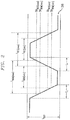
- FIG. 2 shows an illustrative timing diagram of LIN data signal 200 that might be communicated on communication bus 106.
- a LIN data signal 200 has a maximum possible voltage range of V SUP , which is the power supply voltage of devices coupled to the LIN bus.
- V SUP the power supply voltage of devices coupled to the LIN bus.
- a threshold voltage for a receiver to detect a logic high signal has a range between a maximum voltage (TH REC(max) ) and a minimum voltage (TH REC(min) ).
- a threshold for a receiver to detect a logic low signal has a range between a maximum voltage (TH DOM(max) ) and a minimum voltage (TH DOM(min) ). These thresholds must be met by LIN data signal 200 on communication bus 106.
- V SUP is typically slightly less than the voltage of the vehicle battery.
- LIN bus components (and, thus, V SUP ) are typically isolated from the vehicle battery by at least one series diode, having a corresponding voltage drop across it, and by one or more series resistors, each resistor also having a corresponding voltage drop across it that varies in proportion to the current through it.
- the bus voltage might typically be further isolated from V SUP by an additional series diode and pull-up resistor.
- the low range of the bus voltage might also be slightly higher than ground in the case of a voltage drop across a pull-down semiconductor switching element.
- the range of LIN data signal 200 is slightly less than the full range of V SUP .
- LIN data signal 200 has a rise time, t r , and a fall time, t f , that vary based on electrical attributes of devices coupled to communication bus 106 and electrical attributes of communication bus 106 itself, as well as the manner in which LIN data signal 200 is generated.
- FIG. 2 also shows illustrative durations for transmitted bits, where t DOM is the duration of a logic low bit, and t REC is the duration of a logic high bit
- FIG. 2 also shows illustrative rise (t r ) and fall times (t f ) for logic transitions of LIN data signal 200.
- the rise time, t r , and fall time, t f , of LIN data signal 200 should be within the range determined by the maximum and minimum durations for a transmitted bit and maximum rise and fall times as set forth in the LIN specification.
- Changing the rise time, t r , and fall time, t f , of LIN data signal 200 can change an amount of electromagnetic interference (EMI) present on communication bus 106.
- EMI electromagnetic interference
- changes in the characteristics of communication bus 106 for example load resistance and capacitance, can also change the characteristics of LIN data signal 200.
- FIG. 3 shows a block diagram of LIN device 300, which might be employed as one or more of devices 104(1) - 104( N ) of the embodiment shown in FIG. 1 .
- LIN device 300 is coupled to an input voltage V SYS , a ground or circuit common, GND, and communication bus 106, which includes a data signal shown as the signal or node BUS_DATA and, in some embodiments, a ground or circuit common, GND.
- LIN device 300 includes power supply 302 that is coupled to V SYS and GND and generates voltage V SUP that, as described in regard to FIG. 2 , is the power supply voltage of devices coupled to a LIN bus.
- V SUP and GND are provided to various components of LIN device 300, including controller 304, signal conditioning module 306, transmit driver 308 and data source 310.
- V SYS might be substantially equal to V BATT .
- Signal conditioning module 306 is coupled to the BUS_DATA signal of communication bus 106, and might filter, sample, or otherwise condition data received by LIN device 300 on the BUS_DATA signal node. Signal conditioning module 306 provides the conditioned data, as received data signal RX, to controller 304. Controller 304 generally controls the operation of LIN device 300, for example by processing data received from communication bus 106 (e.g., received data RX), and generating data to be transmitted on communication bus 106, which is provided to transmit driver 308 as transmit data signal TX. Transmit driver 308 is coupled to the BUS_DATA signal, and drives the voltage level of the BUS_DATA signal based on transmit data signal TX. Controller 304 might generate transmit data signal TX in response to data provided from data source 310.
- data source 310 might be in communication with one or more devices external to LIN device 300 via communication path 312.
- Communication path 312 might be a wired or wireless connection.
- Data source 310 might be implemented as various sensors or input/output devices.
- LIN device 300 might be a magnetic field sensor and, in such embodiments, data source 310 might include one or more magnetic field sensing elements to detect parameters of a magnetic field, for example in response to the presence or movement of a ferromagnetic or magnetic object.
- magnetic field sensing element is used to describe a variety of electronic elements that can sense a magnetic field for example, but not limited to, a Hall effect element, a magnetoresistance element, or a magnetotransistor.
- magnetic field sensor is used to describe a circuit that uses a magnetic field sensing element, generally in combination with other circuits (e.g., LIN device 300).
- Magnetic field sensors are used in a variety of applications, including, but not limited to, angle sensors that sense an angle of a direction of a magnetic field, a current sensor that senses a magnetic field generated by a current carried by a current-carrying conductor, a magnetic switch that senses the proximity of a ferromagnetic object, a rotation detector that senses passing ferromagnetic articles, for example, magnetic domains of a ring magnet or a ferromagnetic target (e.g., gear teeth) where the magnetic field sensor is used in combination with a back-biased or other magnet, and a linear magnetic field sensor that senses a magnetic field density of a magnetic field.
- angle sensors that sense an angle of a direction of a magnetic field
- a current sensor that senses a magnetic field generated by a current carried by a current-carrying conductor
- a magnetic switch that senses the proximity of a ferromagnetic object
- a rotation detector that senses passing ferromagnetic articles, for example,
- Described embodiments might desirably operate communication bus 106 as a LIN bus in an open-loop mode.
- some embodiments of transmit driver 308 employ a current mirror circuit to generate a shaped current waveform to charge and discharge communication bus 106 in an open-loop operation mode.
- the current mirror circuit employs bipolar junction transistors (BJTs)
- the current waveform that charges and discharges the LIN bus e.g., the BUS_DATA signal
- the current waveform that charges and discharges the LIN bus is exponential versus time (e.g., the current through the transistor (e.g., the collector-emitter current) is related exponentially to the base-emitter voltage of the transistor (e.g., V BE )).
- the current waveform that charges and discharges the LIN bus (e.g., the BUS_DATA signal) follows a square-law relationship (e.g., the current through the transistor (e.g., the drain-source current) is related to the gate-source voltage-squared (e.g., V GS 2 )).
- MOSFETs metal oxide semiconductor field effect transistors
- the current mirror circuit employs MOSFETs (e.g., current related to gate-source voltage squared) or BJTs (e.g., current exponentially related to base-emitter voltage)
- MOSFETs current related to gate-source voltage squared
- BJTs current exponentially related to base-emitter voltage
- the current sunk from communication bus 106 starts as a small current and gradually increases before increasing rapidly (e.g., increases exponentially in the case of BJTs used in the current mirror, or increases based on the square-law for MOSFETs).
- the BUS_DATA voltage will decrease more quickly than if communication bus 106 has higher resistance or higher load capacitance.
- communication bus 106 has low resistance and/or low load capacitance, most of the bus discharging occurs during the linear region of the current waveform (e.g., very quickly).
- communication bus 106 has high resistance and/or high load capacitance, the voltage will decrease less quickly and thus most of the bus discharging occurs during the non-linear part of the current waveform. This is preferable to a single-value or linearly ramped current as the timings (e.g., the rise and fall times and, thus, the bit duty cycles), can be more accurately controlled over variances in load conditions without generating increased EMI.
- the current draw through the current mirror circuit is turned off.
- the current mirror circuit employs MOSFETs (e.g., current related to gate-source voltage squared) or BJTs (e.g., current exponentially related to base-emitter voltage)
- MOSFETs current related to gate-source voltage squared
- BJTs current exponentially related to base-emitter voltage
- the BUS_DATA signal is driven from low-to-high, the current sunk from communication bus 106 starts as a large current and decreases rapidly before decreasing more gradually (e.g., decreases exponentially in the case of BJTs used in the current mirror, or decreases based on the square-law for MOSFETs).
- the BUS_DATA voltage will increase more quickly than if communication bus 106 has higher resistance or higher load capacitance.
- FIG. 4 is a schematic of an illustrative embodiment of transmit driver 308. As shown in FIG. 4 , transmit driver 308 is coupled to the BUS_DATA signal of communication bus 106. The BUS_DATA signal is coupled to an input node of transistor Q1 and the cathode of diode D.
- the terms “input node” and “output node” refer generically to either the source or drain of a metal-oxide semiconductor (MOS) field effect transistor (also referred to as a MOSFET) or the emitter or collector of a bi-polar junction transistor (also referred to as a BJT), and the term “control node” refers generically to the gate of the MOSFET or the base of the BJT.
- MOS metal-oxide semiconductor
- BJT bi-polar junction transistor
- Diode D is coupled in series between supply voltage V SUP and resistor R, with the anode of diode D coupled to V SUP and the cathode of diode D coupled to resistor R.
- a control node of transistor Q1 is coupled to Node 1.
- An output node (e.g., the source) of transistor Q1 is coupled to GND.
- the anode of diode D2 is coupled to BUS DATA, and the cathode of diode D2 is coupled to an output node (e.g., the drain) of transistor Q1.
- resistor R and diode D operate to charge or pull-up the BUS_DATA signal to approximately the voltage of V SUP (e.g., V SUP less the voltage drop across resistor R and diode D).
- diode D2 and transistor Q1 operate, in response to the signal at Node 1, to controllably discharge or pull-down the BUS_DATA signal to approximately the voltage of GND (e.g., GND plus the voltage across transistor Q1, e.g., the drain-to-source voltage, V DS , in embodiments where Q1 is a metal-oxide semiconductor field effect transistor (MOSFET), such as shown in FIG. 4 ).
- MOSFET metal-oxide semiconductor field effect transistor
- the voltage of Node 1 and, thus, the voltage of the control node of transistor Q1, is controlled by current sources I1 and I2 and switches SWa and SWb.
- Switches SWa and SWb operate in response to transmit data signal TX.
- switch SWa is closed (e.g., on) when transmit data signal TX is logic low and open (e.g., off) when TX is logic high (e.g., the logic of SWa is the inverse of TX, shown as TX ).
- Switch SWb is closed (e.g., on) when transmit data signal TX is logic high and open (e.g., off) when TX is logic low (e.g., the logic of SWb is the same as the logic of TX).
- transistor Q1 is an NFET (as shown in FIG. 4 ) or an N-type BJT (not shown)
- discharging the control node of transistor Q1 results in decreasing the current flowing through transistor Q1, shown as current 13.
- current I3 approaches zero
- transistor Q1 is turned “off”
- the BUS_DATA signal charges from V SUP through resistor R and diode D. Therefore, turning off transistor Q1 allows transmit driver 308 to transmit a logic high on the BUS_DATA signal of communication bus 106.
- Controlling the rate at which transistor Q1 is turned off by controlling the speed at which Node 1 is discharged allows control of how fast the BUS_DATA signal can charge (e.g., by controlling I3).
- current I3 is related to Ql's gate-source voltage squared.
- transistor Q1 when transistor Q1 is an NFET (as shown in FIG. 4 ) or an N-type BJT, charging the control node of transistor Q1 results in increasing the current flowing through transistor Q1, current 13. As Node 1 is increasingly charged, current I3 increases, and transistor Q1 is "on". When transistor Q1 is on, the BUS_DATA signal discharges through transistor Q1, and therefore, turning on transistor Q1 allows transmit driver 308 to transmit a logic low on the BUS_DATA signal of communication bus 106. Controlling the rate at which transistor Q1 is turned on by controlling the speed at which Node 1 is charged (e.g., by controlling I1) allows control of how fast the BUS_DATA signal can discharge (e.g., by controlling 13). As described above, when Q1 is a BJT, current 13 is related exponentially to Q1's base-emitter voltage.
- switches SWa and SWb could be reversed if transistor Q1 were implemented as a PFET or P-type BJT. Further, switches SWa and SWb could be implemented as mechanical switches or as one or more transistors or other semiconductor switching elements (e.g., triacs, thyristors, silicon controlled rectifiers (SCRs), etc.).
- switches SWa and SWb could be implemented as mechanical switches or as one or more transistors or other semiconductor switching elements (e.g., triacs, thyristors, silicon controlled rectifiers (SCRs), etc.).
- transmit driver 308 can beneficially control the bit durations (e.g., t DOM and t REC ), rise time, t r , and fall time, t f , of the BUS_DATA signal, as well reduce the amount of EMI that is generated by LIN device 300 and coupled to communication bus 106. Further, embodiments employing components that exhibit both linear and non-linear properties (e.g., transistors) allow for increased control of the rate of charge and discharge of the BUS_DATA signal, as will be described in greater detail below.
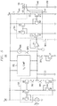
- FIG. 5 shows additional detail of transmit driver 308.
- transmit driver 308 might desirably employ an actively driven current mirror circuit to charge and discharge the BUS_DATA signal.
- current mirror circuit 504 is formed by transistors Q8, Q9, Q10 and Q11.
- Transistors Q8 and Q9, and transistors Q10 and Q11 form current mirror pairs of current mirror circuit 504.
- transistors Q8 and Q9 are P-channel FETs and transistors Q2, Q10 and Q11 are N-channel FETs.
- transistors Q8 and Q9 might be N-channel FETs and transistors Q2, Q10 and Q11 might be P-channel FETs.
- transistors Q2, Q8, Q9, Q10 and Q11 might be BJTs.
- FIG. 5 only the embodiment shown in FIG. 5 will be described herein, although one of skill in the art will appreciate how to implement transistors Q2, Q8, Q9, Q10 and Q11 as different types of transistors or as transistors having different doping.
- Current mirror circuit 504 is actively driven by operational amplifier (op amp) OP1.
- the non-inverting input of op amp OP1 is designated as Node 1, and the output of op amp OP1 is designated as Node 2.
- the output of op amp OP1 (e.g., Node 2) is fed back to the inverting input of op amp OP1.
- Node 2 is also coupled to switch SW1c, which is coupled between Node 2 and ground.
- Node 2 provides the control input to current mirror circuit 504 by being coupled to the control node of transistor Q2 (e.g., the gate of MOSFET Q2).
- the drain of transistor Q2 is coupled to the drain of transistor Q8.
- the source of transistor Q2 is coupled to ground.
- the output of current mirror 504 is the BUS_DATA signal coupled to communication bus 106.
- the input nodes of transistors Q8 and Q9 are coupled to V SUP (e.g., the source nodes of the P-channel FETs are coupled to V SUP ).
- V SUP e.g., the source nodes of the P-channel FETs are coupled to V SUP .
- the gates of transistors Q8 and Q9 are coupled to each other and also coupled to a node between transistors Q8 and Q2 (e.g., the drain of transistor Q8 and the drain of transistor Q2).
- the drain of transistor Q10 is coupled to the drain of transistor Q9.
- the gates of transistors Q10 and Q11 are coupled to each other and also coupled to a node between transistors Q9 and Q10 (e.g., the drain of transistor Q9 and the drain of transistor Q10).
- the drain of transistor Q11 is coupled to the BUS_DATA signal and to V SUP through resistor R LOAD .
- the source of transistor Q11 is coupled to ground.
- the BUS_DATA signal is also coupled to load capacitance C LOAD .
- a diode might be in series with R LOAD (e.g., diode D shown in FIG. 4 ).
- a diode might be placed in series with transistor Q11 (e.g., with the anode coupled to BUS_DATA and the cathode coupled to the drain of Q11, shown as diode D2 in FIGs. 4 and 5 ).
- the current through transistor Q2 controls the current through transistor Q9, which in turn controls the current through transistor Q11.
- the current through transistor Q11 might be a multiple of the current through transistor Q2.
- the current through transistor Q11, I OUT determines the rate of charge or discharge of the BUS_DATA signal.
- Transistor Q2 is driven by op amp OP1 (e.g., by controlling Node 2).
- op amp OP1 e.g., by controlling Node 2
- the operation of op amp OP1 is controlled based on the operation of V GS clamp circuit 502, capacitor C1, transistors Q3, Q4, Q5, Q6 and Q7, and switches SW2, SW4, SW1A, and SW1B (e.g., by controlling Node 1).
- Node 1 is coupled to current source I START via switch SW1B, and also coupled to transistor Q1 via switch SW1A.
- Capacitor C1 is coupled between ground and Node 1 to control charge and discharge of Node 1.
- Node 1 is also coupled to the drains of transistors Q5 and Q7 via switches SW2 and SW4, respectively.
- Current mirror circuit 506 includes transistors Q3, Q4, Q5, Q6 and Q7.
- Transistor Q3 is coupled, source-to-drain, between V SUP and current V GS R .
- the control node of transistor Q3 is coupled to the drain of Q3, and to the control nodes of transistors Q4 and Q5.
- the control node of transistors Q3, Q4 and Q5 might be coupled to controller 304 ( FIG. 3 ), for example to enable transmit driver 308 to drive the BUS_DATA signal in response to transmit data (e.g., transmit data signal TX).
- Transistor Q4 is coupled, source-to-drain, between V SUP and the drain and control node of transistor Q6.
- the source of transistor Q6 is coupled to ground.
- the control node of transistor Q6 is also coupled to the control node of transistor Q7.
- the source of transistor Q7 is coupled to ground.
- the source of transistor Q5 is coupled to VSUP, and the drain of transistor Q5 is coupled to switch SW2, which selectively couples the drain of transistor Q5 to Node 1.
- the drain of transistor Q7 is coupled to switch SW4, which selectively couples the drain of transistor Q7 to Node 1.
- transistors Q3, Q4, Q5, Q6 and Q7 collectively form current mirror circuit 506, which drives op amp OP1 (e.g., Node 1) and, in turn, drives current mirror 504 to charge and discharge capacitor C1 and, in turn, the BUS_DATA signal to transmit data on communication bus 106.
- V GS clamp circuit 502 might include a first current source, I LIM , and a second current source, V SUP R ⁇ ⁇ .
- the current sources are coupled to V SUP and transistor Q a via switches SW3A and SW3B, respectively.
- switches SW3A and SW3B operate in response to control signal ⁇ .
- switch SW3A is closed (e.g., on) when control signal ⁇ is logic low and open (e.g., off) when control signal ⁇ is logic high (e.g., the logic of SW3A is the inverse of control signal ⁇ , shown as ( ⁇ )).
- Switch SW3B is closed (e.g., on) when control signal ⁇ is logic high and open (e.g., off) when control signal ⁇ is logic low (e.g., the logic of SW3B is the same as the logic of control signal ⁇ ).
- V GS clamp circuit 502 also includes transistors Q b and Q c .
- Transistor Q b is coupled, drain-to-source, between V SUP and ground through switch SW1A.
- Transistor Q c is coupled, drain-to-source, between Node 1 and ground through switch SW1A.
- Switch SW1A operates in response to control signal ⁇
- the control node of transistor Q b is coupled to the control node of transistor Q a , which is coupled to an input node of transistor Q d .
- the control node of transistor Q c is coupled to Node 1.
- control signal ⁇ when control signal ⁇ is logic high, switch SW3A is open and SW3B is closed, thus connecting current source V SUP R ⁇ ⁇ to transistor Q a , which is coupled, through transistor Q d , to Node 1.
- Transistor Q d is controlled by control signal ⁇ , such that when control signal ⁇ is logic high, transistor Q d is on, and when control signal ⁇ is logic low, transistor Q d is off.
- control signal ⁇ is logic high
- Node 1 is charged by current source V SUP R ⁇ ⁇ , which current is fed in transistor Q a , which clamps Node 1 to the same voltage as the V GS voltage of transistor Q a .
- switch SW3A when control signal ⁇ is logic low, switch SW3A is closed and SW3B is open, thus connecting current source I LIM to transistor Q a .
- Transistor Q d is off when control signal ⁇ is logic low.
- I LIM is coupled to the gate of transistors Q a and Q b .
- switch SW1A When control signal ⁇ is logic low, switch SW1A is closed, and Node 1 is discharged by the current through transistor Q c if the voltage on node 1 rises higher than the V GS voltage of transistor Q a .
- the current through transistor Q b is based on current I LIM
- the current through transistor Q c is based on the voltage of Node 1 (e.g., varies as the voltage of Node 1 varies, such that when Node 1 is charged to a higher voltage level, the current through transistor Q c is high, and as Node 1 discharges, the current through transistor Q c decreases).
- the maximum current through transistors Q b and Q c is limited to the current through SW1A.
- transistor Q c clamps the voltage of Node 1 and limits the output current (e.g., I OUT ).
- the current through transistor Q c is limited by current I SW1A (shown as transistor Q1 in FIG. 5 ). In some embodiments, current I SW1A is slightly larger than the current V GS R (shown in FIG. 5 ).
- V GS clamp circuit 502 provides a constant maximum current limit (e.g., I LIM ). Further, V GS clamp circuit 502 provides current source V SUP R ⁇ ⁇ that clamps the voltage of Node 1 to the gate-to-source voltage, V GS , of transistor Q a . Thus, current V SUP R ⁇ ⁇ might prevent an overcurrent condition at I OUT (e.g., by clamping the voltage of Node 1). Transmit driver 308 provides current V GS R to linearly charge and discharge Node 1, which in turn charges and discharges Node 2. As shown in FIG.
- Node 1 when Node 1 is discharged (e.g., a logic low), Node 2 is a logic low, which means that the BUS_DATA signal is charged (e.g., a logic high).
- the BUS_DATA signal is discharged (e.g., a logic low).
- V GS clamp circuit 502 limits the maximum output current (e.g., I OUT ) based on current I LIM , and clamps the voltage of Node 1 in preparation of charging the BUS_DATA signal based on current V SUP R ⁇ ⁇ .
- transistors Q1 and Q2 are matched to the transistors of V GS clamp circuit 502 that generate current V SUP R ⁇ ⁇ (e.g., transistors Q a , Q b and Q c of FIG. 6 ) and also matched to the transistors that generate current V GS R .
- a pre-charge voltage, V MIN , of Node 1 is set by current I START being fed to Node 1.
- Current I START is a small current that pre-charges Node 1 such that the output current, I OUT , present on the BUS_DATA node can be increased quickly but without having a sudden or sharp edge or spike, which could increase EMI.
- I START might be approximately 1 ⁇ A.
- a maximum voltage, V MAX , of Node 1 is set by V GS clamp circuit 502 that clamps Node 1 to a voltage equal to the voltage produced from the current fed into transistor Q a , which, in turn, sets the clamp voltage via transistors Q b and Q c .
- Node 1 varies over the range of V MIN to V MAX and the current to Node 1 varies between 0, I START , V SUP R ⁇ ⁇ and I LIM .
- V GS clamp circuit 502 is changed to a scaled current related to V SUP /R LOAD , shown in FIG. 6 as current V SUP R ⁇ ⁇ , with a minimum value of R LOAD selected. If a maximum value of R LOAD is chosen and the actual load resistance is less, a voltage step would result which is undesirable, for example for EMI.
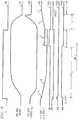
- FIGs. 7 and 8 illustrate the relationship between the signals described in regard to FIGs. 5 and 6 over an elapsed time, t.
- FIG. 7 shows the signals over a time, t, that includes multiple transitions (e.g., multiple cycles) of transmit data signal TX.
- FIG. 8 shows the signals over a time, t, that includes a single cycle (e.g., one low-to-high transition and one high-to-low transition) of transmit data signal TX.
- curve 702 illustrates transmit data signal TX
- curve 704 illustrates the voltage of the BUS_DATA signal
- curve 706 represents the current (e.g., current I OUT of FIG. 5 ) of the BUS_DATA signal (e.g., the current flowing into and out of LIN device 300 at the BUS_DATA node)
- curve 708 represents the voltage on Node 1 (hashed line) and the voltage on Node 2 (solid line)
- curves 710(1), 710(2), 710(3) and 710(4) represent the logic state (e.g., logic high is "on” or closed, and logic low is “off” or open) of switches SW1 (which includes switches SW1A, SW1B and SW1C), SW2, SW3 (which includes switches SW3A and SW3B shown in FIG. 6 ) and SW4, respectively.
- activity periods A, B, C, D and E correspond to five distinct activity periods on Node 1 in response to transmit data signal TX, shown in FIGs. 7 and 8 as activity periods A, B, C, D and E.
- activity periods A and B correspond to low-to-high transitions of transmit data signal TX (e.g., the BUS_DATA signal).
- Activity period C occurs before, and in preparation of, a high-to-low transition of transmit data signal TX.
- Activity periods D and E correspond to high-to-low transitions of transmit data signal TX (e.g., the BUS DATA signal).
- the voltage of Node 1 is set to a predetermined level by a pre-charge current feeding transistor Q a . More particularly, for a very short time, shown in FIG. 8 as time T A , in response to transmit data signal TX going high, Node 1 and Node 2 are set to a voltage equal to V GS by a current V SUP R ⁇ ⁇ by VGS clamp circuit 502 (e.g., switch SW3B is closed). This pre-charges Node 1 and Node 2, thus starting to turn off transistor Q11 and reducing the pull-down current I OUT .
- Reducing the pull-down current I OUT allows the BUS_DATA signal to start to charge up soon after transmit data signal TX goes high, minimizing delay in the response of the BUS_DATA signal. Further, gradually reducing the pull-down current I OUT , allows the BUS_DATA signal to charge without causing EMI, such as might be caused by suddenly reducing the pull-down current I OUT to zero.
- FIG. 9 shows a flow diagram of operation technique 900 employed by LIN device 300.
- a transceiver of LIN device 300 starts to operate.
- the transceiver might include transmit driver 308 and signal conditioning module 306, both of which are coupled to controller 304.
- one or more transceiver attributes might optionally be calibrated based on, for example, estimated channel characteristics of communication bus 106.
- received signals might be corrupted by frequency-dependent signal loss of the channel, inter-symbol interference (ISI), EMI and other noise, such as crosstalk, echo, signal dispersion and distortion.
- ISI inter-symbol interference
- EMI EMI and other noise, such as crosstalk, echo, signal dispersion and distortion.
- receivers might equalize the channel to compensate for such distortions. Equalization might be performed by one or more equalizers or filters, such as a decision-feedback equalizer (DFE) and a continuous time analog equalizer (AEQ), which might be employed to remove inter-symbol interference and other noise.
- DFE decision-feedback equalizer
- AEQ continuous time analog equalizer
- Equalizer parameters that can be adapted might include, for example, a number of active filter taps, weight coefficients of each active filter tap, variable component values to set filter characteristics such as frequency response or an order of the filter, values of components of a matching network, etc.
- channel characteristics might be estimated based upon one or more calibration signals received by signal conditioning module 306 from communication bus 106.
- a predetermined (e.g., known) calibration signal might be provided over communication bus 106. Comparing the received data to the known calibration data, controller 304 might optionally adjust one or more settings of signal conditioning module 306 to improve the quality of the received data.
- settings of transmit driver 308 might be adjusted to calibrate, for example, the charge and discharge time of the BUS DATA signal of transmit driver 308.
- LIN device 300 operates in a receive mode (e.g., transmit driver 308 is not transmitting data on the BUS_DATA signal, and signal conditioning module 306 waits to receive data on the BUS_DATA signal). Signal conditioning module 306 processes any data received on the BUS_DATA signal, and provides the processed received data to controller 304.
- controller 304 has data to transmit
- LIN device 300 is operated in transmit mode. Otherwise, if there is no data to transmit at block 910, technique 900 returns to block 908, where LIN device 300 operates in receive mode.
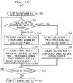
- FIG. 10 shows additional detail of transmit mode block 912 of FIG. 9 .
- transmit mode 912 begins, for example when controller 304 determines there is data to send on communication bus 106.
- transmit driver 308 asserts high or low signal levels on the BUS_DATA signal.
- transmit driver 308 needs to transition the BUS_DATA signal from low-to-high, then processing continues to block 1006.
- the voltage (or bias level) of Node 1 is set to a predetermined initial bias level (corresponding to activity period A shown in FIGs. 7 and 8 ).
- the voltage of Node 1 is set to a predetermined level by a pre-charge current. More particularly, for a very short time, shown in FIG. 8 as time T A , in response to transmit data signal TX going high, Node 1 and Node 2 are set to a reduced voltage equal to V GS by a current V SUP R ⁇ ⁇ by VGS clamp circuit 502 (e.g., switch SW3B is closed).
- the voltage (or bias level) of Node 1 is linearly reduced to a minimum voltage level over time period T B corresponding to activity period B shown in FIGs. 7 and 8 .
- Node 1 is discharged by a current based on current V GS R .
- time period T B might be set based upon the value of R LOAD .
- time period T B might be set based upon one or more determined characteristics of communication bus 106 (e.g., at optional step 904 shown in FIG. 9 ).
- Node 1 is linearly discharged by current V GS R . Due to the square-law (MOSFET) or exponential (BJT) relationship of the currents of transistor Q2 that is mirrored in the current mirror circuit, the BUS_DATA signal is non-linearly charged as the BUS_DATA discharge current (e.g., I OUT ) is reduced during activity period B. The current through transistor Q11 (e.g., I OUT ) is non-linearly reduced, thus allowing charging of BUS_DATA through the R-C network including R LOAD and C LOAD .
- MOSFET square-law
- BJT exponential
- the voltage of BUS_DATA reaches a maximum voltage (e.g., approximately V SUP ) as the BUS_DATA discharge current I OUT reaches, and is maintained at, zero.
- a maximum voltage e.g., approximately V SUP
- I OUT current discharge current
- Node 1 is "pre-charged" (e.g., charged prior to a low-to-high transition in transmit data signal TX) to a start voltage such that a sudden edge of BUS_DATA does not occur but there is also not a delay in discharging the BUS_DATA signal.
- switch SW1B is closed at block 1010 to pre-charge Node 1 by current I START (e.g., a predetermined minimum start current to set a predetermined minimum pre-charge bias level of Node 1 into a gate-drain connected FET, e.g., transistor Q1).
- I START e.g., a predetermined minimum start current to set a predetermined minimum pre-charge bias level of Node 1 into a gate-drain connected FET, e.g., transistor Q1).
- the pre-charging occurs for a time, T C , corresponding with activity period C shown in FIGs. 7 and 8 .
- T C the internal nodes of the output power stage (e.g., circuit 506 and op amp OP1) are pre-charged in order to minimize delay in the output waveform upon the high-to-low transition of transmit data signal TX.
- Node 2 remains low (e.g., off) even while Node 1 is pre-charged, for example due to switch SW1C being closed until transmit data signal TX goes low.
- switch SW1C is opened, and Node 2 jumps to the precharge level of Node 1, allowing current I OUT to be increased quickly but without jumping to a large current draw for I OUT , and, thus allowing the BUS_DATA voltage to start decreasing quickly but having a rounded edge to prevent EMI.
- time period T D During activity period D, lasting for time T D , Node 1 and Node 2 charge linearly to a maximum voltage level over time period T D .
- the charge current might be a scaled version of current V GS R shown in FIG. 5 .
- time period T D might be set based upon the value of R LOAD .
- time period T D might be set based upon one or more determined characteristics of communication bus 106 (e.g., at optional step 904 shown in FIG. 9 ). Due to the square-law (MOSFET) or exponential
- the BUS_DATA signal is non-linearly discharged as the BUS_DATA discharge current (e.g., I OUT ) is increased during activity period D.
- the voltage of BUS_DATA reaches a minimum voltage (e.g., approximately GND or circuit common) as the BUS_DATA discharge current I OUT reaches, and is maintained at, a maximum current (as indicated by activity period E).
- a variable discharging rate of the BUS_DATA signal is provided during activity periods C and D.
- V GS clamp circuit 502 acts as a current limit, limiting the voltage on Node 1 based on current I LIM . After block 1012, processing continues to block 1014.
- controller 304 if controller 304 has additional data to transmit, then processing returns to block 1004 to transmit one or more subsequent bits on communication bus 106. If, at block 1014, controller 304 does not have additional data to transmit, then processing continues to block 1012, where transmit mode 912 is completed.
- described embodiments provide improved timing of the rising and falling edges of the output signal, BUS_DATA, thus requiring little, if any, trimming.
- the error due to the accuracy of the absolute current adds to total error, which is reduced and, ideally, eliminated by the variable current generated in described embodiments.
- the rise and fall times of the BUS_DATA voltage can be more precisely controlled than if a linear current controls the voltage of BUS_DATA.
- described embodiments set output current I OUT initially at a low value and ramp I OUT slowly to the exponential part of the waveform over time. This gives more of a rounding effect to the down-going edge of the BUS_DATA voltage waveform, reducing EMI.
- the I OUT current starts at a precharge current level, I START , reducing timing delays due to starting in the non-linear part of the current curve.
- This pre-charging eliminates any need for feedback on the BUS_DATA node. Eliminating feedback and, thus, an additional signal connection to the BUS_DATA signal, might also reduce EMI, by reducing the potential to generate EMI onto the BUS_DATA signal, and also by reducing the likelihood of EMI present on the BUS_DATA signal from being coupled into LIN device 300.
- any variances in load parasitic components e.g., load resistance, inductance or capacitance
- load resistance, inductance or capacitance has reduced effect in terms of rise and fall times of the BUS_DATA signal when compared to a constant or linearly ramped current.
- less EMI is generated while also maintaining rise and fall times across different load conditions.
- described embodiments employ open-loop control (e.g., the BUS_DATA signal is not fed back internally to controller 304).
- open-loop control e.g., the BUS_DATA signal is not fed back internally to controller 304.
- Node 1 For low-to-high transitions of the BUS_DATA signal, Node 1 is pro-charged to a matched V GS fed with V SUP /R.
- Node 1 For high-to-low transitions of the BUS_DATA signal, Node 1 is clamped to a matched V GS fed with a small current (e.g., I START ) so that internal nodes can bias quickly, but not so large that the output experiences a "jump" or "glitch".
- I START small current
- the words “exemplary” and “illustrative” are used herein to mean serving as an example, instance, or illustration. Any aspect or design described herein as “exemplary” or “illustrative” is not necessarily to be construed as preferred or advantageous over other aspects or designs. Rather, use of the words “exemplary” and “illustrative” is intended to present concepts in a concrete fashion.
- system generally intended to refer to a computer-related entity, either hardware, a combination of hardware and software, software, or software in execution.
- a component might be, but is not limited to being, a process running on a processor, a processor, an object, an executable, a thread of execution, a program, and/or a computer.
- an application running on a controller and the controller can be a component.
- One or more components might reside within a process and/or thread of execution and a component might be localized on one computer and/or distributed between two or more computers.
- circuits While the exemplary embodiments have been described with respect to processes of circuits, described embodiments might be implemented as a single integrated circuit, a multi-chip module, a single card, or a multi-card circuit pack. As would be apparent to one skilled in the art, various functions of circuit elements might also be implemented as processing blocks in a software program. Such software might be employed in, for example, a digital signal processor, micro-controller, or general purpose computer.
- Some embodiments might be implemented in the form of methods and apparatuses for practicing those methods. Described embodiments might also be implemented in the form of program code embodied in tangible media, such as magnetic recording media, hard drives, floppy diskettes, magnetic tape media, optical recording media, compact discs (CDs), digital versatile discs (DVDs), solid state memory, hybrid magnetic and solid state memory, or any other machine-readable storage medium, wherein, when the program code is loaded into and executed by a machine, such as a computer, the machine becomes an apparatus for practicing the claimed invention.
- tangible media such as magnetic recording media, hard drives, floppy diskettes, magnetic tape media, optical recording media, compact discs (CDs), digital versatile discs (DVDs), solid state memory, hybrid magnetic and solid state memory, or any other machine-readable storage medium, wherein, when the program code is loaded into and executed by a machine, such as a computer, the machine becomes an apparatus for practicing the claimed invention.
- Described embodiments might also be implemented in the form of program code, for example, whether stored in a storage medium, loaded into and/or executed by a machine, or transmitted over some transmission medium or carrier, such as over electrical wiring or cabling, through fiber optics, or via electromagnetic radiation, wherein, when the program code is loaded into and executed by a machine, such as a computer, the machine becomes an apparatus for practicing the claimed invention.
- program code segments When implemented on a processing device, the program code segments combine with the processor to provide a unique device that operates analogously to specific logic circuits.
- Such processing devices might include, for example, a general purpose microprocessor, a digital signal processor (DSP), a reduced instruction set computer (RISC), a complex instruction set computer (CISC), an application specific integrated circuit (ASIC), a field programmable gate array (FPGA), a programmable logic array (PLA), a microcontroller, an embedded controller, a multi-core processor, and/or others, including combinations of the above.
- DSP digital signal processor
- RISC reduced instruction set computer
- CISC complex instruction set computer
- ASIC application specific integrated circuit
- FPGA field programmable gate array
- PDA programmable logic array
- microcontroller an embedded controller
- multi-core processor a multi-core processor
- Couple refers to any manner known in the art or later developed in which energy is allowed to be transferred between two or more elements, and the interposition of one or more additional elements is contemplated, although not required.
- the terms “directly coupled,” “directly connected,” etc. imply the absence of such additional elements.
- Signals and corresponding nodes or ports may be referred to by the same name and are interchangeable for purposes here.
- the term "compatible" means that the element communicates with other elements in a manner wholly or partially specified by the standard, and would be recognized by other elements as sufficiently capable of communicating with the other elements in the manner specified by the standard.
- the compatible element does not need to operate internally in a manner specified by the standard.
- all gates are powered from a fixed-voltage power domain (or domains) and ground unless shown otherwise. Accordingly, all digital signals generally have voltages that range from approximately ground potential to that of one of the power domains and transition (slew) quickly. However, and unless stated otherwise, ground may be considered a power source having a voltage of approximately zero volts, and a power source having any desired voltage might be substituted for ground. Therefore, all gates might be powered by at least two power sources, with the attendant digital signals therefrom having voltages that range between the approximate voltages of the power sources.
- Transistors are typically shown as single devices for illustrative purposes. However, it is understood that transistors will have various sizes and characteristics and might be implemented as multiple transistors coupled in parallel to achieve desired electrical characteristics from the combination, such as a desired physical size (e.g., gate width and length) or operating characteristic (e.g., isolation, switching speed, threshold voltage, gain, etc.). Further, the illustrated transistors might be composite transistors.
- a desired physical size e.g., gate width and length
- operating characteristic e.g., isolation, switching speed, threshold voltage, gain, etc.
- the illustrated transistors might be composite transistors.
- each numerical value and range should be interpreted as being approximate as if the word “about”, “substantially” or “approximately” preceded the value of the value or range.
Landscapes
- Engineering & Computer Science (AREA)
- Theoretical Computer Science (AREA)
- General Engineering & Computer Science (AREA)
- Physics & Mathematics (AREA)
- General Physics & Mathematics (AREA)
- Computer Hardware Design (AREA)
- Computing Systems (AREA)
- Signal Processing (AREA)
- Computer Networks & Wireless Communication (AREA)
- Mathematical Physics (AREA)
- Nonlinear Science (AREA)
- Dc Digital Transmission (AREA)
- Electronic Switches (AREA)
Claims (20)
- Sender, Folgendes umfassend:eine Steuerung (304), die konfiguriert ist, um Daten zum Senden durch den Sender über einen mit dem Sender gekoppelten seriellen Bus (106) zu erzeugen; undeinen Sendetreiber (308), der mit der Steuerung gekoppelt ist und einen Ausgangstransistor mit einem Ausgangsknoten umfasst, der mit dem seriellen Bus gekoppelt ist, wobei der Sendetreiber ferner wenigstens einen Stromspiegelkreis (504, 506) umfasst und zu Folgendem, als Reaktion auf die zum Senden erzeugten Daten, konfiguriert ist:Erzeugen von Low-bis-High-Logikübergängen auf dem seriellen Bus durch (i) Festlegen eines Vorspannungspegels des Ausgangstransistors auf einen vorbestimmten anfänglichen Vorspannungspegel durch einen ersten Vorspannungsstrom, wodurch ein Busstrom erzeugt wird, um den seriellen Bus für eine erste Zeitdauer aufzuladen, und (ii) lineares Ändern des Vorspannungspegels von dem vorbestimmten anfänglichen Vorspannungspegel zu einem zweiten Vorspannungspegel durch einen vorbestimmten zweiten Vorspannungsstrom, wodurch ein Busstrom erzeugt wird, um den seriellen Bus für eine zweite Zeitdauer aufzuladen, wodurch der Ausgangstransistor konfiguriert ist, um den Ausgangsknoten nicht linear aufzuladen; undErzeugen von High-bis-Low-Logikübergängen auf dem seriellen Bus durch (i) Vorladen des Vorspannungspegels des Ausgangstransistors auf einen vorgeladenen Vorspannungspegel durch einen vorgeladenen Vorspannungsstrom, wodurch ein Busstrom erzeugt wird, um den seriellen Bus zu entladen, und (ii) lineares Ändern des Vorspannungspegels von dem vorgeladenen Vorspannungspegel zu einem vierten Vorspannungspegel, wodurch ein Busstrom erzeugt wird, um den seriellen Bus für eine dritte Zeitdauer zu entladen, wodurch der Ausgangstransistor konfiguriert ist, um den Ausgangsknoten nicht linear zu entladen,wobei der Sendetreiber einen Klemmstromkreis (502) umfasst, der konfiguriert ist, um eine konstante maximale Stromgrenze bereitzustellen, um einen Überstromzustand des Busstroms zu verhindern,dadurch gekennzeichnet, dass die Steuerung konfiguriert ist, um den Sender zu kalibrieren,wobei die Steuerung für die Kalibrierung zu Folgendem konfiguriert ist:Schätzen einer oder mehrerer störender Komponenten des seriellen Busses; undFestlegen des vorbestimmten anfänglichen Vorspannungspegels, des zweiten Vorspannungspegels, des vorgeladenen Vorspannungspegels, des maximalen Vorspannungspegels, des minimalen Vorspannungspegels, der ersten vorbestimmten Zeitdauer und/oder der zweiten vorbestimmten Zeitdauer basierend, wenigstens teilweise, auf der geschätzten einen oder den mehreren störenden Komponenten des seriellen Busses.
- Sender nach Anspruch 1, wobei der Ausgangstransistor einen Metall-Oxid-Halbleiter-Feldeffekttransistor (metal-oxide semiconductor field effect transistor - MOSFET) umfasst.
- Sender nach Anspruch 2, wobei:der Ausgangstransistor einen N-Kanal-MOSFET umfasst;wobei der N-Kanal-MOSFET konfiguriert ist, um Low-bis-High-Logikübergänge auf dem seriellen Bus zu erzeugen, wenn die Steuerung zu Folgendem konfiguriert ist: (i) Festlegen des Vorspannungspegels eines Steueranschlusses des Ausgangstransistors auf den vorbestimmten anfänglichen Vorspannungspegel, und (ii) lineares Entladen des Steueranschlusses von dem vorbestimmten anfänglichen Vorspannungspegel auf den zweiten Vorspannungspegel, wobei der zweite Vorspannungspegel ein minimaler Vorspannungsschwellenwert des MOSFET ist;wobei der N-Kanal-MOSFET konfiguriert ist, um High-bis-Low-Logikübergänge auf dem seriellen Bus zu erzeugen, wenn die Steuerung zu Folgendem konfiguriert ist: (i) Vorladen des Steueranschlusses des Ausgangstransistors auf den vorgeladenen Vorspannungspegel durch einen vorgeladenen Vorspannungsstrom, und (ii) lineares Aufladen des Steueranschlusses von dem vorgeladenen Vorspannungspegel auf den vierten Vorspannungspegel, wobei der vierte Vorspannungspegel ein maximaler Vorspannungsschwellenwert des MOSFET ist; undwobei der Ausgangsknoten nicht linear aufgeladen und entladen wird, indem ein Drain-Source-Strom durch den MOSFET gemäß einem Quadratwert des Vorspannungspegels geändert wird.
- Sender nach Anspruch 2, wobei:der Ausgangstransistor einen P-Kanal-MOSFET umfasst;wobei der P-Kanal-MOSFET konfiguriert ist, um Low-bis-High-Logikübergänge auf dem seriellen Bus zu erzeugen, wenn die Steuerung zu Folgendem konfiguriert ist: (i) Vorladen eines Steueranschlusses des Ausgangstransistors auf einen voraufgeladenen Vorspannungspegel durch einen vorgeladenen Vorspannungsstrom, und (ii) lineares Aufladen des Steueranschlusses von dem vorgeladenen Vorspannungspegel auf einen maximalen Vorspannungsschwellenwert des MOSFET;wobei der P-Kanal-MOSFET konfiguriert ist, um High-bis-Low-Logikübergänge auf dem seriellen Bus zu erzeugen, wenn die Steuerung zu Folgendem konfiguriert ist: (i) Festlegen des Steueranschlusses des Ausgangstransistors auf einen vorbestimmten anfänglichen Vorspannungspegel, und (ii) lineares Entladen des Steueranschlusses von dem vorbestimmten anfänglichen Vorspannungspegel auf einen minimalen Vorspannungsschwellenwert des MOSFET; undwobei der Ausgangsknoten nicht linear aufgeladen und entladen wird, indem ein Drain-Source-Strom durch den MOSFET gemäß einem Quadratwert des Vorspannungspegels geändert wird.
- Sender nach Anspruch 1, wobei der Ausgangstransistor einen Bipolartransistor (bipolar junction transistor - BJT) umfasst.
- Sender nach Anspruch 5, wobei:der Ausgangstransistor einen NPN-dotierten BJT umfasst;wobei der NPN-BJT konfiguriert ist, um Low-bis-High-Logikübergänge auf dem seriellen Bus zu erzeugen, wenn die Steuerung zu Folgendem konfiguriert ist: (i) Festlegen eines Vorspannungspegels einer Basis des Ausgangstransistors auf einen vorbestimmten anfänglichen Vorspannungspegel, und (ii) lineares Entladen der Basis von dem vorbestimmten anfänglichen Vorspannungspegel auf den zweiten Vorspannungspegel, wobei der zweite Vorspannungspegel ein minimaler Vorspannungsschwellenwert des BJT ist;wobei der NPN-BJT konfiguriert ist, um High-bis-Low-Logikübergänge auf dem seriellen Bus zu erzeugen, wenn die Steuerung zu Folgendem konfiguriert ist: (i) Vorladen der Basis auf den vorgeladenenVorspannungspegel, und (ii) lineares Aufladen der Basis von dem vorher aufgeladenen Vorspannungspegel auf den vierten Vorspannungspegel, wobei der vierte Vorspannungspegel ein maximaler Vorspannungsschwellenwert des BJT ist; undwobei der Ausgangsknoten nicht linear aufgeladen und entladen wird, indem ein Kollektor-Emitter-Strom durch den NPN-BJT proportional zu einem Exponential des Vorspannungspegels geändert wird.
- Sender nach Anspruch 5, wobei:der Ausgangstransistor einen PNP-dotierten BJT umfasst;wobei der PNP-BJT konfiguriert ist, um Low-bis-High-Logikübergänge auf dem seriellen Bus zu erzeugen, wenn die Steuerung zu Folgendem konfiguriert ist: (i) Vorladen einer Basis des Ausgangstransistors auf einen vorgeladenen Vorspannungspegel durch einen vorgeladenen Vorspannungsstrom, und (ii) lineares Aufladen der Basis von dem vorgeladenen Vorspannungspegel auf einen maximalen Vorspannungsschwellenwert des BJT;wobei der PNP-BJT konfiguriert ist, um High-bis-Low-Logikübergänge auf dem seriellen Bus zu erzeugen, wenn die Steuerung zu Folgendem konfiguriert ist: (i) Festlegen der Basis des Ausgangstransistors auf einen vorbestimmten anfänglichen Vorspannungspegel, und (ii) lineares Entladen der Basis von dem vorbestimmten anfänglichen Vorspannungspegel auf einen minimalen Vorspannungsschwellenwert des BJT; undwobei der Ausgangsknoten nicht linear aufgeladen und entladen wird, indem ein Kollektor-Emitter-Strom durch den PNP-BJT proportional zu einem Exponential des Vorspannungspegels geändert wird.
- Sender nach Anspruch 1, wobei die Steuerung konfiguriert ist, um den Vorspannungspegel von dem vorbestimmten anfänglichen Vorspannungspegel auf den zweiten Vorspannungspegel in einer ersten vorbestimmten Zeitdauer linear zu ändern.
- Sender nach Anspruch 1, wobei die Steuerung konfiguriert ist, um den Vorspannungspegel von dem vorgeladenen Vorspannungspegel auf den vierten Vorspannungspegel in einer zweiten vorbestimmten Zeitdauer linear zu ändern.
- Sender nach Anspruch 1, wobei der Sendetreiber (308) ferner Folgendes umfasst:
einen Verstärker (OP1), der konfiguriert ist, um (i) ein Steuersignal von der Steuerung an den Ausgangstransistor zu puffern, und (ii) basierend auf dem Steuersignal ein verstärktes Vorspannungssignal an den Ausgangstransistor zu erzeugen. - Sender nach Anspruch 10, wobei der wenigstens eine Stromspiegelkreis (504, 506) konfiguriert ist, um den Ausgangstransistor basierend auf dem Steuersignal und/oder dem verstärkten Vorspannungssignal anzutreiben.
- Sender nach Anspruch 1, wobei der Sender konfiguriert ist, um prozessparallel betrieben zu werden.
- System, Folgendes umfassend:
mehrere Vorrichtungen (104), die mit einem seriellen Bus (106) gekoppelt sind, wobei jede der mehreren Vorrichtungen einen Sender nach einem der vorhergehenden Ansprüche zum Senden der erzeugten Daten über den seriellen Bus umfasst. - System nach Anspruch 13, wobei die mehreren Vorrichtungen Folgendes umfassen:
eine Motorsteuerung, einen Magnetfeldsensor, einen Gangschaltsensor, einen Geschwindigkeitssensor, einen Stromsensor, einen Temperatursensor, eine Fahrzeugbeleuchtungssteuerung, eine Fahrzeugsitzpositionssteuerung, einen Getriebesensor, einen Raddrehzahlsensor, einen Kurbelwellensensor und/oder einen Nockenwellensensor. - Verfahren zum Bedienen eines Senders, der mit einem seriellen Bus (106) gekoppelt ist, wobei das Verfahren Folgendes umfasst:Bestimmen (910), durch eine Steuerung (304) des Senders, ob ein oder mehrere Datenbits über den seriellen Bus gesendet werden sollen, und, falls ja, für jedes zu sendende Datenbit:Verwenden eines Sendetreibers (308) des Senders, wobei der Sendetreiber einen Ausgangstransistor mit einem mit dem seriellen Bus gekoppelten Ausgangsknoten umfasst und ferner wenigstens einen Stromspiegelkreis (504, 506) umfasst, um einen Low-bis-High-Logikübergang auf dem seriellen Bus durch Folgendes zu erzeugen: (i) Festlegen eines Vorspannungspegels des Ausgangstransistors auf einen vorbestimmten anfänglichen Vorspannungspegel durch einen ersten Vorspannungsstrom, wodurch ein Busstrom erzeugt wird, um den seriellen Bus (1006, 1008) für eine erste Zeitdauer aufzuladen, und (ii) lineares Ändern des Vorspannungspegels von dem vorbestimmten anfänglichen Vorspannungspegel zu einem zweiten Vorspannungspegel durch einen vorbestimmten zweiten Vorspannungsstrom, wodurch ein Busstrom erzeugt wird, um den seriellen Bus für eine zweite Zeitdauer aufzuladen, wodurch der Ausgangstransistor den Ausgangsknoten nicht linear auflädt; undErzeugen, durch den Sendetreiber, eines High-bis-Low-Logikübergangs auf dem seriellen Bus durch (i) Vorladen des Vorspannungspegels des Ausgangstransistors auf einen vorher aufgeladenen Vorspannungspegel durch einen vorgeladenen Vorspannungsstrom, wodurch ein Busstrom erzeugt wird, um den seriellen Bus (1010, 1012) zu entladen, und (ii) lineares Ändern des Vorspannungspegels von dem vorgeladenen Vorspannungspegel zu einem vierten Vorspannungspegel, wodurch ein Busstrom erzeugt wird, um den seriellen Bus für eine dritte Zeitdauer zu entladen, wodurch der Ausgangstransistor den Ausgangsknoten nicht linear entlädt,dadurch gekennzeichnet, dass das Verfahren ferner das Schätzen einer oder mehrere störender Komponenten des seriellen Busses durch die Steuerung umfasst; undFestlegen, durch die Steuerung, des vorbestimmten anfänglichen Vorspannungspegels, des zweiten Vorspannungspegels, des vorgeladenen Vorspannungspegels, des maximalen Vorspannungspegels, des minimalen Vorspannungspegels, der ersten vorbestimmten Zeitdauer und/oder der zweiten vorbestimmten Zeitdauer basierend, wenigstens teilweise, auf der geschätzten einen oder den mehreren störenden Komponenten des seriellen Busses.
- Verfahren nach Anspruch 15, wobei der Ausgangstransistor Folgendes umfasst:
einen Metall-Oxid-Halbleiter-Feldeffekttransistor (MOSFET) oder einen Bipolartransistor (BJT). - Verfahren nach Anspruch 15, wobei der Sendetreiber ferner einen Verstärker (OP1) umfasst, wobei das Verfahren ferner Folgendes umfasst:Puffern, durch den Verstärker, eines Steuersignals von der Steuerung an den Ausgangstransistor; undErzeugen eines verstärkten Vorspannungssignals durch den Verstärker, basierend auf dem Steuersignal, an den Ausgangstransistor.
- Verfahren nach Anspruch 15, wobei der Sendetreiber ferner wenigstens einen Stromspiegelkreis (504, 506) umfasst, wobei das Verfahren ferner Folgendes umfasst:
Antreiben des Ausgangstransistors durch den wenigstens einen Stromspiegelkreis, basierend auf dem Steuersignal und/oder dem verstärkten Vorspannungssignal. - Verfahren nach Anspruch 15, ferner Folgendes umfassend:
prozessparalleles Betreiben des Senders. - Verfahren nach Anspruch 15, Sender nach Anspruch 1 oder System nach Anspruch 13, wobei der serielle Bus (106) ein Local Interconnect Network(LIN)-Bus ist.
Applications Claiming Priority (2)
| Application Number | Priority Date | Filing Date | Title |
|---|---|---|---|
| US14/954,133 US9928194B2 (en) | 2015-11-30 | 2015-11-30 | Non-linear transmit biasing for a serial bus transmitter |
| PCT/US2016/061261 WO2017095601A1 (en) | 2015-11-30 | 2016-11-10 | Non-linear transmit biasing for a serial bus transmitter |
Publications (2)
| Publication Number | Publication Date |
|---|---|
| EP3369216A1 EP3369216A1 (de) | 2018-09-05 |
| EP3369216B1 true EP3369216B1 (de) | 2019-07-24 |
Family
ID=57389565
Family Applications (1)
| Application Number | Title | Priority Date | Filing Date |
|---|---|---|---|
| EP16798914.4A Active EP3369216B1 (de) | 2015-11-30 | 2016-11-10 | Nichtlineare sendevorspannung für einen sender eines seriellen busses |
Country Status (3)
| Country | Link |
|---|---|
| US (1) | US9928194B2 (de) |
| EP (1) | EP3369216B1 (de) |
| WO (1) | WO2017095601A1 (de) |
Families Citing this family (7)
| Publication number | Priority date | Publication date | Assignee | Title |
|---|---|---|---|---|
| US10079650B2 (en) * | 2015-12-04 | 2018-09-18 | Infineon Technologies Ag | Robust high speed sensor interface for remote sensors |
| US10348534B1 (en) | 2018-01-08 | 2019-07-09 | Micron Technology, Inc. | Memory decision feedback equalizer bias level generation |
| DE102018110252A1 (de) * | 2018-04-27 | 2019-10-31 | Infineon Technologies Ag | Transceiver, System mit Transceivern und Signal |
| JP7070496B2 (ja) | 2019-04-24 | 2022-05-18 | オムロン株式会社 | シリアルデータ通信装置 |
| EP4099175B1 (de) * | 2021-06-02 | 2023-12-13 | Infineon Technologies AG | Adaptive host-bus-leistungssteuerung |
| JP2023042299A (ja) * | 2021-09-14 | 2023-03-27 | キオクシア株式会社 | 半導体装置 |
| US11770322B1 (en) * | 2022-04-29 | 2023-09-26 | Allegro Microsystems, Llc | Electronic circuit to communicate information as an electrical current on two wires such that the electrical current is stabilized by measuring a voltage on a transistor within the electronic circuit |
Family Cites Families (16)
| Publication number | Priority date | Publication date | Assignee | Title |
|---|---|---|---|---|
| US5337254A (en) | 1991-12-16 | 1994-08-09 | Hewlett-Packard Company | Programmable integrated circuit output pad |
| US5859552A (en) | 1995-10-06 | 1999-01-12 | Lsi Logic Corporation | Programmable slew rate control circuit for output buffer |
| US5949254A (en) | 1996-11-26 | 1999-09-07 | Micron Technology, Inc. | Adjustable output driver circuit |
| US6118310A (en) | 1998-11-04 | 2000-09-12 | Agilent Technologies | Digitally controlled output driver and method for impedance matching |
| DE59813699D1 (de) | 1998-11-23 | 2006-10-05 | Micronas Gmbh | Kurvenformgenerator |
| DE19964169A1 (de) | 1999-04-01 | 2000-11-23 | Mannesmann Sachs Ag | Anordnung zur Strommessung in einer elektrischen Maschine |
| US6624671B2 (en) | 2000-05-04 | 2003-09-23 | Exar Corporation | Wide-band replica output current sensing circuit |
| US6509757B1 (en) | 2001-08-02 | 2003-01-21 | Agilent Technologies, Inc. | Binary weighted thermometer code for PVT controlled output drivers |
| WO2005081449A1 (en) | 2004-02-02 | 2005-09-01 | Thomson Licensing S.A. | Analog to digital converter clock synchronizer |
| US7148725B1 (en) * | 2004-06-04 | 2006-12-12 | Intel Corporation | Voltage clamp |
| KR101699033B1 (ko) | 2009-11-30 | 2017-01-24 | 에스케이하이닉스 주식회사 | 출력 드라이버 |
| US8633736B2 (en) * | 2010-05-27 | 2014-01-21 | Standard Microsystems Corporation | Driver with accurately controlled slew rate and limited current |
| US8957715B2 (en) | 2012-10-17 | 2015-02-17 | Allegro Microsystems, Llc | Output driver having improved electromagnetic compatibility (EMC) and associated methods |
| US9454500B2 (en) * | 2013-06-17 | 2016-09-27 | Nxp B.V. | Network communication control apparatus, system and method |
| IN2013MU02890A (de) | 2013-09-05 | 2015-07-03 | Tata Consultancy Services Ltd | |
| DE102014010202B3 (de) | 2014-07-08 | 2015-05-07 | Elmos Semiconductor Aktiengesellschaft | EMV gerechte Flanken-Regelung für Transceiver eines Eindrahtbussystems, insbesondere für einen LINBUS-Transceiver |
-
2015
- 2015-11-30 US US14/954,133 patent/US9928194B2/en active Active
-
2016
- 2016-11-10 EP EP16798914.4A patent/EP3369216B1/de active Active
- 2016-11-10 WO PCT/US2016/061261 patent/WO2017095601A1/en not_active Ceased
Non-Patent Citations (1)
| Title |
|---|
| None * |
Also Published As
| Publication number | Publication date |
|---|---|
| US9928194B2 (en) | 2018-03-27 |
| EP3369216A1 (de) | 2018-09-05 |
| WO2017095601A1 (en) | 2017-06-08 |
| US20170153996A1 (en) | 2017-06-01 |
Similar Documents
| Publication | Publication Date | Title |
|---|---|---|
| US9928194B2 (en) | Non-linear transmit biasing for a serial bus transmitter | |
| JP6132446B2 (ja) | 補完的なソースフォロワドライバを備えたコントローラ領域ネットワークバストランスミッタ | |
| US7215144B2 (en) | Pre-emphasis driver with constant impedance | |
| JP7109566B2 (ja) | バスシステムの送受信装置およびその動作方法 | |
| US6747475B2 (en) | Method and apparatus for driving a signal using switchable on-die termination | |
| KR101980321B1 (ko) | 이퀄라이저 회로 및 이를 포함하는 수신 회로 | |
| JP6175100B2 (ja) | 低歪みのプログラマブルゲインアンプ用の動的スイッチドライバ | |
| US7764122B1 (en) | Dual stage source/sink amplifier circuit with quiescent current determination | |
| CN1613236A (zh) | 低供电电压差分信号驱动器 | |
| US9584184B2 (en) | Unified front-end receiver interface for accommodating incoming signals via AC-coupling or DC-coupling | |
| US20130162300A1 (en) | High speed serial input/output bus voltage mode driver with tunable amplitude and resistance | |
| US10326621B1 (en) | Serial communication system with active driver | |
| CN105453435B (zh) | 一种集成电路芯片及其阻抗校准方法 | |
| US20020149401A1 (en) | Output buffer having a pre-driver transition controller | |
| US7940076B2 (en) | Local interconnect network transceiver driver | |
| US7737728B1 (en) | OCD driver slew rate control | |
| US20130027092A1 (en) | Digital Output Driver | |
| JP7085017B2 (ja) | 負荷駆動装置及び変速機の駆動システム | |
| US10033309B2 (en) | Control apparatus for dynamically adjusting phase switching of the DC motor and method thereof | |
| US7148725B1 (en) | Voltage clamp | |
| US6956905B1 (en) | Peak detector circuit | |
| US5942918A (en) | Method for resolving differential signals | |
| US20050088235A1 (en) | System and method for receiver equalization | |
| US6259282B1 (en) | External pull-up resistor detection and compensation of output buffer | |
| US5783955A (en) | Driver circuit arrangement used in a local area network |
Legal Events
| Date | Code | Title | Description |
|---|---|---|---|
| STAA | Information on the status of an ep patent application or granted ep patent |
Free format text: STATUS: UNKNOWN |
|
| STAA | Information on the status of an ep patent application or granted ep patent |
Free format text: STATUS: THE INTERNATIONAL PUBLICATION HAS BEEN MADE |
|
| PUAI | Public reference made under article 153(3) epc to a published international application that has entered the european phase |
Free format text: ORIGINAL CODE: 0009012 |
|
| STAA | Information on the status of an ep patent application or granted ep patent |
Free format text: STATUS: REQUEST FOR EXAMINATION WAS MADE |
|
| 17P | Request for examination filed |
Effective date: 20180601 |
|
| AK | Designated contracting states |
Kind code of ref document: A1 Designated state(s): AL AT BE BG CH CY CZ DE DK EE ES FI FR GB GR HR HU IE IS IT LI LT LU LV MC MK MT NL NO PL PT RO RS SE SI SK SM TR |
|
| AX | Request for extension of the european patent |
Extension state: BA ME |
|
| DAV | Request for validation of the european patent (deleted) | ||
| DAX | Request for extension of the european patent (deleted) | ||
| GRAP | Despatch of communication of intention to grant a patent |
Free format text: ORIGINAL CODE: EPIDOSNIGR1 |
|
| STAA | Information on the status of an ep patent application or granted ep patent |
Free format text: STATUS: GRANT OF PATENT IS INTENDED |
|
| RIC1 | Information provided on ipc code assigned before grant |
Ipc: H04L 12/40 20060101AFI20190401BHEP Ipc: H03K 19/0185 20060101ALI20190401BHEP Ipc: G06F 13/40 20060101ALI20190401BHEP Ipc: G06F 13/364 20060101ALI20190401BHEP Ipc: G06F 13/42 20060101ALI20190401BHEP |
|
| INTG | Intention to grant announced |
Effective date: 20190416 |
|
| GRAS | Grant fee paid |
Free format text: ORIGINAL CODE: EPIDOSNIGR3 |
|
| GRAA | (expected) grant |
Free format text: ORIGINAL CODE: 0009210 |
|
| STAA | Information on the status of an ep patent application or granted ep patent |
Free format text: STATUS: THE PATENT HAS BEEN GRANTED |
|
| AK | Designated contracting states |
Kind code of ref document: B1 Designated state(s): AL AT BE BG CH CY CZ DE DK EE ES FI FR GB GR HR HU IE IS IT LI LT LU LV MC MK MT NL NO PL PT RO RS SE SI SK SM TR |
|
| REG | Reference to a national code |
Ref country code: GB Ref legal event code: FG4D |
|
| REG | Reference to a national code |
Ref country code: CH Ref legal event code: EP |
|
| REG | Reference to a national code |
Ref country code: DE Ref legal event code: R096 Ref document number: 602016017496 Country of ref document: DE |
|
| REG | Reference to a national code |
Ref country code: AT Ref legal event code: REF Ref document number: 1159559 Country of ref document: AT Kind code of ref document: T Effective date: 20190815 |
|
| REG | Reference to a national code |
Ref country code: IE Ref legal event code: FG4D |
|
| REG | Reference to a national code |
Ref country code: NL Ref legal event code: MP Effective date: 20190724 |
|
| REG | Reference to a national code |
Ref country code: LT Ref legal event code: MG4D |
|
| REG | Reference to a national code |
Ref country code: AT Ref legal event code: MK05 Ref document number: 1159559 Country of ref document: AT Kind code of ref document: T Effective date: 20190724 |
|
| PG25 | Lapsed in a contracting state [announced via postgrant information from national office to epo] |
Ref country code: LT Free format text: LAPSE BECAUSE OF FAILURE TO SUBMIT A TRANSLATION OF THE DESCRIPTION OR TO PAY THE FEE WITHIN THE PRESCRIBED TIME-LIMIT Effective date: 20190724 Ref country code: HR Free format text: LAPSE BECAUSE OF FAILURE TO SUBMIT A TRANSLATION OF THE DESCRIPTION OR TO PAY THE FEE WITHIN THE PRESCRIBED TIME-LIMIT Effective date: 20190724 Ref country code: NL Free format text: LAPSE BECAUSE OF FAILURE TO SUBMIT A TRANSLATION OF THE DESCRIPTION OR TO PAY THE FEE WITHIN THE PRESCRIBED TIME-LIMIT Effective date: 20190724 Ref country code: PT Free format text: LAPSE BECAUSE OF FAILURE TO SUBMIT A TRANSLATION OF THE DESCRIPTION OR TO PAY THE FEE WITHIN THE PRESCRIBED TIME-LIMIT Effective date: 20191125 Ref country code: BG Free format text: LAPSE BECAUSE OF FAILURE TO SUBMIT A TRANSLATION OF THE DESCRIPTION OR TO PAY THE FEE WITHIN THE PRESCRIBED TIME-LIMIT Effective date: 20191024 Ref country code: SE Free format text: LAPSE BECAUSE OF FAILURE TO SUBMIT A TRANSLATION OF THE DESCRIPTION OR TO PAY THE FEE WITHIN THE PRESCRIBED TIME-LIMIT Effective date: 20190724 Ref country code: NO Free format text: LAPSE BECAUSE OF FAILURE TO SUBMIT A TRANSLATION OF THE DESCRIPTION OR TO PAY THE FEE WITHIN THE PRESCRIBED TIME-LIMIT Effective date: 20191024 Ref country code: FI Free format text: LAPSE BECAUSE OF FAILURE TO SUBMIT A TRANSLATION OF THE DESCRIPTION OR TO PAY THE FEE WITHIN THE PRESCRIBED TIME-LIMIT Effective date: 20190724 Ref country code: AT Free format text: LAPSE BECAUSE OF FAILURE TO SUBMIT A TRANSLATION OF THE DESCRIPTION OR TO PAY THE FEE WITHIN THE PRESCRIBED TIME-LIMIT Effective date: 20190724 |
|
| PG25 | Lapsed in a contracting state [announced via postgrant information from national office to epo] |
Ref country code: ES Free format text: LAPSE BECAUSE OF FAILURE TO SUBMIT A TRANSLATION OF THE DESCRIPTION OR TO PAY THE FEE WITHIN THE PRESCRIBED TIME-LIMIT Effective date: 20190724 Ref country code: RS Free format text: LAPSE BECAUSE OF FAILURE TO SUBMIT A TRANSLATION OF THE DESCRIPTION OR TO PAY THE FEE WITHIN THE PRESCRIBED TIME-LIMIT Effective date: 20190724 Ref country code: IS Free format text: LAPSE BECAUSE OF FAILURE TO SUBMIT A TRANSLATION OF THE DESCRIPTION OR TO PAY THE FEE WITHIN THE PRESCRIBED TIME-LIMIT Effective date: 20191124 Ref country code: LV Free format text: LAPSE BECAUSE OF FAILURE TO SUBMIT A TRANSLATION OF THE DESCRIPTION OR TO PAY THE FEE WITHIN THE PRESCRIBED TIME-LIMIT Effective date: 20190724 Ref country code: GR Free format text: LAPSE BECAUSE OF FAILURE TO SUBMIT A TRANSLATION OF THE DESCRIPTION OR TO PAY THE FEE WITHIN THE PRESCRIBED TIME-LIMIT Effective date: 20191025 Ref country code: AL Free format text: LAPSE BECAUSE OF FAILURE TO SUBMIT A TRANSLATION OF THE DESCRIPTION OR TO PAY THE FEE WITHIN THE PRESCRIBED TIME-LIMIT Effective date: 20190724 |
|
| PG25 | Lapsed in a contracting state [announced via postgrant information from national office to epo] |
Ref country code: TR Free format text: LAPSE BECAUSE OF FAILURE TO SUBMIT A TRANSLATION OF THE DESCRIPTION OR TO PAY THE FEE WITHIN THE PRESCRIBED TIME-LIMIT Effective date: 20190724 |
|
| PG25 | Lapsed in a contracting state [announced via postgrant information from national office to epo] |
Ref country code: RO Free format text: LAPSE BECAUSE OF FAILURE TO SUBMIT A TRANSLATION OF THE DESCRIPTION OR TO PAY THE FEE WITHIN THE PRESCRIBED TIME-LIMIT Effective date: 20190724 Ref country code: IT Free format text: LAPSE BECAUSE OF FAILURE TO SUBMIT A TRANSLATION OF THE DESCRIPTION OR TO PAY THE FEE WITHIN THE PRESCRIBED TIME-LIMIT Effective date: 20190724 Ref country code: EE Free format text: LAPSE BECAUSE OF FAILURE TO SUBMIT A TRANSLATION OF THE DESCRIPTION OR TO PAY THE FEE WITHIN THE PRESCRIBED TIME-LIMIT Effective date: 20190724 Ref country code: DK Free format text: LAPSE BECAUSE OF FAILURE TO SUBMIT A TRANSLATION OF THE DESCRIPTION OR TO PAY THE FEE WITHIN THE PRESCRIBED TIME-LIMIT Effective date: 20190724 Ref country code: PL Free format text: LAPSE BECAUSE OF FAILURE TO SUBMIT A TRANSLATION OF THE DESCRIPTION OR TO PAY THE FEE WITHIN THE PRESCRIBED TIME-LIMIT Effective date: 20190724 |
|
| PG25 | Lapsed in a contracting state [announced via postgrant information from national office to epo] |
Ref country code: SK Free format text: LAPSE BECAUSE OF FAILURE TO SUBMIT A TRANSLATION OF THE DESCRIPTION OR TO PAY THE FEE WITHIN THE PRESCRIBED TIME-LIMIT Effective date: 20190724 Ref country code: IS Free format text: LAPSE BECAUSE OF FAILURE TO SUBMIT A TRANSLATION OF THE DESCRIPTION OR TO PAY THE FEE WITHIN THE PRESCRIBED TIME-LIMIT Effective date: 20200224 Ref country code: SM Free format text: LAPSE BECAUSE OF FAILURE TO SUBMIT A TRANSLATION OF THE DESCRIPTION OR TO PAY THE FEE WITHIN THE PRESCRIBED TIME-LIMIT Effective date: 20190724 Ref country code: CZ Free format text: LAPSE BECAUSE OF FAILURE TO SUBMIT A TRANSLATION OF THE DESCRIPTION OR TO PAY THE FEE WITHIN THE PRESCRIBED TIME-LIMIT Effective date: 20190724 |
|
| REG | Reference to a national code |
Ref country code: DE Ref legal event code: R097 Ref document number: 602016017496 Country of ref document: DE |
|
| REG | Reference to a national code |
Ref country code: CH Ref legal event code: PL |
|
| PLBE | No opposition filed within time limit |
Free format text: ORIGINAL CODE: 0009261 |
|
| STAA | Information on the status of an ep patent application or granted ep patent |
Free format text: STATUS: NO OPPOSITION FILED WITHIN TIME LIMIT |
|
| PG2D | Information on lapse in contracting state deleted |
Ref country code: IS |
|
| PG25 | Lapsed in a contracting state [announced via postgrant information from national office to epo] |
Ref country code: LI Free format text: LAPSE BECAUSE OF NON-PAYMENT OF DUE FEES Effective date: 20191130 Ref country code: LU Free format text: LAPSE BECAUSE OF NON-PAYMENT OF DUE FEES Effective date: 20191110 Ref country code: MC Free format text: LAPSE BECAUSE OF FAILURE TO SUBMIT A TRANSLATION OF THE DESCRIPTION OR TO PAY THE FEE WITHIN THE PRESCRIBED TIME-LIMIT Effective date: 20190724 Ref country code: CH Free format text: LAPSE BECAUSE OF NON-PAYMENT OF DUE FEES Effective date: 20191130 |
|
| 26N | No opposition filed |
Effective date: 20200603 |
|
| REG | Reference to a national code |
Ref country code: BE Ref legal event code: MM Effective date: 20191130 |
|
| PG25 | Lapsed in a contracting state [announced via postgrant information from national office to epo] |
Ref country code: SI Free format text: LAPSE BECAUSE OF FAILURE TO SUBMIT A TRANSLATION OF THE DESCRIPTION OR TO PAY THE FEE WITHIN THE PRESCRIBED TIME-LIMIT Effective date: 20190724 |
|
| PG25 | Lapsed in a contracting state [announced via postgrant information from national office to epo] |
Ref country code: FR Free format text: LAPSE BECAUSE OF NON-PAYMENT OF DUE FEES Effective date: 20191130 Ref country code: IE Free format text: LAPSE BECAUSE OF NON-PAYMENT OF DUE FEES Effective date: 20191110 |
|
| PG25 | Lapsed in a contracting state [announced via postgrant information from national office to epo] |
Ref country code: BE Free format text: LAPSE BECAUSE OF NON-PAYMENT OF DUE FEES Effective date: 20191130 |
|
| PG25 | Lapsed in a contracting state [announced via postgrant information from national office to epo] |
Ref country code: CY Free format text: LAPSE BECAUSE OF FAILURE TO SUBMIT A TRANSLATION OF THE DESCRIPTION OR TO PAY THE FEE WITHIN THE PRESCRIBED TIME-LIMIT Effective date: 20190724 |
|
| GBPC | Gb: european patent ceased through non-payment of renewal fee |
Effective date: 20201110 |
|
| PG25 | Lapsed in a contracting state [announced via postgrant information from national office to epo] |
Ref country code: HU Free format text: LAPSE BECAUSE OF FAILURE TO SUBMIT A TRANSLATION OF THE DESCRIPTION OR TO PAY THE FEE WITHIN THE PRESCRIBED TIME-LIMIT; INVALID AB INITIO Effective date: 20161110 Ref country code: MT Free format text: LAPSE BECAUSE OF FAILURE TO SUBMIT A TRANSLATION OF THE DESCRIPTION OR TO PAY THE FEE WITHIN THE PRESCRIBED TIME-LIMIT Effective date: 20190724 |
|
| PG25 | Lapsed in a contracting state [announced via postgrant information from national office to epo] |
Ref country code: GB Free format text: LAPSE BECAUSE OF NON-PAYMENT OF DUE FEES Effective date: 20201110 |
|
| PG25 | Lapsed in a contracting state [announced via postgrant information from national office to epo] |
Ref country code: MK Free format text: LAPSE BECAUSE OF FAILURE TO SUBMIT A TRANSLATION OF THE DESCRIPTION OR TO PAY THE FEE WITHIN THE PRESCRIBED TIME-LIMIT Effective date: 20190724 |
|
| PGFP | Annual fee paid to national office [announced via postgrant information from national office to epo] |
Ref country code: DE Payment date: 20250916 Year of fee payment: 10 |