EP3364506A1 - Bouton d'électrode magnétique - Google Patents
Bouton d'électrode magnétique Download PDFInfo
- Publication number
- EP3364506A1 EP3364506A1 EP17859338.0A EP17859338A EP3364506A1 EP 3364506 A1 EP3364506 A1 EP 3364506A1 EP 17859338 A EP17859338 A EP 17859338A EP 3364506 A1 EP3364506 A1 EP 3364506A1
- Authority
- EP
- European Patent Office
- Prior art keywords
- magnet
- magnetic
- pcb
- conductive terminal
- magnetic electrode
- Prior art date
- Legal status (The legal status is an assumption and is not a legal conclusion. Google has not performed a legal analysis and makes no representation as to the accuracy of the status listed.)
- Granted
Links
- 239000004020 conductor Substances 0.000 claims description 104
- 239000012212 insulator Substances 0.000 claims description 75
- 230000002093 peripheral effect Effects 0.000 claims description 37
- 239000004744 fabric Substances 0.000 claims description 13
- 238000003466 welding Methods 0.000 claims description 7
- 230000005540 biological transmission Effects 0.000 claims description 6
- 239000000463 material Substances 0.000 claims description 6
- 239000004033 plastic Substances 0.000 claims description 5
- 229910001369 Brass Inorganic materials 0.000 claims description 3
- 229910052796 boron Inorganic materials 0.000 claims description 3
- 239000010951 brass Substances 0.000 claims description 3
- 238000006073 displacement reaction Methods 0.000 abstract description 7
- 239000007787 solid Substances 0.000 abstract description 3
- 238000010438 heat treatment Methods 0.000 description 23
- XVIZMMSINIOIQP-UHFFFAOYSA-N 1,2-dichloro-3-(2-chlorophenyl)benzene Chemical compound ClC1=CC=CC(C=2C(=CC=CC=2)Cl)=C1Cl XVIZMMSINIOIQP-UHFFFAOYSA-N 0.000 description 21
- 238000001746 injection moulding Methods 0.000 description 13
- SXHLTVKPNQVZGL-UHFFFAOYSA-N 1,2-dichloro-3-(3-chlorophenyl)benzene Chemical compound ClC1=CC=CC(C=2C(=C(Cl)C=CC=2)Cl)=C1 SXHLTVKPNQVZGL-UHFFFAOYSA-N 0.000 description 11
- 230000002265 prevention Effects 0.000 description 7
- 230000001681 protective effect Effects 0.000 description 7
- ZMHWQAHZKUPENF-UHFFFAOYSA-N 1,2-dichloro-3-(4-chlorophenyl)benzene Chemical compound C1=CC(Cl)=CC=C1C1=CC=CC(Cl)=C1Cl ZMHWQAHZKUPENF-UHFFFAOYSA-N 0.000 description 6
- VGVIKVCCUATMNG-UHFFFAOYSA-N 1,2,4-trichloro-5-phenylbenzene Chemical compound C1=C(Cl)C(Cl)=CC(Cl)=C1C1=CC=CC=C1 VGVIKVCCUATMNG-UHFFFAOYSA-N 0.000 description 5
- 229920001296 polysiloxane Polymers 0.000 description 5
- 230000009286 beneficial effect Effects 0.000 description 4
- 239000000243 solution Substances 0.000 description 4
- 238000005516 engineering process Methods 0.000 description 3
- 238000000034 method Methods 0.000 description 3
- RVCKCEDKBVEEHL-UHFFFAOYSA-N 2,3,4,5,6-pentachlorobenzyl alcohol Chemical compound OCC1=C(Cl)C(Cl)=C(Cl)C(Cl)=C1Cl RVCKCEDKBVEEHL-UHFFFAOYSA-N 0.000 description 2
- 229910000831 Steel Inorganic materials 0.000 description 2
- 238000005034 decoration Methods 0.000 description 2
- 239000003814 drug Substances 0.000 description 2
- 238000009434 installation Methods 0.000 description 2
- 238000009413 insulation Methods 0.000 description 2
- 238000004519 manufacturing process Methods 0.000 description 2
- 239000000523 sample Substances 0.000 description 2
- 238000005070 sampling Methods 0.000 description 2
- 239000010959 steel Substances 0.000 description 2
- RYGMFSIKBFXOCR-UHFFFAOYSA-N Copper Chemical class [Cu] RYGMFSIKBFXOCR-UHFFFAOYSA-N 0.000 description 1
- 239000003990 capacitor Substances 0.000 description 1
- 238000010073 coating (rubber) Methods 0.000 description 1
- 238000010168 coupling process Methods 0.000 description 1
- 238000005859 coupling reaction Methods 0.000 description 1
- 230000007547 defect Effects 0.000 description 1
- 238000001514 detection method Methods 0.000 description 1
- 238000010586 diagram Methods 0.000 description 1
- 230000005611 electricity Effects 0.000 description 1
- 230000007257 malfunction Effects 0.000 description 1
- 239000002184 metal Substances 0.000 description 1
- 229910052751 metal Inorganic materials 0.000 description 1
- 238000012986 modification Methods 0.000 description 1
- 230000004048 modification Effects 0.000 description 1
- 239000002991 molded plastic Substances 0.000 description 1
- 150000003071 polychlorinated biphenyls Chemical class 0.000 description 1
- 238000002360 preparation method Methods 0.000 description 1
- 238000009877 rendering Methods 0.000 description 1
- 229910000679 solder Inorganic materials 0.000 description 1
- 238000005476 soldering Methods 0.000 description 1
- 238000002604 ultrasonography Methods 0.000 description 1
Images


Classifications
-
- H—ELECTRICITY
- H01—ELECTRIC ELEMENTS
- H01R—ELECTRICALLY-CONDUCTIVE CONNECTIONS; STRUCTURAL ASSOCIATIONS OF A PLURALITY OF MUTUALLY-INSULATED ELECTRICAL CONNECTING ELEMENTS; COUPLING DEVICES; CURRENT COLLECTORS
- H01R13/00—Details of coupling devices of the kinds covered by groups H01R12/70 or H01R24/00 - H01R33/00
- H01R13/62—Means for facilitating engagement or disengagement of coupling parts or for holding them in engagement
- H01R13/6205—Two-part coupling devices held in engagement by a magnet
-
- A—HUMAN NECESSITIES
- A41—WEARING APPAREL
- A41D—OUTERWEAR; PROTECTIVE GARMENTS; ACCESSORIES
- A41D1/00—Garments
- A41D1/002—Garments adapted to accommodate electronic equipment
- A41D1/005—Garments adapted to accommodate electronic equipment with embedded cable or connector
-
- A—HUMAN NECESSITIES
- A41—WEARING APPAREL
- A41D—OUTERWEAR; PROTECTIVE GARMENTS; ACCESSORIES
- A41D13/00—Professional, industrial or sporting protective garments, e.g. surgeons' gowns or garments protecting against blows or punches
- A41D13/002—Professional, industrial or sporting protective garments, e.g. surgeons' gowns or garments protecting against blows or punches with controlled internal environment
- A41D13/005—Professional, industrial or sporting protective garments, e.g. surgeons' gowns or garments protecting against blows or punches with controlled internal environment with controlled temperature
- A41D13/0051—Heated garments
-
- H—ELECTRICITY
- H01—ELECTRIC ELEMENTS
- H01R—ELECTRICALLY-CONDUCTIVE CONNECTIONS; STRUCTURAL ASSOCIATIONS OF A PLURALITY OF MUTUALLY-INSULATED ELECTRICAL CONNECTING ELEMENTS; COUPLING DEVICES; CURRENT COLLECTORS
- H01R11/00—Individual connecting elements providing two or more spaced connecting locations for conductive members which are, or may be, thereby interconnected, e.g. end pieces for wires or cables supported by the wire or cable and having means for facilitating electrical connection to some other wire, terminal, or conductive member, blocks of binding posts
- H01R11/11—End pieces or tapping pieces for wires, supported by the wire and for facilitating electrical connection to some other wire, terminal or conductive member
- H01R11/30—End pieces held in contact by a magnet
-
- H—ELECTRICITY
- H01—ELECTRIC ELEMENTS
- H01R—ELECTRICALLY-CONDUCTIVE CONNECTIONS; STRUCTURAL ASSOCIATIONS OF A PLURALITY OF MUTUALLY-INSULATED ELECTRICAL CONNECTING ELEMENTS; COUPLING DEVICES; CURRENT COLLECTORS
- H01R24/00—Two-part coupling devices, or either of their cooperating parts, characterised by their overall structure
- H01R24/38—Two-part coupling devices, or either of their cooperating parts, characterised by their overall structure having concentrically or coaxially arranged contacts
-
- H—ELECTRICITY
- H05—ELECTRIC TECHNIQUES NOT OTHERWISE PROVIDED FOR
- H05B—ELECTRIC HEATING; ELECTRIC LIGHT SOURCES NOT OTHERWISE PROVIDED FOR; CIRCUIT ARRANGEMENTS FOR ELECTRIC LIGHT SOURCES, IN GENERAL
- H05B1/00—Details of electric heating devices
- H05B1/02—Automatic switching arrangements specially adapted to apparatus ; Control of heating devices
- H05B1/0227—Applications
- H05B1/0252—Domestic applications
- H05B1/0272—For heating of fabrics
-
- H—ELECTRICITY
- H05—ELECTRIC TECHNIQUES NOT OTHERWISE PROVIDED FOR
- H05K—PRINTED CIRCUITS; CASINGS OR CONSTRUCTIONAL DETAILS OF ELECTRIC APPARATUS; MANUFACTURE OF ASSEMBLAGES OF ELECTRICAL COMPONENTS
- H05K1/00—Printed circuits
- H05K1/02—Details
- H05K1/0201—Thermal arrangements, e.g. for cooling, heating or preventing overheating
- H05K1/0212—Printed circuits or mounted components having integral heating means
-
- H—ELECTRICITY
- H05—ELECTRIC TECHNIQUES NOT OTHERWISE PROVIDED FOR
- H05K—PRINTED CIRCUITS; CASINGS OR CONSTRUCTIONAL DETAILS OF ELECTRIC APPARATUS; MANUFACTURE OF ASSEMBLAGES OF ELECTRICAL COMPONENTS
- H05K1/00—Printed circuits
- H05K1/18—Printed circuits structurally associated with non-printed electric components
- H05K1/181—Printed circuits structurally associated with non-printed electric components associated with surface mounted components
-
- A—HUMAN NECESSITIES
- A41—WEARING APPAREL
- A41D—OUTERWEAR; PROTECTIVE GARMENTS; ACCESSORIES
- A41D2400/00—Functions or special features of garments
- A41D2400/10—Heat retention or warming
- A41D2400/12—Heat retention or warming using temperature-controlled means
-
- H—ELECTRICITY
- H05—ELECTRIC TECHNIQUES NOT OTHERWISE PROVIDED FOR
- H05B—ELECTRIC HEATING; ELECTRIC LIGHT SOURCES NOT OTHERWISE PROVIDED FOR; CIRCUIT ARRANGEMENTS FOR ELECTRIC LIGHT SOURCES, IN GENERAL
- H05B2203/00—Aspects relating to Ohmic resistive heating covered by group H05B3/00
- H05B2203/036—Heaters specially adapted for garment heating
Definitions
- the present invention relates to the field of charging technology, and particularly to a magnetic connector and a garment and protective clothing for intelligent heating.
- the present invention provides a magnetic connector and a garment or protective clothing for intelligent heating.
- a magnetic connector comprising a body having a mounting cavity, the body comprising:
- the magnetic connector Due to the provision of a detachment prevention device dedicated to each of the conductive terminals or each of the magnets, the magnetic connector provided in the above embodiment has advantages of a more stable and durable connection thereof with an external one, a longer service life, and good fault tolerance, namely, a certain degree of solid connection can be maintained even if malfunction of a part of the anti-off device occurs.
- the body is circular; the first anti-off device comprises an insulator dedicated to the first conductive terminal; the first magnet is annular; and the first conductive terminal is a spring probe.
- the magnetic connector in this embodiment has an advantage of freely rotating 360 degrees to accommodate connections at more angles.
- the body may be of square shape; the first anti-off device comprises an insulating bracket dedicated to the first magnet; and the first magnet is located on either side of the square body.
- the first anti-off device includes an insulating bracket with a plurality of limiting holes arranged at fixed intervals which can make the anti-off device bear substantially the same force.
- the body may be of square shape; the first anti-off device may include an insulating bracket dedicated to the first conductive terminal; and the first magnet is hollow cylindrical.
- the magnet due to a larger magnet area, the magnet has a more attractive force, and the connection of the magnetic connector with other ones is more stable.
- a magnetic connector comprising a body, the body comprising:
- the magnetic connector provided in the above embodiment has advantages that the connection between it and a external one is more stable and more durable, that the service life is longer, and that a certain degree of solid connection can be maintained even if a part of the anti-off device has failed, i.e., that fault tolerance is good, due to the provision of a detachment prevention device dedicated to each of the conductive terminals or each of the magnets.
- the body is circular; the second anti-off device comprises an insulator dedicated to the second conductive terminal; the second magnet is annular; and the second conductive terminal is a spring probe.
- the magnetic connector in this embodiment has the advantage of freely rotating 360 degrees to accommodate connections at more angles.
- the body is square; the second anti-off device comprises an insulating bracket dedicated to the second magnet; and the second magnet located on either side of the square body.
- the second anti-off device includes an insulating bracket with a plurality of limiting holes arranged at fixed intervals. Fixed intervals can make the anti-off device withstand substantially the same force.
- the body is square; the second anti-off device includes an insulating bracket dedicated to the second conductive terminal; and the second magnet is hollow cylindrical.
- the magnet due to a larger magnet area, the magnet has a more attractive force, rendering a more reliable connection between the magnetic connector and other connector is more stable.
- a garment or protective clothing for intelligent heating comprising:
- a magnetic electrode button including a magnetic electrode button male base and a magnetic electrode button female base.
- the magnetic electrode button male base and the magnetic electrode button female base each contain a magnet.
- the magnetic electrode button male base and the magnetic electrode button female base are connected to each other by means of magnet attraction and are conductive. Conductive terminals of the magnetic electrode button male base and the magnetic electrode button female base are abutted and connected to each other by means of magnet attraction.
- the magnetic electrode button male base and the magnetic electrode button female base each include a positive electrode conductor, a negative electrode conductor, and a PCB.
- the negative electrode conductor and the PCB are soldered together to form a negative electrode of a circuit.
- the positive electrode conductor is soldered on the PCB to form a positive electrode of the circuit.
- the magnetic electrode button female base or the magnetic electrode button female base is fixed on a carrier for using as a button.
- the magnetic electrode button female base or the magnetic electrode button female base is fixed on the carrier through an opening.
- the carrier can be connected to the magnetic electrode button male base and the magnetic electrode button female base for charging or data transmission.
- the beneficial effects of the above structure is that, magnets arranged in the structures of the magnetic electrode button female base and the magnetic electrode button female base can attract each other so that the magnetic electrode button male base and the magnetic electrode button female base can be firmly connected together to realize circuit's breakover or data conduction and achieve charging function.
- the magnetic electrode button female base includes a first positive electrode conductor, a first negative electrode conductor, a first magnet, a first insulator, a first peripheral insulator, a first PCB, a first latch, a first conductive wiring harness and a first outer insulating cover.
- the first positive electrode conductor is located at the center of the magnetic electrode button male base; the first insulator is arranged between the first negative electrode conductor and the first positive electrode conductor; the first latch is soldered to the first PCB; the first magnet is located between the first negative electrode conductor and the first outer insulating cover; and the first conductive wiring harness is connected between the first outer insulating cover and the first PCB.
- the magnetic electrode button female base includes a second peripheral insulator, a second negative electrode conductor, a second positive electrode conductor, a second magnet, a second insulator, a second latch, a second PCB, and a second conductive wiring harness.
- the second peripheral insulator, the second negative electrode conductor, the second magnet and the second insulator are injection-molded as a first component; the second positive electrode conductor, the second latch and the second PCB are soldered as a second component; the first component and the second component are locked and connected together by ultrasonic welding or riveting; the second positive electrode conductor is soldered to the second PCB to form a positive electrode of a circuit; and the second negative electrode conductor and the second PCB are soldered to form a negative electrode of the circuit.
- the magnetic electrode button female base is placed on the carrier which may be a cloth or a plastic housing.
- the carrier may be placed between the first component and the second component of the magnetic electrode button female base.
- the first peripheral insulator, the first insulator, the first negative electrode conductor and the first magnet of the magnetic electrode button female base are connected as a third component; the first PCB, the first latch, the first conductive wiring harness, the first positive electrode conductor and the first outer insulating cover are connected as a fourth component.
- the carrier is located between the third component and the fourth component of the magnetic electrode button female base.
- the magnetic electrode button female base further includes a second outer insulating cover.
- the carrier may be located between the second peripheral insulator and the second outer insulating cover.
- the carrier may be located between the second peripheral insulator and the second latch.
- the carrier is a wearable housing or clothing.
- the beneficial effects are that the male base or the female base of the magnetic electrode button arranged on the clothing or the wearable housing can be charged in time as required and can be used as a decoration such as a button when not in use, which is convenient for carrying and quick application.
- the material of the latch is brass; the material of the magnet is aluminum-ferrum-boron.
- the components' strength can be kept while the thickness keeps small.
- the structures of the magnetic electrode button male base and the magnetic electrode button female base can be attached fittingly, reducing the volume of space.
- the arrangement of the positive electrode conductor of the magnetic electrode button at the center and the negative electrode conductor at the periphery enables the magnetic electrode button male base and the magnetic electrode button female base to connect more firm and positionally accurate, which realizes continuous conduction of circuit and data to achieve charging functions.
- each component of the magnetic connector has the required strength while the volume is reduced, saving manufacturing cost, and has the advantages of simple structure, space saving, convenient portability and application in a variety of charging areas.
- each post of the conductive terminal or each segment of the magnet subjected to detachment protection can be fixed in a targeted manner. Even if one of the point disconnection prevention devices has malfunctioned, two matching magnetic connectors can also be maintained to be connected stably by other point disconnection prevention devices, thereby greatly improving the stability and durability of the magnetic connectors when connected to each other.
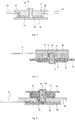
- Figs. 1 and 2 schematically show a magnetic connector 1 according to a first embodiment of the present invention.
- a body of the magnetic connector has a circular cross section and includes a first positive electrode conductor 4, a first insulator 5, a first magnet 6, a first negative electrode conductor 7, a first latch 3, an outer insulating cover 9, a PCB 20 and a first peripheral insulator 21.
- the outer insulating cover 9 forms the body of the magnetic connector.
- the body has a mounting cavity (not shown).
- the PCB 20 is received in the bottom of the mounting cavity.
- An opening of the mounting cavity faces the first peripheral insulator 21.
- the first positive electrode conductor 4 is a first conductive terminal disposed on a side of the PCB 20 in a direction towards the opening of the mounting cavity and located at the center of the PCB 20.
- the first magnet 6 is arranged along the circumference of the PCB 20 and on the same side as the first conductive terminal.
- the magnet has a hollow cylindrical shape, in which the hollow portion is configured to be in muff-coupling with the first conductive terminal. That is, the first conductive terminal extends outwards through the hollow portion of the magnet.
- the first insulator 5 is a first anti-off device dedicated to the first positive electrode conductor 4 and comprises a hollow cylinder and a circular portion bordering the hollow cylinder.
- the hollow cylinder surrounds the first positive electrode conductor 4, and the circular portion, the center of which is hollow for passing the first positive electrode conductor 4, is used to prevent the first magnet from touching the PCB 20.
- the insulator can be imagined having a "hat" shape which is hollow at the top.
- the first negative electrode conductor 7 serves to surround the first magnet 6.
- the first latch 3 may be set between the positive electrode conductor 4 and the PCB and soldered onto the PCB for fixing the first positive electrode conductor 4, the first insulator 5, the first magnet 6, and the first negative electrode conductor 7, etc. on the PCB 20.
- the outer insulating cover 9 and the first peripheral insulator 21 enclose all the above components in the mounting cavity of the body to prevent the occurrence of electric leakage phenomenon.
- the circular magnetic connector may also include the first positive electrode conductor 4, the first insulator 5, the first magnet 6, the first negative electrode conductor 7, the PCB 20, an inner insulating cover 90, and the outer insulating cover 9.
- the magnetic connector in this embodiment does not include a latch.
- the components of the connector are shaped such that the first positive electrode conductor is received in a hollow portion of the first insulator, the first insulator is accommodated in a hollow portion of the first magnet, and the first positive electrode conductor, the first insulator and the first magnet are enclosed within the first negative electrode conductor, all of which are soldered (or by other fixing means) on the PCB 20.
- a wiring harness 8 may be drawn outwards from the cylindrical side of the outer insulating cover 9, one end of which is connected to the PCB 20 in the body, and the other end of which may be equipped with various interfaces for electrical connection with other external devices.
- the wiring harness 8 may be led outwards from the top circular surface of the outer insulating cover 9, as shown in Fig. 17 .
- the wiring harness 8 and the magnetic connector 1 may thus form a magnetic connection 40.
- the first insulator 5 is concave at an end of the first positive electrode conductor 4, forming a circular recess (i.e., a limiting hole) that can receive a portion of a second insulator of an external magnetic connector which embraces an external second conductive terminal (equivalent to at least a portion of the second conductive terminal) when the second conductive terminal contacts (in the manner of abutting-joint or plugging-contact or the like) the first conductive terminal (i.e., the first positive electrode conductor 4) of the magnetic connector in this embodiment along an extending direction of the first positive electrode conductor 4 (hereinafter referred to as an axial direction).
- a circular recess i.e., a limiting hole
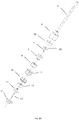
- the above magnetic connector can serve as a male base, while a magnetic connector 2 according to a second embodiment of the present invention shown in Figs. 3 and 4 can serve as a female base which can be used with the magnetic connector 1 in Figs. 1 and 2 cooperatively.
- the magnetic connector which is also circular includes a second peripheral insulator 10, a second negative electrode conductor 11, a second positive electrode conductor 12, a second magnet 13, a second insulator 14, a second latch 15 and a PCB 16.
- the body and the mounting cavity are not shown.
- the PCB 16 is received in the bottom of the mounting cavity. An opening of the mounting cavity is towards the second peripheral insulator 10.
- the second positive electrode conductor 12 is a second conductive terminal disposed on a side of the PCB 16 towards the second peripheral insulator 10 and located at the center of the circular PCB.
- the second magnet 13 has a hollow cylindrical shape and is arranged on the same side of the PCB 16 as the first conductive terminal. The hollow portion of the second magnet 13 embraces the second positive electrode conductor. In other words, the second positive electrode conductor extends through the hollow portion of the second magnet.
- the second insulator 14 is a second detachment prevention device dedicated to the second positive electrode conductor 12.
- the insulator is in the shape of a top-hollow "hat” comprising a hollow cylinder and a circular portion adjoining to the hollow cylinder.
- the hollow cylinder encloses the second positive electrode conductor 12.
- the circular portion prevents the second magnet 13 from contacting the PCB 16.
- the center of the circular portion is hollow for passing the second positive electrode conductor.
- the second negative electrode conductor 11 surrounds the second conductive terminal 12, the second magnet 13 and the second insulator 14.
- the second latch 15 and the second negative electrode conductive body 11 are electrically connected by a snap fit and soldered together with the PCB 16 to form a negative electrode of a circuit.
- the second peripheral insulator 10, the second negative electrode conductor 11, the second magnet 13 and the second insulator 14 may be integrally injection-molded.
- the second positive electrode conductor 12, the second latch 15 and the PCB 16 may be soldered together.
- the injection-molded portion and the soldered portion are locked together.
- the second outer insulating cover 18 (shown in Figs. 5-7 ) and the peripheral insulator 10 enclose all of the above components in the mounting cavity of the body to prevent electric leakage.
- the circular magnetic connector 2 may also include the second negative electrode conductor 11, the second positive electrode conductor 12, the second magnet 13, the second insulator 14, and the PCB 16.
- the second negative electrode conductor is divided into two parts, the bottom of which is in the form of a copper ring. It is easy to manufacture the negative electrode conductor of the female base since it has been divided into two separate parts. Alternatively, these two parts can be assembled by riveting when they are placed respectively on the front and back surfaces of a garment.
- the second insulator 14 protrudes at an end of the second positive electrode conductor 12. That is, a portion of the second insulator 14, which surrounds the second conductive terminal, protrudes with respect to a plane where the second magnet 13 locates.
- the portion of the second insulator enclosing the end of the second conductive terminal 12 that forms the protrusion may be inserted into a recess, for example the limiting hole, of another magnetic connector (male base), when the second conductive terminal is in contact with a first conductive terminal of the male base in an axial direction of the first conductive terminal in the manner of abutting-joint or plugging-contact etc.). In this way it can prevents the connection formed by attraction between the male base and the female base through the magnets from moving in a direction transverse to the axial direction or along a surface of the peripheral insulator.
- the positive electrode conductor of the magnetic connector is soldered onto the PCB to form a positive electrode of a circuit and the negative electrode conductor is soldered or riveted on the PCB to form a negative electrode of the circuit.
- the male base is in contact with the female base, one positive electrode conductor must contact the other positive electrode conductor and one negative electrode conductor must contact the other negative electrode conductor, otherwise short-circuit may occur in the circuit.
- the first conductive terminal may be a POGO PIN
- the second conductive terminal may be in the form of a socket that can be plugged.
- the male base 1 and the female base 2 are connected together to form conduction by a mutual attraction between the magnets. Both of the conductive terminals of the male base 1 and the female base 2 are abutted conducting through the attraction of the magnets and thus conductive.
- the recess of the male base and the protrusion of the female base may match and engage with each other. Therefore, the anti-off devices of the male base and the female base make the connection therebetween stable, so that the connection between the conductive terminals of the two bases is stable.
- the female base 2 or the male base 1 can be fixed on a carrier 19 ( Figs. 4-8 ) by perforating them as a button.
- the carrier 19 can be a housing of a wearable device or a wearable garment. The beneficial effects are that the male base or the female base is installed on a garment or a wearable housing so as to be charged in time as required, and can be used as a decoration such as a button when not in use, which is convenient for carrying and quick application.
- the beneficial effect of the above structure is that magnets are arranged in the structures of the magnetic connector 2 (female base) and the magnetic connector 1 (male base), which not only serve to attract each other so as to enable the male base and the female base to be firmly connected, but can also realize circuit or data conduction and charging functions.
- FIGs. 5-7 schematically show a magnetic connector as a female base in accordance with another embodiment of the present invention.
- the second peripheral insulator 10, the second negative electrode conductor 11, the second magnet 13 and the second insulator 14 of the magnetic connector 2 are injection-molded as a first component.
- the second positive electrode conductor 12, the second latch 15 and the second PCB 16 are soldered to a second component.
- the first component and the second component may be locked and connected together by ultrasonic welding or riveting.
- the female base 2 may be provided on the carrier 19.
- the carrier 19 may be a cloth or plastic housing.
- the carrier 19 may be set between the first component and the second component of the magnetic connector 2.
- the first component and the second component can form a negative electrode of a circuit through a snap fit between them.
- the first peripheral insulator 21, the first insulator 5, the first negative electrode conductor 7 and the first magnet 6 of the male base 1 are connected as a third component.
- the first PCB 20, the wiring harness 8, the first positive electrode conductor 4 and the first outer insulating cover 9 are connected as a fourth component.
- the carrier 19 may be positioned between the third component and the fourth component of the male base 1.
- the carrier 19 may be provided between the second peripheral insulator 10 and the second outer insulating cover 18 of the female base 2.
- the carrier 19 may be provided between the second peripheral insulator 10 and the second latch 15.
- the material of the latch may be brass.
- the material of the magnet may be aluminum-ferrum-boron. The components can ensure the strength while the thickness keeps small, so that the male base and the female base are more structurally fit to reduce space volume.
- the structure of the (female) magnetic connector 2 can have several different installation methods. In different installation methods, there are slight changes in the volume and structure of the product itself, and the openings in the garment are different in size.
- the second negative electrode conductor 11 is placed into a mold for injection-molding to form the second peripheral insulator 10.
- the second magnet 13 is placed in a cavity of the second negative electrode conductor 11.
- the combination of the second negative electrode conductor 11, the second peripheral insulator 10 and the second magnet 13 is placed into the mold for injection molding to form the second insulator 14.
- the second PCB 16 and the second latch 15 are placed with a fixture and subject to reflow welding.
- the second positive electrode conductor 12 is soldered to a combination of the second PCB 16 and the second latch 15.
- the second negative electrode conductor 11, the second peripheral insulator 10 and the second magnet 13 as a first component and the second positive electrode conductor 12, the second PCB 16 and the second latch 15 as a second component are riveted together.
- the garment is placed into the second component. Then the first component and the second component are riveted together to achieve conduction of positive and negative electrodes and charging or data transmission.
- the second peripheral insulator 10 is formed through injection-molding by placing the second negative electrode conductor 11 into a mold. Then the molded second negative electrode conductor 11 and the second peripheral insulator 10 are placed into the mold to perform injection molding for the second time to form the second insulator 14.
- the above parts belong to a first component.
- the second latch 15 is pasted on the second PCB 16 and subject to reflow welding. Then the second positive electrode conductor 12 is soldered to the second PCB 16 and the second magnet 13 is installed on the second PCB 16, both of which are fixed by the second latch 15 to form a subassembly which is then placed into the mold to obtain the second outer insulating cover 18 through injection-mold.
- the garment In use, the garment is placed between the parts of the second component. Then the first component and the second component are riveted together to achieve conduction of the positive and negative electrodes and charging.
- the magnetic connector in this mode is different in that the abutting surface for conduction is thinned, and the diameter of the opening for installing the cloth is changed from 8 mm to 4 mm.
- the second peripheral insulator 10 is formed through injection-molding,by placing the second negative electrode conductor 11 into a mold .
- the molded second negative electrode conductor 11 and the second peripheral insulator 10 are placed into the mold to perform injection molding for the second time and form the second insulator 14.
- the second magnet 13 is placed in a cavity of the second negative electrode conductor 11, both of which are then placed into the mold and rubber coated to form another layer of second peripheral insulator 10, thereby forming a first component.
- the second latch 15 is pasted on the second PCB 16 and subject to reflow welding.
- the second positive electrode conductor 12 is soldered to the second PCB 16, and then placed into the mold for injection molding the second outer insulating cover 18, thus forming a second component.
- the garment With the first component and the second component assembled in the above mode, the garment is placed between the parts of the second component in use. The first component and the second component are then riveted together to form a unit for charging or data transmission.
- the second outer insulating cover 18 is thinned while the opening of the cloth is smaller.
- the installed second wiring harness 17 is located outside the garment, and an internal electrical conductor of the garment is fastened onto the external second negative electrode conductor 11, while an external negative ring conductor is soldered to the second PCB 16.
- the second peripheral insulator 10 is formed through injection-molding by placing the second negative electrode conductor 11 into a mold.
- the second magnet 13 is placed in a cavity of the second negative electrode conductor 11 and then placed into the mold to perform injection molding for second time so as to form the second insulator 14, thus obtaining a first component.
- the second latch 15 is installed on the second PCB 16 and subject to reflow welding.
- the second positive electrode conductor 12 is soldered to the second PCB 16.
- the second positive electrode conductor 12, the second PCB 16 and the second latch 15 form a second component.
- the first component and the second component are riveted together. All the riveted components are placed in the mold for rubber coating to mold the second peripheral insulator 10.
- the second outer insulating cover 18 is an injection-molded plastic part and performs ultrasound with the second peripheral insulator 10 to clamp the garment, i.e., the carrier 19.
- the outlet method and the opening size of the garment in this mode are changed, which is beautiful in appearance and more practical.
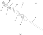
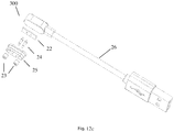
- Figs. 9 and 10 show a third embodiment and a fourth embodiment of the magnetic connector in accordance with the present invention.
- a magnetic connector 100 male base
- the magnetic connector includes a PCB 22, a first magnet 23, a first conductive terminal 24, a first insulating bracket 25, an inner insulating cover 27, and an outer insulating cover 28.
- the inner insulating cover 27 forms a body of the magnetic connector in this embodiment.
- the body has a mounting cavity (not shown).
- the PCB 22 is received at the bottom of the mounting cavity.
- the PCB 22 has a rectangular structure (which may have rounded or not rounded corners) with a length direction and a width direction. Particularly, the length of the PCB 22 in the length direction is greater than that in the width direction.
- the first conductive terminal 24 including a number of posts are centrally positioned on a side of the PCB 22 towards the top of the mounting cavity and are arranged in rows along the length direction of the PCB with constant spaces.
- the first conductive terminal 24 extends towards the top of the mounting cavity.
- the first conductive terminal comprised six posts.
- the first magnet 23 is located on the same side as the first conductive terminal 24 and includes two segments arranged on both sides of the first conductive terminal 24 in the width direction.
- the first magnet has a contact surfaces for mutual attraction with a contact surfaces of an external second magnet.
- the shape of the two segments of magnet can be cylindrical, square or other shapes as long as the contact surfaces are flat.
- the first insulating bracket (i.e., insulating bushing) 25 is a first anti-off dedicated to the first conductive terminal 24, and includes eight limiting holes ( Fig. 9 ), of which the middle six holes are used to enclose the first conductive terminal 24, and the other two are used for embracing the first magnet 23.
- the outer insulating cover 28 may coat the inner insulating cover 27, to prevent leakage of electricity.
- a wiring harness 26 is drawn outwards from the surface of the outer insulating cover 28.
- One end of the wiring harness 26 is connected to the PCB 22 in the body, and the other end can be installed with various interfaces for electrical connection with other external devices.
- the wiring harness 26 connecting the PCBs may be led out through holes in the inner insulating cover 27 and the outer insulating cover 28 in the length direction or the width direction or a direction opposite to the extending direction of the conductive terminal, as shown in Fig. 16 .
- the wiring harness 26 and the magnetic connector 100 may thus constitute a magnetic connection 400.
- the first insulating bracket 25 is recessed inward relative to the extending direction of the first conductive terminal to form a recess.
- the recess may receive an external second conductive terminal or a portion of a device which embraces the end of the second conductive terminal (equivalent to at least a portion of the second conductive terminal) when the second conductive terminal is in contact with the first conductive terminal 24 of the magnetic connector according to this embodiment in the extending direction thereof (hereinafter referred to as an axial direction).
- This makes it possible to prevent a second conductive terminal or a second magnet of another magnetic connector that is in contact with the magnetic connector in this embodiment by attraction between the magnets from moving in a direction transverse to the axial direction.
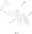
- Fig. 10 shows a magnetic connector 200 as a female base according to a fourth embodiment of the present invention.
- the magnetic connector 200 matches the magnetic connector 100 in the third embodiment.
- the magnetic connector is also in a square shape.
- This magnetic connector includes at least a PCB 29, a second magnet 30, a second conductive terminal 31 and a second insulating bracket 32.
- the magnetic connector includes a body having a mounting cavity (not shown).
- the PCB 29 is received in the bottom of the mounting cavity.
- the PCB 29 has a rectangular structure with a length direction and a width direction (which may also have rounded corners or not rounded corners).
- the length of the PCB 29 in the length direction is greater than the length in the width direction.
- the second conductive terminals 31 are centrally located on one side of the PCB 29 and arranged in rows along the length direction.
- the way in which the second conductive terminal is in contact with an external first conductive terminal is plugging. That is, a part of the conductive terminal, which contacts the external first conductive terminal, is in the form of a pluggable socket.
- the conductive terminal comprises six posts.
- the second magnet 30 is located on the same side as the second conductive terminal and includes two segments arranged on both sides of the conductive terminal in the width direction.
- the two segments of the second magnet have the contact surfaces for mutual attraction with contact surfaces of an external first magnet.
- the shape of the two segments of the second magnet can be cylindrical, square or other shapes as long as the contact surfaces are flat.
- the second insulating bracket (bushing) 32 is a second detachment prevention device dedicated to the second conductive terminal 31 and the second magnet 30.
- the insulating bracket includes eight limiting holes, in which the middle six are used to surround the second conductive terminal 31, and the other two on the outer side are used to surround the second magnet 30.
- the second conductive terminal 31 and the second magnet 30 can protrude from the limiting hole of the second insulating bracket, so that when the external first conductive terminal contacts the second conductive terminal 31 of the magnetic connector 200 along the extending direction (hereinafter referred to as an axial direction) in this embodiment, it can be inserted into the recess of the insulation bushing of the first detachment prevention device.
- the second conductive terminal and/or the second magnet may be inserted into the limiting holes in the insulating bushing (bracket) of the first anti-off device 25. This prevents the second conductive terminal or the second magnet from moving in a direction transverse to the axial direction when the magnetic connector 200 is in contact with another magnetic connector.
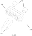
- Figs. 11-14 schematically show other embodiments of the magnetic connector in accordance with the present invention.
- the magnetic connector in this embodiment is different from the third embodiment in that: the conductive terminal comprises three posts; and the insulation bushing of the first anti-off device includes an insulating bracket 101, an inner insulating cover 102 and an outer insulating cover 103.
- the conductive terminals of a magnetic connector 300 (male base) and of a magnetic connector 310 (male base) in this embodiment each include two posts.
- the female base includes two kinds of structures.
- a portion 312 of an insulating bushing 311 embracing the second conductive terminal preferably protrudes with respect to a plane where a second magnet 313 locates, as shown in Fig. 12a , in which the protrusion portion is inserted into a recess (not shown) of an insulating bushing of the male base to form a fixation.
- an insulating bushing of the female base does not protrude with respect to the plane where the second magnet 313 locates.
- a first magnet in this embodiment is in the shape of hollow cylinder (i.e., in the shape of "racetrack") circling the first conductive terminal.
- the racetrack-shaped magnet can be soldered to a PCB by solder paste, which can effectively prevent the magnet from falling off.
- the magnet can also be fixed on a bracket by metal sleeve.
- a magnet of step type i.e., a "U" shaped magnet may be used.
- the insulating bracket (bushing) is accommodated in a hollow portion of the magnet.
- the insulating bracket includes a plurality of limiting holes. The number of the limiting holes is the same as the number of the post in the first conductive terminal.
- the insulating bracket installed on the PCB is aligned with the magnet.
- the first conductive terminal protrudes through the respective limiting holes.
- a magnetic connector (not shown) corresponding to this male base may include second conductive terminal (similar to those in Fig.
- the male and female bases are fixed by inserting the first conductive terminal into the second conductive terminal and may also include an insulating bracket with a plurality of limiting holes so that the first conductive terminal is inserted into the limiting hole of the female base to contact with the second conductive terminal located in the limiting hole, thus keeping a stable connection between the male and female connectors.
- Fig. 14 schematically shows a magnetic connector with five posts of conductive terminal. Similar to the magnet in Fig. 13 , a magnet in Fig. 14 is also hollow cylindrical. The height of an insulating bracket installed on a PCB is higher than that of the magnet. In other words, the insulating bracket protrudes with respect to the plane where the magnet locates. Therefore, a magnetic connector matching the magnetic connector in Fig. 14 is configured such that the height of the insulating bracket is less than the height of the magnet so that the insulating bracket of the magnetic connector in Fig. 14 can be inserted into the hollow portion of the magnet.
- the present invention also provides a magnetic connection member.
- the magnetic connection member includes a magnetic connector as male base and a wiring harness in any one of the above embodiments.
- One end of the wiring harness is connected to a PCB of the magnetic connector, and the other end has, for example, a USB interface connected to an external device.
- the present invention further provides a magnetic connection assembly.
- the magnetic connection assembly includes a first magnetic connector and a second magnetic connector matching with each other and a wiring harness connected to the first magnetic connector.
- the first magnetic connector may be the male base in the embodiment of the present invention
- the second magnetic connector may be the female base in the embodiment of the present invention.
- One end of the wiring harness is connected to a PCB in the first magnetic connector, and the other end can be equipped with various interfaces such as various USB ports for electrical connection with other external devices.
- a magnetic connection assembly is shown with the magnetic connector being circular.
- a portion of the insulating bushing of the female base which surrounds the second conductive terminal 12, protrudes with respect to a plane where the second magnet 13 is.
- the insulating bushing of the male base is configured to receive the portion of the insulating bushing of the female base which surrounds the second conductive terminal 12 when the first conductive terminal 4 is in contact with the second conductive terminal 12 of the female base oppositely in an axial direction and forms conduction to limit displacement of the second conductive terminal in a direction transverse to the axial direction.
- a magnetic connection assembly when the magnetic connector is square.
- the second conductive terminal 31 of the female base protrudes from the second limiting hole.
- the insulating bushing of the male base is configured to receive at least a portion of the second conductive terminal 12 of the female base (the portion protruding from the second limiting hole) when the first conductive terminal 24 is in contact with the second conductive terminal 12 oppositely in an axial direction and forms conduction to limit displacement of the second conductive terminal 12 in a direction transverse to the axial direction.
- the second magnet 13 of the female base protrudes from the second limiting hole.
- the insulating bushing of the male base is accordingly configured to receive at least a portion of the second magnet 13 (i.e., the portion protruding from the second limiting hole) when the first magnet 25 is magnetically attracted to the second magnet 13 of the female base oppositely in an axial direction to limit displacement of the second magnet 13 in a direction transverse to the axial direction.
- the conductive terminal (whether the first conductive terminal or the second conductive terminal) includes a positive pole posts and a negative pole posts.
- the negative pole post(s) may be arranged in the center of the PCB and the positive pole post(s) may be symmetrically arranged with respect to the negative pole post(s).
- the two segments of the magnet arranged on both sides of the conductive terminal have the same magnetic poles. For example, referring to Fig. 13 , the middlemost post among the seven posts is negative, and the remaining three left posts and three right posts are positive all. Each two segments of the magnet on both sides of the conductive terminal are the same type of N poles or S poles.
- the middle of the three posts is negative, and the posts at both sides are positive.
- the magnetic connector can be connected to another matched magnetic connector without distinguishing the connecting direction of the conductive terminals, so that a USB function capable of charging and transmitting data on the front and back surfaces can be realized.
- the conductive terminals may further include the post(s) for data transmission.
- the magnetic connector can also be used unidirectionally.
- the post in the middle may be a data port, and the remaining posts on both sides are negative and positive respectively. This arrangement with more data transmission interfaces (i.e., data ports) can achieve more functions to data transfer.
- the two segments of magnet arranged on both sides of the conductive terminal may have different poles, especially when the conductive terminal is provided with data ports as described above.
- two magnetic connectors male base and female base
- the magnets of two magnetic connectors can automatically identify the attraction direction and form a connection, playing a foolproof role.
- a short-circuit protection circuit can also be arranged between the positive electrode conductor and the negative electrode conductor of the conductive terminal, as shown in Fig. 15 , to realize overcurrent and short circuit protection functions.
- the circuit consists of three parts, including a main chip U1 controlling switch output and a sampling of the output state, a switch MOS tube Q1 being connected to the output, and a switch Q2 being connected to the output to check the output status.
- Resistors R2, R5 and capacitor C5 form a sampling loop of the output current. When output load over-current occurs, an output current flows across R2 to form a voltage drop. The voltage drop is provided to pin 7 of U1 after being limited by R5 and filtered by C5.
- U1 adjusts output with PWM control through pin 7, and adjusts the on-time of Q1 to control the magnitude of the output current to achieve output over-current protection.
- voltage VOUT+ changes.
- the voltage is lower than a certain value in a short time, the voltage flows through R4 to Q2 and will be rapidly shown in pin 5 of U1.
- U1 turns off Q1 by controlling pin 6 after performing data determination, to achieve short circuit protection.
- Figs. 18 and 19 show two embodiments of a garment or protective clothing for intelligent heating in accordance with the present invention.
- a heating unit is fixed between a first carrier 181 and a second carrier 182 without exposing from the second carrier.
- a heating component 183 and a magnetic connector are connected together by a wiring harness.
- the first carrier or the second carrier is provided with a via hole 184 at an arbitrary position.
- the diameter of via hole is larger than an outer diameter A of a body 180 of the magnetic connector.
- the outer diameter A passes through, for example, the via hole 184 disposed on the first carrier.
- the body 180 of the magnetic connector is fixed on the first carrier (being clamped between the rear cover 185 and the body of the magnetic connector and being not easy to fall off) by riveting pressure.
- the rear cover and the body of the magnetic connector are fixed on the first carrier by interference riveting.
- the polarity of the magnetic connector on the carrier is N pole
- the polarity on a power supply device 186 (equipped with a magnet battery box and a magnet wire) is S.
- the battery box has a power switch and a current control device. The user can adjust the temperature through a temperature control device or perform other control operations.
- the PCB on the rear cover of the magnetic connector can have temperature detection and temperature protection functions.
- the PCB on the rear cover of the magnetic connector can further have a Bluetooth control circuit.
- the heating product can be controlled and adjusted by a cable with a temperature control switch function.
- the heating product can perform temperature control with a mobile power supply having a temperature control function.
- the conductive terminal of the magnetic connector includes at least two PINs. In the heating product, the switch is assembled on the first carrier.
- a first magnet interface 191 and a second magnet interface 192 are fixed to a first fabric sheet 193 by riveting.
- a heating sheet 195 is soldered to the second magnet interface.
- the first fabric sheet 193 and a second fabric sheet 194 fix and bond the heating sheet.
- the other side of the first fabric sheet is affixed with a silicone sheet 196, which can be affixed to human skin.
- a tablet 197 is placed in the middle gap of the silicone sheet.
- the controller 170 includes an upper case 171, a switch button 172, an indicator light 173, a PCBA 174, an encapsulating inner mold 175, an encapsulating outer mold 176, and a hardware steel piece 177.
- a magnetic input interface 178 including the first magnet interface 191 and the second magnet interface 192
- the controller controls the heating sheet to generate heat and heat the medicine tablet and maintain the temperature so as to maximize the efficacy of the tablet.
- the preparation method is as follows:
Landscapes
- Engineering & Computer Science (AREA)
- Microelectronics & Electronic Packaging (AREA)
- Textile Engineering (AREA)
- Environmental & Geological Engineering (AREA)
- Health & Medical Sciences (AREA)
- General Health & Medical Sciences (AREA)
- Physical Education & Sports Medicine (AREA)
- Details Of Connecting Devices For Male And Female Coupling (AREA)
- Professional, Industrial, Or Sporting Protective Garments (AREA)
- Outerwear In General, And Traditional Japanese Garments (AREA)
Applications Claiming Priority (2)
| Application Number | Priority Date | Filing Date | Title |
|---|---|---|---|
| CN201611206241.7A CN106505363B (zh) | 2016-12-23 | 2016-12-23 | 磁性电极纽扣 |
| PCT/CN2017/118041 WO2018113780A1 (fr) | 2016-12-23 | 2017-12-22 | Bouton d'électrode magnétique |
Publications (3)
| Publication Number | Publication Date |
|---|---|
| EP3364506A1 true EP3364506A1 (fr) | 2018-08-22 |
| EP3364506A4 EP3364506A4 (fr) | 2018-12-26 |
| EP3364506B1 EP3364506B1 (fr) | 2021-09-29 |
Family
ID=58333804
Family Applications (1)
| Application Number | Title | Priority Date | Filing Date |
|---|---|---|---|
| EP17859338.0A Active EP3364506B1 (fr) | 2016-12-23 | 2017-12-22 | Bouton d'électrode magnétique |
Country Status (6)
| Country | Link |
|---|---|
| US (1) | US10297950B2 (fr) |
| EP (1) | EP3364506B1 (fr) |
| JP (1) | JP6835963B2 (fr) |
| KR (1) | KR102041350B1 (fr) |
| CN (2) | CN106505363B (fr) |
| WO (1) | WO2018113780A1 (fr) |
Cited By (3)
| Publication number | Priority date | Publication date | Assignee | Title |
|---|---|---|---|---|
| EP3467956A1 (fr) * | 2017-08-23 | 2019-04-10 | Amphenol Phitek Limited | Vérin magnétique circulaire |
| WO2021204813A1 (fr) * | 2020-04-07 | 2021-10-14 | Arfaoui Faisel | Système de connexion pour établir une connexion électriquement conductrice amovible et connecteurs |
| EP4324742A3 (fr) * | 2017-08-23 | 2024-04-17 | Amphenol Phitek Limited | Connecteur électrique |
Families Citing this family (54)
| Publication number | Priority date | Publication date | Assignee | Title |
|---|---|---|---|---|
| US20160003270A1 (en) * | 2013-03-15 | 2016-01-07 | L. Christopher Franklin | Mounting apparatus |
| CN106505363B (zh) * | 2016-12-23 | 2019-11-26 | 深圳市泰科汉泽精密电子有限公司 | 磁性电极纽扣 |
| CN107146965A (zh) * | 2017-07-05 | 2017-09-08 | 商洛市虎之翼科技有限公司 | 一种磁吸式充放电接头 |
| CN107221775A (zh) * | 2017-07-05 | 2017-09-29 | 商洛市虎之翼科技有限公司 | 一种磁吸式连接结构 |
| CN207078277U (zh) * | 2017-08-21 | 2018-03-09 | 东莞镁迪电子有限公司 | 一种电动车的电源连接结构 |
| CN107631188A (zh) * | 2017-10-30 | 2018-01-26 | 商洛市虎之翼科技有限公司 | 一种磁吸式多开关照明装置 |
| DE102017125846A1 (de) * | 2017-11-06 | 2019-05-09 | Fidlock Gmbh | Verbindungsvorrichtung zum lösbaren Verbinden zweier Baugruppen |
| EP3729480A4 (fr) * | 2017-12-21 | 2022-01-05 | Ideal Industries Inc. | Système de verrouillage de force convertible |
| US10717019B2 (en) * | 2018-03-09 | 2020-07-21 | Toyish Labs Inc. | Flexible construction unit, kit, and method for constructing a structure |
| WO2019193564A1 (fr) * | 2018-04-06 | 2019-10-10 | Fischer Connectors Holding S.A. | Connecteur multipolaire |
| US11616324B2 (en) | 2018-04-06 | 2023-03-28 | Conextivity Group Sa | Multipolar connector |
| JP7093259B2 (ja) * | 2018-07-18 | 2022-06-29 | 日本航空電子工業株式会社 | 衣服用コネクタ |
| US10522943B1 (en) * | 2018-09-21 | 2019-12-31 | Calista A. Termini | Magnetically securing detachable electronic cable assembly and method |
| EP3637963B1 (fr) * | 2018-10-12 | 2024-02-07 | AT&S Austria Technologie & Systemtechnik Aktiengesellschaft | Structures porteuses de composants reliées par des structures d'aimant coopérants |
| CN111224254B (zh) | 2018-11-27 | 2022-04-05 | 上海莫仕连接器有限公司 | 第一连接器、第二连接器及电连接器组件 |
| CN109529189B (zh) * | 2018-12-21 | 2022-04-26 | 厦门固立电子科技有限公司 | 一种基于智能医疗设备的磁控三电极加载与分离装置及方法 |
| CN109892718B (zh) * | 2019-03-15 | 2024-03-22 | 安徽商贸职业技术学院 | 一种基于太阳能的可加热衣服 |
| KR20220003170A (ko) * | 2019-05-30 | 2022-01-07 | 에코너스 인코퍼레이티드 | 보조 심전도(ecg) 조립체 및 보조 ecg 조립체를 포함하는 임상 데이터 획득 시스템(auxiliary electrocardiogram (ecg) assemblies and clinical data acquisition systems including auxiliary ecg assemblies) |
| CN112271495B (zh) * | 2019-07-08 | 2022-07-05 | 上海莫仕连接器有限公司 | 第一连接器、第二连接器及电连接器组合 |
| KR102243156B1 (ko) * | 2019-07-08 | 2021-04-21 | 서울과학기술대학교 산학협력단 | 단추형 동축 커넥터 |
| JP7232144B2 (ja) * | 2019-07-19 | 2023-03-02 | 日本航空電子工業株式会社 | コネクタ |
| JP7232143B2 (ja) * | 2019-07-19 | 2023-03-02 | 日本航空電子工業株式会社 | コネクタ |
| KR102304175B1 (ko) * | 2019-08-01 | 2021-09-24 | 주식회사 헤카텍 | 신축성 전선, 이를 이용한 ems 수트 및 시스템 |
| CN110459929A (zh) * | 2019-09-11 | 2019-11-15 | 龙其烈 | 一种磁吸充电线 |
| CN112510403B (zh) | 2019-09-16 | 2023-02-03 | 上海莫仕连接器有限公司 | 第一连接器、第二连接器及电连接器组件 |
| CN112636071B (zh) * | 2019-09-24 | 2023-02-07 | 华为技术有限公司 | 一种连接器、电子设备 |
| US11258189B2 (en) * | 2019-10-03 | 2022-02-22 | Japan Aviation Electronics Industry, Limited | Connector and connecting method |
| JP7348024B2 (ja) * | 2019-10-24 | 2023-09-20 | 日本航空電子工業株式会社 | コネクタおよび接続方法 |
| US11760198B2 (en) * | 2019-11-15 | 2023-09-19 | Ryan D. Aberle | Magnetic tether switch |
| KR200493236Y1 (ko) * | 2019-12-30 | 2021-02-24 | 주식회사 한국가스기술공사 | 전위측정용 케이블 연결구조체 |
| FR3107399B1 (fr) * | 2020-02-13 | 2022-06-03 | Schneider Electric Ind Sas | Connecteur magnétique et groupe de connecteurs magnétiques |
| US11289849B2 (en) * | 2020-07-08 | 2022-03-29 | Jayesh Jani | Magnetized data connector assembly |
| CN114503372B (zh) * | 2020-08-24 | 2024-03-19 | 深圳市华思旭科技有限公司 | 一种导电端子、连接器、充电器以及应急启动电源 |
| US11462855B2 (en) * | 2020-08-28 | 2022-10-04 | Te Connectivity Solutions Gmbh | Magnetic-enabled quick disconnect electrical connector |
| CN112072362A (zh) * | 2020-09-11 | 2020-12-11 | 苏州凯毅斯智能驱动技术有限公司 | 一种带通讯耐大电流拨插的连接器 |
| CN112103745A (zh) * | 2020-09-21 | 2020-12-18 | 深圳碳美医疗有限公司 | 一种智能直流数码显示控温连接线及制作方法 |
| US11103699B1 (en) * | 2020-11-11 | 2021-08-31 | Zida Llc | Nerve stimulation garment |
| CN114762641A (zh) * | 2021-01-12 | 2022-07-19 | 鹏鼎控股(深圳)股份有限公司 | 智能调温织物 |
| CN115149329A (zh) * | 2021-03-30 | 2022-10-04 | 正凌精密工业(广东)有限公司 | 连接装置及其与对接装置的组合 |
| CN113178733B (zh) * | 2021-04-22 | 2022-04-15 | 东莞市思索连接器有限公司 | 一种两件式经济型连接器 |
| CN113422229B (zh) * | 2021-05-25 | 2022-06-24 | 深圳市康澄科技有限公司 | 一种连接器 |
| USD1023980S1 (en) * | 2022-04-11 | 2024-04-23 | Brooke Erin Desantis | Control for heated wearables |
| USD1023983S1 (en) * | 2022-04-11 | 2024-04-23 | Brooke Erin Desantis | Control for heated wearables |
| USD1022926S1 (en) * | 2022-06-08 | 2024-04-16 | Brook Erin DeSantis | Control for heated wearables |
| USD1021820S1 (en) * | 2022-06-08 | 2024-04-09 | Brooke Erin Desantis | Control for heated wearables |
| USD1022925S1 (en) * | 2022-06-08 | 2024-04-16 | Brook Erin DeSantis | Control for heated wearables |
| USD1006767S1 (en) * | 2022-06-08 | 2023-12-05 | Brooke Erin Desantis | Control for heated wearables |
| USD1021827S1 (en) * | 2022-06-08 | 2024-04-09 | Brooke Erin Desantis | Control for heated wearables |
| USD1022437S1 (en) * | 2022-06-08 | 2024-04-16 | Brook Erin DeSantis | Control for heated wearables |
| USD1016024S1 (en) * | 2022-06-08 | 2024-02-27 | Brooke Erin Desantis | Control for heated wearables |
| USD1021819S1 (en) * | 2022-06-08 | 2024-04-09 | Brook Erin DeSantis | Control for heated wearables |
| USD1008197S1 (en) * | 2022-06-08 | 2023-12-19 | Brooke Erin Desantis | Control for heated wearables |
| USD1021818S1 (en) * | 2022-06-08 | 2024-04-09 | Brook Erin DeSantis | Control for heated wearables |
| USD1007445S1 (en) * | 2023-08-30 | 2023-12-12 | Chenhui Li | Heated apparel controller |
Family Cites Families (35)
| Publication number | Priority date | Publication date | Assignee | Title |
|---|---|---|---|---|
| US4025964A (en) * | 1976-07-30 | 1977-05-31 | The United States Of America As Represented By The Administrator Of The National Aeronautics And Space Administration | Magnetic electrical connectors for biomedical percutaneous implants |
| DE102005007598A1 (de) * | 2005-02-18 | 2006-08-24 | Fraunhofer-Gesellschaft zur Förderung der angewandten Forschung e.V. | Bekleidungsstück |
| US7641476B2 (en) * | 2005-06-30 | 2010-01-05 | David Didur | Rotatable magnetic electrical connector |
| US7462035B2 (en) * | 2005-07-27 | 2008-12-09 | Physical Optics Corporation | Electrical connector configured as a fastening element |
| US7331793B2 (en) * | 2005-12-16 | 2008-02-19 | Motorola, Inc. | Magnetic connector |
| CN201025645Y (zh) * | 2007-02-08 | 2008-02-20 | 葛兆民 | 磁力电信号连接座与连接头 |
| JP6042430B2 (ja) * | 2011-07-18 | 2016-12-14 | エンピ・インコーポレイテッド | 電極、電極システム及びその製造方法 |
| US9065205B2 (en) * | 2011-08-11 | 2015-06-23 | Apple Inc. | Connector insert having a cable crimp portion with protrusions and a receptacle having label in the front |
| JP5784516B2 (ja) * | 2012-02-01 | 2015-09-24 | モリト株式会社 | 通電ホック |
| KR20140067356A (ko) * | 2012-11-26 | 2014-06-05 | 삼성전자주식회사 | 케이블 컨넥터 장치 |
| US9391394B2 (en) * | 2012-12-21 | 2016-07-12 | Koninklijke Philips N.V. | Magnetic connector assembly |
| US9055879B2 (en) * | 2013-06-14 | 2015-06-16 | Suunto Oy | Device and method for assembling an electronic device and a flexible element for facilitating assembly of electronic components |
| US9312632B2 (en) * | 2013-09-27 | 2016-04-12 | Genesis Technology Usa, Inc. | Heat resistant magnetic electrical connector |
| KR20150047780A (ko) * | 2013-10-25 | 2015-05-06 | 삼성전자주식회사 | 전기 커넥터를 구비하는 전자 장치 |
| ES2834486T3 (es) * | 2014-02-12 | 2021-06-17 | Swemac Innovation Ab | Dispositivo de direccionamiento |
| JP6182093B2 (ja) * | 2014-03-10 | 2017-08-16 | ホシデン株式会社 | コネクタ及びこれを備えた電子機器 |
| EP3154624A1 (fr) * | 2014-06-12 | 2017-04-19 | Heartware, Inc. | Connecteur percutané avec capuchon magnétique et procédés d'utilisation associés |
| CN104124583A (zh) * | 2014-06-25 | 2014-10-29 | 深圳市泰比特科技有限公司 | 一种穿戴式产品充电数据传输线连接装置 |
| CN204156545U (zh) | 2014-07-16 | 2015-02-11 | 李红兴 | 一种小功率电器无线充电装置 |
| US9991628B2 (en) * | 2014-07-21 | 2018-06-05 | Daniel J Daoura | Quick connect magnetic interface products and methods |
| US9515420B2 (en) * | 2014-07-21 | 2016-12-06 | Daniel J Daoura | Quick connect interface |
| US20160105047A1 (en) * | 2014-10-10 | 2016-04-14 | Aibc International, Llc | Mobile device mounting and charging system |
| CN204156245U (zh) * | 2014-10-15 | 2015-02-11 | 深圳市德兴顺科技有限公司 | 多功能磁扣 |
| CN204144573U (zh) * | 2014-10-31 | 2015-02-04 | 张汝良 | 磁性易连电器接头 |
| CN105790323A (zh) * | 2014-12-15 | 2016-07-20 | 海洋王照明科技股份有限公司 | 手电筒的充电装置 |
| US9983747B2 (en) * | 2015-03-26 | 2018-05-29 | Google Llc | Two-layer interactive textiles |
| CN106159525B (zh) * | 2015-03-27 | 2018-03-06 | 富士康(昆山)电脑接插件有限公司 | 磁吸式连接器及线缆连接器组件 |
| GB201506418D0 (en) * | 2015-04-15 | 2015-05-27 | Connectors Ltd Ab | Connector assembly |
| CN105281116A (zh) * | 2015-05-29 | 2016-01-27 | 维沃移动通信有限公司 | 一种吸附式连接器及其连接方法 |
| US9848071B2 (en) * | 2015-08-28 | 2017-12-19 | Jean-Michel Andre Thiers | Rotatable electrical connector |
| US9941627B2 (en) * | 2015-09-30 | 2018-04-10 | Apple Inc. | Magnetic surface contacts |
| US9837760B2 (en) * | 2015-11-04 | 2017-12-05 | Google Inc. | Connectors for connecting electronics embedded in garments to external devices |
| JP3204474U (ja) * | 2016-03-16 | 2016-06-02 | 裕雄 范 | 充電ジョイント |
| CN206619752U (zh) * | 2016-12-23 | 2017-11-07 | 深圳市泰科汉泽精密电子有限公司 | 磁性电极钮扣 |
| CN106505363B (zh) * | 2016-12-23 | 2019-11-26 | 深圳市泰科汉泽精密电子有限公司 | 磁性电极纽扣 |
-
2016
- 2016-12-23 CN CN201611206241.7A patent/CN106505363B/zh active Active
-
2017
- 2017-12-22 JP JP2019526000A patent/JP6835963B2/ja active Active
- 2017-12-22 EP EP17859338.0A patent/EP3364506B1/fr active Active
- 2017-12-22 WO PCT/CN2017/118041 patent/WO2018113780A1/fr unknown
- 2017-12-22 KR KR1020197012798A patent/KR102041350B1/ko active IP Right Grant
- 2017-12-22 CN CN201780002792.8A patent/CN109075499B/zh active Active
-
2018
- 2018-03-23 US US15/934,158 patent/US10297950B2/en active Active
Cited By (3)
| Publication number | Priority date | Publication date | Assignee | Title |
|---|---|---|---|---|
| EP3467956A1 (fr) * | 2017-08-23 | 2019-04-10 | Amphenol Phitek Limited | Vérin magnétique circulaire |
| EP4324742A3 (fr) * | 2017-08-23 | 2024-04-17 | Amphenol Phitek Limited | Connecteur électrique |
| WO2021204813A1 (fr) * | 2020-04-07 | 2021-10-14 | Arfaoui Faisel | Système de connexion pour établir une connexion électriquement conductrice amovible et connecteurs |
Also Published As
| Publication number | Publication date |
|---|---|
| US20180212359A1 (en) | 2018-07-26 |
| EP3364506B1 (fr) | 2021-09-29 |
| EP3364506A4 (fr) | 2018-12-26 |
| JP6835963B2 (ja) | 2021-02-24 |
| CN106505363A (zh) | 2017-03-15 |
| KR20190053276A (ko) | 2019-05-17 |
| CN109075499A (zh) | 2018-12-21 |
| US10297950B2 (en) | 2019-05-21 |
| JP2020502730A (ja) | 2020-01-23 |
| CN109075499B (zh) | 2020-10-20 |
| KR102041350B1 (ko) | 2019-11-27 |
| WO2018113780A1 (fr) | 2018-06-28 |
| CN106505363B (zh) | 2019-11-26 |
Similar Documents
| Publication | Publication Date | Title |
|---|---|---|
| US10297950B2 (en) | Magnetic connector and garment and protective clothing for intelligent heating | |
| US9312632B2 (en) | Heat resistant magnetic electrical connector | |
| JP2015111590A (ja) | 電力供給遮断回路を備えたマグネチックコネクタモジュール | |
| US10707610B1 (en) | Adaptor and connector assembly | |
| KR200484059Y1 (ko) | 휴대용기기용 결합팁을 이용하는 보호케이스 | |
| CN219535102U (zh) | 一种数据线 | |
| CN209608020U (zh) | 一种转接头及其连接器 | |
| CN209913141U (zh) | 一种磁吸式充电结构 | |
| CN210838361U (zh) | 一种磁吸连接器及磁吸电源适配器 | |
| US20190067977A1 (en) | Magnetic charging device capable of wireless charging | |
| CN211456175U (zh) | 一种数据线 | |
| CN210404197U (zh) | 磁吸式连接器和电子设备 | |
| US11502467B2 (en) | Data cable | |
| CN210224534U (zh) | 一种连接器 | |
| TWM628990U (zh) | 磁性連接器 | |
| WO2018103097A1 (fr) | Dispositif d'alimentation de cigarette électronique capable de mettre en œuvre une production automatique | |
| CN210224535U (zh) | 一种转接头及连接器 | |
| CN214754557U (zh) | 一种传输线 | |
| CN217768831U (zh) | 一种多功能连接器及终端 | |
| CN216162010U (zh) | 一种二合一充电线 | |
| CN212518497U (zh) | 一种用于移动照明设备的磁吸充电器及移动照明设备 | |
| CN109861032B (zh) | 一种电连接器 | |
| CN219040889U (zh) | 便捷定位btb连接器 | |
| CN211295432U (zh) | 磁吸接头及具有该磁吸接头的数据线 | |
| CN212518437U (zh) | 一种充电器用快拆结构 |
Legal Events
| Date | Code | Title | Description |
|---|---|---|---|
| STAA | Information on the status of an ep patent application or granted ep patent |
Free format text: STATUS: UNKNOWN |
|
| STAA | Information on the status of an ep patent application or granted ep patent |
Free format text: STATUS: THE INTERNATIONAL PUBLICATION HAS BEEN MADE |
|
| PUAI | Public reference made under article 153(3) epc to a published international application that has entered the european phase |
Free format text: ORIGINAL CODE: 0009012 |
|
| STAA | Information on the status of an ep patent application or granted ep patent |
Free format text: STATUS: REQUEST FOR EXAMINATION WAS MADE |
|
| 17P | Request for examination filed |
Effective date: 20180416 |
|
| AK | Designated contracting states |
Kind code of ref document: A1 Designated state(s): AL AT BE BG CH CY CZ DE DK EE ES FI FR GB GR HR HU IE IS IT LI LT LU LV MC MK MT NL NO PL PT RO RS SE SI SK SM TR |
|
| AX | Request for extension of the european patent |
Extension state: BA ME |
|
| A4 | Supplementary search report drawn up and despatched |
Effective date: 20181122 |
|
| RIC1 | Information provided on ipc code assigned before grant |
Ipc: A41D 13/005 20060101ALI20181116BHEP Ipc: H01R 13/62 20060101AFI20181116BHEP |
|
| RAP1 | Party data changed (applicant data changed or rights of an application transferred) |
Owner name: SHENZHEN POMAGTOR PRECISION ELECTRONICS CO., LTD |
|
| STAA | Information on the status of an ep patent application or granted ep patent |
Free format text: STATUS: EXAMINATION IS IN PROGRESS |
|
| 17Q | First examination report despatched |
Effective date: 20190401 |
|
| DAV | Request for validation of the european patent (deleted) | ||
| DAX | Request for extension of the european patent (deleted) | ||
| STAA | Information on the status of an ep patent application or granted ep patent |
Free format text: STATUS: EXAMINATION IS IN PROGRESS |
|
| REG | Reference to a national code |
Ref country code: DE Ref legal event code: R079 Ref document number: 602017046942 Country of ref document: DE Free format text: PREVIOUS MAIN CLASS: H01R0013620000 Ipc: H01R0024380000 |
|
| GRAP | Despatch of communication of intention to grant a patent |
Free format text: ORIGINAL CODE: EPIDOSNIGR1 |
|
| STAA | Information on the status of an ep patent application or granted ep patent |
Free format text: STATUS: GRANT OF PATENT IS INTENDED |
|
| RIC1 | Information provided on ipc code assigned before grant |
Ipc: H01R 11/30 20060101ALI20210315BHEP Ipc: H01R 13/62 20060101ALI20210315BHEP Ipc: H01R 24/38 20110101AFI20210315BHEP |
|
| INTG | Intention to grant announced |
Effective date: 20210409 |
|
| GRAS | Grant fee paid |
Free format text: ORIGINAL CODE: EPIDOSNIGR3 |
|
| GRAA | (expected) grant |
Free format text: ORIGINAL CODE: 0009210 |
|
| STAA | Information on the status of an ep patent application or granted ep patent |
Free format text: STATUS: THE PATENT HAS BEEN GRANTED |
|
| AK | Designated contracting states |
Kind code of ref document: B1 Designated state(s): AL AT BE BG CH CY CZ DE DK EE ES FI FR GB GR HR HU IE IS IT LI LT LU LV MC MK MT NL NO PL PT RO RS SE SI SK SM TR |
|
| REG | Reference to a national code |
Ref country code: GB Ref legal event code: FG4D |
|
| REG | Reference to a national code |
Ref country code: CH Ref legal event code: EP Ref country code: AT Ref legal event code: REF Ref document number: 1435032 Country of ref document: AT Kind code of ref document: T Effective date: 20211015 |
|
| REG | Reference to a national code |
Ref country code: DE Ref legal event code: R096 Ref document number: 602017046942 Country of ref document: DE |
|
| REG | Reference to a national code |
Ref country code: IE Ref legal event code: FG4D |
|
| REG | Reference to a national code |
Ref country code: LT Ref legal event code: MG9D |
|
| PG25 | Lapsed in a contracting state [announced via postgrant information from national office to epo] |
Ref country code: LT Free format text: LAPSE BECAUSE OF FAILURE TO SUBMIT A TRANSLATION OF THE DESCRIPTION OR TO PAY THE FEE WITHIN THE PRESCRIBED TIME-LIMIT Effective date: 20210929 Ref country code: BG Free format text: LAPSE BECAUSE OF FAILURE TO SUBMIT A TRANSLATION OF THE DESCRIPTION OR TO PAY THE FEE WITHIN THE PRESCRIBED TIME-LIMIT Effective date: 20211229 Ref country code: NO Free format text: LAPSE BECAUSE OF FAILURE TO SUBMIT A TRANSLATION OF THE DESCRIPTION OR TO PAY THE FEE WITHIN THE PRESCRIBED TIME-LIMIT Effective date: 20211229 Ref country code: SE Free format text: LAPSE BECAUSE OF FAILURE TO SUBMIT A TRANSLATION OF THE DESCRIPTION OR TO PAY THE FEE WITHIN THE PRESCRIBED TIME-LIMIT Effective date: 20210929 Ref country code: RS Free format text: LAPSE BECAUSE OF FAILURE TO SUBMIT A TRANSLATION OF THE DESCRIPTION OR TO PAY THE FEE WITHIN THE PRESCRIBED TIME-LIMIT Effective date: 20210929 Ref country code: HR Free format text: LAPSE BECAUSE OF FAILURE TO SUBMIT A TRANSLATION OF THE DESCRIPTION OR TO PAY THE FEE WITHIN THE PRESCRIBED TIME-LIMIT Effective date: 20210929 Ref country code: FI Free format text: LAPSE BECAUSE OF FAILURE TO SUBMIT A TRANSLATION OF THE DESCRIPTION OR TO PAY THE FEE WITHIN THE PRESCRIBED TIME-LIMIT Effective date: 20210929 |
|
| REG | Reference to a national code |
Ref country code: NL Ref legal event code: MP Effective date: 20210929 |
|
| REG | Reference to a national code |
Ref country code: AT Ref legal event code: MK05 Ref document number: 1435032 Country of ref document: AT Kind code of ref document: T Effective date: 20210929 |
|
| PG25 | Lapsed in a contracting state [announced via postgrant information from national office to epo] |
Ref country code: LV Free format text: LAPSE BECAUSE OF FAILURE TO SUBMIT A TRANSLATION OF THE DESCRIPTION OR TO PAY THE FEE WITHIN THE PRESCRIBED TIME-LIMIT Effective date: 20210929 Ref country code: GR Free format text: LAPSE BECAUSE OF FAILURE TO SUBMIT A TRANSLATION OF THE DESCRIPTION OR TO PAY THE FEE WITHIN THE PRESCRIBED TIME-LIMIT Effective date: 20211230 |
|
| PG25 | Lapsed in a contracting state [announced via postgrant information from national office to epo] |
Ref country code: AT Free format text: LAPSE BECAUSE OF FAILURE TO SUBMIT A TRANSLATION OF THE DESCRIPTION OR TO PAY THE FEE WITHIN THE PRESCRIBED TIME-LIMIT Effective date: 20210929 |
|
| PG25 | Lapsed in a contracting state [announced via postgrant information from national office to epo] |
Ref country code: IS Free format text: LAPSE BECAUSE OF FAILURE TO SUBMIT A TRANSLATION OF THE DESCRIPTION OR TO PAY THE FEE WITHIN THE PRESCRIBED TIME-LIMIT Effective date: 20220129 Ref country code: SK Free format text: LAPSE BECAUSE OF FAILURE TO SUBMIT A TRANSLATION OF THE DESCRIPTION OR TO PAY THE FEE WITHIN THE PRESCRIBED TIME-LIMIT Effective date: 20210929 Ref country code: RO Free format text: LAPSE BECAUSE OF FAILURE TO SUBMIT A TRANSLATION OF THE DESCRIPTION OR TO PAY THE FEE WITHIN THE PRESCRIBED TIME-LIMIT Effective date: 20210929 Ref country code: PT Free format text: LAPSE BECAUSE OF FAILURE TO SUBMIT A TRANSLATION OF THE DESCRIPTION OR TO PAY THE FEE WITHIN THE PRESCRIBED TIME-LIMIT Effective date: 20220131 Ref country code: PL Free format text: LAPSE BECAUSE OF FAILURE TO SUBMIT A TRANSLATION OF THE DESCRIPTION OR TO PAY THE FEE WITHIN THE PRESCRIBED TIME-LIMIT Effective date: 20210929 Ref country code: NL Free format text: LAPSE BECAUSE OF FAILURE TO SUBMIT A TRANSLATION OF THE DESCRIPTION OR TO PAY THE FEE WITHIN THE PRESCRIBED TIME-LIMIT Effective date: 20210929 Ref country code: ES Free format text: LAPSE BECAUSE OF FAILURE TO SUBMIT A TRANSLATION OF THE DESCRIPTION OR TO PAY THE FEE WITHIN THE PRESCRIBED TIME-LIMIT Effective date: 20210929 Ref country code: EE Free format text: LAPSE BECAUSE OF FAILURE TO SUBMIT A TRANSLATION OF THE DESCRIPTION OR TO PAY THE FEE WITHIN THE PRESCRIBED TIME-LIMIT Effective date: 20210929 Ref country code: CZ Free format text: LAPSE BECAUSE OF FAILURE TO SUBMIT A TRANSLATION OF THE DESCRIPTION OR TO PAY THE FEE WITHIN THE PRESCRIBED TIME-LIMIT Effective date: 20210929 Ref country code: AL Free format text: LAPSE BECAUSE OF FAILURE TO SUBMIT A TRANSLATION OF THE DESCRIPTION OR TO PAY THE FEE WITHIN THE PRESCRIBED TIME-LIMIT Effective date: 20210929 |
|
| REG | Reference to a national code |
Ref country code: DE Ref legal event code: R097 Ref document number: 602017046942 Country of ref document: DE |
|
| PG25 | Lapsed in a contracting state [announced via postgrant information from national office to epo] |
Ref country code: MC Free format text: LAPSE BECAUSE OF FAILURE TO SUBMIT A TRANSLATION OF THE DESCRIPTION OR TO PAY THE FEE WITHIN THE PRESCRIBED TIME-LIMIT Effective date: 20210929 Ref country code: DK Free format text: LAPSE BECAUSE OF FAILURE TO SUBMIT A TRANSLATION OF THE DESCRIPTION OR TO PAY THE FEE WITHIN THE PRESCRIBED TIME-LIMIT Effective date: 20210929 |
|
| REG | Reference to a national code |
Ref country code: CH Ref legal event code: PL |
|
| PLBE | No opposition filed within time limit |
Free format text: ORIGINAL CODE: 0009261 |
|
| STAA | Information on the status of an ep patent application or granted ep patent |
Free format text: STATUS: NO OPPOSITION FILED WITHIN TIME LIMIT |
|
| 26N | No opposition filed |
Effective date: 20220630 |
|
| REG | Reference to a national code |
Ref country code: BE Ref legal event code: MM Effective date: 20211231 |
|
| PG25 | Lapsed in a contracting state [announced via postgrant information from national office to epo] |
Ref country code: LU Free format text: LAPSE BECAUSE OF NON-PAYMENT OF DUE FEES Effective date: 20211222 Ref country code: IE Free format text: LAPSE BECAUSE OF NON-PAYMENT OF DUE FEES Effective date: 20211222 |
|
| PG25 | Lapsed in a contracting state [announced via postgrant information from national office to epo] |
Ref country code: SI Free format text: LAPSE BECAUSE OF FAILURE TO SUBMIT A TRANSLATION OF THE DESCRIPTION OR TO PAY THE FEE WITHIN THE PRESCRIBED TIME-LIMIT Effective date: 20210929 Ref country code: BE Free format text: LAPSE BECAUSE OF NON-PAYMENT OF DUE FEES Effective date: 20211231 |
|
| PG25 | Lapsed in a contracting state [announced via postgrant information from national office to epo] |
Ref country code: LI Free format text: LAPSE BECAUSE OF NON-PAYMENT OF DUE FEES Effective date: 20211231 Ref country code: CH Free format text: LAPSE BECAUSE OF NON-PAYMENT OF DUE FEES Effective date: 20211231 |
|
| PG25 | Lapsed in a contracting state [announced via postgrant information from national office to epo] |
Ref country code: IT Free format text: LAPSE BECAUSE OF FAILURE TO SUBMIT A TRANSLATION OF THE DESCRIPTION OR TO PAY THE FEE WITHIN THE PRESCRIBED TIME-LIMIT Effective date: 20210929 |
|
| PG25 | Lapsed in a contracting state [announced via postgrant information from national office to epo] |
Ref country code: HU Free format text: LAPSE BECAUSE OF FAILURE TO SUBMIT A TRANSLATION OF THE DESCRIPTION OR TO PAY THE FEE WITHIN THE PRESCRIBED TIME-LIMIT; INVALID AB INITIO Effective date: 20171222 |
|
| PG25 | Lapsed in a contracting state [announced via postgrant information from national office to epo] |
Ref country code: CY Free format text: LAPSE BECAUSE OF FAILURE TO SUBMIT A TRANSLATION OF THE DESCRIPTION OR TO PAY THE FEE WITHIN THE PRESCRIBED TIME-LIMIT Effective date: 20210929 |
|
| PG25 | Lapsed in a contracting state [announced via postgrant information from national office to epo] |
Ref country code: SM Free format text: LAPSE BECAUSE OF FAILURE TO SUBMIT A TRANSLATION OF THE DESCRIPTION OR TO PAY THE FEE WITHIN THE PRESCRIBED TIME-LIMIT Effective date: 20210929 |
|
| PGFP | Annual fee paid to national office [announced via postgrant information from national office to epo] |
Ref country code: GB Payment date: 20231121 Year of fee payment: 7 |
|
| PGFP | Annual fee paid to national office [announced via postgrant information from national office to epo] |
Ref country code: FR Payment date: 20231121 Year of fee payment: 7 Ref country code: DE Payment date: 20231122 Year of fee payment: 7 |