EP3357705A1 - Struktur zur verhinderung von fälschungen - Google Patents
Struktur zur verhinderung von fälschungen Download PDFInfo
- Publication number
- EP3357705A1 EP3357705A1 EP16851891.8A EP16851891A EP3357705A1 EP 3357705 A1 EP3357705 A1 EP 3357705A1 EP 16851891 A EP16851891 A EP 16851891A EP 3357705 A1 EP3357705 A1 EP 3357705A1
- Authority
- EP
- European Patent Office
- Prior art keywords
- layer
- allochroic
- foamable
- coating layer
- optical device
- Prior art date
- Legal status (The legal status is an assumption and is not a legal conclusion. Google has not performed a legal analysis and makes no representation as to the accuracy of the status listed.)
- Granted
Links
- 239000010410 layer Substances 0.000 claims abstract description 556
- 239000011247 coating layer Substances 0.000 claims abstract description 203
- 230000003287 optical effect Effects 0.000 claims abstract description 130
- 239000000463 material Substances 0.000 claims abstract description 106
- 230000004044 response Effects 0.000 claims abstract description 19
- 230000001737 promoting effect Effects 0.000 claims description 33
- 238000005187 foaming Methods 0.000 claims description 16
- 229920005989 resin Polymers 0.000 description 70
- 239000011347 resin Substances 0.000 description 70
- 239000010408 film Substances 0.000 description 52
- 239000012790 adhesive layer Substances 0.000 description 34
- 238000000034 method Methods 0.000 description 34
- 239000011888 foil Substances 0.000 description 33
- 239000000049 pigment Substances 0.000 description 31
- -1 polyethylene Polymers 0.000 description 29
- 238000000576 coating method Methods 0.000 description 26
- 239000011248 coating agent Substances 0.000 description 25
- 239000000203 mixture Substances 0.000 description 20
- 239000006260 foam Substances 0.000 description 18
- 239000002245 particle Substances 0.000 description 18
- GWEVSGVZZGPLCZ-UHFFFAOYSA-N Titan oxide Chemical compound O=[Ti]=O GWEVSGVZZGPLCZ-UHFFFAOYSA-N 0.000 description 15
- 238000010894 electron beam technology Methods 0.000 description 14
- 239000002250 absorbent Substances 0.000 description 11
- 230000000694 effects Effects 0.000 description 11
- 239000003999 initiator Substances 0.000 description 11
- 229920000642 polymer Polymers 0.000 description 11
- 238000004519 manufacturing process Methods 0.000 description 10
- 229910010272 inorganic material Inorganic materials 0.000 description 9
- 239000000178 monomer Substances 0.000 description 9
- 238000002845 discoloration Methods 0.000 description 8
- 229910052751 metal Inorganic materials 0.000 description 8
- 239000002184 metal Substances 0.000 description 8
- 239000003505 polymerization initiator Substances 0.000 description 8
- 229920005992 thermoplastic resin Polymers 0.000 description 8
- 150000001875 compounds Chemical class 0.000 description 7
- 239000005020 polyethylene terephthalate Substances 0.000 description 7
- 229920000139 polyethylene terephthalate Polymers 0.000 description 7
- 229920003002 synthetic resin Polymers 0.000 description 7
- 239000000057 synthetic resin Substances 0.000 description 7
- 239000004698 Polyethylene Substances 0.000 description 6
- VYPSYNLAJGMNEJ-UHFFFAOYSA-N Silicium dioxide Chemical compound O=[Si]=O VYPSYNLAJGMNEJ-UHFFFAOYSA-N 0.000 description 6
- 230000008859 change Effects 0.000 description 6
- 239000003086 colorant Substances 0.000 description 6
- 239000003431 cross linking reagent Substances 0.000 description 6
- 230000001815 facial effect Effects 0.000 description 6
- 239000004417 polycarbonate Substances 0.000 description 6
- 229920000515 polycarbonate Polymers 0.000 description 6
- 229920000573 polyethylene Polymers 0.000 description 6
- 239000004743 Polypropylene Substances 0.000 description 5
- 239000011147 inorganic material Substances 0.000 description 5
- 230000007246 mechanism Effects 0.000 description 5
- 230000004048 modification Effects 0.000 description 5
- 238000012986 modification Methods 0.000 description 5
- 229920003229 poly(methyl methacrylate) Polymers 0.000 description 5
- 238000006116 polymerization reaction Methods 0.000 description 5
- 239000004926 polymethyl methacrylate Substances 0.000 description 5
- 229920001155 polypropylene Polymers 0.000 description 5
- LIVNPJMFVYWSIS-UHFFFAOYSA-N silicon monoxide Chemical compound [Si-]#[O+] LIVNPJMFVYWSIS-UHFFFAOYSA-N 0.000 description 5
- 239000002356 single layer Substances 0.000 description 5
- 238000002834 transmittance Methods 0.000 description 5
- 230000000007 visual effect Effects 0.000 description 5
- 239000004925 Acrylic resin Substances 0.000 description 4
- 229920000178 Acrylic resin Polymers 0.000 description 4
- PXHVJJICTQNCMI-UHFFFAOYSA-N Nickel Chemical compound [Ni] PXHVJJICTQNCMI-UHFFFAOYSA-N 0.000 description 4
- 239000004793 Polystyrene Substances 0.000 description 4
- 239000000654 additive Substances 0.000 description 4
- PYKYMHQGRFAEBM-UHFFFAOYSA-N anthraquinone Natural products CCC(=O)c1c(O)c2C(=O)C3C(C=CC=C3O)C(=O)c2cc1CC(=O)OC PYKYMHQGRFAEBM-UHFFFAOYSA-N 0.000 description 4
- ISAOCJYIOMOJEB-UHFFFAOYSA-N benzoin Chemical class C=1C=CC=CC=1C(O)C(=O)C1=CC=CC=C1 ISAOCJYIOMOJEB-UHFFFAOYSA-N 0.000 description 4
- 238000006243 chemical reaction Methods 0.000 description 4
- 239000003795 chemical substances by application Substances 0.000 description 4
- PJXISJQVUVHSOJ-UHFFFAOYSA-N indium(III) oxide Inorganic materials [O-2].[O-2].[O-2].[In+3].[In+3] PJXISJQVUVHSOJ-UHFFFAOYSA-N 0.000 description 4
- 150000002484 inorganic compounds Chemical class 0.000 description 4
- 239000007788 liquid Substances 0.000 description 4
- 239000011368 organic material Substances 0.000 description 4
- 229920000728 polyester Polymers 0.000 description 4
- 238000004544 sputter deposition Methods 0.000 description 4
- 229920001187 thermosetting polymer Polymers 0.000 description 4
- 238000001771 vacuum deposition Methods 0.000 description 4
- 229910052984 zinc sulfide Inorganic materials 0.000 description 4
- ZWEHNKRNPOVVGH-UHFFFAOYSA-N 2-Butanone Chemical compound CCC(C)=O ZWEHNKRNPOVVGH-UHFFFAOYSA-N 0.000 description 3
- 239000004962 Polyamide-imide Substances 0.000 description 3
- 239000006087 Silane Coupling Agent Substances 0.000 description 3
- YXFVVABEGXRONW-UHFFFAOYSA-N Toluene Chemical compound CC1=CC=CC=C1 YXFVVABEGXRONW-UHFFFAOYSA-N 0.000 description 3
- 230000002745 absorbent Effects 0.000 description 3
- NIXOWILDQLNWCW-UHFFFAOYSA-N acrylic acid group Chemical group C(C=C)(=O)O NIXOWILDQLNWCW-UHFFFAOYSA-N 0.000 description 3
- 230000000996 additive effect Effects 0.000 description 3
- RWCCWEUUXYIKHB-UHFFFAOYSA-N benzophenone Chemical class C=1C=CC=CC=1C(=O)C1=CC=CC=C1 RWCCWEUUXYIKHB-UHFFFAOYSA-N 0.000 description 3
- 239000007789 gas Substances 0.000 description 3
- JEIPFZHSYJVQDO-UHFFFAOYSA-N iron(III) oxide Inorganic materials O=[Fe]O[Fe]=O JEIPFZHSYJVQDO-UHFFFAOYSA-N 0.000 description 3
- 229910044991 metal oxide Inorganic materials 0.000 description 3
- 150000004706 metal oxides Chemical class 0.000 description 3
- 239000010445 mica Substances 0.000 description 3
- 229910052618 mica group Inorganic materials 0.000 description 3
- 229910052759 nickel Inorganic materials 0.000 description 3
- 229920002312 polyamide-imide Polymers 0.000 description 3
- 229920002223 polystyrene Polymers 0.000 description 3
- 239000004800 polyvinyl chloride Substances 0.000 description 3
- 150000003839 salts Chemical class 0.000 description 3
- 239000000377 silicon dioxide Substances 0.000 description 3
- 239000000126 substance Substances 0.000 description 3
- OGIDPMRJRNCKJF-UHFFFAOYSA-N titanium oxide Inorganic materials [Ti]=O OGIDPMRJRNCKJF-UHFFFAOYSA-N 0.000 description 3
- RBGUKBSLNOTVCD-UHFFFAOYSA-N 1-methylanthracene-9,10-dione Chemical compound O=C1C2=CC=CC=C2C(=O)C2=C1C=CC=C2C RBGUKBSLNOTVCD-UHFFFAOYSA-N 0.000 description 2
- VVBLNCFGVYUYGU-UHFFFAOYSA-N 4,4'-Bis(dimethylamino)benzophenone Chemical compound C1=CC(N(C)C)=CC=C1C(=O)C1=CC=C(N(C)C)C=C1 VVBLNCFGVYUYGU-UHFFFAOYSA-N 0.000 description 2
- KWOLFJPFCHCOCG-UHFFFAOYSA-N Acetophenone Chemical compound CC(=O)C1=CC=CC=C1 KWOLFJPFCHCOCG-UHFFFAOYSA-N 0.000 description 2
- NIXOWILDQLNWCW-UHFFFAOYSA-M Acrylate Chemical compound [O-]C(=O)C=C NIXOWILDQLNWCW-UHFFFAOYSA-M 0.000 description 2
- OKTJSMMVPCPJKN-UHFFFAOYSA-N Carbon Chemical compound [C] OKTJSMMVPCPJKN-UHFFFAOYSA-N 0.000 description 2
- 239000000020 Nitrocellulose Substances 0.000 description 2
- 239000004697 Polyetherimide Substances 0.000 description 2
- 229910007271 Si2O3 Inorganic materials 0.000 description 2
- 239000004809 Teflon Substances 0.000 description 2
- 229920006362 Teflon® Polymers 0.000 description 2
- WYURNTSHIVDZCO-UHFFFAOYSA-N Tetrahydrofuran Chemical compound C1CCOC1 WYURNTSHIVDZCO-UHFFFAOYSA-N 0.000 description 2
- RTAQQCXQSZGOHL-UHFFFAOYSA-N Titanium Chemical compound [Ti] RTAQQCXQSZGOHL-UHFFFAOYSA-N 0.000 description 2
- XLOMVQKBTHCTTD-UHFFFAOYSA-N Zinc monoxide Chemical compound [Zn]=O XLOMVQKBTHCTTD-UHFFFAOYSA-N 0.000 description 2
- QCWXUUIWCKQGHC-UHFFFAOYSA-N Zirconium Chemical compound [Zr] QCWXUUIWCKQGHC-UHFFFAOYSA-N 0.000 description 2
- MCMNRKCIXSYSNV-UHFFFAOYSA-N Zirconium dioxide Chemical compound O=[Zr]=O MCMNRKCIXSYSNV-UHFFFAOYSA-N 0.000 description 2
- 229920000122 acrylonitrile butadiene styrene Polymers 0.000 description 2
- 150000004645 aluminates Chemical class 0.000 description 2
- 229910052782 aluminium Inorganic materials 0.000 description 2
- 150000004056 anthraquinones Chemical class 0.000 description 2
- QVGXLLKOCUKJST-UHFFFAOYSA-N atomic oxygen Chemical compound [O] QVGXLLKOCUKJST-UHFFFAOYSA-N 0.000 description 2
- 230000005540 biological transmission Effects 0.000 description 2
- WMWLMWRWZQELOS-UHFFFAOYSA-N bismuth(iii) oxide Chemical compound O=[Bi]O[Bi]=O WMWLMWRWZQELOS-UHFFFAOYSA-N 0.000 description 2
- 229910052799 carbon Inorganic materials 0.000 description 2
- 238000010000 carbonizing Methods 0.000 description 2
- CETPSERCERDGAM-UHFFFAOYSA-N ceric oxide Chemical compound O=[Ce]=O CETPSERCERDGAM-UHFFFAOYSA-N 0.000 description 2
- 229910000422 cerium(IV) oxide Inorganic materials 0.000 description 2
- 229910052804 chromium Inorganic materials 0.000 description 2
- 238000004040 coloring Methods 0.000 description 2
- 229910052802 copper Inorganic materials 0.000 description 2
- 238000004132 cross linking Methods 0.000 description 2
- 239000013078 crystal Substances 0.000 description 2
- 125000004122 cyclic group Chemical group 0.000 description 2
- 239000003822 epoxy resin Substances 0.000 description 2
- 239000005038 ethylene vinyl acetate Substances 0.000 description 2
- 239000010419 fine particle Substances 0.000 description 2
- 229910052737 gold Inorganic materials 0.000 description 2
- 229910003437 indium oxide Inorganic materials 0.000 description 2
- 230000000977 initiatory effect Effects 0.000 description 2
- 230000001678 irradiating effect Effects 0.000 description 2
- HWSZZLVAJGOAAY-UHFFFAOYSA-L lead(II) chloride Chemical compound Cl[Pb]Cl HWSZZLVAJGOAAY-UHFFFAOYSA-L 0.000 description 2
- 229910021645 metal ion Inorganic materials 0.000 description 2
- 239000007769 metal material Substances 0.000 description 2
- 239000003094 microcapsule Substances 0.000 description 2
- 238000002156 mixing Methods 0.000 description 2
- 229920001220 nitrocellulos Polymers 0.000 description 2
- 125000003518 norbornenyl group Chemical class C12(C=CC(CC1)C2)* 0.000 description 2
- 239000012788 optical film Substances 0.000 description 2
- 229920000620 organic polymer Polymers 0.000 description 2
- 239000001301 oxygen Substances 0.000 description 2
- 229910052760 oxygen Inorganic materials 0.000 description 2
- 229920001200 poly(ethylene-vinyl acetate) Polymers 0.000 description 2
- 229920005668 polycarbonate resin Polymers 0.000 description 2
- 239000004431 polycarbonate resin Substances 0.000 description 2
- 229920000647 polyepoxide Polymers 0.000 description 2
- 229920001225 polyester resin Polymers 0.000 description 2
- 239000004645 polyester resin Substances 0.000 description 2
- 229920001601 polyetherimide Polymers 0.000 description 2
- 229920000098 polyolefin Polymers 0.000 description 2
- 229920005672 polyolefin resin Polymers 0.000 description 2
- 229920001296 polysiloxane Polymers 0.000 description 2
- 229920001343 polytetrafluoroethylene Polymers 0.000 description 2
- 239000004810 polytetrafluoroethylene Substances 0.000 description 2
- 239000000843 powder Substances 0.000 description 2
- 238000007639 printing Methods 0.000 description 2
- 230000008569 process Effects 0.000 description 2
- 230000000717 retained effect Effects 0.000 description 2
- 238000007650 screen-printing Methods 0.000 description 2
- 239000004065 semiconductor Substances 0.000 description 2
- 229910052950 sphalerite Inorganic materials 0.000 description 2
- 229910052959 stibnite Inorganic materials 0.000 description 2
- 239000000758 substrate Substances 0.000 description 2
- 229910052726 zirconium Inorganic materials 0.000 description 2
- MYWOJODOMFBVCB-UHFFFAOYSA-N 1,2,6-trimethylphenanthrene Chemical compound CC1=CC=C2C3=CC(C)=CC=C3C=CC2=C1C MYWOJODOMFBVCB-UHFFFAOYSA-N 0.000 description 1
- 239000012956 1-hydroxycyclohexylphenyl-ketone Substances 0.000 description 1
- PIZHFBODNLEQBL-UHFFFAOYSA-N 2,2-diethoxy-1-phenylethanone Chemical compound CCOC(OCC)C(=O)C1=CC=CC=C1 PIZHFBODNLEQBL-UHFFFAOYSA-N 0.000 description 1
- KWVGIHKZDCUPEU-UHFFFAOYSA-N 2,2-dimethoxy-2-phenylacetophenone Chemical compound C=1C=CC=CC=1C(OC)(OC)C(=O)C1=CC=CC=C1 KWVGIHKZDCUPEU-UHFFFAOYSA-N 0.000 description 1
- FDSUVTROAWLVJA-UHFFFAOYSA-N 2-[[3-hydroxy-2,2-bis(hydroxymethyl)propoxy]methyl]-2-(hydroxymethyl)propane-1,3-diol;prop-2-enoic acid Chemical compound OC(=O)C=C.OC(=O)C=C.OC(=O)C=C.OC(=O)C=C.OC(=O)C=C.OCC(CO)(CO)COCC(CO)(CO)CO FDSUVTROAWLVJA-UHFFFAOYSA-N 0.000 description 1
- HEQOJEGTZCTHCF-UHFFFAOYSA-N 2-amino-1-phenylethanone Chemical compound NCC(=O)C1=CC=CC=C1 HEQOJEGTZCTHCF-UHFFFAOYSA-N 0.000 description 1
- KMNCBSZOIQAUFX-UHFFFAOYSA-N 2-ethoxy-1,2-diphenylethanone Chemical compound C=1C=CC=CC=1C(OCC)C(=O)C1=CC=CC=C1 KMNCBSZOIQAUFX-UHFFFAOYSA-N 0.000 description 1
- BQZJOQXSCSZQPS-UHFFFAOYSA-N 2-methoxy-1,2-diphenylethanone Chemical compound C=1C=CC=CC=1C(OC)C(=O)C1=CC=CC=C1 BQZJOQXSCSZQPS-UHFFFAOYSA-N 0.000 description 1
- LWRBVKNFOYUCNP-UHFFFAOYSA-N 2-methyl-1-(4-methylsulfanylphenyl)-2-morpholin-4-ylpropan-1-one Chemical compound C1=CC(SC)=CC=C1C(=O)C(C)(C)N1CCOCC1 LWRBVKNFOYUCNP-UHFFFAOYSA-N 0.000 description 1
- TXFPEBPIARQUIG-UHFFFAOYSA-N 4'-hydroxyacetophenone Chemical compound CC(=O)C1=CC=C(O)C=C1 TXFPEBPIARQUIG-UHFFFAOYSA-N 0.000 description 1
- NLHHRLWOUZZQLW-UHFFFAOYSA-N Acrylonitrile Chemical compound C=CC#N NLHHRLWOUZZQLW-UHFFFAOYSA-N 0.000 description 1
- 241000196324 Embryophyta Species 0.000 description 1
- 239000004593 Epoxy Substances 0.000 description 1
- JOYRKODLDBILNP-UHFFFAOYSA-N Ethyl urethane Chemical compound CCOC(N)=O JOYRKODLDBILNP-UHFFFAOYSA-N 0.000 description 1
- FXHOOIRPVKKKFG-UHFFFAOYSA-N N,N-Dimethylacetamide Chemical compound CN(C)C(C)=O FXHOOIRPVKKKFG-UHFFFAOYSA-N 0.000 description 1
- 229910002651 NO3 Inorganic materials 0.000 description 1
- NHNBFGGVMKEFGY-UHFFFAOYSA-N Nitrate Chemical compound [O-][N+]([O-])=O NHNBFGGVMKEFGY-UHFFFAOYSA-N 0.000 description 1
- BPQQTUXANYXVAA-UHFFFAOYSA-N Orthosilicate Chemical compound [O-][Si]([O-])([O-])[O-] BPQQTUXANYXVAA-UHFFFAOYSA-N 0.000 description 1
- MUBZPKHOEPUJKR-UHFFFAOYSA-N Oxalic acid Chemical compound OC(=O)C(O)=O MUBZPKHOEPUJKR-UHFFFAOYSA-N 0.000 description 1
- 229910019142 PO4 Inorganic materials 0.000 description 1
- 229930182556 Polyacetal Natural products 0.000 description 1
- 239000004695 Polyether sulfone Substances 0.000 description 1
- 239000004372 Polyvinyl alcohol Substances 0.000 description 1
- 229910002039 SYLYSIA SY350 Inorganic materials 0.000 description 1
- 235000000126 Styrax benzoin Nutrition 0.000 description 1
- 244000028419 Styrax benzoin Species 0.000 description 1
- 235000008411 Sumatra benzointree Nutrition 0.000 description 1
- 229910004481 Ta2O3 Inorganic materials 0.000 description 1
- DAKWPKUUDNSNPN-UHFFFAOYSA-N Trimethylolpropane triacrylate Chemical compound C=CC(=O)OCC(CC)(COC(=O)C=C)COC(=O)C=C DAKWPKUUDNSNPN-UHFFFAOYSA-N 0.000 description 1
- 229920002433 Vinyl chloride-vinyl acetate copolymer Polymers 0.000 description 1
- QYKIQEUNHZKYBP-UHFFFAOYSA-N Vinyl ether Chemical class C=COC=C QYKIQEUNHZKYBP-UHFFFAOYSA-N 0.000 description 1
- 235000010724 Wisteria floribunda Nutrition 0.000 description 1
- 229910009372 YVO4 Inorganic materials 0.000 description 1
- 239000005083 Zinc sulfide Substances 0.000 description 1
- HVVWZTWDBSEWIH-UHFFFAOYSA-N [2-(hydroxymethyl)-3-prop-2-enoyloxy-2-(prop-2-enoyloxymethyl)propyl] prop-2-enoate Chemical compound C=CC(=O)OCC(CO)(COC(=O)C=C)COC(=O)C=C HVVWZTWDBSEWIH-UHFFFAOYSA-N 0.000 description 1
- MPIAGWXWVAHQBB-UHFFFAOYSA-N [3-prop-2-enoyloxy-2-[[3-prop-2-enoyloxy-2,2-bis(prop-2-enoyloxymethyl)propoxy]methyl]-2-(prop-2-enoyloxymethyl)propyl] prop-2-enoate Chemical compound C=CC(=O)OCC(COC(=O)C=C)(COC(=O)C=C)COCC(COC(=O)C=C)(COC(=O)C=C)COC(=O)C=C MPIAGWXWVAHQBB-UHFFFAOYSA-N 0.000 description 1
- 238000010521 absorption reaction Methods 0.000 description 1
- 230000002378 acidificating effect Effects 0.000 description 1
- XECAHXYUAAWDEL-UHFFFAOYSA-N acrylonitrile butadiene styrene Chemical compound C=CC=C.C=CC#N.C=CC1=CC=CC=C1 XECAHXYUAAWDEL-UHFFFAOYSA-N 0.000 description 1
- 239000004676 acrylonitrile butadiene styrene Substances 0.000 description 1
- 230000009471 action Effects 0.000 description 1
- 239000000956 alloy Substances 0.000 description 1
- 229910045601 alloy Inorganic materials 0.000 description 1
- AZDRQVAHHNSJOQ-UHFFFAOYSA-N alumane Chemical class [AlH3] AZDRQVAHHNSJOQ-UHFFFAOYSA-N 0.000 description 1
- XAGFODPZIPBFFR-UHFFFAOYSA-N aluminium Chemical compound [Al] XAGFODPZIPBFFR-UHFFFAOYSA-N 0.000 description 1
- PNEYBMLMFCGWSK-UHFFFAOYSA-N aluminium oxide Inorganic materials [O-2].[O-2].[O-2].[Al+3].[Al+3] PNEYBMLMFCGWSK-UHFFFAOYSA-N 0.000 description 1
- 239000002518 antifoaming agent Substances 0.000 description 1
- 239000002519 antifouling agent Substances 0.000 description 1
- ADCOVFLJGNWWNZ-UHFFFAOYSA-N antimony trioxide Inorganic materials O=[Sb]O[Sb]=O ADCOVFLJGNWWNZ-UHFFFAOYSA-N 0.000 description 1
- GHPGOEFPKIHBNM-UHFFFAOYSA-N antimony(3+);oxygen(2-) Chemical compound [O-2].[O-2].[O-2].[Sb+3].[Sb+3] GHPGOEFPKIHBNM-UHFFFAOYSA-N 0.000 description 1
- 238000000149 argon plasma sintering Methods 0.000 description 1
- 229960002130 benzoin Drugs 0.000 description 1
- 239000012965 benzophenone Substances 0.000 description 1
- 230000015572 biosynthetic process Effects 0.000 description 1
- MQDJYUACMFCOFT-UHFFFAOYSA-N bis[2-(1-hydroxycyclohexyl)phenyl]methanone Chemical compound C=1C=CC=C(C(=O)C=2C(=CC=CC=2)C2(O)CCCCC2)C=1C1(O)CCCCC1 MQDJYUACMFCOFT-UHFFFAOYSA-N 0.000 description 1
- 239000008280 blood Substances 0.000 description 1
- 210000004369 blood Anatomy 0.000 description 1
- CXKCTMHTOKXKQT-UHFFFAOYSA-N cadmium oxide Inorganic materials [Cd]=O CXKCTMHTOKXKQT-UHFFFAOYSA-N 0.000 description 1
- 229910052980 cadmium sulfide Inorganic materials 0.000 description 1
- 238000003763 carbonization Methods 0.000 description 1
- 238000009833 condensation Methods 0.000 description 1
- 230000005494 condensation Effects 0.000 description 1
- 238000000354 decomposition reaction Methods 0.000 description 1
- 230000002950 deficient Effects 0.000 description 1
- 239000012954 diazonium Substances 0.000 description 1
- 239000003989 dielectric material Substances 0.000 description 1
- 229960001826 dimethylphthalate Drugs 0.000 description 1
- 238000009713 electroplating Methods 0.000 description 1
- 238000004049 embossing Methods 0.000 description 1
- 230000002708 enhancing effect Effects 0.000 description 1
- 125000003700 epoxy group Chemical group 0.000 description 1
- UHESRSKEBRADOO-UHFFFAOYSA-N ethyl carbamate;prop-2-enoic acid Chemical compound OC(=O)C=C.CCOC(N)=O UHESRSKEBRADOO-UHFFFAOYSA-N 0.000 description 1
- 235000019382 gum benzoic Nutrition 0.000 description 1
- XXMIOPMDWAUFGU-UHFFFAOYSA-N hexane-1,6-diol Chemical compound OCCCCCCO XXMIOPMDWAUFGU-UHFFFAOYSA-N 0.000 description 1
- 230000036571 hydration Effects 0.000 description 1
- 238000006703 hydration reaction Methods 0.000 description 1
- 239000003112 inhibitor Substances 0.000 description 1
- 239000011229 interlayer Substances 0.000 description 1
- 229910052742 iron Inorganic materials 0.000 description 1
- 238000010330 laser marking Methods 0.000 description 1
- 238000007648 laser printing Methods 0.000 description 1
- YEXPOXQUZXUXJW-UHFFFAOYSA-N lead(II) oxide Inorganic materials [Pb]=O YEXPOXQUZXUXJW-UHFFFAOYSA-N 0.000 description 1
- 239000003446 ligand Substances 0.000 description 1
- 229910052749 magnesium Inorganic materials 0.000 description 1
- 229910001510 metal chloride Inorganic materials 0.000 description 1
- 229910000000 metal hydroxide Inorganic materials 0.000 description 1
- 150000004692 metal hydroxides Chemical class 0.000 description 1
- 229910052976 metal sulfide Inorganic materials 0.000 description 1
- YDKNBNOOCSNPNS-UHFFFAOYSA-N methyl 1,3-benzoxazole-2-carboxylate Chemical compound C1=CC=C2OC(C(=O)OC)=NC2=C1 YDKNBNOOCSNPNS-UHFFFAOYSA-N 0.000 description 1
- 229920012128 methyl methacrylate acrylonitrile butadiene styrene Polymers 0.000 description 1
- 238000000465 moulding Methods 0.000 description 1
- 239000000025 natural resin Substances 0.000 description 1
- PLDDOISOJJCEMH-UHFFFAOYSA-N neodymium oxide Inorganic materials [O-2].[O-2].[O-2].[Nd+3].[Nd+3] PLDDOISOJJCEMH-UHFFFAOYSA-N 0.000 description 1
- 125000003566 oxetanyl group Chemical group 0.000 description 1
- NBIIXXVUZAFLBC-UHFFFAOYSA-K phosphate Chemical compound [O-]P([O-])([O-])=O NBIIXXVUZAFLBC-UHFFFAOYSA-K 0.000 description 1
- 239000010452 phosphate Substances 0.000 description 1
- IEQIEDJGQAUEQZ-UHFFFAOYSA-N phthalocyanine Chemical compound N1C(N=C2C3=CC=CC=C3C(N=C3C4=CC=CC=C4C(=N4)N3)=N2)=C(C=CC=C2)C2=C1N=C1C2=CC=CC=C2C4=N1 IEQIEDJGQAUEQZ-UHFFFAOYSA-N 0.000 description 1
- 239000004014 plasticizer Substances 0.000 description 1
- 229920003207 poly(ethylene-2,6-naphthalate) Polymers 0.000 description 1
- 229920002492 poly(sulfone) Polymers 0.000 description 1
- 229920001230 polyarylate Polymers 0.000 description 1
- 229920006393 polyether sulfone Polymers 0.000 description 1
- 239000011112 polyethylene naphthalate Substances 0.000 description 1
- 229920001721 polyimide Polymers 0.000 description 1
- 239000009719 polyimide resin Substances 0.000 description 1
- 239000002861 polymer material Substances 0.000 description 1
- 229920006324 polyoxymethylene Polymers 0.000 description 1
- 229920005749 polyurethane resin Polymers 0.000 description 1
- 229920002451 polyvinyl alcohol Polymers 0.000 description 1
- 229920000915 polyvinyl chloride Polymers 0.000 description 1
- 238000002360 preparation method Methods 0.000 description 1
- KCTAWXVAICEBSD-UHFFFAOYSA-N prop-2-enoyloxy prop-2-eneperoxoate Chemical compound C=CC(=O)OOOC(=O)C=C KCTAWXVAICEBSD-UHFFFAOYSA-N 0.000 description 1
- SBIBMFFZSBJNJF-UHFFFAOYSA-N selenium;zinc Chemical compound [Se]=[Zn] SBIBMFFZSBJNJF-UHFFFAOYSA-N 0.000 description 1
- 150000003346 selenoethers Chemical class 0.000 description 1
- 230000001235 sensitizing effect Effects 0.000 description 1
- 229910052709 silver Inorganic materials 0.000 description 1
- 239000007787 solid Substances 0.000 description 1
- 239000012798 spherical particle Substances 0.000 description 1
- PBCFLUZVCVVTBY-UHFFFAOYSA-N tantalum pentoxide Inorganic materials O=[Ta](=O)O[Ta](=O)=O PBCFLUZVCVVTBY-UHFFFAOYSA-N 0.000 description 1
- YEAUATLBSVJFOY-UHFFFAOYSA-N tetraantimony hexaoxide Chemical compound O1[Sb](O2)O[Sb]3O[Sb]1O[Sb]2O3 YEAUATLBSVJFOY-UHFFFAOYSA-N 0.000 description 1
- YLQBMQCUIZJEEH-UHFFFAOYSA-N tetrahydrofuran Natural products C=1C=COC=1 YLQBMQCUIZJEEH-UHFFFAOYSA-N 0.000 description 1
- 229920001169 thermoplastic Polymers 0.000 description 1
- 239000004416 thermosoftening plastic Substances 0.000 description 1
- 239000010409 thin film Substances 0.000 description 1
- ANRHNWWPFJCPAZ-UHFFFAOYSA-M thionine Chemical compound [Cl-].C1=CC(N)=CC2=[S+]C3=CC(N)=CC=C3N=C21 ANRHNWWPFJCPAZ-UHFFFAOYSA-M 0.000 description 1
- YRHRIQCWCFGUEQ-UHFFFAOYSA-N thioxanthen-9-one Chemical compound C1=CC=C2C(=O)C3=CC=CC=C3SC2=C1 YRHRIQCWCFGUEQ-UHFFFAOYSA-N 0.000 description 1
- 229910052718 tin Inorganic materials 0.000 description 1
- 238000007740 vapor deposition Methods 0.000 description 1
- 210000003462 vein Anatomy 0.000 description 1
- 238000005406 washing Methods 0.000 description 1
- 229910052725 zinc Inorganic materials 0.000 description 1
- 239000011701 zinc Substances 0.000 description 1
- DRDVZXDWVBGGMH-UHFFFAOYSA-N zinc;sulfide Chemical compound [S-2].[Zn+2] DRDVZXDWVBGGMH-UHFFFAOYSA-N 0.000 description 1
Images


Classifications
-
- B—PERFORMING OPERATIONS; TRANSPORTING
- B42—BOOKBINDING; ALBUMS; FILES; SPECIAL PRINTED MATTER
- B42D—BOOKS; BOOK COVERS; LOOSE LEAVES; PRINTED MATTER CHARACTERISED BY IDENTIFICATION OR SECURITY FEATURES; PRINTED MATTER OF SPECIAL FORMAT OR STYLE NOT OTHERWISE PROVIDED FOR; DEVICES FOR USE THEREWITH AND NOT OTHERWISE PROVIDED FOR; MOVABLE-STRIP WRITING OR READING APPARATUS
- B42D25/00—Information-bearing cards or sheet-like structures characterised by identification or security features; Manufacture thereof
- B42D25/30—Identification or security features, e.g. for preventing forgery
- B42D25/36—Identification or security features, e.g. for preventing forgery comprising special materials
- B42D25/378—Special inks
-
- B—PERFORMING OPERATIONS; TRANSPORTING
- B23—MACHINE TOOLS; METAL-WORKING NOT OTHERWISE PROVIDED FOR
- B23K—SOLDERING OR UNSOLDERING; WELDING; CLADDING OR PLATING BY SOLDERING OR WELDING; CUTTING BY APPLYING HEAT LOCALLY, e.g. FLAME CUTTING; WORKING BY LASER BEAM
- B23K26/00—Working by laser beam, e.g. welding, cutting or boring
- B23K26/50—Working by transmitting the laser beam through or within the workpiece
- B23K26/57—Working by transmitting the laser beam through or within the workpiece the laser beam entering a face of the workpiece from which it is transmitted through the workpiece material to work on a different workpiece face, e.g. for effecting removal, fusion splicing, modifying or reforming
-
- B—PERFORMING OPERATIONS; TRANSPORTING
- B32—LAYERED PRODUCTS
- B32B—LAYERED PRODUCTS, i.e. PRODUCTS BUILT-UP OF STRATA OF FLAT OR NON-FLAT, e.g. CELLULAR OR HONEYCOMB, FORM
- B32B5/00—Layered products characterised by the non- homogeneity or physical structure, i.e. comprising a fibrous, filamentary, particulate or foam layer; Layered products characterised by having a layer differing constitutionally or physically in different parts
- B32B5/18—Layered products characterised by the non- homogeneity or physical structure, i.e. comprising a fibrous, filamentary, particulate or foam layer; Layered products characterised by having a layer differing constitutionally or physically in different parts characterised by features of a layer of foamed material
-
- B—PERFORMING OPERATIONS; TRANSPORTING
- B41—PRINTING; LINING MACHINES; TYPEWRITERS; STAMPS
- B41J—TYPEWRITERS; SELECTIVE PRINTING MECHANISMS, i.e. MECHANISMS PRINTING OTHERWISE THAN FROM A FORME; CORRECTION OF TYPOGRAPHICAL ERRORS
- B41J2/00—Typewriters or selective printing mechanisms characterised by the printing or marking process for which they are designed
- B41J2/435—Typewriters or selective printing mechanisms characterised by the printing or marking process for which they are designed characterised by selective application of radiation to a printing material or impression-transfer material
- B41J2/447—Typewriters or selective printing mechanisms characterised by the printing or marking process for which they are designed characterised by selective application of radiation to a printing material or impression-transfer material using arrays of radiation sources
- B41J2/455—Typewriters or selective printing mechanisms characterised by the printing or marking process for which they are designed characterised by selective application of radiation to a printing material or impression-transfer material using arrays of radiation sources using laser arrays, the laser array being smaller than the medium to be recorded
-
- B—PERFORMING OPERATIONS; TRANSPORTING
- B41—PRINTING; LINING MACHINES; TYPEWRITERS; STAMPS
- B41M—PRINTING, DUPLICATING, MARKING, OR COPYING PROCESSES; COLOUR PRINTING
- B41M3/00—Printing processes to produce particular kinds of printed work, e.g. patterns
- B41M3/14—Security printing
-
- B—PERFORMING OPERATIONS; TRANSPORTING
- B41—PRINTING; LINING MACHINES; TYPEWRITERS; STAMPS
- B41M—PRINTING, DUPLICATING, MARKING, OR COPYING PROCESSES; COLOUR PRINTING
- B41M5/00—Duplicating or marking methods; Sheet materials for use therein
- B41M5/26—Thermography ; Marking by high energetic means, e.g. laser otherwise than by burning, and characterised by the material used
- B41M5/40—Thermography ; Marking by high energetic means, e.g. laser otherwise than by burning, and characterised by the material used characterised by the base backcoat, intermediate, or covering layers, e.g. for thermal transfer dye-donor or dye-receiver sheets; Heat, radiation filtering or absorbing means or layers; combined with other image registration layers or compositions; Special originals for reproduction by thermography
- B41M5/42—Intermediate, backcoat, or covering layers
-
- B—PERFORMING OPERATIONS; TRANSPORTING
- B42—BOOKBINDING; ALBUMS; FILES; SPECIAL PRINTED MATTER
- B42D—BOOKS; BOOK COVERS; LOOSE LEAVES; PRINTED MATTER CHARACTERISED BY IDENTIFICATION OR SECURITY FEATURES; PRINTED MATTER OF SPECIAL FORMAT OR STYLE NOT OTHERWISE PROVIDED FOR; DEVICES FOR USE THEREWITH AND NOT OTHERWISE PROVIDED FOR; MOVABLE-STRIP WRITING OR READING APPARATUS
- B42D25/00—Information-bearing cards or sheet-like structures characterised by identification or security features; Manufacture thereof
- B42D25/20—Information-bearing cards or sheet-like structures characterised by identification or security features; Manufacture thereof characterised by a particular use or purpose
- B42D25/23—Identity cards
-
- B—PERFORMING OPERATIONS; TRANSPORTING
- B42—BOOKBINDING; ALBUMS; FILES; SPECIAL PRINTED MATTER
- B42D—BOOKS; BOOK COVERS; LOOSE LEAVES; PRINTED MATTER CHARACTERISED BY IDENTIFICATION OR SECURITY FEATURES; PRINTED MATTER OF SPECIAL FORMAT OR STYLE NOT OTHERWISE PROVIDED FOR; DEVICES FOR USE THEREWITH AND NOT OTHERWISE PROVIDED FOR; MOVABLE-STRIP WRITING OR READING APPARATUS
- B42D25/00—Information-bearing cards or sheet-like structures characterised by identification or security features; Manufacture thereof
- B42D25/30—Identification or security features, e.g. for preventing forgery
- B42D25/324—Reliefs
-
- B—PERFORMING OPERATIONS; TRANSPORTING
- B42—BOOKBINDING; ALBUMS; FILES; SPECIAL PRINTED MATTER
- B42D—BOOKS; BOOK COVERS; LOOSE LEAVES; PRINTED MATTER CHARACTERISED BY IDENTIFICATION OR SECURITY FEATURES; PRINTED MATTER OF SPECIAL FORMAT OR STYLE NOT OTHERWISE PROVIDED FOR; DEVICES FOR USE THEREWITH AND NOT OTHERWISE PROVIDED FOR; MOVABLE-STRIP WRITING OR READING APPARATUS
- B42D25/00—Information-bearing cards or sheet-like structures characterised by identification or security features; Manufacture thereof
- B42D25/30—Identification or security features, e.g. for preventing forgery
- B42D25/328—Diffraction gratings; Holograms
-
- B—PERFORMING OPERATIONS; TRANSPORTING
- B42—BOOKBINDING; ALBUMS; FILES; SPECIAL PRINTED MATTER
- B42D—BOOKS; BOOK COVERS; LOOSE LEAVES; PRINTED MATTER CHARACTERISED BY IDENTIFICATION OR SECURITY FEATURES; PRINTED MATTER OF SPECIAL FORMAT OR STYLE NOT OTHERWISE PROVIDED FOR; DEVICES FOR USE THEREWITH AND NOT OTHERWISE PROVIDED FOR; MOVABLE-STRIP WRITING OR READING APPARATUS
- B42D25/00—Information-bearing cards or sheet-like structures characterised by identification or security features; Manufacture thereof
- B42D25/40—Manufacture
- B42D25/405—Marking
- B42D25/41—Marking using electromagnetic radiation
-
- B—PERFORMING OPERATIONS; TRANSPORTING
- B42—BOOKBINDING; ALBUMS; FILES; SPECIAL PRINTED MATTER
- B42D—BOOKS; BOOK COVERS; LOOSE LEAVES; PRINTED MATTER CHARACTERISED BY IDENTIFICATION OR SECURITY FEATURES; PRINTED MATTER OF SPECIAL FORMAT OR STYLE NOT OTHERWISE PROVIDED FOR; DEVICES FOR USE THEREWITH AND NOT OTHERWISE PROVIDED FOR; MOVABLE-STRIP WRITING OR READING APPARATUS
- B42D25/00—Information-bearing cards or sheet-like structures characterised by identification or security features; Manufacture thereof
- B42D25/40—Manufacture
- B42D25/45—Associating two or more layers
- B42D25/465—Associating two or more layers using chemicals or adhesives
- B42D25/47—Associating two or more layers using chemicals or adhesives using adhesives
-
- G—PHYSICS
- G02—OPTICS
- G02B—OPTICAL ELEMENTS, SYSTEMS OR APPARATUS
- G02B5/00—Optical elements other than lenses
- G02B5/18—Diffraction gratings
-
- G—PHYSICS
- G03—PHOTOGRAPHY; CINEMATOGRAPHY; ANALOGOUS TECHNIQUES USING WAVES OTHER THAN OPTICAL WAVES; ELECTROGRAPHY; HOLOGRAPHY
- G03H—HOLOGRAPHIC PROCESSES OR APPARATUS
- G03H1/00—Holographic processes or apparatus using light, infrared or ultraviolet waves for obtaining holograms or for obtaining an image from them; Details peculiar thereto
- G03H1/02—Details of features involved during the holographic process; Replication of holograms without interference recording
-
- G—PHYSICS
- G09—EDUCATION; CRYPTOGRAPHY; DISPLAY; ADVERTISING; SEALS
- G09F—DISPLAYING; ADVERTISING; SIGNS; LABELS OR NAME-PLATES; SEALS
- G09F3/00—Labels, tag tickets, or similar identification or indication means; Seals; Postage or like stamps
- G09F3/02—Forms or constructions
-
- G—PHYSICS
- G09—EDUCATION; CRYPTOGRAPHY; DISPLAY; ADVERTISING; SEALS
- G09F—DISPLAYING; ADVERTISING; SIGNS; LABELS OR NAME-PLATES; SEALS
- G09F3/00—Labels, tag tickets, or similar identification or indication means; Seals; Postage or like stamps
- G09F3/02—Forms or constructions
- G09F3/03—Forms or constructions of security seals
- G09F3/0376—Forms or constructions of security seals using a special technique to detect tampering, e.g. by ultrasonic or optical means
-
- B—PERFORMING OPERATIONS; TRANSPORTING
- B32—LAYERED PRODUCTS
- B32B—LAYERED PRODUCTS, i.e. PRODUCTS BUILT-UP OF STRATA OF FLAT OR NON-FLAT, e.g. CELLULAR OR HONEYCOMB, FORM
- B32B38/00—Ancillary operations in connection with laminating processes
- B32B2038/0052—Other operations not otherwise provided for
- B32B2038/0084—Foaming
-
- B—PERFORMING OPERATIONS; TRANSPORTING
- B42—BOOKBINDING; ALBUMS; FILES; SPECIAL PRINTED MATTER
- B42D—BOOKS; BOOK COVERS; LOOSE LEAVES; PRINTED MATTER CHARACTERISED BY IDENTIFICATION OR SECURITY FEATURES; PRINTED MATTER OF SPECIAL FORMAT OR STYLE NOT OTHERWISE PROVIDED FOR; DEVICES FOR USE THEREWITH AND NOT OTHERWISE PROVIDED FOR; MOVABLE-STRIP WRITING OR READING APPARATUS
- B42D25/00—Information-bearing cards or sheet-like structures characterised by identification or security features; Manufacture thereof
- B42D25/30—Identification or security features, e.g. for preventing forgery
- B42D25/36—Identification or security features, e.g. for preventing forgery comprising special materials
- B42D25/373—Metallic materials
-
- G—PHYSICS
- G02—OPTICS
- G02B—OPTICAL ELEMENTS, SYSTEMS OR APPARATUS
- G02B5/00—Optical elements other than lenses
- G02B5/20—Filters
- G02B5/28—Interference filters
- G02B5/285—Interference filters comprising deposited thin solid films
-
- G—PHYSICS
- G02—OPTICS
- G02B—OPTICAL ELEMENTS, SYSTEMS OR APPARATUS
- G02B5/00—Optical elements other than lenses
- G02B5/32—Holograms used as optical elements
Definitions
- the present invention relates to a structure for preventing counterfeiting.
- An information authentication medium such as a passport and an identification (ID) card has an image such as a facial image of an individual to be authenticated in order to enable visual authentication of the individual by use of the information authentication medium.
- Methods for creating an image on the information authentication medium include laser-irradiating an allochroic layer of the information authentication medium (refer, for example, to Patent Literatures 1 and 2).
- an optical variable device is attached to the allochroic layer described above for the purpose of preventing the information authentication medium from being counterfeited.
- the OVD include a hologram, a diffraction grating, and a multilayer film.
- the multilayer film is configured such that light emitted from each film interferes with light emitted from the remaining films. Authenticity determination made by such an optically variable device is used in information authentication media as one means for determining whether or not the information authentication media are authentic.
- Information authentication media may be possibly counterfeited by an OVD removed from an allochroic layer of an authentic information authentication medium being attached to a fake allochroic layer. It is thus desired to prevent such an information authentication medium from being counterfeited by removal of an OVD from a layer supporting the OVD.
- preventing counterfeiting of an anti-counterfeiting structure for an information authentication medium and others is not only desired in an information authentication medium having an OVD, but also in optical devices other than the OVD provided for the purpose of preventing an anti-counterfeiting structure from being counterfeited, typically anti-counterfeiting structures including an optical device that scatters light or an optical device that prevents reflection of light.
- typically anti-counterfeiting structures including an optical device that scatters light or an optical device that prevents reflection of light.
- preventing counterfeiting of the anti-counterfeiting structure is desired not only in a structure in which an image is formed on an allochroic layer thereof by laser irradiation, but also in a structure in which an image is formed on the layer supporting the OVD by another method such as an ink jet method.
- the present invention aims to provide an anti-counterfeiting structure capable of preventing counterfeiting from being carried out by detachment of an optical device from an anti-counterfeiting structure.
- An anti-counterfeiting structure for solving the above problem includes an allochroic layer including an allochroic part having a characteristic of changing from a first material to a second material by laser irradiation, a first layer that is transmissible to a laser beam, a second layer that is transmissible to the laser beam, at least a part of the second layer being located between the allochroic layer and the first layer, and a coating layer that is transmissible to the laser beam and that covers at least the first layer.
- the coating layer and the first layer are bonded together more weakly than the first layer and the second layer are.
- One of the first layer and the second layer is a foamable layer having a characteristic of changing from an unfoamed state to a foamed state, while the other of the first layer and the second layer is an optical device.
- the anti-counterfeiting structure described above makes it possible to record visible information on the allochroic layer by laser irradiation of the allochroic part of the allochroic layer and to foam the foamable layer by laser irradiation of the foamable layer.
- Removing the optical device from the allochroic layer having predetermined visible information first requires removal of the coating layer from the anti-counterfeiting structure. While the foamable layer and the optical device remain bonded at this time, the state of the foamable layer that has been foamed in the anti-counterfeiting structure is likely to be distorted, due to the stresses of removing the coating layer from the anti-counterfeiting structure.
- Removing the coating layer from the anti-counterfeiting structure therefore, leaves, on the structure including the optical device, a trace of the coating layer being removed, which in turn makes it possible to prevent counterfeiting from being carried out by removal of the optical device from the anti-counterfeiting structure.
- An anti-counterfeiting structure for solving the above problem includes an information-containing layer that contains visible information, a first layer that is transmissible to a laser beam, a second layer that is transmissible to the laser beam, at least a part of the second layer being located between the information-containing layer and the first layer, and a coating layer that is transmissible to the laser beam and that covers at least the first layer.
- the coating layer and the first layer are bonded together more weakly than the first layer and the second layer.
- One of the first layer and the second layer is a foamable layer having a characteristic of changing from an unfoamed state to a foamed state, while the other of the first layer and the second layer is an optical device.
- An anti-counterfeiting structure for solving the above problem includes an information-containing layer that contains visible information, a first layer that is transmissible to a laser beam, a second layer that is transmissible to the laser beam, at least a part of the second layer being located between the information-containing layer and the first layer, and a coating layer that is transmissible to the laser beam and that covers at least the first layer.
- the coating layer and the first layer are bonded together more weakly than the first layer and the second layer.
- One of the first layer and the second layer is a foamable layer having a characteristic of changing from an unfoamed state to a foamed state and that includes a foamed part, while the other of the first layer and the second layer is an optical device.
- the anti-counterfeiting structure described above initially requires removal of the coating layer from the anti-counterfeiting structure during removal of the optical device from the information-containing layer having visible information. While the foamable layer and the optical device maintain their bonding at this time, the state of the foamable layer that has been foamed in the anti-counterfeiting structure is likely to be distorted due to the stresses of removing the coating layer from the anti-counterfeiting structure. Removing the coating layer from the anti-counterfeiting structure, therefore, leaves, on the structure including the optical device, a trace of the coating layer being removed, which in turn makes it possible to prevent counterfeiting from being carried out by removal of the optical device from the anti-counterfeiting structure.
- the present invention can prevent counterfeiting from being carried out by removal of the optical device from the anti-counterfeiting structure.
- FIG. 1 to 12 An embodiment of the anti-counterfeiting structure of the present invention will be described with reference to Figs. 1 to 12 .
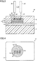
- an anti-counterfeiting structure 10 includes an allochroic layer 11, a foamable layer 12, which serves as an example of a first layer, an optical device 13, which is located between the allochroic layer 11 and the foamable layer 12 and serves as an example of a second layer, and a coating layer 14 that covers the foamable layer 12.
- the allochroic layer 11 is a layer containing an allochroic part that has a characteristic of changing from a first material to a second material in response to laser irradiation, that is, a layer containing an allochroic part that changes its color in response to laser irradiation.
- the foamable layer 12, the optical device 13, and the coating layer 14 are layers transmissible to a laser beam.
- the foamable layer 12 is a layer having a characteristic of changing, by laser irradiation, from an unfoamed, or pre-foamed, state to a foamed, or post-foamed, state. In other words, the foamable layer 12 is a layer that foams in response to laser irradiation.
- the coating layer 14 and the foamable layer 12 are words, the foamable layer 12 is a layer that foams in response to laser irradiation.
- the coating layer 14 and the foamable layer 12 are bonded together more weakly than the foamable layer 12 and the optical device 13 are.
- Such an anti-counterfeiting structure 10 makes it possible to record visible information on the allochroic layer 11 by laser irradiation of the allochroic part of the allochroic layer 11 and to cause the foamable layer 12 to foam by laser irradiation of the foamable layer 12.
- Removing the optical device 13 from the allochroic layer 11 having predetermined visible information first requires removal of the coating layer 14 from the anti-counterfeiting structure 10. While the foamable layer 12 and the optical device 13 maintain their bonding at this time, the state of the foamable layer that has been foamed in the anti-counterfeiting structure 10 is likely to be distorted by the stresses of removing the coating layer 14 from the anti-counterfeiting structure 10. Removing the coating layer 14 from the anti-counterfeiting structure 10, therefore, leaves, on the structure including the optical device 13, a trace of the coating layer 14 being removed, which in turn makes it possible to prevent counterfeiting from being carried out by removal of the optical device 13 from the anti-counterfeiting structure 10.
- the first layer is the foamable layer 12 and the second layer is the optical device 13.
- This configuration allows the optical device 13 to consume less laser beam energy during laser irradiation from the coating layer 14 toward the foamable layer 12 than a configuration in which the foamable layer 12 is sandwiched between the optical device 13 and the coating layer 14.
- the anti-counterfeiting structure 10 can be irradiated with less laser beam energy.
- the foamable layer 12 includes a foamable member 12a and a foam-promoting portion 12b.
- the foam-promoting portion 12b has a part that overlaps with a part of the foamable member 12a in a plan view of the coating layer 14.
- the foam-promoting portion 12b has a characteristic of promoting foaming in the part of the foamable member 12a by laser irradiation. This makes it possible to selectively cause foaming in the part of the foamable member 12a overlapping with the foam-promoting portion 12b.
- the foam-promoting portion 12b is constituted by a plurality of promoting members 12bl, each being located between the optical device 13 and the foamable member 12a in a thickness direction of the anti-counterfeiting structure 10. Each promoting member 12bl is located away from the other remaining promoting members 12bl in the plan view of the coating layer 14.
- the anti-counterfeiting structure 10 further includes an intermediate layer 15.
- the intermediate layer 15 is located between the optical device 13 and the foamable layer 12 in the thickness direction of the anti-counterfeiting structure 10, and fills each gap between the promoting members 12b1 in the plan view of the coating layer 14.
- the configuration in which the intermediate layer 15 fills the gap between the promoting members 12bl enhances flatness on a surface in contact with the optical device 13, so that optical characteristics of the optical device 13 will vary less within a plane parallel to the coating layer 14.
- the optical device 13 is, for example, an optically variable device (OVD) and is configured to have a fine uneven structure.
- the optical device 13 includes a forming part 13a for forming the uneven structure of the optical device 13 and an amplifying part 13b for amplifying an optical effect of the optical device 13.
- the OVD is an optical device that reproduces a different image for each direction in which the OVD is visually recognized.
- the optical device 13 is a diffraction grating, a hologram, or the like.
- the optical device 13 may be a multilayer film constituted by three or more layers.
- the optical device 13 may optionally not include the forming part 13a and the amplifying part 13b but may be only formed of a plurality of films each having a different refractive index.
- the anti-counterfeiting structure 10 further includes an adhesive layer 16 for adhering the optical device 13 to the allochroic layer 11 and a base material 17 for supporting the allochroic layer 11.
- the adhesive layer 16 is transmissible to a laser beam.
- the device structure 10D has a first surface 10D1 and a second surface 10D2, which is a surface opposite to the first surface 10D1.
- the first surface 10D1 is one surface of the foamable layer 12, and the second surface 10D2 is one surface of the adhesive layer 16.
- the first surface 10D1 and the coating layer 14 are bonded together more weakly than the second surface 10D2 and the allochroic layer 11, and more weakly in the device structure 10D than mutually adjacent layers are bonded.
- the device structure 10D removed from the allochroic layer 11 still needs to be adhered to a fake allochroic layer 11.
- Reproducing a state in a fake anti-counterfeiting structure in which the device structure 10D is sandwiched between the allochroic layer 11 and the coating layer 14 in a real anti-counterfeiting structure requires the coating layer 14 to be removed from the device structure 10D and the removed device structure 10D to be sandwiched again by the fake coating layer 14 and the fake allochroic layer 11.
- the foamable layer 12 and the optical device 13 more specifically, the foamable layer 12 and the intermediate layer 15, and the intermediate layer 15 and the optical device 13, are preferably bonded more strongly than the internal cohesive failure strength of the optical device 13.
- Such a configuration makes it impossible to separate the optical device 13 and the foamable layer 12 from each other without destroying the optical device 13 during an attempt to remove the foamable layer 12 from the optical device 13.
- the foamable layer 12 and the optical device 13 may be bonded together as strongly as or more weakly than the internal cohesive failure strength of the optical device 13. In such a configuration, a certain degree of stress still acts on the foamable layer 12 and the optical device 13 during removal of the foamable layer 12 from the optical device 13. It is thus a matter of course that the action of stress changes the foaming state in the foamable layer 12, and at least a part of the optical device 13 deforms to an extent of being unable to perform its inherent function thereof. This can prevent counterfeiting from being carried out by removal of the optical device 13 from the anti-counterfeiting structure 10.
- the foamable layer 12 overlaps with a part of the allochroic layer 11 in the plan view of the coating layer 14.
- a whole of the allochroic layer 11 opposed to the coating layer 14 in a plan view is an allochroic part.
- the foamable layer 12 has a part that overlaps with a part of the allochroic part in the plan view of the coating layer 14.
- foaming in a part of the foamable layer 12 and discoloration in a part overlapping with the part of the foamable layer 12 in the plan view of the coating layer 14 in the allochroic part can be also carried out by one occasion of laser irradiation for the purpose of discoloration.
- the laser irradiation may be carried out such that energy reaches the foam-promoting portion 12b and a part overlapping with the foam-promoting portion 12b in the plan view of the coating layer 14. Foaming in the foamable layer 12 and discoloration in the allochroic layer 11 can be thereby carried out almost simultaneously.
- the plurality of promoting members 12b1 are located on the allochroic layer 11 so as to indicate predetermined visible information.
- a part of the coating layer 14 overlapping with each promoting member 12b1 is configured to have a characteristic of changing its unfoamed state to the foamed state by laser irradiation to each promoting member 12b1.
- the part of the coating layer 14 overlapping with each promoting member 12b1 is configured to foam by the laser irradiation to each promoting member 12b1.
- the anti-counterfeiting structure 10 can thus contain visible information indicated by the allochroic part of the allochroic layer 11 and visible information indicated by the foamed part of the cover layer 14.
- the visual information indicated by the plurality of promotion parts 12b1 is a plurality of numbers consisting of numerals "1", "2", and "3". Note that the visible information may consist of letters, symbols, and figures in addition to numbers, or may consist of at least two of numbers, letters, symbols, and figures.
- the device structure 10D overlaps with a part of the allochroic layer 11, but may overlap with the whole of the allochroic layer 11.
- the optical device 13 included in the device structure 10D may extend on the whole of the allochroic layer 11, or the foaming layer 12 may extend on the whole of the allochroic layer 11.
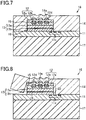
- a method of laser-irradiating the anti-counterfeiting structure 10 will be described with reference to Figs. 3 to 6 .
- a method of applying a laser beam for forming a predetermined part in the foamable layer 12 of the anti-counterfeiting structure 10 will be described first, followed by applying a laser beam for recording visible information on the allochroic layer 11 thereof.
- a part of the anti-counterfeiting structure 10 where the optical device 13 is located is dotted for schematic illustration of an image of the optical device 13 to be recognized by transmission through the coating layer 14 in the plan view of the coating layer 14.
- irradiation for recording visible information on the allochroic layer 11 may be carried out before irradiation for foaming the foamable layer 12.
- the irradiation recording visible information on the allochroic layer 11 and the irradiation for causing the foamable layer 12 to foam may be carried out almost simultaneously.
- the following description contains an example in which irradiation of the anti-counterfeiting structure 10 is performed with respect to the coating layer 14 from a side opposite to the base material 17, but the anti-counterfeiting structure 10 may be laser-irradiated from a side opposite to the coating layer 14 relative to the base material 17.
- the anti-counterfeiting structure 10 is first laser-irradiated LB in order to foam a predetermined part of the foamable layer 12.
- the foam-promoting portion 12b, of the anti-counterfeiting structure 10 included in the predetermined part and a part around the foam-promoting portion 12b thereof in the plan view of the coating layer 14 are irradiated with the laser beam LB by use of a laser 20.
- Energy of the laser beam LB emitted by the laser 20 is set to a level at which the part of the foamable member 12a that overlaps with the foam-promoting portion 12b can foam in the plan view of the coating layer 14.
- the energy of the laser beam LB is set to a level at which energy that is large enough to change an unfoamed part of the foamable member 12a to a foamed state reaches the foam-promoting portion 12b.
- the energy of the laser beam LB and a position of a focal point thereof are set so that energy that is large enough to discolor the allochroic layer 11 will not reach the allochroic layer 11.
- the whole of the part of the foamable member 12a overlapping with the foam-promoting portion 12b easily foams in the plan view of the coating layer 14.
- the irradiated part 12c including the part where the foam-promoting portion 12b is located and the part around the foam-promoting portion 12b are irradiated with the laser beam LB to cause the foamable layer 12 to foam.
- a foamed part is formed in the part of the foamable layer 12 overlapping with the foam-promoting portion 12b in the plan view of the coating layer 14 and a foamed part 14a is formed in the part of the coating layer 14 overlapping with the foam-promoting portion 12b in the plan view of the coating layer 14.
- the foamed part 14a shows visible information 18 on the observation side of the anti-counterfeiting structure 10.
- the anti-counterfeiting structure 10 is laser-irradiated to record visible information on the allochroic layer 11.
- a part of the allochroic layer 11 that overlaps with the foamable layer 12 and a part of the allochroic layer 11 that does not overlap with the foamable layer 12 in the plan view of the coating layer 14 are respectively laser-irradiated.
- the energy of the laser beam LB emitted by the laser 20 is set to a level at which energy that is large enough to discolor the allochroic layer 11 reaches the allochroic layer 11.
- the energy of the laser beam LB is set to a level at which energy that is large enough to change a first material forming the allochroic layer 11 to a second material reaches the allochroic layer 11.
- the energy level of the laser beam LB and the position of the focal point thereof are set to prevent each of the layers other than the allochroic layer 11, the layers through which the laser beam LB passes, i.e., the coating layer 14, the foamable layer 12, the optical device 13, and the layers 16, from discoloring or foaming.
- Carbonizing the first material that forms the allochroic layer 11 to provide the second material can form a discolored part in the allochroic layer 11.
- carbonization of the allochroic layer 11 caused by the laser irradiation discolors the allochroic layer 11 from a first color, or a pre-irradiated color, to a second color, or a post-irradiated color.
- the allochroic layer 11 preferably contains a material that is absorbent of the laser beam LB. A pigment is sufficient as such a material.
- the first material forming the allochroic layer 11 contains a pigment
- variation in a crystal structure of a metal ion in the pigment or a hydration amount in the metal ion crystal caused by the laser beam LB irradiation changes the first material into the second material.
- a chemical change in such a pigment forms a discolored part in the allochroic layer 11.
- a chemical change in the pigment caused by the laser irradiation discolors the allochroic layer 11 from the first color, or the pre-irradiated color, to the second color, or the post-irradiated allochroic layer color.
- the first material forming the allochroic layer 11 may contain a resin and a pigment.
- irradiating the part of the allochroic layer 11 with the laser beam LB increases a molecular density of the pigment in the irradiated part thereof, where the pigment is more concentrated than in another part of the allochroic layer 11.
- the laser-irradiated part of the allochroic layer 11 changes into the second material whose color is more dense than in the part of the allochroic layer 11 that is not irradiated with the laser beam LB.
- the condensation in the pigment caused by the laser irradiation discolors the allochroic layer 11 from a first color, or a less dense color, to a second color, or a more dense color.
- the first material forming the allochroic layer 11 may also contain a dye.
- the allochroic layer 11 contains a dye
- irradiating the part of the allochroic layer 11 with the laser beam LB decomposes and decolorizes the dye in the irradiated part thereof, compared with another part of the allochroic layer 11.
- the discolored part of the allochroic layer 11 irradiated with the laser beam LB changes into the second material whose color is less dense than in the part of the allochroic layer 11 that is not laser-irradiated.
- the decoloration of the dye caused by the laser irradiation discolors the allochroic layer 11 from the first color, a more dense color, to the second color, a less color.
- a facial image 11a and personal information 11b are recorded in the allochroic layer 11.
- a part of the facial image 11a overlaps with a part of the foamable layer 12, while none of the personal information 11b overlaps with the foamable layer 12.
- the facial image 11a is typically an image corresponding to a face of an individual to be authenticated by use of the anti-counterfeiting structure 10.
- the personal information 11b is information on an individual to be authenticated by use of the anti-counterfeiting structure 10.
- the information includes characters, numbers, and the like, but may be a predetermined graphic or the like.
- FIG. 7 in the laser-irradiated anti-counterfeiting structure 10, a part of the foamable member 12a overlapping with each promoting member 12bl in the plan view of the coating layer 14 has a foamed part 12d.
- the foamable member 12a has a plurality of foamed parts 12d, each being located apart from the remaining foamed parts 12d in the plan view of the coating layer 14.
- a part where each foamed part 12d is located protrudes away from the allochroic layer 11 in a thickness direction of the anti-counterfeiting structure 10.
- a surface of the foamable member 12a a surface that is in contact with the coating layer 14, is a stepped surface.
- a part of the coating layer 14 overlapping with the promoting member 12b1 included in the predetermined part in the plan view of the coating layer 14, has a foamed part 14a.
- the coating layer 14 has a plurality of foamed parts 14a, each being located apart from the remaining foamed parts 14a in the plan view of the coating layer 14. The location of each foamed part 14a in the coating layer 14 substantially overlaps with a position of one foamed part 12d in the foamable layer 12 in the plan view of the coating layer 14.
- a part where each foamed part 14a is located protrudes in a direction away from the allochroic layer 11 in a thickness direction of the anti-counterfeiting structure 10.
- a step is formed in a part of the coating layer 14, a part constituting a part of an outer surface of the anti-counterfeiting structure 10.
- the protruding part on the surface of the coating layer 14, or the foamed part 14a tends to attract more stress than the other parts.
- the observer of the anti-counterfeiting structure 10 can recognize the visible information 18 by touching the anti-counterfeiting structure 10.
- a discolored part 11c is formed in a part of the allochroic layer 11, a laser-irradiated part.
- the discolored part 11c forms the facial image 11a and personal information 11b described above in a plan view of the cover layer 14.
- the discolored part 11c is a part of the allochroic layer 11 and is constituted by the second material.
- a person attempting to counterfeit the anti-counterfeiting structure 10 removes the coating layer 14 from the allochroic layer 11 for the optical device 13 provided with the anti-counterfeiting structure 10, the coating layer covering the device structure 10D including the foamable layer 12 and the optical device 13.
- the coating layer 14 and the foamable layer 12 are bonded together more weakly than the foamable layer 12 and the optical device 13 are, and even more weakly than the allochroic layer 11 and the adhesive layer 16 are.
- the coating layer 14 comes off from the foaming layer 12, while the foamable layer 12 and the optical device 13 as well as the adhesive layer 16 and the allochroic layer 11 tend to remain bonded.
- the stress applied by the counterfeiter to the anti-counterfeiting structure 10 acts on the foamed part 12d, which is mechanically weaker than the other parts.
- the stress applied by the counterfeiter to the anti-counterfeiting structure 10 acts on the foamed part 14a of the coating layer 14, which is mechanically weaker than the other parts.
- the foamed part 12d of the foamable layer 12 assumes a state that is different from what it was before the counterfeiter removed the coating layer 14 from the foamable layer 12. This forms a deformable part 12e as a trace of the coating layer 14 being removed from the foamable layer 12 in a part where the foamed part 12d was located before the coating layer 14 was removed from the foamable layer 12.
- the deformable part 12e of the foamable layer 12 is a crushed part of the foamed part 12d and a part where the foamed part 12d has deformed from what it was shaped as before the coating layer 14 was removed from the foamable layer 12, the crushing being due to discharge of bubbles retained between the foamed part 12d and the foam-promoting portion 12b to an outside of the foamable member 12a.
- the foamed part 14a of the coating layer 14 assumes a state that is different from what it was before the counterfeiterrr removed the coating layer 14 from the foamable layer 12. This forms a deformable part 14b as a trace of the coating layer 14 being removed from the foamable layer 12 in a part where the foamed part 14a was located before the coating layer 14 is removed from the foamable layer 12.
- the deformable part 14b of the foamable layer 14 is a crushed part of the foamed part 14a and a part where the foamed part 14a has deformed from the shape before the coating layer 14 was removed from the foamable layer 12, the crushing being due to discharge of bubbles retained between the foamed part 14a and the foamable member 12a to an outside of the coating layer 14.
- the deformable part 12e is formed in the foamable layer 12.
- the anti-counterfeiting structure inevitably includes the device structure 10D having a trace indicating that the device structure 10D has been removed from a genuine anti-counterfeiting structure 10. This can prevent counterfeiting of the anti-counterfeiting structure 10 from being carried out by removal of the optical device 13 from the anti-counterfeiting structure 10.
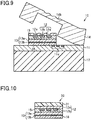
- FIG. 10 shows a part of a cross-sectional structure of the transfer foil for convenience of illustration.
- a transfer foil 30 includes a support layer 31.
- the foamable layer 12, the intermediate layer 15, the optical device 13, and the adhesive layer 16 are stacked on a surface of the support layer 31 in the stated order.
- a first step to form the transfer foil 30 is to prepare the support layer 31.
- the support layer 31 may have heat resistance against heat applied to the support layer 31 during a course of forming the transfer foil 30 and mechanical strength that can withstand a force applied to the support layer 31 during a course of forming the transfer foil 30.
- the material of the support layer 31 may be a synthetic resin, a natural resin, paper, or synthetic paper.
- the support layer 31 may have a single-layer structure constituted by one of the layers formed by the respective forming materials or may have a multilayer structure constituted by two or more thereof.
- suitable forming materials include polyvinyl chloride, polyester, polycarbonate, polymethyl methacrylate, polystyrene, polyethylene, polyethylene terephthalate, polyethylene naphthalate, polypropylene, and polyvinyl alcohol.
- the support layer 31 is preferably approximately 25 ⁇ m or more to 50 ⁇ m or less thick in terms of operability and processability thereof.
- a foamable member 12a constituting the foamable layer 12 is then formed on one surface of the support layer 31.
- the foamable member 12a also acts as a peelable layer configured to enable removal of the support layer 31 from another layer stacked on the support layer 31 of the transfer foil 30.
- the foamable member 12a is a member that foams when it is laser-irradiated.
- the foamable member 12a is configured such that the material that forms the foamable member 12a decomposes to generate a gas, for example, when the foamable member 12a warms up until it reaches a predetermined temperature.
- the foamable member 12a may only be transmissible to a laser beam and be able to withstand a thermal pressure applied to the foamable member 12a when the transfer foil 30 is thermally transferred.
- the foamable member 12a can be formed of a resin, specifically a thermoplastic resin, a thermosetting resin, an ultraviolet curable resin, or an electron beam curable resin.
- thermoplastic resins include a polycarbonate resin, a polyether imide resin, a cyclic polyolefin copolymer, a modified norbornene resin, a polyamide imide resin, a polyimide resin, and a nitrocellulose resin.
- the foam-promoting portion 12b is formed on a surface of the foamable member 12a opposite to a surface which is in contact with the support layer 31.
- one promoting member 12bl forms a plurality of promoting members 12bl on the surface of the foamable member 12a opposite to the surface in contact with the support layer 31 so as to be away from the other promoting members 12b1 in a plan view of the support layer 31.
- the foam-promoting portion 12b may be configured to cause the foamable member 12a to foam when it is laser-irradiated, the foamable member 12a being in contact the foam-promoting portion 12b.
- the foam-promoting portion 12b may be configured to have a characteristic of promoting an unfoamed part of the foamable member 12a to assume a foamed state, the part being in contact with the foam-promoting portion 12b.
- the foam-promoting portion 12b has, for example, a function of increasing energy of the laser beam applied to the foam-promoting portion 12b, applying to the foamable member 12a more energy than in a state in which the foamable member 12a is not in contact with the foam-promoting portion 12b.
- the foam-promoting portion 12b thus heats the foamable member 12a to a temperature higher than it heats the foamable member 12a when the foamable member 12a is laser-irradiated with the foamable member 12a being not in contact with the foam-promoting portion 12b, and decomposes a part of the foamable member 12a.
- Decomposing the foamable member 12a produces carbon- or oxygen-containing gas constituting the foamable member 12a because the foamable member 12a is formed of various resins as described above.
- the foam-promoting portion 12b can be formed of an ink that scatters infrared light having a 1064-nm wavelength, a reflective ink, or an absorbent ink.
- the ink reflecting the infrared light having the 1064-nm wavelength may be an ink containing a pearl pigment. Note that the infrared light having a 1064-nm wavelength is used during laser printing, that is, when visible information is recorded on the allochroic layer 11 by use of a laser.
- a pigment-containing ink may be used as the ink that scatters infrared light.
- a particle of a compound can be used as the pigment, and an inorganic compound can be used as the particle of the compound.
- the inorganic compound may be titanium oxide, silica, or alumina.
- the ink that absorbs the infrared light having the 1064-nm wavelength may be a polymer having a molecular bond that absorbs the infrared light having the 1064-nm wavelength.
- the pearl pigment typically includes a core part formed of mica and a coating part covering the core part.
- the coating part may be formed of any material that makes the mica reflective.
- the material may assume a transparent color in a visible region and may be metal oxide, metal sulfide, metal selenide, and metal chloride or other material having a refractive index of 2.0 or greater.
- An inorganic compound can be used to form the coating part.
- Suitable inorganic compounds include Sb 2 S 3 , Fe 2 O 3 , PbO, ZnSe, CdS, Bi 2 O 3 , TiO 2 , PbCl 2 , CeO 2 , Ta 2 O 5 , ZnS, ZnO, CdO, Nd 2 O 3 , Sb 2 O 3 , SiO, and In 2 O 3 .
- the coating part may have a single-layer structure constituted by one of the layers formed by the respective forming materials or may have a multilayer structure constituted by two or more thereof.
- the pearl pigment incidentally, has an effect of promoting laser marking of a resin, that is, discoloration of the resin.
- the pearl pigment is recognized to have a function of enabling a polyolefin resin to discolor when the pearl pigment is added to a polyolefin resin and other material that do not discolor even when it is laser-irradiated.
- the mica forming the core part of the pearl pigment sensitizes a reaction in the resin caused by the laser beam.
- the core and coating parts constituting the pearl pigment have a function of absorbing the laser beam to make the resin that is in contact with the pearl pigment warmer than when these parts are laser-irradiated in a state in which the pearl pigment is not in contact the resin. This allows decomposition of the resin to form carbon in the resin with a result that the generated carbon is recognized as a black discolored part. Note that, in a configuration where the coating part contains TiO 2 or the resin contains TiO 2 , the laser irradiation produces black low-order titanium oxide.
- the pearl pigment in a circumstance where there is a difference in refractive index by more than 0.4 between the core part and the coating part, the pearl pigment is highly reflective to white light incident thereon and is birefringent at an interface between the core part and the coating part.
- the pearl pigment can thus reflect rainbow-colored light.
- the pearl pigment to be used to form the foam-promoting portion 12b has only to have a function of causing the foamable member 12a to foam.
- the pearl pigment therefore may be one that reflects the rainbow-colored light, or may be one that reflects bicolored light.
- the pearl pigment may assume a spherical shape, a scaly shape, and other shape.
- a pearl pigment having a spherical particle is preferably around 1 ⁇ m or more to 50 ⁇ m or less on average in diameter, more preferably around 1 ⁇ m or more to 15 ⁇ m or less.
- the intermediate layer 15 of the foamable member 12a is formed to fill a gap between the foam-promoting portions 12b in the plan view of the support layer 31 on a side opposite to a side that is in contact with the support layer 31 and to cover the foam-promoting portions 12b in a thickness direction of the foamable member 12a.
- the intermediate layer 15 is preferably formed of a resin that protects the foam-promoting portion 12b and is heat-resistant to an extent that does not inhibit the optical device 13 from being formed.
- the intermediate layer 15 may be formed of any of a thermoplastic resin, a thermosetting resin, an ultraviolet curable resin, and an electron beam curable resin.
- the intermediate layer 15 may be preferably formed of a polyester resin, a polycarbonate resin, a polyarylate resin, a polysulfone resin, a polyethersulfone resin, a polyetherimide resin, a cyclic polyolefin copolymers, modified norbornene resin, a polyamideimide resin, a nitrocellulose resin, or the like.
- Particles are preferably added to the resin material forming the intermediate layer 15.
- the particle preferably has a diameter smaller than or equal to the pigment present in the foam-promoting portion 12b, preferably 1 ⁇ m or more to 30 ⁇ m or less.
- the material that forms the intermediate layer 15 contains a particle with a diameter less than or equal to the diameter of the pigment particle, a particle in the forming material easily falls into a gap formed between the promoting members 12b1.
- the gap formed between the promoting members 12bl is filled more easily with the material that forms the intermediate layer 15. This facilitates protection of a shape of each promoting member 12b1 by the intermediate layer 15, compared with a configuration in which the gap is formed between the respective promoting members 12b1.
- the particle may be formed of either an organic material or an inorganic material.
- suitable particles may be of Teflon powder (Teflon is registered trademark), a polyethylene powder, a silicone-based fine particle, or an acrylonitrile-based fine particle.
- Teflon is registered trademark
- the particle may be, for example, a silica particle.
- An amount of the particles in the material that forms the intermediate layer 15 may be determined by a color tone required of the intermediate layer 15, transparency, and marking efficiency required of part of the allochroic layer 11 overlapping with the intermediate layer 15 in the plan view of the coating layer 14, that is, a degree of discoloration relative to energy applied to the allochroic layer 11.
- the amount of the particles is preferably 0.05 wt% or more to 50 wt% or less relative to the resin described above, and more preferably 0.5 wt% or more to 20 wt% or less.
- the optical device 13 is formed on a surface of the intermediate layer 15, a surface opposite to a surface in contact with the foamable layer 12.
- the optical device 13 is preferably an OVD.
- the OVD is an optical device that reproduces a different image when a visual direction of the OVD changes to another direction.
- Examples of the OVD include a hologram, a diffraction grating, and a multilayer film.
- the hologram and the diffraction grating may each be of a relief type, which records an interference fringe of light as a fine uneven pattern on a plane or of a volume type, which records the interference fringe in a thickness direction of the optical device 13.
- the optical device 13 is a relief-type hologram or a relief-type diffraction grating
- the optical device 13 has a forming part 13a and an amplifying part 13b, the forming part 13a having a relief surface with a fine uneven pattern, and the amplifying part 13b covering a relief surface of the forming part 13a.
- the first step in forming the relief-type hologram or relief-type diffraction grating is to form a master plate of the relief surface having the fine uneven pattern, and then form a nickel press plate having a reproduction of the uneven pattern of the master plate by an electroplating method.
- the next step is to form a coating film for forming the forming part 13a on the surface of the intermediate layer 15 opposite to the surface in contact with the foamable layer 12 before forming a forming part 13a having the relief surface by curing the coating film with the press plate being pressed against the coating film.
- the following step is to form the amplifying part 13b for enhancing a diffraction efficiency in the relief-type hologram or the relief-type diffraction grating on at least a part of the relief surface of the forming part 13a.
- the forming part 13a may be a layer where the relief surface is formed by the press plate being pressed thereagainst, and may be formed of an ultraviolet curable resin, a thermosetting resin, a thermoplastic resin, or an electron beam curable resin, etc., more specifically, epoxy (meth)acrylic or urethane (meth)acrylate.
- the forming part 13a may have a single-layer structure constituted by only one of the layers formed by the respective forming resins described above or may have a multilayer structure constituted by two or more thereof.
- the forming part 13a may be formed not only of the materials described above, but of a material having a relief surface, a material that is capable of forming a layer configured to reproduce a different image when a visual direction of the optical device 13 changes to another direction.
- the forming part 13a may be formed by a photopolymer method.
- the forming part 13a can be formed of a monomer, an oligomer, or a polymer having an ethylenic unsaturated bond or an ethylenically unsaturated group.
- Suitable monomers include 1,6-hexanediol, neopentyl glycol diacrylate, trimethylolpropane triacrylate, pentaerythritol triacrylate, pentaerythritol tetraacrylate, dipentaerythritol pentaacrylate, and dipentaerythritol hexaacrylate.
- Suitable oligomers include epoxy acrylate, urethane acrylate, and polyester acrylate.
- Suitable polymers include a urethane-modified acrylic resin and an epoxy-modified acrylic resin.
- the monomer, oligomer, and polymer having the ethylenically unsaturated bond or the ethylenically unsaturated group may be used in mixture of two or more of the materials listed above.
- the monomers, the oligomers, and the polymers can be mutually crosslinked by imparting in advance a reactive group that undergoes a crosslinking reaction to the monomers, oligomers and polymers listed above and by use of an isothiocyanate compound, a silane coupling agent, an organic titanate crosslinking agent, an organic zirconium crosslinking agent, or organic aluminate.
- the monomer, oligomer, and polymer having the ethylenically unsaturated bond or the ethylenically unsaturated group may be used in mixture with another resin.
- the monomer and other component can be crosslinked with a skeleton of another resin by imparting in advance a reactive group that undergoes a crosslinking reaction to the monomers, oligomers and polymers listed above and by use of, for example, an isothiocyanate compound, a silane coupling agent, an organic titanate crosslinking agent, an organic zirconium crosslinking agent, or organic aluminate.
- Such a method makes it possible to obtain the polymers having the ethylenically unsaturated bond or the ethylenically unsaturated group. These polymers provide high moldability of the relief surface and are less liable to stain the press block because they are solid at normal temperature and are less tacky.
- the forming part 13a can be formed of monomers, oligomers and polymers having an epoxy group, oxetane skeleton-containing compounds and vinyl ethers.
- a photopolymerization initiator may be added to the electron beam curable resin.
- Suitable photopolymerization initiators include photoradical polymerization initiators, photocationic polymerization initiators, and a combination type of photoradical polymerization initiator and photocationic polymerization initiator, or of a hybrid type, depending on the resin to which the photopolymerization initiator is added.
- Suitable photoradical polymerization initiators include benzoin compounds, anthraquinone compounds, phenyl ketone compounds, benzil dimethyl ketal, thioxanthone, acylphosphine oxide, and Michler's ketone.
- the benzoin compounds include benzoin, benzoin methyl ether and benzoin ethyl ether.
- the anthraquinone compounds include anthraquinone and methylanthraquinone.
- the phenyl ketone compounds include acetophenone, diethoxyacetophenone, benzophenone, hydroxyacetophenone, 1-hydroxycyclohexyl phenyl ketone, ⁇ -aminoacetophenone and 2-methyl-1-(4-methylthiophenyl)-2-morpholinopropane-1-one.
- the photocationic polymerization initiator may be an aromatic diazonium salt, an aromatic iodonium salt, an aromatic sulfonium salt, an aromatic phosphonium salt, a mixed ligand metal salt, or the like.
- the hybrid type photopolymerization initiator may be a photopolymerization initiator prepared by mixing the photoradical polymerization initiator and the photocationic polymerization initiator, or may be a photopolymerization initiator that is capable of initiating both the photopolymerization and the photocationic polymerization.
- Suitable photopolymerization initiators that are capable of initiating both the photoradical polymerization and the photocationic polymerization include an aromatic iodonium salt and an aromatic sulfonium salt.
- a blending amount of the photopolymerization initiator relative to the electron beam curable resin may be determined according to the electron beam curable resin and the photopolymerization initiator.
- the photopolymerization initiator is preferably added at a ratio between 0.1 wt% or more and 15 wt% or less to the electron beam curable resin.
- a sensitizing dye may be added to a mixture containing the electron beam curable resin and the photopolymerization initiator. Still further, a dye, a pigment, various additives, a crosslinking agent, etc. may be added as necessary. In order to improve the moldability of the forming part 13a, a resin nonreactive to the photopolymerization reaction may be added.
- Examples of the various additive include a polymerization inhibitor, a leveling agent, a defoaming agent, an anti-fouling agent, an adhesion improving agent, a coating surface modifying agent, a plasticizer, and a nitrogen-containing compound.
- An exemplary crosslinking agent is an epoxy resin.
- the nonreactive resin may be the thermoplastic resin or thermosetting resin listed above.
- the amplifying part 13b is a part configured to enhance the diffraction efficiency on the relief surface of the forming part 13a, and is formed of a material having a different refractive index from the resin forming the relief surface, that is, a polymeric material.
- the amplifying part 13b may be formed of a dielectric material such as TiO 2 , Si 2 O 3 , SiO, Fe 2 O 3 , and ZnS, or of a metallic material such as Sn, Cr, Ni, Cu, and Au.
- the amplifying part 13b may have a single-layer structure constituted by only one of the layers formed by the respective forming materials listed above or may have a multilayer structure constituted by two or more thereof.
- the amplifying part 13b can be formed by a vacuum deposition method, a sputtering method, and other method.
- the thickness of the amplifying part 13b is approximately 50 ⁇ or more to 10000 ⁇ or less according to a function required thereof.
- the amplifying part 13b may be formed on the whole relief surface of the forming section 13a, but may be formed on a part of the relief surface. Forming the amplifying part 13b on the part of the relief surface follows the steps of: printing an ink containing a water-soluble resin on the part of the relief surface where the amplifying part 13b is not to be formed; forming a film for forming the amplifying part 13b on the whole relief surface; and washing the water-soluble resin to remove the film formed on a part overlapping with the water-soluble resin in the thickness direction of the optical device 13.
- the amplifying part 13b can be also formed in a part of the relief surface in the steps of: forming a film for forming the amplifying part 13b on the whole relief surface; forming a mask in an area on the relief surface for the amplifying part 13b, the area being part of the film; and exposing the film to an alkaline or acidic chemical that dissolves the film to remove the part of the amplifying part 13b.
- a laser is another method such as a laser removing method to remove the part of the film for forming the amplifying part 13b.
- the amplifying part 13b on a part of the relief surface makes it possible for the anti-counterfeiting structure 10 having the optical device 13 to represent predetermined visible information formed by the amplifying part 13b, which can in turn provide a better design of the anti-counterfeiting structure 10.
- the adhesive layer 16 is formed of a material that is cured by irradiation with ultraviolet rays or an electron beam
- the amplifying part 13b is formed of a material that allows substantially no transmission of the ultraviolet rays and the electron beam
- forming the amplifying part 13b on the part of the relief surface can provide the following effects.
- emitting ultraviolet rays or an electron beam from the foamable layer 12 toward the adhesive layer 16 does not irradiate the part overlapping with the amplifying part 13b in a plan view of the optical device 13, but does irradiate the part not overlapping with the amplifying part 13b.
- the part of the adhesive layer 16 irradiated with the ultraviolet rays or the electron beam is cured, while the unirradiated part is not cured.
- the cured part of the adhesive layer 16 is hardly removed from the allochroic layer 11, whereas the uncured part is easily removed therefrom.
- Part of the device structure 10D is consequently easily broken by a force applied thereto during the removal of the device structure 10D from the color change layer 11.
- the optical device 13 is a multilayer film formed from a plurality of thin films, a multilayer film that causes the optical device 13 to present a different image color in response to a change in the visual direction thereof, the optical device 13 is constituted as described below.
- the optical device 13 is a multilayer film constituted by a plurality of layers each having a different optical characteristic.
- a material with a refractive index over approximately 1.5 and below 2 is referred to as a low refractive index material, while a material with a refractive index of 2 or greater is referred to as a high refractive index material.
- a layer formed of a high refractive index material is referred to as a high refractive index layer, while a layer formed of a low refractive index material is referred to as a low refractive index layer.
- a multilayer film including both a low refractive index layer and a high refractive index layer may be a structure of two or more high refractive index layers and one low refractive index layer alternately stacked.
- Each layer of the multilayer film may be formed of the materials shown in the following Table 1.
- Table 1 Material Refractive index (n) Material Refractive index (n) Sb 2 S 3 3.0 SiO 2.0 Fe 2 O 3 2.7 Si 2 O 3 2.5 TiO 2 2.6 In 2 O 3 2.0 CdS 2.6 PbO 2.6 CeO 2 2.3 Ta 2 O 3 2.4 ZnS 2.3 ZnO 2 2.1 PbCl 2 2.3 ZrO 2 2.0 CdO 2.2 Cd 2 O 3 1.8 Sb 2 O 3 2.0 WO 3 2.0
- layers constituting the multilayer film may be formed solely of Fe, Mg, Zn, Au, Ag, Cr, Ni, and Cu, and other metal or of an alloy containing at least two of these, or may be formed of Si.
- the layers constituting the multilayer film may be also formed of an organic polymer with a low refractive index, including polyethylene, polypropylene, polytetrafluoroethylene, polymethyl methacrylate, and polystyrene.
- the refractive indexes of these materials are: 1.51 for polyethylene, 1.49 for polypropylene, 1.35 for polytetrafluoroethylene, 1.49 for polymethyl methacrylate, and 1.60 for polystyrene.
- a layer formed of these organic polymers is a low refractive index layer.
- the multilayer film may have a structure in which at least one layer with a predetermined thickness selected from the high refractive index layer described above and a metal layer with a light transmittance between 30% or more and 60% or less and at least one layer with a predetermined thickness selected from low refractive index layers are alternately stacked.
- a multilayer film with such a structure can be configured to have a characteristic of absorbing or reflecting visible light having a predetermined wavelength.
- Each layer of the multilayer film may be formed of a material selected from the above materials according to optical characteristics such as refractive index, reflectance, and transmittance, weather resistance, interlayer adhesiveness. etc.
- the adhesive layer 16 is formed overall on a surface of the optical device 13 opposite to a surface which is in contact with the intermediate layer 15.
- the adhesive layer 16 is a layer for fixing a structure constituted by the support layer 31, the foamable layer 12, the intermediate layer 15, and the optical device 13 to the allochroic layer 11.
- the adhesive layer 16 is preferably formed of a pressure sensitive material, that is, a resin that exhibits adhesion to the allochroic layer 11 by application of pressure to the adhesive layer 16.
- a thermoplastic resin can be used to form the adhesive layer 16.
- An acrylic resin, a vinyl chloride-vinyl acetate copolymer, an epoxy resin, and an ethylene-vinyl acetate copolymer (EVA) are suitable as the thermoplastic resin.
- the adhesive layer 16 may be formed by use of a gravure coater, a micro gravure coater, a roll coater, and the like.
- the transfer foil 30 to be used for manufacturing the anti-counterfeiting structure 10 is thereby formed.
- the first step to manufacture the anti-counterfeiting structure 10 by use of the transfer foil 30 is to prepare the allochroic layer 11.
- the allochroic layer 11 may be configured to exhibit, in response to laser irradiation, a color different from that before being irradiated. In other words, the allochroic layer 11 may have a characteristic of changing a first material thereof to a second material in response to laser irradiation.
- the allochroic layer 11 may be formed of an inorganic material, a metallic material, an organic material, and a polymer material.
- the allochroic layer 11 is preferably formed of a material having a characteristic of starting discoloration when it is laser-irradiated with a predetermined or higher level of intensity, that is, having a threshold of the intensity of the laser beam.
- the allochroic layer 11 may be formed of a material that is capable of absorbing laser pulse energy, carbonizing at a temperature equal to or higher than a predetermined temperature, and recording information.
- Such materials are a material containing polycarbonate as a main component and a material containing polyester as a main component.
- the allochroic layer 11 may be also formed of a mixture organized to develop color by laser irradiation.
- the mixture may be a mixture of a black color-developing layer and a color-developing layer.
- a mixture containing a thermally responsive microcapsule is preferable in requiring a low level of energy for coloring the allochroic layer 11, compared with a mixture containing no thermoresponsive microcapsules.
- the allochroic layer 11 may be also formed of a mixture organized to develop color by laser irradiation.
- the mixture can contain an allochroic compound that discolors by laser irradiation and a photosensitive resin.
- the photosensitive resin include an ultraviolet curable resin and an electron beam curable resin.
- such a mixture includes a promoting compound that promotes modification of the discolored compound by laser irradiation, or bonds the promoting compound to a skeleton of the photosensitive resin for convenience of control over a threshold temperature at which the mixture discolors.
- the allochroic layer 11 may be also formed of a synthetic resin containing an additive.
- the additive may be at least one of a synthetic resin modified by laser irradiation, an inorganic material that promotes the modification of a synthetic resin as a main component by laser irradiation, a synthetic resin that contains an organic material, and an inorganic material that absorbs a laser beam and produces heat.
- the allochroic layer 11 may be formed of a mixture containing a transparent resin and at least one of a light-absorbent material and a thermosensitive coloring material.
- the allochroic layer 11 may be formed as a film formed by use of the materials for forming the allochroic layer 11 listed above.
- the allochroic layer 11 may be formed by wet-coating on a surface of another layer a coating liquid produced by dissolving in a solution the material that forms the allochroic layer 11 or a coating liquid dispersed in a liquid.
- the allochroic layer 11 may be also formed on one surface of another layer by a dry coating method such as vacuum deposition and sputtering.
- the transfer foil 30 is transferred to a part of the allochroic layer 11 in the plan view of the allochroic layer 11 in a state such that the adhesive layer 16 of the transfer foil 30 maintains contact with the allochroic layer 11.
- the transfer foil 30 may be spot-transferred to the allochroic layer 11 by a vertical stamping method, or transferred thereto by a roll transfer method.
- the first step of transferring the transfer foil 30 to the allochroic layer 11 by use of the vertical stamping method is to overlap the transfer foil 30 with one side of the allochroic layer 11 in a state such that the adhesive layer 16 of the transfer foil 30 faces the allochroic layer 11.
- the next step is to press a heated hot stamp H against the support layer 31 of the transfer foil 30. This softens a part of the adhesive layer 16 overlapping with the hot stamp H in a plan view of the allochroic layer 11 and adheres the softened part to the allochroic layer 11.
- a position of the transfer foil 30 relative to the allochroic layer 11 is changed from a relative position when a part of the transfer foil 30 is adhered. This removes the support layer 31 from the foamable member 12a at the part of the transfer foil 30 to which the adhesive layer 16 is adhered, and consequently transfers the part of the transfer foil 30 to the allochroic layer 11.
- the subsequent step is to prepare a base material 17.
- the base material 17 is preferably formed of polycarbonate (PC).
- the base material 17 is also preferably formed of polyethylene terephthalate (PET), thermoplastic polyester having noncrystalline property (PETG), polyvinyl chloride (PVC), or an ABS resin.
- the base material 17 may have a single-layer structure constituted by one of the layers formed by the respective resins listed above or may have a multilayer structure constituted by two or more thereof.
- the base material 17 may be attached to one surface of the allochroic layer 11 before a part of the transfer foil 30 is transferred to the allochroic layer 11.
- the allochroic layer 11 may be formed on one surface of the base material 17.
- the next step is to prepare the coating layer 14.
- the allochroic layer 11 to which the device structure 10D has been transferred is then sandwiched between the base material 17 and the coating layer 14, to laminate the base material 17, the coating layer 14, and the allochroic 11.
- the coating layer 14 may be formed by application of a coating liquid that contains a material that forms the coating layer 14 on the surface of the allochroic layer 11 to which the device structure 10D has been transferred.
- the coating layer 14 may be configured to be transmissible to a laser beam.
- the coating layer 14 preferably has a 60% or more to 100% or less transmittance to the light present in the visible light region, more preferably an 80% or more to 100% or less transmittance.
- the coating layer 14 is a layer that foams in response to laser irradiation.
- the coating layer 14 has a function of decomposing the material forming the coating layer 14 and generating gas when the coating layer 14 reaches a predetermined or higher temperature.
- the coating layer 14 is formed of a light-transmissible resin.
- Suitable light-transmissible resins include polycarbonate (PC), plant-derived polycarbonate (bio PC), polyethylene terephthalate (PET), polysiloxane 1,4-dimethyl phthalate (PCT), polystyrene (PS), polymethyl methacrylate (PMMA), transparent acrylonitrile butadiene styrene copolymerized synthetic resin (MABS), polyvinyl chloride (PVC), polypropylene (PP), and polyethylene (PE) polyacetal.
- PC polycarbonate
- bio PC bio PC
- PET polyethylene terephthalate
- PCT polysiloxane 1,4-dimethyl phthalate
- PS polystyrene
- PMMA polymethyl methacrylate
- MABS transparent acrylonitrile butadiene styrene copolymerized synthetic resin
- PVC polyvinyl chloride
- PP polypropylene
- the coating layer 14 may be configured to absorb, reflect, or scatter the laser beam applied to the coating layer 14 as long as it is transmissible to the laser beam and is configured to foam in response to laser irradiation.
- the coating layer 14 is configured to absorb a part of the laser beam emitted onto it, the following effect can be achieved in a part where the allochroic layer 11 and the coating layer 14 are in contact with each other during laser irradiation for discoloring the allochroic layer 11 from the substrate 17 toward the allochroic layer 11.
- the coating layer 14 absorbs parts of the laser beam emitted onto the allochroic layer 11 that have passed through the coating layer 14 without being absorbed by the allochroic layer 11. Then the part of the coating layer 14 that has absorbed the laser beam produces heat, and a part of the heat is transmitted to the allochroic layer 11. This can facilitate discoloration of a part of the allochroic layer 11.
- the allochroic part of the allochroic layer 11 and the coating layer 14 are preferably in direct contact with each other.
- the light-absorbent coating layer 14 may be formed of the light-transmissible resin listed above to which the light-absorbent material is added or have a configuration in which a light-absorbent material is applied to the surface of the coating layer 14 which is in contact with the allochroic layer 11.
- Suitable light-absorbent materials include a polyvalent metal hydroxide, an organic aluminum compound, salts such as nitrate, silicate, phosphate, oxalate, aluminum salt, and other salt, and a colorant material such as a cyanine colorant, a phthalocyanine colorant, a diimmonium colorant, an anthraquinone colorant, and an aluminum colorant.
- An amount of the light-absorbent material to be added to the light-transmissible resin may be determined depending on a wavelength of the laser beam applied to the coating layer 14, the light-transmissible resin, and the light-absorbent material.
- the amount to be added may be selected depending on an absorption efficiency relative to a laser beam energy, the light transmittance of the coating layer 14, an influence on other layers of the anti-counterfeiting structure 10, and other factors.
- the coating layer 14 is light-absorbent, the coating layer 14 is preferably 10 ⁇ m or more to 1000 ⁇ m or less thick.
- the coating layer 14 When the coating layer 14 is configured to scatter the laser beam emitted onto it, the following effect can be achieved in a part where the allochroic layer 11 and the coating layer 14 are in contact with each other during laser irradiation for discoloring the allochroic layer 11 from the substrate 17 toward the allochroic layer 11.
- the coating layer 14 reflects or scatters parts of the laser beam emitted onto the allochroic layer 11 that have passed through the coating layer 14 without being absorbed by the allochroic layer 11. At least a part of the light reflected or scattered by the coating layer 14 thus irradiates the allochroic layer 11 again.
- the allochroic layer 11 therefore absorbs the laser beam more efficiently.
- the coating layer 14 is formed of a multilayer film and a metal oxide film configured to selectively reflect light with the wavelength of the laser beam emitted to the coating layer 14.
- the multilayer film consists of a plurality of layers selected from a metal layer formed of a metal and a dielectric layer.
- the multilayer film can be formed on one surface of the base material 17 by a vapor deposition method, a sputtering method, and other methods.
- the multilayer film formed into a film shape can be bonded to the base material 17.
- the light-reflective coating layer 14 is preferably 5 nm or more to 1000 nm or less thick.
- the coating layer 14 is preferably formed of indium oxide that is highly reflective to infrared light.
- the coating layer 14 may have a multilayer structure in which an indium oxide layer, a metal layer, and a metal oxide layer are stacked, or may be a titanium oxide layer having an oxygen-deficient anatase structure. The coating layer 14 is still highly reflective to infrared light even if it has such a configuration.
- the coating layer 14 may have a configuration in which a surface in contact with the allochroic layer 11 is made rougher.
- the coating layer 14 may have a configuration in which a material that reflects light with a wavelength of a laser beam emitted to the anti-counterfeiting structure 10 is dispersed in the light-transmissible resins listed above.
- the light-reflective material include a crushed piece of material for the light-reflective coating layer 14 and a particle whose refractive index to light in a wavelength range of the laser beam is different from that of a light-transmissible resin.
- the refractive index to light in the wavelength range of the laser beam is preferably different by 0.3 or more between the light-transmissible resin and the particle.
- the personal information 11b recorded in the anti-counterfeiting structure 10 by laser irradiation may include at least one of biological information and non-biological information.
- the biometric information is a characteristic unique to an individual, a characteristic authenticated among biometric features.
- the information typically includes an image or pattern of a face, a fingerprint, and a vein pattern.
- the non-biometric information is personal information other than the biometric information.
- the non-biometric personal information typically includes one's name, date of birth, age, blood type, sex, nationality, address, domicile, telephone number, department name, and job title.
- the laser 20 described above is a far-infrared laser including a CO 2 laser, a near-infrared pulse laser including an Nd:YAG laser and an Nd:YVO laser, a pulsed laser of visible light, an excimer laser, etc.
- the laser 20 may also be an ultraviolet laser by use of a third harmonic of an Nd:YAG laser or an Nd:YVO laser, a semiconductor laser, a femtosecond laser, a picosecond laser, etc.
- the laser by use of the third harmonic of the Nd:YAG laser or the Nd:YVO laser is preferable in that it has high resolution and that the allochroic layer 11 is highly absorbent to a laser beam because the wavelength of the laser beam is included in the ultraviolet range.
- a ultrashort pulse laser such as a femtosecond laser and a picosecond laser can cut molecular bonds constituting the allochroic layer 11 in a state in which the laser-irradiated allochroic layer 11 remains cool. This makes it possible to record visible information on the allochroic layer 11 in a state in which substantially no heat is applied to the allochroic layer 11.
- YAG lasers and semiconductor lasers are preferable in being capable of serving as a small device that emits a large amount of thermal energy, and in being capable of recording visible information on the allochroic layer 11 on demand.
- a 25- ⁇ m-thick transparent polyethylene terephthalate (PET) film was prepared as a support layer for the transfer foil. Then an ink for a foamable member with the following composition was applied onto one side of the support layer to form a coating film. The coating film was then dried at 120°C for 45 seconds to form a foamable member having a thickness of 1 ⁇ m.
- PET transparent polyethylene terephthalate
- An ink for a foam-promoting portion with the following composition was subsequently printed on a surface of the foamable member opposite to a surface in contact with the support layer by a screen printing method.
- a foam-promoting member constituting the foam-promoting portion in a plan view of the supporting layer, a foam-promoting portion showing numeral "1", a foam-promoting portion representing a numeral "2", and a foam-promoting portion representing a numeral "3" were formed so that these parts would have a thickness of 5 ⁇ m after being dried.
- a coating film was formed by application of an ink for an intermediate layer, an ink with the following composition, such that the coating film covers a part where the foam-promoting portion was not located, a part being present on a surface of the foaming part where the foam-promoting portion was located, and the foam-promoting portion. Then the coating film was dried at 120°C for 45 seconds to form an intermediate layer having a thickness of 5 ⁇ m. Note that the thickness of the intermediate layer is defined as a distance between a surface opposite to the surface in contact with the foamable member in the foam-promoting portion and a surface of the intermediate layer opposite to the foaming part relative to the foam-promoting portion.
- An ink for a forming part with the following composition was applied onto the surface of the intermediate layer opposite to the surface in contact with the foamable member.
- the coating film was then dried at 120°C for 45 seconds and was 3 ⁇ m thick.
- a surface opposite to the surface in contact with the intermediate layer of the dried coating film was irradiated with ultraviolet rays while a press plate was pressed by a roll embossing method thereagainst.
- a formed part with a relief surface having a fine uneven pattern was thus formed on the surface opposite to the surface in contact with the intermediate layer.
- a 1000- ⁇ -thick zinc sulfide film was subsequently formed as a light-reflective amplifying part on the relief surface of the formed part by a vacuum evaporation method.
- An ink for an adhesive layer with the following composition was applied onto a surface of the amplifying part opposite to a surface in contact with the formed part to form a coating film that serves as an adhesive layer that would be 2 ⁇ m thick after the coating film was dried.
- the transfer foil for forming the anti-counterfeiting structure of Example 1 was produced.
- a 400- ⁇ m-thick base material and a 125- ⁇ m-thick coating layer (Makrofol ID 6-2_000000 manufactured by Bayer) were prepared.
- the base material, the allochroic layer, and the coating layer were then laminated under a condition of 190°C and 100 kgf/cm 2 for 3 minutes by use of a hydraulic molding machine in a state in which the allochroic layer having a device structure transferred was sandwiched between the base material and the coating layer.
- the base material, the allochroic layer, and the coating layer were further laminated under a condition of 25°C and 100 kgf/cm 2 for 3 minutes.
- the anti-counterfeiting structure of Example 1 was thus produced.
- the anti-counterfeiting structure was laser-irradiated by use of a YVO4 laser (MD-V9600A manufactured by Keyence Corporation). At that time, the anti-counterfeiting structure was laser-irradiated from the coating layer toward the foamable layer, and laser-irradiated from the coating layer toward the allochroic layer. Thus a foamed part was formed in the laser-irradiated part on the foamable layer, and a discolored part was formed in the laser-irradiated part of the allochroic layer. Note that forming the discolored part in the allochroic layer ensured that the allochroic layer presented a facial image and personal information as visible information.
- one embodiment of the anti-counterfeiting structure can achieve the following effects.
- Forming a part constituted by the optical device 13 and the adhesive layer 16 and a part constituted by the foamable layer 12 and the intermediate layer 15 of the device structure 10D separately, incidentally, can form the device structure 10D shown in Fig. 13 .
- Such a device structure 10D can be formed on the allochroic layer 11 by use of the following transfer foil.
- a plurality of optical devices 13 overlapping with a part of the intermediate layer 15 is formed in a transfer foil with the support layer 31, the foamable layer 12, the intermediate layer 15, the optical device 13, and the adhesive layer 16, as in the transfer foil described earlier with reference to Fig. 10 .
- the adhesive layer 16 is formed so as to fill a gap between the mutually adjacent optical devices 13.
- a part of the transfer foil that includes the optical device 13 and a part of the transfer foil that does not include the optical device 13 can form the device structure 10D shown in Fig. 14 .
Applications Claiming Priority (2)
| Application Number | Priority Date | Filing Date | Title |
|---|---|---|---|
| JP2015197213 | 2015-10-02 | ||
| PCT/JP2016/079107 WO2017057722A1 (ja) | 2015-10-02 | 2016-09-30 | 偽造防止構造体 |
Publications (3)
| Publication Number | Publication Date |
|---|---|
| EP3357705A1 true EP3357705A1 (de) | 2018-08-08 |
| EP3357705A4 EP3357705A4 (de) | 2018-10-03 |
| EP3357705B1 EP3357705B1 (de) | 2019-10-30 |
Family
ID=58423782
Family Applications (1)
| Application Number | Title | Priority Date | Filing Date |
|---|---|---|---|
| EP16851891.8A Active EP3357705B1 (de) | 2015-10-02 | 2016-09-30 | Struktur zur verhinderung von fälschungen |
Country Status (7)
| Country | Link |
|---|---|
| US (1) | US10300732B2 (de) |
| EP (1) | EP3357705B1 (de) |
| JP (1) | JP6834965B2 (de) |
| KR (1) | KR102563400B1 (de) |
| CN (1) | CN108136809B (de) |
| TW (1) | TWI699293B (de) |
| WO (1) | WO2017057722A1 (de) |
Cited By (1)
| Publication number | Priority date | Publication date | Assignee | Title |
|---|---|---|---|---|
| EP3738784B1 (de) | 2018-01-09 | 2021-10-06 | Toppan Printing Co., Ltd. | Laminat, zertifikat und verfahren zur herstellung eines laminats |
Families Citing this family (14)
| Publication number | Priority date | Publication date | Assignee | Title |
|---|---|---|---|---|
| JP7056060B2 (ja) * | 2017-10-03 | 2022-04-19 | 凸版印刷株式会社 | レーザーマーキング記録媒体の製造方法 |
| EP3489030B1 (de) * | 2017-11-27 | 2020-09-23 | Agfa-Gevaert | Verfahren zur bereitstellung eines sicherheitselements auf einem sicherheitsdokument durch lasermarkierung |
| JP7131976B2 (ja) | 2018-06-20 | 2022-09-06 | 株式会社東芝 | 記録媒体及び記録装置 |
| CN109334287A (zh) * | 2018-09-04 | 2019-02-15 | 深圳市俱进纸品包装有限公司 | 全息镭射光刻纸与特种幻彩印刷工艺结合的防伪方法 |
| JP7178011B2 (ja) * | 2018-10-10 | 2022-11-25 | 東芝インフラシステムズ株式会社 | 記録媒体及び記録装置 |
| DE102018127628A1 (de) * | 2018-11-06 | 2020-05-07 | Bundesdruckerei Gmbh | Sicherheitselement mit einander räumlich zugeordneten Strukturelementen in verschiedenen Schichten |
| PL3888929T3 (pl) | 2020-03-31 | 2023-01-16 | Pentacomp Pte. Ltd. | Sposób wytwarzania dyskretyzowanej optycznej mikrostruktury zabezpieczającej na podłożu i podkładka do stosowania w tym sposobie |
| CN111559572B (zh) * | 2020-06-12 | 2023-06-02 | 山东泰宝信息科技集团有限公司 | 点光源识读激光加密全息防伪垫片及其制备方法 |
| MX2022016302A (es) * | 2020-06-25 | 2023-02-09 | Cpi Card Group Colorado Inc | Tarjetas de plastico recuperado. |
| KR20220072117A (ko) | 2020-11-24 | 2022-06-02 | 삼성전자주식회사 | 반도체 패키지 |
| CN114179549A (zh) * | 2021-12-15 | 2022-03-15 | 公安部交通管理科学研究所 | 具备防伪标识的防伪证卡及其制作方法 |
| CN114708789B (zh) * | 2022-04-17 | 2024-02-09 | 西北工业大学 | 一种可变花形的无定形硅聚物形貌调控方法及不可克隆防伪标识的制备方法 |
| DE102022002843A1 (de) | 2022-08-05 | 2024-02-08 | Giesecke+Devrient ePayments GmbH | Kartenförmiger Datenträger mit thermochromatischer Druckfarbe und Herstellungsverfahren |
| DE102022003135A1 (de) | 2022-08-29 | 2024-04-25 | Giesecke+Devrient ePayments GmbH | Kartenförmiger Datenträger mit laseraktivierbaren Pigmenten und Herstellungsverfahren |
Family Cites Families (23)
| Publication number | Priority date | Publication date | Assignee | Title |
|---|---|---|---|---|
| JPS49131142A (de) | 1973-04-20 | 1974-12-16 | ||
| DE3213315C2 (de) * | 1982-04-08 | 1986-10-09 | GAO Gesellschaft für Automation und Organisation mbH, 8000 München | Verfahren zur Herstellung einer mehrschichtigen Ausweiskarte |
| DE3932505C2 (de) * | 1989-09-28 | 2001-03-15 | Gao Ges Automation Org | Datenträger mit einem optisch variablen Element |
| DE4410431A1 (de) * | 1994-03-25 | 1995-09-28 | Giesecke & Devrient Gmbh | Vor unerlaubter Reproduktion mit einem Kopiergerät geschützte Ausweiskarte |
| JPH1035157A (ja) * | 1996-07-26 | 1998-02-10 | Toppan Printing Co Ltd | 画像表示体及びその製造に用いる転写シート |
| JPH1124617A (ja) * | 1997-07-02 | 1999-01-29 | Dainippon Printing Co Ltd | 鏡面印刷カード |
| DE10008851A1 (de) * | 2000-02-25 | 2001-08-30 | Giesecke & Devrient Gmbh | Verfahren zur Herstellung laserbeschriftbarer Datenträger und damit hergestellte Datenträger |
| JP2002362068A (ja) * | 2001-06-11 | 2002-12-18 | Dainippon Printing Co Ltd | 印画物形成方法及び印画物 |
| JP3915479B2 (ja) * | 2001-11-09 | 2007-05-16 | 凸版印刷株式会社 | 貼り替え対策シール及び貼り替え対策方法 |
| US7728048B2 (en) * | 2002-12-20 | 2010-06-01 | L-1 Secure Credentialing, Inc. | Increasing thermal conductivity of host polymer used with laser engraving methods and compositions |
| CA2469938C (en) * | 2001-12-24 | 2009-09-15 | Digimarc Id Systems, Llc | Laser engraving methods and compositions, and articles having laser engraving thereon |
| US7221512B2 (en) * | 2002-01-24 | 2007-05-22 | Nanoventions, Inc. | Light control material for displaying color information, and images |
| EP1525102B1 (de) * | 2002-07-18 | 2012-09-26 | Giesecke & Devrient GmbH | Wertdokument |
| JP4715160B2 (ja) | 2004-10-26 | 2011-07-06 | 凸版印刷株式会社 | カラー画像形成体およびその画像形成方法 |
| JP2009113269A (ja) * | 2007-11-05 | 2009-05-28 | Toppan Printing Co Ltd | 情報記録体及びその製造方法 |
| GB0818270D0 (en) * | 2008-10-06 | 2008-11-12 | Rue De Int Ltd | Security document |
| JP6044087B2 (ja) * | 2012-03-14 | 2016-12-14 | 大日本印刷株式会社 | カード、カードの製造方法 |
| WO2014127128A1 (en) * | 2013-02-13 | 2014-08-21 | Datacard Corporation | Identification document and method of producing the same |
| FR3006795B1 (fr) * | 2013-06-10 | 2016-12-09 | Arjowiggins Security | Structure de securite a element optique diffractif |
| DE102013108906A1 (de) * | 2013-08-19 | 2015-02-19 | Ovd Kinegram Ag | System und Verfahren zum Herstellen eines individualisierten Sicherheitselements |
| DE102013014894A1 (de) * | 2013-09-06 | 2015-03-12 | Giesecke & Devrient Gmbh | Manipulationssicheres Sicherheitsdokument |
| DE102013218754B4 (de) * | 2013-09-18 | 2019-05-09 | Bundesdruckerei Gmbh | Manipulationsabgesichertes Wert- oder Sicherheitsprodukt und Verfahren zum Verifizieren der Echtheit des manipulationsabgesicherten Wert- oder Sicherheitsproduktes |
| FR3014017B1 (fr) * | 2013-12-03 | 2018-12-07 | Hid Global Cid Sas | Structure de securite |
-
2016
- 2016-09-30 KR KR1020187008544A patent/KR102563400B1/ko active IP Right Grant
- 2016-09-30 WO PCT/JP2016/079107 patent/WO2017057722A1/ja active Application Filing
- 2016-09-30 TW TW105131613A patent/TWI699293B/zh active
- 2016-09-30 JP JP2017543638A patent/JP6834965B2/ja active Active
- 2016-09-30 CN CN201680056201.0A patent/CN108136809B/zh active Active
- 2016-09-30 EP EP16851891.8A patent/EP3357705B1/de active Active
-
2018
- 2018-03-13 US US15/919,680 patent/US10300732B2/en active Active
Cited By (2)
| Publication number | Priority date | Publication date | Assignee | Title |
|---|---|---|---|---|
| EP3738784B1 (de) | 2018-01-09 | 2021-10-06 | Toppan Printing Co., Ltd. | Laminat, zertifikat und verfahren zur herstellung eines laminats |
| EP3929002A1 (de) | 2018-01-09 | 2021-12-29 | Toppan Printing Co., Ltd. | Laminat, prüfung und verfahren zur herstellung eines laminats |
Also Published As
| Publication number | Publication date |
|---|---|
| TWI699293B (zh) | 2020-07-21 |
| CN108136809A (zh) | 2018-06-08 |
| US20180201046A1 (en) | 2018-07-19 |
| KR102563400B1 (ko) | 2023-08-03 |
| JP6834965B2 (ja) | 2021-02-24 |
| WO2017057722A1 (ja) | 2017-04-06 |
| EP3357705B1 (de) | 2019-10-30 |
| CN108136809B (zh) | 2020-01-07 |
| US10300732B2 (en) | 2019-05-28 |
| TW201718283A (zh) | 2017-06-01 |
| EP3357705A4 (de) | 2018-10-03 |
| JPWO2017057722A1 (ja) | 2018-09-20 |
| KR20180061184A (ko) | 2018-06-07 |
Similar Documents
| Publication | Publication Date | Title |
|---|---|---|
| US10300732B2 (en) | Anti-counterfeiting structure | |
| US10315453B2 (en) | Anti-counterfeiting structure | |
| US10875350B2 (en) | Anti-counterfeiting structure | |
| JP5169781B2 (ja) | 情報記録体及びその情報記録方法 | |
| EP3444645B1 (de) | Laminat, persönliches authentifizierungsmedium und verfahren zur herstellung eines laminats | |
| JP5382322B2 (ja) | ホログラム転写箔 | |
| US11305514B2 (en) | Laminate, verification, and method of producing laminate | |
| CN116194293A (zh) | 层叠体、卡、卡的制造方法、卡的制作方法、卡用信息记录片以及使用了该卡用信息记录片的卡 | |
| KR102345076B1 (ko) | 정보 기록체, 및 개인 증명체 | |
| JP2011027897A (ja) | 貼り替え防止シールおよび貼り替え防止シールの製造方法 | |
| JP2004114622A (ja) | 印刷物、その製造方法、及びこれを用いた真偽判定方法 |
Legal Events
| Date | Code | Title | Description |
|---|---|---|---|
| STAA | Information on the status of an ep patent application or granted ep patent |
Free format text: STATUS: THE INTERNATIONAL PUBLICATION HAS BEEN MADE |
|
| PUAI | Public reference made under article 153(3) epc to a published international application that has entered the european phase |
Free format text: ORIGINAL CODE: 0009012 |
|
| STAA | Information on the status of an ep patent application or granted ep patent |
Free format text: STATUS: REQUEST FOR EXAMINATION WAS MADE |
|
| 17P | Request for examination filed |
Effective date: 20180419 |
|
| AK | Designated contracting states |
Kind code of ref document: A1 Designated state(s): AL AT BE BG CH CY CZ DE DK EE ES FI FR GB GR HR HU IE IS IT LI LT LU LV MC MK MT NL NO PL PT RO RS SE SI SK SM TR |
|
| AX | Request for extension of the european patent |
Extension state: BA ME |
|
| A4 | Supplementary search report drawn up and despatched |
Effective date: 20180903 |
|
| RIC1 | Information provided on ipc code assigned before grant |
Ipc: G03H 1/02 20060101ALI20180828BHEP Ipc: B42D 25/36 20140101ALI20180828BHEP Ipc: B32B 5/18 20060101ALI20180828BHEP Ipc: G09F 3/02 20060101ALI20180828BHEP Ipc: B41M 5/26 20060101ALI20180828BHEP Ipc: B42D 25/41 20140101ALI20180828BHEP Ipc: G09F 3/03 20060101ALI20180828BHEP Ipc: B23K 26/57 20140101ALI20180828BHEP Ipc: B42D 25/328 20140101AFI20180828BHEP Ipc: B42D 25/324 20140101ALI20180828BHEP Ipc: B23K 26/00 20140101ALI20180828BHEP Ipc: G02B 5/18 20060101ALI20180828BHEP |
|
| DAV | Request for validation of the european patent (deleted) | ||
| DAX | Request for extension of the european patent (deleted) | ||
| GRAP | Despatch of communication of intention to grant a patent |
Free format text: ORIGINAL CODE: EPIDOSNIGR1 |
|
| STAA | Information on the status of an ep patent application or granted ep patent |
Free format text: STATUS: GRANT OF PATENT IS INTENDED |
|
| INTG | Intention to grant announced |
Effective date: 20190605 |
|
| GRAS | Grant fee paid |
Free format text: ORIGINAL CODE: EPIDOSNIGR3 |
|
| GRAA | (expected) grant |
Free format text: ORIGINAL CODE: 0009210 |
|
| STAA | Information on the status of an ep patent application or granted ep patent |
Free format text: STATUS: THE PATENT HAS BEEN GRANTED |
|
| AK | Designated contracting states |
Kind code of ref document: B1 Designated state(s): AL AT BE BG CH CY CZ DE DK EE ES FI FR GB GR HR HU IE IS IT LI LT LU LV MC MK MT NL NO PL PT RO RS SE SI SK SM TR |
|
| REG | Reference to a national code |
Ref country code: GB Ref legal event code: FG4D |
|
| REG | Reference to a national code |
Ref country code: CH Ref legal event code: EP |
|
| REG | Reference to a national code |
Ref country code: AT Ref legal event code: REF Ref document number: 1195717 Country of ref document: AT Kind code of ref document: T Effective date: 20191115 |
|
| REG | Reference to a national code |
Ref country code: DE Ref legal event code: R096 Ref document number: 602016023521 Country of ref document: DE |
|
| REG | Reference to a national code |
Ref country code: IE Ref legal event code: FG4D |
|
| REG | Reference to a national code |
Ref country code: LT Ref legal event code: MG4D |
|
| PG25 | Lapsed in a contracting state [announced via postgrant information from national office to epo] |
Ref country code: GR Free format text: LAPSE BECAUSE OF FAILURE TO SUBMIT A TRANSLATION OF THE DESCRIPTION OR TO PAY THE FEE WITHIN THE PRESCRIBED TIME-LIMIT Effective date: 20200131 Ref country code: FI Free format text: LAPSE BECAUSE OF FAILURE TO SUBMIT A TRANSLATION OF THE DESCRIPTION OR TO PAY THE FEE WITHIN THE PRESCRIBED TIME-LIMIT Effective date: 20191030 Ref country code: LT Free format text: LAPSE BECAUSE OF FAILURE TO SUBMIT A TRANSLATION OF THE DESCRIPTION OR TO PAY THE FEE WITHIN THE PRESCRIBED TIME-LIMIT Effective date: 20191030 Ref country code: BG Free format text: LAPSE BECAUSE OF FAILURE TO SUBMIT A TRANSLATION OF THE DESCRIPTION OR TO PAY THE FEE WITHIN THE PRESCRIBED TIME-LIMIT Effective date: 20200130 Ref country code: LV Free format text: LAPSE BECAUSE OF FAILURE TO SUBMIT A TRANSLATION OF THE DESCRIPTION OR TO PAY THE FEE WITHIN THE PRESCRIBED TIME-LIMIT Effective date: 20191030 Ref country code: SE Free format text: LAPSE BECAUSE OF FAILURE TO SUBMIT A TRANSLATION OF THE DESCRIPTION OR TO PAY THE FEE WITHIN THE PRESCRIBED TIME-LIMIT Effective date: 20191030 Ref country code: PL Free format text: LAPSE BECAUSE OF FAILURE TO SUBMIT A TRANSLATION OF THE DESCRIPTION OR TO PAY THE FEE WITHIN THE PRESCRIBED TIME-LIMIT Effective date: 20191030 Ref country code: NO Free format text: LAPSE BECAUSE OF FAILURE TO SUBMIT A TRANSLATION OF THE DESCRIPTION OR TO PAY THE FEE WITHIN THE PRESCRIBED TIME-LIMIT Effective date: 20200130 Ref country code: PT Free format text: LAPSE BECAUSE OF FAILURE TO SUBMIT A TRANSLATION OF THE DESCRIPTION OR TO PAY THE FEE WITHIN THE PRESCRIBED TIME-LIMIT Effective date: 20200302 Ref country code: NL Free format text: LAPSE BECAUSE OF FAILURE TO SUBMIT A TRANSLATION OF THE DESCRIPTION OR TO PAY THE FEE WITHIN THE PRESCRIBED TIME-LIMIT Effective date: 20191030 |
|
| REG | Reference to a national code |
Ref country code: NL Ref legal event code: MP Effective date: 20191030 |
|
| PG25 | Lapsed in a contracting state [announced via postgrant information from national office to epo] |
Ref country code: IS Free format text: LAPSE BECAUSE OF FAILURE TO SUBMIT A TRANSLATION OF THE DESCRIPTION OR TO PAY THE FEE WITHIN THE PRESCRIBED TIME-LIMIT Effective date: 20200229 Ref country code: HR Free format text: LAPSE BECAUSE OF FAILURE TO SUBMIT A TRANSLATION OF THE DESCRIPTION OR TO PAY THE FEE WITHIN THE PRESCRIBED TIME-LIMIT Effective date: 20191030 Ref country code: RS Free format text: LAPSE BECAUSE OF FAILURE TO SUBMIT A TRANSLATION OF THE DESCRIPTION OR TO PAY THE FEE WITHIN THE PRESCRIBED TIME-LIMIT Effective date: 20191030 |
|
| PG25 | Lapsed in a contracting state [announced via postgrant information from national office to epo] |
Ref country code: AL Free format text: LAPSE BECAUSE OF FAILURE TO SUBMIT A TRANSLATION OF THE DESCRIPTION OR TO PAY THE FEE WITHIN THE PRESCRIBED TIME-LIMIT Effective date: 20191030 |
|
| PG25 | Lapsed in a contracting state [announced via postgrant information from national office to epo] |
Ref country code: ES Free format text: LAPSE BECAUSE OF FAILURE TO SUBMIT A TRANSLATION OF THE DESCRIPTION OR TO PAY THE FEE WITHIN THE PRESCRIBED TIME-LIMIT Effective date: 20191030 Ref country code: DK Free format text: LAPSE BECAUSE OF FAILURE TO SUBMIT A TRANSLATION OF THE DESCRIPTION OR TO PAY THE FEE WITHIN THE PRESCRIBED TIME-LIMIT Effective date: 20191030 Ref country code: EE Free format text: LAPSE BECAUSE OF FAILURE TO SUBMIT A TRANSLATION OF THE DESCRIPTION OR TO PAY THE FEE WITHIN THE PRESCRIBED TIME-LIMIT Effective date: 20191030 Ref country code: RO Free format text: LAPSE BECAUSE OF FAILURE TO SUBMIT A TRANSLATION OF THE DESCRIPTION OR TO PAY THE FEE WITHIN THE PRESCRIBED TIME-LIMIT Effective date: 20191030 Ref country code: CZ Free format text: LAPSE BECAUSE OF FAILURE TO SUBMIT A TRANSLATION OF THE DESCRIPTION OR TO PAY THE FEE WITHIN THE PRESCRIBED TIME-LIMIT Effective date: 20191030 |
|
| REG | Reference to a national code |
Ref country code: DE Ref legal event code: R097 Ref document number: 602016023521 Country of ref document: DE |
|
| REG | Reference to a national code |
Ref country code: AT Ref legal event code: MK05 Ref document number: 1195717 Country of ref document: AT Kind code of ref document: T Effective date: 20191030 |
|
| PG25 | Lapsed in a contracting state [announced via postgrant information from national office to epo] |
Ref country code: IT Free format text: LAPSE BECAUSE OF FAILURE TO SUBMIT A TRANSLATION OF THE DESCRIPTION OR TO PAY THE FEE WITHIN THE PRESCRIBED TIME-LIMIT Effective date: 20191030 Ref country code: SM Free format text: LAPSE BECAUSE OF FAILURE TO SUBMIT A TRANSLATION OF THE DESCRIPTION OR TO PAY THE FEE WITHIN THE PRESCRIBED TIME-LIMIT Effective date: 20191030 Ref country code: SK Free format text: LAPSE BECAUSE OF FAILURE TO SUBMIT A TRANSLATION OF THE DESCRIPTION OR TO PAY THE FEE WITHIN THE PRESCRIBED TIME-LIMIT Effective date: 20191030 |
|
| PLBE | No opposition filed within time limit |
Free format text: ORIGINAL CODE: 0009261 |
|
| STAA | Information on the status of an ep patent application or granted ep patent |
Free format text: STATUS: NO OPPOSITION FILED WITHIN TIME LIMIT |
|
| 26N | No opposition filed |
Effective date: 20200731 |
|
| PG25 | Lapsed in a contracting state [announced via postgrant information from national office to epo] |
Ref country code: AT Free format text: LAPSE BECAUSE OF FAILURE TO SUBMIT A TRANSLATION OF THE DESCRIPTION OR TO PAY THE FEE WITHIN THE PRESCRIBED TIME-LIMIT Effective date: 20191030 Ref country code: SI Free format text: LAPSE BECAUSE OF FAILURE TO SUBMIT A TRANSLATION OF THE DESCRIPTION OR TO PAY THE FEE WITHIN THE PRESCRIBED TIME-LIMIT Effective date: 20191030 |
|
| REG | Reference to a national code |
Ref country code: CH Ref legal event code: PL |
|
| REG | Reference to a national code |
Ref country code: BE Ref legal event code: MM Effective date: 20200930 |
|
| PG25 | Lapsed in a contracting state [announced via postgrant information from national office to epo] |
Ref country code: LU Free format text: LAPSE BECAUSE OF NON-PAYMENT OF DUE FEES Effective date: 20200930 |
|
| PG25 | Lapsed in a contracting state [announced via postgrant information from national office to epo] |
Ref country code: LI Free format text: LAPSE BECAUSE OF NON-PAYMENT OF DUE FEES Effective date: 20200930 Ref country code: IE Free format text: LAPSE BECAUSE OF NON-PAYMENT OF DUE FEES Effective date: 20200930 Ref country code: BE Free format text: LAPSE BECAUSE OF NON-PAYMENT OF DUE FEES Effective date: 20200930 Ref country code: CH Free format text: LAPSE BECAUSE OF NON-PAYMENT OF DUE FEES Effective date: 20200930 |
|
| PG25 | Lapsed in a contracting state [announced via postgrant information from national office to epo] |
Ref country code: TR Free format text: LAPSE BECAUSE OF FAILURE TO SUBMIT A TRANSLATION OF THE DESCRIPTION OR TO PAY THE FEE WITHIN THE PRESCRIBED TIME-LIMIT Effective date: 20191030 Ref country code: MT Free format text: LAPSE BECAUSE OF FAILURE TO SUBMIT A TRANSLATION OF THE DESCRIPTION OR TO PAY THE FEE WITHIN THE PRESCRIBED TIME-LIMIT Effective date: 20191030 Ref country code: CY Free format text: LAPSE BECAUSE OF FAILURE TO SUBMIT A TRANSLATION OF THE DESCRIPTION OR TO PAY THE FEE WITHIN THE PRESCRIBED TIME-LIMIT Effective date: 20191030 |
|
| PG25 | Lapsed in a contracting state [announced via postgrant information from national office to epo] |
Ref country code: MK Free format text: LAPSE BECAUSE OF FAILURE TO SUBMIT A TRANSLATION OF THE DESCRIPTION OR TO PAY THE FEE WITHIN THE PRESCRIBED TIME-LIMIT Effective date: 20191030 Ref country code: MC Free format text: LAPSE BECAUSE OF FAILURE TO SUBMIT A TRANSLATION OF THE DESCRIPTION OR TO PAY THE FEE WITHIN THE PRESCRIBED TIME-LIMIT Effective date: 20191030 |
|
| P01 | Opt-out of the competence of the unified patent court (upc) registered |
Effective date: 20230530 |
|
| PGFP | Annual fee paid to national office [announced via postgrant information from national office to epo] |
Ref country code: GB Payment date: 20230810 Year of fee payment: 8 |
|
| PGFP | Annual fee paid to national office [announced via postgrant information from national office to epo] |
Ref country code: FR Payment date: 20230808 Year of fee payment: 8 Ref country code: DE Payment date: 20230808 Year of fee payment: 8 |