EP3357144B1 - Printed circuit board stator - Google Patents
Printed circuit board stator Download PDFInfo
- Publication number
- EP3357144B1 EP3357144B1 EP16778659.9A EP16778659A EP3357144B1 EP 3357144 B1 EP3357144 B1 EP 3357144B1 EP 16778659 A EP16778659 A EP 16778659A EP 3357144 B1 EP3357144 B1 EP 3357144B1
- Authority
- EP
- European Patent Office
- Prior art keywords
- stator
- conductive
- radiused
- edge section
- inner edge
- Prior art date
- Legal status (The legal status is an assumption and is not a legal conclusion. Google has not performed a legal analysis and makes no representation as to the accuracy of the status listed.)
- Active
Links
- 230000007704 transition Effects 0.000 claims description 50
- 239000002131 composite material Substances 0.000 claims description 15
- 238000012886 linear function Methods 0.000 claims description 8
- 230000004907 flux Effects 0.000 claims description 4
- 238000000926 separation method Methods 0.000 claims description 3
- 239000010410 layer Substances 0.000 description 81
- 239000004020 conductor Substances 0.000 description 31
- 230000000694 effects Effects 0.000 description 21
- 239000000758 substrate Substances 0.000 description 14
- 238000004804 winding Methods 0.000 description 13
- 238000000034 method Methods 0.000 description 11
- 230000003071 parasitic effect Effects 0.000 description 10
- RYGMFSIKBFXOCR-UHFFFAOYSA-N Copper Chemical compound [Cu] RYGMFSIKBFXOCR-UHFFFAOYSA-N 0.000 description 9
- 229910052802 copper Inorganic materials 0.000 description 9
- 239000010949 copper Substances 0.000 description 9
- 230000006870 function Effects 0.000 description 9
- 230000008878 coupling Effects 0.000 description 7
- 238000010168 coupling process Methods 0.000 description 7
- 238000005859 coupling reaction Methods 0.000 description 7
- 230000005672 electromagnetic field Effects 0.000 description 6
- 230000002411 adverse Effects 0.000 description 5
- 230000008901 benefit Effects 0.000 description 5
- 238000004364 calculation method Methods 0.000 description 4
- 239000011229 interlayer Substances 0.000 description 4
- 239000000463 material Substances 0.000 description 4
- 238000007493 shaping process Methods 0.000 description 4
- 230000008859 change Effects 0.000 description 3
- 238000006243 chemical reaction Methods 0.000 description 3
- 238000009826 distribution Methods 0.000 description 3
- 238000004519 manufacturing process Methods 0.000 description 3
- 230000007935 neutral effect Effects 0.000 description 3
- 230000009467 reduction Effects 0.000 description 3
- 238000004088 simulation Methods 0.000 description 3
- 239000012141 concentrate Substances 0.000 description 2
- 230000001419 dependent effect Effects 0.000 description 2
- 238000005516 engineering process Methods 0.000 description 2
- 230000005284 excitation Effects 0.000 description 2
- 230000003993 interaction Effects 0.000 description 2
- 230000008569 process Effects 0.000 description 2
- 239000002356 single layer Substances 0.000 description 2
- 230000001360 synchronised effect Effects 0.000 description 2
- ATJFFYVFTNAWJD-UHFFFAOYSA-N Tin Chemical compound [Sn] ATJFFYVFTNAWJD-UHFFFAOYSA-N 0.000 description 1
- XAGFODPZIPBFFR-UHFFFAOYSA-N aluminium Chemical compound [Al] XAGFODPZIPBFFR-UHFFFAOYSA-N 0.000 description 1
- 229910052782 aluminium Inorganic materials 0.000 description 1
- 239000011230 binding agent Substances 0.000 description 1
- 239000006227 byproduct Substances 0.000 description 1
- 230000015556 catabolic process Effects 0.000 description 1
- 230000000295 complement effect Effects 0.000 description 1
- 150000001875 compounds Chemical class 0.000 description 1
- 238000010276 construction Methods 0.000 description 1
- 238000011217 control strategy Methods 0.000 description 1
- 230000007423 decrease Effects 0.000 description 1
- 238000006731 degradation reaction Methods 0.000 description 1
- 230000032798 delamination Effects 0.000 description 1
- 238000001739 density measurement Methods 0.000 description 1
- 230000001066 destructive effect Effects 0.000 description 1
- 239000003989 dielectric material Substances 0.000 description 1
- 238000006073 displacement reaction Methods 0.000 description 1
- 230000005670 electromagnetic radiation Effects 0.000 description 1
- 239000003822 epoxy resin Substances 0.000 description 1
- 239000011152 fibreglass Substances 0.000 description 1
- 238000005259 measurement Methods 0.000 description 1
- 230000007246 mechanism Effects 0.000 description 1
- 238000005457 optimization Methods 0.000 description 1
- 230000002093 peripheral effect Effects 0.000 description 1
- 229920002120 photoresistant polymer Polymers 0.000 description 1
- 230000021715 photosynthesis, light harvesting Effects 0.000 description 1
- 150000003071 polychlorinated biphenyls Chemical class 0.000 description 1
- 229920000647 polyepoxide Polymers 0.000 description 1
- 229910052761 rare earth metal Inorganic materials 0.000 description 1
- 150000002910 rare earth metals Chemical class 0.000 description 1
- 238000009877 rendering Methods 0.000 description 1
- 230000002123 temporal effect Effects 0.000 description 1
- 229910052718 tin Inorganic materials 0.000 description 1
- WFKWXMTUELFFGS-UHFFFAOYSA-N tungsten Chemical compound [W] WFKWXMTUELFFGS-UHFFFAOYSA-N 0.000 description 1
- 229910052721 tungsten Inorganic materials 0.000 description 1
- 239000010937 tungsten Substances 0.000 description 1
Images


Classifications
-
- H—ELECTRICITY
- H02—GENERATION; CONVERSION OR DISTRIBUTION OF ELECTRIC POWER
- H02K—DYNAMO-ELECTRIC MACHINES
- H02K3/00—Details of windings
- H02K3/04—Windings characterised by the conductor shape, form or construction, e.g. with bar conductors
- H02K3/26—Windings characterised by the conductor shape, form or construction, e.g. with bar conductors consisting of printed conductors
-
- H—ELECTRICITY
- H02—GENERATION; CONVERSION OR DISTRIBUTION OF ELECTRIC POWER
- H02K—DYNAMO-ELECTRIC MACHINES
- H02K1/00—Details of the magnetic circuit
- H02K1/06—Details of the magnetic circuit characterised by the shape, form or construction
- H02K1/12—Stationary parts of the magnetic circuit
- H02K1/18—Means for mounting or fastening magnetic stationary parts on to, or to, the stator structures
- H02K1/182—Means for mounting or fastening magnetic stationary parts on to, or to, the stator structures to stators axially facing the rotor, i.e. with axial or conical air gap
-
- H—ELECTRICITY
- H02—GENERATION; CONVERSION OR DISTRIBUTION OF ELECTRIC POWER
- H02K—DYNAMO-ELECTRIC MACHINES
- H02K3/00—Details of windings
- H02K3/46—Fastening of windings on the stator or rotor structure
- H02K3/52—Fastening salient pole windings or connections thereto
- H02K3/521—Fastening salient pole windings or connections thereto applicable to stators only
-
- H—ELECTRICITY
- H02—GENERATION; CONVERSION OR DISTRIBUTION OF ELECTRIC POWER
- H02K—DYNAMO-ELECTRIC MACHINES
- H02K9/00—Arrangements for cooling or ventilating
- H02K9/22—Arrangements for cooling or ventilating by solid heat conducting material embedded in, or arranged in contact with, the stator or rotor, e.g. heat bridges
- H02K9/223—Heat bridges
-
- H—ELECTRICITY
- H05—ELECTRIC TECHNIQUES NOT OTHERWISE PROVIDED FOR
- H05K—PRINTED CIRCUITS; CASINGS OR CONSTRUCTIONAL DETAILS OF ELECTRIC APPARATUS; MANUFACTURE OF ASSEMBLAGES OF ELECTRICAL COMPONENTS
- H05K1/00—Printed circuits
- H05K1/02—Details
-
- H—ELECTRICITY
- H05—ELECTRIC TECHNIQUES NOT OTHERWISE PROVIDED FOR
- H05K—PRINTED CIRCUITS; CASINGS OR CONSTRUCTIONAL DETAILS OF ELECTRIC APPARATUS; MANUFACTURE OF ASSEMBLAGES OF ELECTRICAL COMPONENTS
- H05K1/00—Printed circuits
- H05K1/02—Details
- H05K1/03—Use of materials for the substrate
-
- H—ELECTRICITY
- H02—GENERATION; CONVERSION OR DISTRIBUTION OF ELECTRIC POWER
- H02K—DYNAMO-ELECTRIC MACHINES
- H02K2213/00—Specific aspects, not otherwise provided for and not covered by codes H02K2201/00 - H02K2211/00
- H02K2213/03—Machines characterised by numerical values, ranges, mathematical expressions or similar information
Definitions
- Embodiments described herein are generally related to the field of reducing losses in printed circuit board devices. More specifically, embodiments as disclosed herein are related to the field of winding loss management in stators made on multi-layer printed circuit boards for electric motors and/or generators.
- PCB printed circuit board
- problems include the generation of unwanted heat due to parasitic or eddy currents, which can lead to mechanical failure and destructive mechanical interferences with the rotor of the motor or generator, as well as other inefficiencies in the operation of the motor or generator.
- high temperature gradients in the PCB caused by, inter alia, high electrical current gradients may lead to structural damage of the PCB, such as delamination, or localized failure or degradation of the electrical leads or the dielectric material in the substrate.
- these high electric current densities act to generate undesirable larger electromagnetic fields which can create, for example, parasitic and eddy currents in physically nearby regions of the electric circuits, which in turn can act as a drag on the motor or generator rotor and thereby reduce its power output and efficiency.
- Printed circuit board electric devices built without the advantageous features described hereinafter, employ a variety of strategies to make connections between electrical current carrying traces laid down on the PCB surface, or surfaces in the case of a multilayer board device, of the dielectric substrates found in these devices. These strategies, however, do not address, or recognize in any substantial way, the disadvantages resulting from enhanced current density in portions of the electric circuit traces and the adverse results therefrom.
- WO 2004/073365 A2 concerns an axial rotary energy device which is arranged in a multi-phase electric current configuration.
- the device includes a rotor having a plurality of permanent magnet poles secured thereto and further includes a stator formed by stacking a plurality of printed circuit board working conductor layers together with a plurality of printed circuit board connecting layers.
- the stator having at least one working conductor layer for each phase of the electric current and at least one connecting conductor layer associated with one working conducting layer.
- the working conductor layer and the connecting conductor layer each having radial conductors extending from an inner diameter through-hole to an outer diameter through-hole.
- a plurality of via conductors are provided for electrically connecting selected ones of the radial connectors of the connecting conductor layer to selected ones of the radial connectors of the working conductor layers through the through-holes.
- a particular example embodiment of the disclosure relates to printed circuit board motors and generators.
- Windings formed from copper in printed circuit boards have been used for purposes of forming antennas, inductors, transformers, and stators that can be incorporated in permanent magnet brushless DC (permanent magnet synchronous) machines.
- the magnetic field is not strongly confined by magnetically susceptible materials.
- the structures disclosed hereinafter reduce the effective resistance in the windings, and therefore reduce the associated losses to achieve a specified current density in rotating energy conversion devices.
- the effect of the disclosed structures is a measurable reduction in loss mechanisms as a function of increasing frequency, compared to the currently available devices. These effects are significant in frequency ranges important to energy conversion processes as well as typical control strategies, for example, pulse-width modulation.
- an electrical motor or generator stator which includes a planar composite structure (PCS) having at least one dielectric layer and a plurality of conductive layers.
- the PCS is characterized at least in part by a center origin point and a periphery.
- the stator can also include a plurality of first elements, radially extending conductive traces, which extend from an inner radial distance r s to an outer radial distance r 1 , the radii being measured from the center origin point toward the periphery of the PCS.
- the traces are generally angularly disposed on the PCS.
- the plurality of first radially extending elements are each connected at their inner and outer ends to enable winding loops, and other circuit structures, to be formed.
- first radial conductive elements is connected to at least one other of the radial conductive elements at their respective outer radius ends.
- first conductive elements are connected at their inner radius ends to other radially conductive elements.
- an electrical motor or generator having a stator which includes a PCS with at least one dielectric layer and at least one conductive layer, the PCS being characterized at least in part by a center origin point and a periphery.
- the stator can also include a plurality of first electrically conductive traces extending radially from a starting radius, r 0 , from the center origin point toward the periphery of the PCS and disposed angularly on the PCS.
- a plurality of the conductive traces connect through a respective associated interconnect to at least one other conductive trace extending radially from an inner radius r 0 from the center origin point radially outward toward the periphery of the PCS and disposed angularly from the associated conductive trace.
- a stator is provided according to claim 1.
- stator having a planar composite structure (PCS) having at least one dielectric layer and a conductive pattern on a surface of each said dielectric layer.
- At least one conductive pattern has a plurality of first conductive traces, each extending radially from an inner radius to an outer radius and disposed angularly on one of the dielectric surfaces.
- At least one of the first conductive traces connected at its outer radius to at least one other of the first conductive elements at its outer radius by a first interconnect, and wherein at least the first interconnect is bounded by inner and outer edges, and has a starting region, a transition region, and an ending region, and the starting region has a first radiused inner edge section and a first radiused outer edge section extending from the first conductive trace to the transition region, and a second radiused inner edge section and a second radiused outer edge section extending from the transition region to the other conductive trace.
- a stator having a planar composite structure (PCS) with at least one dielectric layer and a conductive pattern on a surface of each said dielectric layer.
- At least one conductive pattern has a plurality of first conductive traces, each extending radially from an inner radius to an outer radius and disposed angularly on one of the dielectric surfaces.
- At least one of the first conductive traces is connected at its outer radius to at least one other of the first conductive elements at its outer radius by a first interconnect.
- the first interconnect is bounded by an inner edge and an outer edge.
- the first interconnect has a starting region, a transition region, and an ending region, and the inner edge of the starting region has a first radiused inner edge section extending from the first conductive trace at its outer radius to the transition region, and a second radiused inner edge section extending from the transition region to the other conductive trace at its outer radius.
- At least the first radiused inner edge section and the second radiused inner edge section are each characterized by a slope dr/d ⁇ which is a linear function of r( ⁇ ) from the one conductive trace to the transitional region and where the slope is a different linear function from the transitional region to the other conductive trace.
- a stator having a planar composite structure (PCS) comprising at least one dielectric layer and a conductive pattern on a surface of each said dielectric layer.
- At least one conductive pattern has a plurality of first conductive traces, each extending radially from an inner radius to an outer radius and disposed angularly on one of the dielectric surfaces. At least one of the first conductive traces is connected at its outer radius to a starting region of a first interconnect.
- PCS planar composite structure
- the first interconnect is bounded by inner and outer edges, and the first interconnect having the starting region, a transition region, and an ending region, and a first radiused inner edge section extending from the outer radius of the one conductive trace to the transition region, and a second radiused inner edge section extending from the transition region to the other conductive trace at its outer radius.
- the smallest current density magnitude under direct current excitation is not less than 50% of the largest current density magnitude evaluated along the shortest line between the inner and outer edge passing through that point.
- a stator having a planar composite structure (PCS) having at least two dielectric layers and a conductive pattern on a surface of each said dielectric layer.
- At least one conductive pattern has a plurality of first conductive traces, each extending radially from an inner radius to an outer radius and disposed angularly on different ones of the dielectric surfaces.
- At least one of the first conductive traces is connected at its outer radius to at least one other of the first conductive traces on a different surface at its outer radius by a first interlayer interconnect.
- the interconnect is substantially bounded by inner and outer edges.
- the first interlayer interconnect has a starting region on a first layer, a transition region, and an ending region on a different layer, and further has a first radiused inner edge section extending from a first conductive trace to the transition region, and a second radiused inner edge section extending from the transition region to the other conductive trace at its outer radius; and wherein at least the first radiused inner edge section and the second radiused inner edge section are each characterized at least in part by a structure designed to reduce parasitic and eddy current effects on axially adjacent conductive surface structures.
- a stator having a planar composite structure (PCS) having at least one dielectric layer and a conductive pattern on a surface of each the dielectric layer.
- At least one conductive pattern has a plurality of first conductive traces, each extending radially from an inner radius to an outer radius and disposed angularly on one of the dielectric surfaces.
- At least one of the first conductive traces is connected at its outer radius to at least one other of the first conductive elements at its outer radius by a first interconnect first interconnect is bounded by inner and outer edges.
- the first interconnect has a starting region, a transition region, an ending region, and a first radiused inner edge section extending from the connected first conductive trace at its outer radius to the transition region, and a second radiused inner edge section connecting the transition region to the outer radius of the one other conductive trace.
- At least the first radiused inner edge section and the second radiused inner edge section are each characterized by a structure for reducing eddy currents in the outer conductive portions of the interconnect.
- a stator having a planar composite structure (PCS) with at least one dielectric layer and a conductive pattern on a surface of each said dielectric layer.
- the at least one conductive pattern has a plurality of first conductive traces, each extending radially from an inner radius to an outer radius and disposed angularly on one of the dielectric surfaces; with at least one of the first conductive traces connected at its outer radius to at least one other of the first conductive traces at its outer radius by a first interconnect, the first interconnect bounded by inner and outer edges.
- the first interconnect has a starting region, a transition region, and an ending region, and first radiused inner and outer edge sections extending from the first conductive trace to its transition region, and second radiused inner and outer edge sections extending from the transition region to the one other conductive trace at its outer radius.
- At least the respective slope of the first radiused inner edge section and the second radiused inner edge section are each characterized by a monotonically changing value of slope as a function of the rotational angle from the one conductive trace to the other conductive trace.
- a stator having a planar composite structure (PCS) with at least one dielectric layer and a conductive pattern on a surface of each said dielectric layer.
- At least one conductive pattern has a plurality of first conductive traces, each extending radially from an inner radius to an outer radius and disposed angularly on one of the dielectric surfaces, at least one of the first conductive traces being connected at its outer radius to at least one other of the first conductive traces at its outer radius by a first interconnect.
- the first interconnect is bounded by inner and outer edges.
- the first interconnect has a starting region, a transition region, an ending region, and a first radiused inner edge section and a first radiused outer edge section extending from the first conductive trace to the transition region, and a second radiused inner edge section and a second radiused outer edge section extending from the transition region to the one other conductive trace at the outer radius of the other conductive trace.
- the interconnect has at least one slit-like elongated region that does not substantially reduce electrical conductivity from one end of the interconnect to the other end of the interconnect, the slit-like elongated region extending substantially parallel to the inner edge section in the transition region of the interconnect.
- a stator having a planar composite structure (PCS) having at least one dielectric layer and a conductive pattern on a surface of each said dielectric layer.
- At least one conductive pattern has a plurality of first conductive traces, each extending radially from an inner radius to an outer radius and disposed angularly on one of the dielectric surfaces.
- At least one of the first conductive traces is connected at its outer radius to at least one other of the first conductive traces at its outer radius by a first interconnect.
- the first interconnect is bounded at least by inner and outer edges.
- the first interconnect has a starting region, a transition region, and an ending region, and a first radiused inner edge section extending from the first conductive trace to the transition region, and a second radiused inner edge section extending from the transition region to the one other conductive trace at the outer radius of the other conductive trace.
- the inner edge of the interconnect from the connection between the first conductive trace and the starting region to the beginning of the transition region is designated the "CT inner edge" distance.
- An example embodiment achieves at least 90% of the maximum current density value, as determined by FEA/FEM calculations, within the first 20% of the CT inner edge measured along the inner edge of the interconnect from the first conductive trace toward the transition region.
- a plan view of a stator 100 for use in an electrically driven motor or a rotating generator has a planar composite structure (PCS) 110 with at least one dielectric layer and a plurality of substrate layers having conductive traces 111 thereon.
- the diameter of the stator shown in Figure 1 can be on the order of cm to tens of meters.
- Conductive traces 111 can be part of a winding structure in accordance with an embodiment of the disclosure that can be connected at the outer annulus and inner section of a PCB structure.
- PCS 110 is characterized at least in part by a center origin point 101 and an outer periphery 102.
- Stator 100 includes a plurality of first conductive traces 111 extending radially from a radius 140 (r 0 ) (measured from the center origin point 101) to a radius 142 ( r 1 ) (measured from center origin point 101) toward periphery 102 of PCS 110 and disposed angularly on the PCS.
- One or more of the first conductive traces are connected at their outer end, at radius r 1 , to typically one or more other of the first conductive trace(s) at its outer radius r 1 .
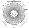
- Such an interconnect designated as an outer loop, has a starting region 144, a transition region 148, and an ending region 150.
- a plurality of the conductive traces are connected at their inner ends, at radius r 0 , by inner conductive loops 151, each inner conductive loop similarly having a starting region, a transition region, and an ending region.
- the combination of conductive traces 111, and their connecting structures provide for a winding structure on the surface(s) of the dielectric layer(s).
- the conductive traces 111 can be connected to conductive traces on other layers using interior layer connections such as vias or other interior layer links.
- interior layer connections such as vias or other interior layer links.
- the combination of the conductive traces on each of, for example, two (or more) layers combine to form an advantageous structure of multilayered windings as is well known in the field.
- a stator 100 may include multiple layers similar to the one illustrated in the planar view of Figure 1 .
- the multiple layers may be arranged to provide a sequence of coils or windings that are connected, usually in series, to form the poles of a motor or generator.
- the poles are then typically segregated into groups, with at least one group for each phase of current supplied to the motor (or generated by the generator).
- the arrangement of conductors for example, traces 111, and interconnecting conductive traces 151 and 153 in PCS 110) creates a rotating current density and associated magnetic field.
- This rotating current density can exert a torque on a surrounding magnetic structure (for a motor) or generate a current output (for a generator).
- the part of the printed circuit board with the radial structures 111 (the "active area") is the part of the stator designed to participate in this interaction.
- the active area of stator 100 may include conductive traces 111 coupled through interconnecting conductive traces 151 and 152 to form the rotating current.
- Some embodiments include two sets of rare-earth magnets fixed to a shaft passing through the center origin point 101 of PCS 110, which forms a compact, high-efficiency axial field synchronous electric device.
- stator 100 may include conductive elements in a peripheral area and conductive elements in an interior area. Conductive elements and can dissipate heat generated by stator 100, while in operation.
- a planar PCB for example, for a rotary electrical motor or generator, has inner, outer, and neutral end-turn structures which are shaped to optimize stator performance.
- end-turn design is of critical importance for the simple reason that end-turns serving different roles in the winding plan usually cannot co-exist on a single layer, and also cannot appear on a large number of layers as a method of reducing their total resistance.
- Another consideration for end-turns is that they are in close proximity to other conductive materials, for example, other structures on the same or adjacent layers, which can lead to eddy currents and parasitic loads at high frequencies.
- FEM finite element measurements
- end-turn in the following description should be understood to include similar features in inner and outer end turns, in links between pole groups, in cross-layer links, power connections, and in neutral tie-point structures. It is also important to recognize that while a major use of the technology disclosed herein is for no tears and generators, the application of the technology to any printed circuit board, single layer or multilayered, can be advantageous for reducing losses in the circuit. It is also important to note that within the motor/generator field, the number of end turns and their function will vary depending upon the number of phases, turns, and the poles for the motor.
- an inner or outer end turn has several connected regions.
- the basic functional part of an end-turn is a corner, a region that connects electrical current from an active region radial conductor or trace to a prescribed radius after the turn or corner is executed, typically changing the direction of the current on the planar surfaces from a substantially radially directed current to an angularly directed current.
- the turn connects to a narrow width radial trace at its beginning connection point, the width of the radially directed trace being dictated by the spacing of conductors in the active region of the plane and the space available for the angular part of the turn.
- the outer corner copper serves essentially no function in the conductivity of the structure, but by virtue of proximity to the high current density at the inner corner edge and other current sources on the PCS, may present an undesirable parasitic secondary to time-varying magnetic fields from such other sources. Further, the inner corner concentrates current and produces a magnetic field that may undesirably interact with other structures in the PCS. Collectively these effects lead to increased losses at higher frequencies, as well as a relatively higher resistance for the amount of copper used (because the copper at the outer edge of the corner carries substantially no current, as noted above).
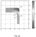
- the operation of the structure illustrated in Figure 6 is improved relative to the structure illustrated in Figure 5 (as shown by the FEM simulation of Figures 3A and 3B ), although the Figure 6 structure/shape still shows current concentration near the inner corner edge, and some copper at the outer corner edge still does not carry significant current.
- the conductivity of the structure illustrated in Figure 6 relative to Figure 5 is 1.046.
- the structure of Figure 6 therefore provides less resistance loss; however, the current density is still undesirably high at the inner corner edge resulting in the same undesirable effects noted in connection with the structure of Figure 5 , albeit at slightly lower levels.
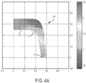
- An example embodiment described herein thus recognizes the need to obtain a further reduction from the high current densities of the earlier structures illustrated in Figures 2 and 5 , and Figures 3 and 6 , to determine a design shape and function which significantly reduces the concentration of current density along the inner corner, and specifically the inner corner edge, with the consequent reduction of the negative effects resulting from the high concentration of current density illustrated in Figures 2 and 3 .
- the end-turn structure illustrated there is bounded by its inner and outer edges, and corresponds to a local solution of a first-order differential equation in x and y (or r and ⁇ ).
- This example and preferred embodiment corresponding to a single-variable parameterization of a continuous transition from the starting width and location 710 of the end-turn corner 712, through the corner, to the x or theta directed portion 714 of the end turn.
- the smooth transition described in more detail below avoids the localized concentration of current in the corner transition found in the Figures 5 and 6 examples and does not tend to concentrate the current density in the turn. Accordingly the undesirable magnetic fields produced by earlier structures ( Figures 5 and 6 ) are minimized.
- the parameterization of the turn provides an independent variable that can be used for optimization purposes in different designs. As illustrated in Figure 4 , this end turn design avoids concentration of current density and magnetic field and has a relative conductivity of 1.197, almost 20% higher than the end-turn structure illustrated in Figure 5 .
- This equation provides for a gradual change of the radius of curvature along the edges and is controllable by a single parameter, ⁇ , selected depending upon the beginning and end points of the edge.
- the slope is a continuously changing variable having a zero second derivative.
- the avoidance of a concentration of current density in the loop can be viewed by measuring the current density along the inner edge of a loop in the starting region.
- the current density measurement will be higher in the beginning of the starting region where it connects to a conductive radial trace, and lowest at the inner edge at the intersection of the starting and transition regions.
- CT inner edge the inner edge section of the interconnect from the connection between the first conductive trace and the starting region to the beginning of the transition region.
- the current density achieves at least 90% of the maximum current density value, as determined by FEA/FEM calculations, within the first 20% of the CT inner edge measured along the inner edge of the interconnect from the first conductive trace toward the transition region. This differs substantially from the structures of Figures 5 and 6 wherein the peak occurs much further away from the radial conductor at a location which more likely adversely effects parasitic and eddy currents in nearby conductors.
- the distance of a conductor to a source of electromagnetic radiation can significantly affect the strength of the electromagnetic field impinging on the conductor and its adverse consequences.
- This "proximity" effect is the tendency for a current in an adjacent conductor to influence the distribution of current in a primary conductor, and vice versa. This effect results in a change of current distribution in the primary conductor as well as losses in both conductors, and is apparent as an increase in the electrical resistance of the primary conductor as the current frequency increases.
- a closely aligned concept is: the tendency of a conductive material that is not part of the circuit at DC to become a parasitic "secondary" due to a current density induced by a time varying current in the primary conductor.
- the parameter ⁇ determines the rate at which the end turn will approach its essentially constant radius, angularly directed, portion of the stator structure (the transition region).
- the corner needs to avoid interference with nearby structures. If the nearby structures are nested corners, such as those described by the corner equation and illustrated at 153 in Figure 1 , the outer edge of an inner end turn must be less than the "constant" radius of the inner edge of the adjacent outer end turn. Further, large values of ⁇ , may produce interference or minimum clearance violations with adjacent structures on the printed circuit board, such as termination structures that are not governed by the Corner Equation.
- ⁇ the angular displacement of two adjacent radial traces 111 such as those shown in Figure 1 .
- the angular separation ⁇ may be, for example, on the order of 3° (or 2 ⁇ /120 radians) or less.
- ⁇ is set to values that are too small, for example less than 0.1 ⁇ , effectively produces a square corner shape and reduces the advantages identified herein. Accordingly, a potential "range" for ⁇ where the angular separation between adjacent radial traces is, for example, between about 0.2 ⁇ and 0.06 ⁇ radians.
- the first radiused inner edge section and the second radiused inner edge section of the endloop in the starting and ending regions of the loop can each characterized by a slope dr/d ⁇ which is a linear function of r( ⁇ ) from a first conductive trace to the transitional region and where the slope is a different linear function from the transitional region to the conductive trace to be connected.
- the respective slope of the first radiused inner edge section and the second radiused inner edge section of the loop are each characterized by a monotonically changing value of slope as a function of the rotational angle from the one conductive trace to the conductive trace to be connected. This also reduces induced currents by reducing the aggregated current density at the corner.
- an example embodiment achieves at least 90% of the maximum current density value, as determined by FEA/FEM calculations, within the first 20% of the CT (as defined above) inner edge measured along the inner edge of an interconnect from the first conductive trace toward the transition region.
- Figure 8 shows a greatly expanded (in the z-axis) rendering of a motor stator stack up.
- the spacing between copper would be roughly the same as the copper thickness.
- conductive surfaces can be staggered in groups (groups of three as shown in Figure 8 are but one example configuration), in structure, and in function in order to maintain the necessary efficiencies of the overall device.
- all of the outer loops will not align for the full height of the stacked layers of the motor/generator stator, and advantages will be obtained in reduced electromagnetic fields generated at other than the active area of a board.
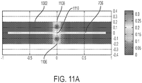
- an end turn loop 700 has an interconnecting trace which is split longitudinally into two or more parallel paths 704 for most of its length.
- the longitudinal split(s) have little effect on end-to-end conductivity, but does change the way in which time-varying flux is linked by the structure.
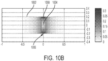
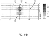
- the resulting current density induced in the end-turn segments separated by the slit(s) 706 (caused by narrow elongated region(s) of substantially no or zero electrical conductivity) is illustrated in Figures 10 and 11 by a simulation, using the same conditions, so that the effects can be compared across different embodiments, both in shape and magnitude. Further, the effect of the slits is to prevent a substantial increase in current density often seen when no slit or fewer slits are used.
- the FEM result displayed in Figure 10 shows a substantial effect of induced current caused by an external time-varying field at the origin 1004 of elongated trace 1002.
- the induced currents are particularly large at the origin, and the surface regions 1006 and 1008 vertically aligned with the origin.
- the longitudinal slit 706 in Figure 11 given a particular radial clearance for the end turn, necessarily reduces the cross-sectional area and therefore increases the DC resistance of the end-turn segment.
- the width of the slit is dependent on the copper thickness, which determines the minimum feature size achievable using the photoresist/etch process by which printed circuit boards are made.
- the number of slits in any given design is dependent on the flux leakage, other dB/dt sources, radial clearance for end turns, and the operating speed of the motor or generator design.
- the existence of these novel slits can substantially reduce induced current distributions in end turn, link, neutral, power connection, and similar features in a stator design, at both the origin and at the aligned surface regions. The physical extent of the effect of the induced current is also reduced.
- stator 100 A design consideration in stator 100 involves a trade-off between conduction and eddy current losses in the stator active area. To reduce conduction losses, the conductors must be wider (or connected in parallel on subsequent layers). To reduce eddy current losses, the effective areas capturing time-varying flux must be smaller, thus the conductors must be narrower.
- a third heat source involves eddy currents due to the magnetic field from current carrying conductors. This effect is important to consider in the inner and outer regions of the PCB, where different layers may perform different functions.
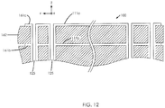
- FIG 12 illustrates a partial cross-sectional view of stator 100, according to some embodiments. Without limitation and for illustration purposes, a "z" axis is shown in the direction of the stacking of the different layers in stator 100, and a perpendicular axis 'r' is shown along its cross section. As seen, stator 100 may include a dielectric substrate 162 sandwiched between conductive layers 161a and 161b. Vias 125 provide electrical conductivity between conductive layers 161a and 161b.
- a via (or vias) 125 which is electrically conducting, may also provide thermal conductivity between layers 161a and 161b due to the conducting material that is typically used in these elements (e.g., copper, aluminum, tin, tungsten, and derived compounds).
- Dielectric substrate 162 may include any material used in PCBs, such as a composite material including woven fiberglass with an epoxy resin binder (e.g., FR-4 and the like). As illustrated in Figure 12 , the non-crosshatched regions, that is, the clear regions, are electrically conductive and vias 125 extend through the substrate providing electrical contact from the traces on one surface to the traces on the opposite surface of the substrate.
- stator 100 includes at least one of conductive elements 111, located on different conductive layers 161a and 161b.
- conductive element 111a may be one of the plurality of conductive elements 111 in the active area of stator 100 and disposed on conductive layer 161a.
- conductive element 111b may be one of the plurality of conductive elements 111 in the active area of stator 100 and disposed on a different conductive layer 161b.
- Figure 13 illustrates a detail of stator 100 including a plurality of conductive elements 111, disposed radially on PCS 110, according to some embodiments.
- Conductive elements 152, the inner loops are disposed angularly on PCS 110 and in this example embodiment, the outer loops are split along the slits 157.
- the inner loops illustrated here are not split due to the limited space available closer to the center of the stator.
- stator 100 further includes a plurality of third conductive elements extending radially from a radius greater than r 1 from center origin point 101 toward periphery 102 and disposed angularly on PCS 110, wherein at least one of the third conductive elements and at least one of the second conductive elements are coincident but located on different conductive layers.
- the third conductive elements may be included in conductive layer 161a, and the second conductive elements 121b may be included in conductive layer 161b.
- the radial conductive traces 111 can terminate at a termination connector 191 at a distance 142 ( r 1 ) from center origin point 101.
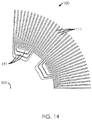
- Figure 14 illustrates a detail of an inner area proximal to center origin point 101 of stator 100, including a plurality of conducting elements 111 disposed radially and conductive elements 151 disposed angularly on PCS 110, according to some embodiments. Due to the spatial constraints near center origin point 101, in some embodiments only certain conductive elements 151 are electrically coupled to corresponding conductive elements 111. This arrangement avoids making undesirable electrical contact between adjacent conductive elements such as those used to enhance thermal energy dissipation, near center origin point 101.
- conductive elements such as end loops 151 can alternate or be staggered, with one end loop being on one layer of a multilayered PCS 110 and the other end loop being on an adjacent layer of PCS 110.
- staggering the end loops in different conductive layers, they can extend inward while maintaining a desired clearance between adjacent conductive elements on the same conductive layer.
- Other staggering configurations consistent with this feature may be envisioned, for example connecting every third or fourth conductive element through a via.
- the vias can extend not only between conductive layers on the surface of a single substrate, but across multiple layers as well.
- Some embodiments include one or more vias between layers near the outer portions of termination structure 115 to provide electrical connection between layers. These vias are typically employed in interlink connections, and in particular in connection with the outer and inner loops, to provide the winding structures required by the device. These connections can employ multiple vias, or only one via, extending through multiple layers to enable the connections necessary for the required circuit.
- the starting region of an inner or outer loop can be on a first layer, the ending region on a second layer, and the transition region can then include the interlink connections (for example, a trace wire connecting to the starting region, a via or other interlayer connector, and a second connecting trace connecting to the ending region).
- the traces of the starting region and the ending region will want to meet the terms of, for example, a Corner equation.
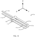
- connection configuration 615a includes conductive elements 111a,b and 121a,b in two different conductive layers (e.g., conductive layer 161a and 161b), forming an electrical coupling at termination structure 115. More specifically, connection configuration 615a provides electrical coupling between conductive elements 111a,b and conductive elements 121a,b.
- Figure 16 illustrates a flow chart for a method 800 for manufacturing a stator including a planar composite layer (PCS) having at least one dielectric layer and a plurality of conductive layers, according to some embodiments (for example, stator 100, PCS 110, dielectric substrate 162, conductive layers 161a, b).
- PCS planar composite layer
- Methods consistent with the present disclosure may include at least some, but not necessarily all, of the steps illustrated in method 800, and in some embodiments may be performed in a different sequence. Furthermore, methods consistent with the present disclosure may include at least two or more steps as in method 800 performed overlapping in time, or almost simultaneously.
- Step 802 includes forming a first conductive layer on the one surface of the PCS by radially disposing in accordance with the disclosure herein, first conductive elements on a dielectric substrate each starting from a first distance from a center origin point of the PCS and extending radially to a fixed outer radius.
- Step 804 includes forming a second conductive layer on a side of the substrate opposite the first conductive layer, by disposing a second conductive elements extending radially from a prefixed distance from the center origin point of the PCS.
- Step 806 includes forming a plurality of outer end loops in accordance with embodiments of the disclosure on both surfaces of the substrate, and coupling, in accordance with the disclosure herein, the first conductive elements to each other and to the second conductive elements through an interlink connection using the outer loops.
- Step 808 includes forming a plurality of inner end loops in accordance with embodiments of the disclosure on both surfaces of the substrate, and coupling, in accordance with the disclosure herein, the first conductive elements to each other and to the second conductive elements through an interlink connection using the inner loops.
- vias or other between surface connections can be employed.
- coupling the first conductive element with the second conductive elements may include a thermal coupling.
- the coupling can include a connection configuration having interlink structures including vias that go through the dielectric substrate from one conductive layer to another, non-adjacent, conductive layer (for example, using vias 125).
Landscapes
- Engineering & Computer Science (AREA)
- Power Engineering (AREA)
- Microelectronics & Electronic Packaging (AREA)
- Windings For Motors And Generators (AREA)
- Insulation, Fastening Of Motor, Generator Windings (AREA)
- Production Of Multi-Layered Print Wiring Board (AREA)
- Motor Or Generator Cooling System (AREA)
- Structure Of Printed Boards (AREA)
- Brushless Motors (AREA)
- Parts Printed On Printed Circuit Boards (AREA)
Description
- The present disclosure claims the benefit under 35 U.S.C. § 119(e) to
U.S. Provisional Pat. Appl. No. 62/236,407 62/236,422 U.S. Patent Application Serial Number 15/199,527 - Embodiments described herein are generally related to the field of reducing losses in printed circuit board devices. More specifically, embodiments as disclosed herein are related to the field of winding loss management in stators made on multi-layer printed circuit boards for electric motors and/or generators.
- The inventor has recognized and appreciated that current electric motors and other electric devices handling high currents through electrical leads in a printed circuit board (PCB) face multiple problems resulting from the electrical current flow in the PCB. Such problems include the generation of unwanted heat due to parasitic or eddy currents, which can lead to mechanical failure and destructive mechanical interferences with the rotor of the motor or generator, as well as other inefficiencies in the operation of the motor or generator. As a byproduct of the increased current density flow in regions of the electrical circuit, high temperature gradients in the PCB caused by, inter alia, high electrical current gradients may lead to structural damage of the PCB, such as delamination, or localized failure or degradation of the electrical leads or the dielectric material in the substrate. More importantly, perhaps, these high electric current densities act to generate undesirable larger electromagnetic fields which can create, for example, parasitic and eddy currents in physically nearby regions of the electric circuits, which in turn can act as a drag on the motor or generator rotor and thereby reduce its power output and efficiency.
- Printed circuit board electric devices built without the advantageous features described hereinafter, employ a variety of strategies to make connections between electrical current carrying traces laid down on the PCB surface, or surfaces in the case of a multilayer board device, of the dielectric substrates found in these devices. These strategies, however, do not address, or recognize in any substantial way, the disadvantages resulting from enhanced current density in portions of the electric circuit traces and the adverse results therefrom.
-
WO 2004/073365 A2 concerns an axial rotary energy device which is arranged in a multi-phase electric current configuration. The device includes a rotor having a plurality of permanent magnet poles secured thereto and further includes a stator formed by stacking a plurality of printed circuit board working conductor layers together with a plurality of printed circuit board connecting layers. The stator having at least one working conductor layer for each phase of the electric current and at least one connecting conductor layer associated with one working conducting layer. The working conductor layer and the connecting conductor layer each having radial conductors extending from an inner diameter through-hole to an outer diameter through-hole. A plurality of via conductors are provided for electrically connecting selected ones of the radial connectors of the connecting conductor layer to selected ones of the radial connectors of the working conductor layers through the through-holes. - A particular example embodiment of the disclosure relates to printed circuit board motors and generators. Windings formed from copper in printed circuit boards have been used for purposes of forming antennas, inductors, transformers, and stators that can be incorporated in permanent magnet brushless DC (permanent magnet synchronous) machines. For energy conversion devices using modern permanent magnet materials and PCB stators, the magnetic field is not strongly confined by magnetically susceptible materials. Thus, the interaction between fields from adjacent turns in a winding, and/or windings on adjacent layers (for a multilayer configuration) may be significant. The structures disclosed hereinafter reduce the effective resistance in the windings, and therefore reduce the associated losses to achieve a specified current density in rotating energy conversion devices. The effect of the disclosed structures is a measurable reduction in loss mechanisms as a function of increasing frequency, compared to the currently available devices. These effects are significant in frequency ranges important to energy conversion processes as well as typical control strategies, for example, pulse-width modulation.
- Disclosed is the structure of an electrical motor or generator stator which includes a planar composite structure (PCS) having at least one dielectric layer and a plurality of conductive layers. The PCS is characterized at least in part by a center origin point and a periphery. The stator can also include a plurality of first elements, radially extending conductive traces, which extend from an inner radial distance rs to an outer radial distance r 1, the radii being measured from the center origin point toward the periphery of the PCS. The traces are generally angularly disposed on the PCS. The plurality of first radially extending elements are each connected at their inner and outer ends to enable winding loops, and other circuit structures, to be formed. When the elements are connected in such loops, the outer ends of the elements are connected using outer loop interconnects and the inner ends of the elements are connected using inner loop interconnects as described in more detail hereinafter. Further, according to some example embodiments of the disclosure, at least one of the first radial conductive elements is connected to at least one other of the radial conductive elements at their respective outer radius ends. Also, first conductive elements are connected at their inner radius ends to other radially conductive elements. There can result plural closed loops having multiple windings and forming the stator, for example, of an electrical motor or generator.
- Also disclosed is an electrical motor or generator having a stator which includes a PCS with at least one dielectric layer and at least one conductive layer, the PCS being characterized at least in part by a center origin point and a periphery. The stator can also include a plurality of first electrically conductive traces extending radially from a starting radius, r 0, from the center origin point toward the periphery of the PCS and disposed angularly on the PCS. A plurality of the conductive traces connect through a respective associated interconnect to at least one other conductive trace extending radially from an inner radius r 0 from the center origin point radially outward toward the periphery of the PCS and disposed angularly from the associated conductive trace.
- In an example embodiment, a stator is provided according to
claim 1. - Also disclosed is a stator having a planar composite structure (PCS) having at least one dielectric layer and a conductive pattern on a surface of each said dielectric layer. At least one conductive pattern has a plurality of first conductive traces, each extending radially from an inner radius to an outer radius and disposed angularly on one of the dielectric surfaces. At least one of the first conductive traces connected at its outer radius to at least one other of the first conductive elements at its outer radius by a first interconnect, and wherein at least the first interconnect is bounded by inner and outer edges, and has a starting region, a transition region, and an ending region, and the starting region has a first radiused inner edge section and a first radiused outer edge section extending from the first conductive trace to the transition region, and a second radiused inner edge section and a second radiused outer edge section extending from the transition region to the other conductive trace. At least the first radiused inner and outer edge sections and the second radiused inner and outer edge sections are each characterized at least in part by the Corner Equation

s -θ)/α for a corner evaluated with θ < θs and ending at θs and rs. - Also disclosed is a stator having a planar composite structure (PCS) with at least one dielectric layer and a conductive pattern on a surface of each said dielectric layer. At least one conductive pattern has a plurality of first conductive traces, each extending radially from an inner radius to an outer radius and disposed angularly on one of the dielectric surfaces. At least one of the first conductive traces is connected at its outer radius to at least one other of the first conductive elements at its outer radius by a first interconnect. The first interconnect is bounded by an inner edge and an outer edge. The first interconnect has a starting region, a transition region, and an ending region, and the inner edge of the starting region has a first radiused inner edge section extending from the first conductive trace at its outer radius to the transition region, and a second radiused inner edge section extending from the transition region to the other conductive trace at its outer radius. At least the first radiused inner edge section and the second radiused inner edge section are each characterized by a slope dr/dθ which is a linear function of r(θ) from the one conductive trace to the transitional region and where the slope is a different linear function from the transitional region to the other conductive trace.
- Also disclosed is a stator having a planar composite structure (PCS) comprising at least one dielectric layer and a conductive pattern on a surface of each said dielectric layer. At least one conductive pattern has a plurality of first conductive traces, each extending radially from an inner radius to an outer radius and disposed angularly on one of the dielectric surfaces. At least one of the first conductive traces is connected at its outer radius to a starting region of a first interconnect. The first interconnect is bounded by inner and outer edges, and the first interconnect having the starting region, a transition region, and an ending region, and a first radiused inner edge section extending from the outer radius of the one conductive trace to the transition region, and a second radiused inner edge section extending from the transition region to the other conductive trace at its outer radius. At any point between the inner and outer edge, the smallest current density magnitude under direct current excitation is not less than 50% of the largest current density magnitude evaluated along the shortest line between the inner and outer edge passing through that point.
- Also disclosed is a stator, having a planar composite structure (PCS) having at least two dielectric layers and a conductive pattern on a surface of each said dielectric layer. At least one conductive pattern has a plurality of first conductive traces, each extending radially from an inner radius to an outer radius and disposed angularly on different ones of the dielectric surfaces. At least one of the first conductive traces is connected at its outer radius to at least one other of the first conductive traces on a different surface at its outer radius by a first interlayer interconnect. The interconnect is substantially bounded by inner and outer edges. The first interlayer interconnect has a starting region on a first layer, a transition region, and an ending region on a different layer, and further has a first radiused inner edge section extending from a first conductive trace to the transition region, and a second radiused inner edge section extending from the transition region to the other conductive trace at its outer radius; and wherein at least the first radiused inner edge section and the second radiused inner edge section are each characterized at least in part by a structure designed to reduce parasitic and eddy current effects on axially adjacent conductive surface structures.
- Also disclosed is a stator having a planar composite structure (PCS) having at least one dielectric layer and a conductive pattern on a surface of each the dielectric layer. At least one conductive pattern has a plurality of first conductive traces, each extending radially from an inner radius to an outer radius and disposed angularly on one of the dielectric surfaces. At least one of the first conductive traces is connected at its outer radius to at least one other of the first conductive elements at its outer radius by a first interconnect first interconnect is bounded by inner and outer edges. The first interconnect has a starting region, a transition region, an ending region, and a first radiused inner edge section extending from the connected first conductive trace at its outer radius to the transition region, and a second radiused inner edge section connecting the transition region to the outer radius of the one other conductive trace. At least the first radiused inner edge section and the second radiused inner edge section are each characterized by a structure for reducing eddy currents in the outer conductive portions of the interconnect.
- Also disclosed is a stator having a planar composite structure (PCS) with at least one dielectric layer and a conductive pattern on a surface of each said dielectric layer. The at least one conductive pattern has a plurality of first conductive traces, each extending radially from an inner radius to an outer radius and disposed angularly on one of the dielectric surfaces; with at least one of the first conductive traces connected at its outer radius to at least one other of the first conductive traces at its outer radius by a first interconnect, the first interconnect bounded by inner and outer edges. The first interconnect has a starting region, a transition region, and an ending region, and first radiused inner and outer edge sections extending from the first conductive trace to its transition region, and second radiused inner and outer edge sections extending from the transition region to the one other conductive trace at its outer radius. At least the respective slope of the first radiused inner edge section and the second radiused inner edge section are each characterized by a monotonically changing value of slope as a function of the rotational angle from the one conductive trace to the other conductive trace.
- Also disclosed is a stator having a planar composite structure (PCS) with at least one dielectric layer and a conductive pattern on a surface of each said dielectric layer. At least one conductive pattern has a plurality of first conductive traces, each extending radially from an inner radius to an outer radius and disposed angularly on one of the dielectric surfaces, at least one of the first conductive traces being connected at its outer radius to at least one other of the first conductive traces at its outer radius by a first interconnect. The first interconnect is bounded by inner and outer edges. The first interconnect has a starting region, a transition region, an ending region, and a first radiused inner edge section and a first radiused outer edge section extending from the first conductive trace to the transition region, and a second radiused inner edge section and a second radiused outer edge section extending from the transition region to the one other conductive trace at the outer radius of the other conductive trace. At least between an inner edge section and an outer edge section of the interconnect in its transition region, the interconnect has at least one slit-like elongated region that does not substantially reduce electrical conductivity from one end of the interconnect to the other end of the interconnect, the slit-like elongated region extending substantially parallel to the inner edge section in the transition region of the interconnect.
- Also disclosed is a stator having a planar composite structure (PCS) having at least one dielectric layer and a conductive pattern on a surface of each said dielectric layer. At least one conductive pattern has a plurality of first conductive traces, each extending radially from an inner radius to an outer radius and disposed angularly on one of the dielectric surfaces. At least one of the first conductive traces is connected at its outer radius to at least one other of the first conductive traces at its outer radius by a first interconnect. The first interconnect is bounded at least by inner and outer edges. The first interconnect has a starting region, a transition region, and an ending region, and a first radiused inner edge section extending from the first conductive trace to the transition region, and a second radiused inner edge section extending from the transition region to the one other conductive trace at the outer radius of the other conductive trace. The inner edge of the interconnect from the connection between the first conductive trace and the starting region to the beginning of the transition region is designated the "CT inner edge" distance. An example embodiment achieves at least 90% of the maximum current density value, as determined by FEA/FEM calculations, within the first 20% of the CT inner edge measured along the inner edge of the interconnect from the first conductive trace toward the transition region.
-
-
Figure 1 illustrates a plan view of a stator including a PCS having at least one dielectric layer with one of a plurality of conductive layers being illustrated in accordance with some embodiments of the disclosure; -
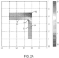
Figure 2A is a black-and-white copy of a color illustration of an FEM solution for current density in an end-turn corner with sharp corners; -
Figure 2B is a grayscale version of the FEM solution shown inFig. 2A ; -
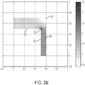
Figure 3A is a black-and-white copy of a color illustration of an FEM solution for current density in an end-turn corner structure with radius corners wherein the radius corresponds to the half-width of the smaller trace; -
Figure 3B is a grayscale version of the FEM solution shown inFig. 3A ; -
Figure 4A is a black-and-white copy of a color illustration of an FEM solution for current density in accordance with an example embodiment of the disclosure; -
Figure 4B is a grayscale version of the FEM solution shown inFig. 4A ; -
Figure 5 illustrates a plan view of a stator including a PCS in accordance with a prior art structure having sharp corners; -
Figure 6 illustrates a plan view of a stator including a PCS wherein the corners have a constant turning radius; -
Figure 7 illustrates details of an outer loop connection in a stator, each connection configuration including a first starting region connecting to a transition region connecting in turn to a termination region, according to some embodiments of the disclosure; -
Figure 8 illustrates a greatly expanded, in the z axis, motor stator stack up; -
Figure 9 illustrates an end turn loop having an interconnecting trace which is split longitudinally; -
Figure 10A is a black-and-white copy of a color illustration of an FEM solution showing a resulting current density without the narrow elongated slit-like regions illustrated inFigure 9 ; -
Figure 10B is a grayscale version of the FEM solution shown inFig. 10A ; -
Figure 11A is a black-and-white copy of a color illustration of an FEM solution showing a resulting current density with the narrow elongated slit-like regions illustrated inFigure 9 ; -
Figure 11B is a grayscale version of the FEM solution shown inFig. 11A ; -
Figure 12 illustrates a cross-sectional view of a section ofstator 100 according to some embodiments; -
Figure 13 illustrates a detail ofstator 100 including a plurality ofconductive elements 111 disposed on the PCS; -
Figure 14 illustrates a detail of an inner area of the stator proximal to the center origin point; -
Figure 15 illustrates a perspective view of connection configurations according to some embodiments of the disclosure; and -
Figure 16 is a flow chart in a method for manufacturing a stator including a planar composite layer (PCS) having at least one dielectric layer and a plurality of conductive layers, according to some embodiments. - In the figures, elements and steps denoted by the same reference numerals are associated with the same or similar elements and steps, unless indicated otherwise.
- Referring to
Figure 1 , in an example embodiment of the disclosure, a plan view of astator 100 for use in an electrically driven motor or a rotating generator, has a planar composite structure (PCS) 110 with at least one dielectric layer and a plurality of substrate layers havingconductive traces 111 thereon. The diameter of the stator shown inFigure 1 can be on the order of cm to tens of meters. Conductive traces 111 can be part of a winding structure in accordance with an embodiment of the disclosure that can be connected at the outer annulus and inner section of a PCB structure.PCS 110 is characterized at least in part by acenter origin point 101 and anouter periphery 102.Stator 100 includes a plurality of firstconductive traces 111 extending radially from a radius 140 (r0) (measured from the center origin point 101) to a radius 142 (r 1) (measured from center origin point 101) towardperiphery 102 ofPCS 110 and disposed angularly on the PCS. One or more of the first conductive traces are connected at their outer end, at radius r1, to typically one or more other of the first conductive trace(s) at its outer radius r1. Such an interconnect, designated as an outer loop, has astarting region 144, atransition region 148, and an endingregion 150. - In a complementary manner, a plurality of the conductive traces are connected at their inner ends, at radius r0, by inner
conductive loops 151, each inner conductive loop similarly having a starting region, a transition region, and an ending region. In this manner, the combination ofconductive traces 111, and their connecting structures, provide for a winding structure on the surface(s) of the dielectric layer(s). - In more complex structures, the
conductive traces 111 can be connected to conductive traces on other layers using interior layer connections such as vias or other interior layer links. In these interlayer connections, the combination of the conductive traces on each of, for example, two (or more) layers combine to form an advantageous structure of multilayered windings as is well known in the field. - There is a concern, however, that the current passing from one
conductive trace 111 to the next conductive trace does not create electromagnetic fields which may damage or reduce the efficiency of the operating system of the motor or generator. Such negative effects can result, for example, in parasitic currents or eddy currents in nearby electrically conductive structures which can act as a drag on the system. As is explained further below, such drag reduces efficiency, and is not typically considered in the structural design of the motor or generator ofFigure 1 . However the present disclosure is directed to reducing substantially, by proper shaping and design of the interconnectingend loops - Thus, a
stator 100 may include multiple layers similar to the one illustrated in the planar view ofFigure 1 . The multiple layers may be arranged to provide a sequence of coils or windings that are connected, usually in series, to form the poles of a motor or generator. The poles are then typically segregated into groups, with at least one group for each phase of current supplied to the motor (or generated by the generator). Collectively, when properly controlled by an external electric circuit, the arrangement of conductors (for example, traces 111, and interconnecting conductive traces 151 and 153 in PCS 110) creates a rotating current density and associated magnetic field. This rotating current density (and magnetic field) can exert a torque on a surrounding magnetic structure (for a motor) or generate a current output (for a generator). The part of the printed circuit board with the radial structures 111 (the "active area") is the part of the stator designed to participate in this interaction. Accordingly, the active area ofstator 100 may includeconductive traces 111 coupled through interconnecting conductive traces 151 and 152 to form the rotating current. Some embodiments include two sets of rare-earth magnets fixed to a shaft passing through thecenter origin point 101 ofPCS 110, which forms a compact, high-efficiency axial field synchronous electric device. In addition to the active area including a rotating current density that interacts with an inhomogeneous magnetic field,stator 100 may include conductive elements in a peripheral area and conductive elements in an interior area. Conductive elements and can dissipate heat generated bystator 100, while in operation. - In accordance with the structure of the disclosure, a planar PCB, for example, for a rotary electrical motor or generator, has inner, outer, and neutral end-turn structures which are shaped to optimize stator performance. In a planar PCB motor stator, or planar composite stator (PCS), the end turn design is of critical importance for the simple reason that end-turns serving different roles in the winding plan usually cannot co-exist on a single layer, and also cannot appear on a large number of layers as a method of reducing their total resistance. Another consideration for end-turns is that they are in close proximity to other conductive materials, for example, other structures on the same or adjacent layers, which can lead to eddy currents and parasitic loads at
high frequencies. - The present disclosure addresses both issues, and can be compared to other design strategies and structures through use of finite element measurements (FEM). The use of "end-turn" in the following description should be understood to include similar features in inner and outer end turns, in links between pole groups, in cross-layer links, power connections, and in neutral tie-point structures. It is also important to recognize that while a major use of the technology disclosed herein is for no tears and generators, the application of the technology to any printed circuit board, single layer or multilayered, can be advantageous for reducing losses in the circuit. It is also important to note that within the motor/generator field, the number of end turns and their function will vary depending upon the number of phases, turns, and the poles for the motor.
- As noted above, an inner or outer end turn has several connected regions. The basic functional part of an end-turn is a corner, a region that connects electrical current from an active region radial conductor or trace to a prescribed radius after the turn or corner is executed, typically changing the direction of the current on the planar surfaces from a substantially radially directed current to an angularly directed current. Often, the turn connects to a narrow width radial trace at its beginning connection point, the width of the radially directed trace being dictated by the spacing of conductors in the active region of the plane and the space available for the angular part of the turn. For purposes of illustration, and because the feature under consideration is approximately (locally) Cartesian, the angular travel in the embodiments that follow is indicated on the x-axis, while the radial travel is indicated on the y-axis. There is a conformal map between this case and the cylindrical coordinate case directly applicable to the PCS for axial field machines.
- To explore the relationship between structure or shape of the end turn design, and its performance, FEM simulations of several example designed structures and examples from earlier designs are described with the condition that each structure carry exactly the same total current. Plots of current density magnitude within a structure were subsequently produced from the FEM solution, and are illustrated in
Figures 2-4 . The scales in these plots are adjusted so that they can be compared. It should be appreciated that in the black-and-white versions of the color drawings presented herein (i.e.,Figures 2A ,3A ,4A ,10A and11A ), the darker regions do not necessarily correspond to higher current density regions in the FEM solutions and the lighter regions do not necessarily correspond to lower current density regions in those solutions. This is true because the red and blue regions near the top and bottom, respectively, of the scales for the colored versions both copied as a darker color in the black-and-white versions. Accordingly, it is helpful to consider the grayscale versions of the FEM solutions (i.e.,Figures 2B ,3B ,4B ,10B and11B ) in conjunction with the black-and-white copies of the colored versions of those solutions to better understand the relative current densities in the various regions. - It is common for prior printed circuit board CAD packages to merge lines of different widths with square corners, as illustrated in
Figure 5 . End turns with corners drawn this way appear, for example, in United States patent7,109,625 . An adverse consequence of this structure, as shown in the FEM produced current density map inFigures 2A and2B , is that the current is concentrated significantly at theinner corner 250 of theinner edge section 251 of the end turn. This creates a concentration of current, and hence energy loss at the inner edge corner, and the current is essentially zero at theouter corner edge 252. The concentration of current at the inner edge corner leads to a much stronger magnetic field H (amperes per meter, or A/m) in the immediate vicinity of the inner edge corner. The outer corner copper serves essentially no function in the conductivity of the structure, but by virtue of proximity to the high current density at the inner corner edge and other current sources on the PCS, may present an undesirable parasitic secondary to time-varying magnetic fields from such other sources. Further, the inner corner concentrates current and produces a magnetic field that may undesirably interact with other structures in the PCS. Collectively these effects lead to increased losses at higher frequencies, as well as a relatively higher resistance for the amount of copper used (because the copper at the outer edge of the corner carries substantially no current, as noted above). - The actual end-to-end conductivity of the structure in
Figure 5 varies in a predictable fashion as a function of material conductivity, thickness, and scale. For purposes of comparison and to emphasize the importance of end-turn corner shape independent of these other variables, the conductivity of the structure inFigure 5 is designated as 1.000. - It is important to note, for the
Figure 5 shape/structure, that while the current entering thestarting region 254 of the end turn is substantially uniform across the entire cross-sectional extent of the trace, in making the sharp turn it tends to congregate inward. - Another common practice in CAD tools is to provide the option of merging lines with the application of a specified constant turning radius at the turn. Often the radii at the inner
radiused corner 642 and outerradiused corner 645 used to replace the sharp corner ofFigure 5 are chosen based on the widths of the lines to be merged. The geometry of the corner illustrated inFigure 6 shows this type of end turn corner. Note that inFigure 6 , there are 3 nestedend loops 635. In this case, the inner and outer radii forinner edge 640 andouter edge 650 are the same as the radius of the aperture used for the vertical trace segment. The operation of the structure illustrated inFigure 6 is improved relative to the structure illustrated inFigure 5 (as shown by the FEM simulation ofFigures 3A and3B ), although theFigure 6 structure/shape still shows current concentration near the inner corner edge, and some copper at the outer corner edge still does not carry significant current. The conductivity of the structure illustrated inFigure 6 relative toFigure 5 is 1.046. The structure ofFigure 6 therefore provides less resistance loss; however, the current density is still undesirably high at the inner corner edge resulting in the same undesirable effects noted in connection with the structure ofFigure 5 , albeit at slightly lower levels. - An example embodiment described herein thus recognizes the need to obtain a further reduction from the high current densities of the earlier structures illustrated in
Figures 2 and5 , andFigures 3 and6 , to determine a design shape and function which significantly reduces the concentration of current density along the inner corner, and specifically the inner corner edge, with the consequent reduction of the negative effects resulting from the high concentration of current density illustrated inFigures 2 and3 . - Referring to
Figure 7 , the end-turn structure illustrated there is bounded by its inner and outer edges, and corresponds to a local solution of a first-order differential equation in x and y (or r and θ). This example and preferred embodiment, corresponding to a single-variable parameterization of a continuous transition from the starting width andlocation 710 of the end-turn corner 712, through the corner, to the x or theta directedportion 714 of the end turn. The smooth transition described in more detail below avoids the localized concentration of current in the corner transition found in theFigures 5 and6 examples and does not tend to concentrate the current density in the turn. Accordingly the undesirable magnetic fields produced by earlier structures (Figures 5 and6 ) are minimized. The parameterization of the turn provides an independent variable that can be used for optimization purposes in different designs. As illustrated inFigure 4 , this end turn design avoids concentration of current density and magnetic field and has a relative conductivity of 1.197, almost 20% higher than the end-turn structure illustrated inFigure 5 . Further, in one particular example embodiment of the disclosure, the inner and outer edges can be shaped in accordance with the so-called "Corner equation":
s -θ)/α for a corner evaluated with θ < θs and ending at θs and rs. This equation provides for a gradual change of the radius of curvature along the edges and is controllable by a single parameter, α, selected depending upon the beginning and end points of the edge. In a preferred embodiment, the slope is a continuously changing variable having a zero second derivative. This is equivalent to saying that the radiused edge is characterized by a slope, which is a linear function of r from the starting point, (the intersection between the starting region and the conductive trace) to the transition region and that the slope is a different linear function from the transitional region to the end of the ending region. - The avoidance of a concentration of current density in the loop (inner or outer) can be viewed by measuring the current density along the inner edge of a loop in the starting region. Typically, the current density measurement will be higher in the beginning of the starting region where it connects to a conductive radial trace, and lowest at the inner edge at the intersection of the starting and transition regions. If the inner edge section of the interconnect from the connection between the first conductive trace and the starting region to the beginning of the transition region is designated the "CT inner edge" distance, then in an example embodiment, the current density achieves at least 90% of the maximum current density value, as determined by FEA/FEM calculations, within the first 20% of the CT inner edge measured along the inner edge of the interconnect from the first conductive trace toward the transition region. This differs substantially from the structures of
Figures 5 and6 wherein the peak occurs much further away from the radial conductor at a location which more likely adversely effects parasitic and eddy currents in nearby conductors. - As noted above, the distance of a conductor to a source of electromagnetic radiation can significantly affect the strength of the electromagnetic field impinging on the conductor and its adverse consequences. This "proximity" effect is the tendency for a current in an adjacent conductor to influence the distribution of current in a primary conductor, and vice versa. This effect results in a change of current distribution in the primary conductor as well as losses in both conductors, and is apparent as an increase in the electrical resistance of the primary conductor as the current frequency increases. A closely aligned concept is: the tendency of a conductive material that is not part of the circuit at DC to become a parasitic "secondary" due to a current density induced by a time varying current in the primary conductor. This effect increases as (i) the frequency goes up, (ii) the strength of the magnetic field increases, and (iii) as the proximity of the parasitic conducting material to the primary decreases. These considerations mitigate in favor of both reducing the concentration of the electromagnetic field, for example, by using the example corner shape structure illustrated in
Figure 7 , and reducing the proximity of the conductor where possible to adjacent conductors. In a preferred example embodiment of the disclosure, the "corner equation" specified hereinafter helps ameliorate both of these effects. - For either of the equations above, the parameter α determines the rate at which the end turn will approach its essentially constant radius, angularly directed, portion of the stator structure (the transition region). An important consideration is that the corner needs to avoid interference with nearby structures. If the nearby structures are nested corners, such as those described by the corner equation and illustrated at 153 in
Figure 1 , the outer edge of an inner end turn must be less than the "constant" radius of the inner edge of the adjacent outer end turn. Further, large values of α, may produce interference or minimum clearance violations with adjacent structures on the printed circuit board, such as termination structures that are not governed by the Corner Equation. With these considerations in mind, the determination of a suitable value of α can be inferred from the angular displacement (designated as δ) of two adjacent radial traces 111 such as those shown inFigure 1 . In a typical stator, having for example, 120 radial traces, the angular separation δ may be, for example, on the order of 3° (or 2π/120 radians) or less. Further, while a minimum fabrication clearance will factor into a precise calculation of the largest possible α for a given design, it is undesirable to use an α that is too large since the width of the complete end turn structure may be reduced, with the effect of increasing DC resistance of the structure. On the other hand, setting α to values that are too small, for example less than 0.1δ, effectively produces a square corner shape and reduces the advantages identified herein. Accordingly, a potential "range" for α where the angular separation between adjacent radial traces is, for example, between about 0.2δ and 0.06δ radians. - In addition to the Corner equation described above, there are other descriptions of forming and shaping the corner of an end loop or trace which also ameliorate the effects seen when the corner is "sharp." Thus, for example, as described above, and in the context of an end loop as described above in connection with, for example, and
loop 714 illustrated inFigure 7 , the first radiused inner edge section and the second radiused inner edge section of the endloop in the starting and ending regions of the loop can each characterized by a slope dr/dθ which is a linear function of r(θ) from a first conductive trace to the transitional region and where the slope is a different linear function from the transitional region to the conductive trace to be connected. - In another description of the forming and shaping of the corner of in the end loop, one can select any point between the inner and outer edge of the loop, and shape the loop, so that the smallest current density magnitude under direct current excitation at that point is not less than 50% of the largest current density magnitude evaluated along the shortest line between the inner and outer edge of the loop and passing through that point. This approach accordingly also reduces the adverse effects of aggregated current density.
- In yet another description for forming and shaping the corner of an end loop, the respective slope of the first radiused inner edge section and the second radiused inner edge section of the loop are each characterized by a monotonically changing value of slope as a function of the rotational angle from the one conductive trace to the conductive trace to be connected. This also reduces induced currents by reducing the aggregated current density at the corner. In yet another approach to reducing aggregated current density, an example embodiment achieves at least 90% of the maximum current density value, as determined by FEA/FEM calculations, within the first 20% of the CT (as defined above) inner edge measured along the inner edge of an interconnect from the first conductive trace toward the transition region.
- In practical stator designs, out-of-plane structures may also form parasitic secondary elements.
Figure 8 shows a greatly expanded (in the z-axis) rendering of a motor stator stack up. In actual construction, the spacing between copper would be roughly the same as the copper thickness. This illustrates the considerable complexity of the notion of "proximity", which can vary based on stator design parameters such as pole count, number of turns, etc. Accordingly, as shown in the Figure, conductive surfaces can be staggered in groups (groups of three as shown inFigure 8 are but one example configuration), in structure, and in function in order to maintain the necessary efficiencies of the overall device. Thus, for example, all of the outer loops will not align for the full height of the stacked layers of the motor/generator stator, and advantages will be obtained in reduced electromagnetic fields generated at other than the active area of a board. - Referring to
Figure 9 , anend turn loop 700 has an interconnecting trace which is split longitudinally into two or moreparallel paths 704 for most of its length. The longitudinal split(s) have little effect on end-to-end conductivity, but does change the way in which time-varying flux is linked by the structure. The resulting current density induced in the end-turn segments separated by the slit(s) 706 (caused by narrow elongated region(s) of substantially no or zero electrical conductivity) is illustrated inFigures 10 and11 by a simulation, using the same conditions, so that the effects can be compared across different embodiments, both in shape and magnitude. Further, the effect of the slits is to prevent a substantial increase in current density often seen when no slit or fewer slits are used. - The FEM result displayed in
Figure 10 shows a substantial effect of induced current caused by an external time-varying field at theorigin 1004 ofelongated trace 1002. The induced currents are particularly large at the origin, and thesurface regions longitudinal slit 706 inFigure 11 , given a particular radial clearance for the end turn, necessarily reduces the cross-sectional area and therefore increases the DC resistance of the end-turn segment. Further, the width of the slit is dependent on the copper thickness, which determines the minimum feature size achievable using the photoresist/etch process by which printed circuit boards are made. Thus, the number of slits in any given design is dependent on the flux leakage, other dB/dt sources, radial clearance for end turns, and the operating speed of the motor or generator design. Advantageously, however, as illustrated inFigure 11 , the existence of these novel slits can substantially reduce induced current distributions in end turn, link, neutral, power connection, and similar features in a stator design, at both the origin and at the aligned surface regions. The physical extent of the effect of the induced current is also reduced. - A design consideration in
stator 100 involves a trade-off between conduction and eddy current losses in the stator active area. To reduce conduction losses, the conductors must be
wider (or connected in parallel on subsequent layers). To reduce eddy current losses, the effective areas capturing time-varying flux must be smaller, thus the conductors must be narrower. - A third heat source involves eddy currents due to the magnetic field from current carrying conductors. This effect is important to consider in the inner and outer regions of the PCB, where different layers may perform different functions.
-
Figure 12 illustrates a partial cross-sectional view ofstator 100, according to some embodiments. Without limitation and for illustration purposes, a "z" axis is shown in the direction of the stacking of the different layers instator 100, and a perpendicular axis 'r' is shown along its cross section. As seen,stator 100 may include adielectric substrate 162 sandwiched betweenconductive layers Vias 125 provide electrical conductivity betweenconductive layers layers Dielectric substrate 162 may include any material used in PCBs, such as a composite material including woven fiberglass with an epoxy resin binder (e.g., FR-4 and the like). As illustrated inFigure 12 , the non-crosshatched regions, that is, the clear regions, are electrically conductive and vias 125 extend through the substrate providing electrical contact from the traces on one surface to the traces on the opposite surface of the substrate. - Accordingly, in some embodiments,
stator 100 includes at least one ofconductive elements 111, located on differentconductive layers conductive element 111a may be one of the plurality ofconductive elements 111 in the active area ofstator 100 and disposed onconductive layer 161a. Correspondingly, conductive element 111b may be one of the plurality ofconductive elements 111 in the active area ofstator 100 and disposed on a differentconductive layer 161b. -
Figure 13 illustrates a detail ofstator 100 including a plurality ofconductive elements 111, disposed radially onPCS 110, according to some embodiments.Conductive elements 152, the inner loops, are disposed angularly onPCS 110 and in this example embodiment, the outer loops are split along theslits 157. The inner loops illustrated here are not split due to the limited space available closer to the center of the stator. In some embodiments,stator 100 further includes a plurality of third conductive elements extending radially from a radius greater than r1 fromcenter origin point 101 towardperiphery 102 and disposed angularly onPCS 110, wherein at least one of the third conductive elements and at least one of the second conductive elements are coincident but located on different conductive layers. For example, and without loss of generality, the third conductive elements may be included inconductive layer 161a, and the secondconductive elements 121b may be included inconductive layer 161b. - In the illustrated embodiment of
Figure 13 , the radialconductive traces 111 can terminate at atermination connector 191 at a distance 142 (r 1) fromcenter origin point 101. These connectors are described in more detail in co-pendingUS application serial number 15/199,527 identified and incorporated by reference above. -
Figure 14 illustrates a detail of an inner area proximal tocenter origin point 101 ofstator 100, including a plurality of conductingelements 111 disposed radially andconductive elements 151 disposed angularly onPCS 110, according to some embodiments. Due to the spatial constraints nearcenter origin point 101, in some embodiments only certainconductive elements 151 are electrically coupled to correspondingconductive elements 111. This arrangement avoids making undesirable electrical contact between adjacent conductive elements such as those used to enhance thermal energy dissipation, nearcenter origin point 101. In addition, to address the issue of thermal and electrical conductivity in the highly constrained space of the inner area ofPCS 110, conductive elements such asend loops 151 can alternate or be staggered, with one end loop being on one layer of amultilayered PCS 110 and the other end loop being on an adjacent layer ofPCS 110. By staggering the end loops, in different conductive layers, they can extend inward while maintaining a desired clearance between adjacent conductive elements on the same conductive layer. Other staggering configurations consistent with this feature may be envisioned, for example connecting every third or fourth conductive element through a via. The vias can extend not only between conductive layers on the surface of a single substrate, but across multiple layers as well. - Some embodiments include one or more vias between layers near the outer portions of
termination structure 115 to provide electrical connection between layers. These vias are typically employed in interlink connections, and in particular in connection with the outer and inner loops, to provide the winding structures required by the device. These connections can employ multiple vias, or only one via, extending through multiple layers to enable the connections necessary for the required circuit. Thus, the starting region of an inner or outer loop can be on a first layer, the ending region on a second layer, and the transition region can then include the interlink connections (for example, a trace wire connecting to the starting region, a via or other interlayer connector, and a second connecting trace connecting to the ending region). In this configuration, as in the configurations shown for example inFigure 7 , the traces of the starting region and the ending region will want to meet the terms of, for example, a Corner equation. -
Figure 15 shows a perspective view ofconnection configuration 615a, according to some embodiments.Connection configuration 615a includesconductive elements 111a,b and 121a,b in two different conductive layers (e.g.,conductive layer termination structure 115. More specifically,connection configuration 615a provides electrical coupling betweenconductive elements 111a,b andconductive elements 121a,b. -
Figure 16 illustrates a flow chart for amethod 800 for manufacturing a stator including a planar composite layer (PCS) having at least one dielectric layer and a plurality of conductive layers, according to some embodiments (for example,stator 100,PCS 110,dielectric substrate 162,conductive layers 161a, b). - Methods consistent with the present disclosure may include at least some, but not necessarily all, of the steps illustrated in
method 800, and in some embodiments may be performed in a different sequence. Furthermore, methods consistent with the present disclosure may include at least two or more steps as inmethod 800 performed overlapping in time, or almost simultaneously. - Step 802 includes forming a first conductive layer on the one surface of the PCS by radially disposing in accordance with the disclosure herein, first conductive elements on a dielectric substrate each starting from a first distance from a center origin point of the PCS and extending radially to a fixed outer radius. Step 804 includes forming a second conductive layer on a side of the substrate opposite the first conductive layer, by disposing a second conductive elements extending radially from a prefixed distance from the center origin point of the PCS.
- Step 806 includes forming a plurality of outer end loops in accordance with embodiments of the disclosure on both surfaces of the substrate, and coupling, in accordance with the disclosure herein, the first conductive elements to each other and to the second conductive elements through an interlink connection using the outer loops. Step 808 includes forming a plurality of inner end loops in accordance with embodiments of the disclosure on both surfaces of the substrate, and coupling, in accordance with the disclosure herein, the first conductive elements to each other and to the second conductive elements through an interlink connection using the inner loops. In
step 810, vias or other between surface connections can be employed. - In some embodiments, coupling the first conductive element with the second conductive elements may include a thermal coupling. Furthermore, the coupling can include a connection configuration having interlink structures including vias that go through the dielectric substrate from one conductive layer to another, non-adjacent, conductive layer (for example, using vias 125).
- One skilled in the art will realize the disclosure may be embodied in other specific forms without departing from the spirit or essential characteristics thereof. The foregoing embodiments are therefore to be considered in all respects illustrative rather than limiting of the disclosure described herein. The scope of the disclosure is thus indicated by the appended claims, rather than by the foregoing description.
- Various aspects of the present invention may be used alone, in combination, or in a variety of arrangements not specifically discussed in the embodiments described in the foregoing and is therefore not limited in this application to the details and arrangement of components set forth in the foregoing description or illustrated in the drawings. For example, aspects described in one embodiment may be combined in any manner with aspects described in other embodiments.
- Use of ordinal terms such as "first," "second," "third," etc. in the claims to modify a claim element does not by itself connote any priority, precedence or order of one claim element over another or the temporal order in which acts of a method are performed, but are used merely as labels to distinguish one claimed element having a certain name from another element having a same name (but for use of the ordinal term) to distinguish the claim elements.
- Also, the phraseology and terminology used herein is used for the purpose of description and should not be regarded as limiting. The use of "including," "comprising," or "having," "containing," "involving," and variations thereof herein, is meant to encompass the items listed thereafter and equivalents thereof as well as additional items.
Claims (9)
- A stator, comprising:a planar composite structure, PCS (110), comprising at least one dielectric layer and a conductive pattern on a surface of each said dielectric layer, the conductive pattern comprising;a plurality of conductive traces (111), each extending radially from an inner radius measured from a center origin point (101) to an outer radius measured from the center origin point (101) and disposed angularly on the dielectric surface; andat least a first one of the conductive traces (111) connected at its outer radius to a second one of the conductive traces (111) at its outer radius by a first interconnect (153),wherein the first interconnect (153) is bounded by an inner edge and an outer edge, and has a starting region (710), a transition region (714) and an ending region, the starting region (710) having a first radiused inner edge section extending from the first one of the conductive traces (111) to the transition region (714), and the ending region having a second radiused inner edge section extending from the transition region to the second one of the conductive traces (111);characterized in thatthe first radiused inner edge section and the second radiused inner edge section are each characterized at least in part by the Corner Equation

 that the first radiused inner edge section and the second radiused inner edge section each have a radius of curvature which gradually changes along its edge.
 - The stator of any one of claim 1, wherein:the starting region (710) has a first radiused outer edge section extending from the first one of the conductive traces (111) to the transition region (714), and a second radiused outer edge section extending from the transition region (714) to the second one of the conductive traces (111);the first radiused outer edge section and the second radiused outer edge section are each characterized at least in part by the Corner Equation

 the first radiused outer edge section has a radius of curvature which gradually changes along its edge; andthe second radiused outer edge section has a radius of curvature which gradually changes along its edge.
 - The stator of claim 1 or claim 2, wherein the stator is a multi-layer stator, and further including a connecting structure for interconnecting the starting region of one conductive trace (111) to the ending region of another conductive trace (111) on a different layer.
- The stator of any one of claims 1 to 3, wherein the stator is included in an axial flux motor or generator that includes a rotor operatively associated with the stator.
- The stator of any of one of claims 1 to 4, wherein the angular separation between two adjacent conductive traces (111) is δ radians, and
α ranges between 0.06δ and 0.2δ radians. - The stator of any one of claims 1 to 5, wherein at least the first radiused inner edge section and the second radiused inner edge section are each characterized by a slope dr/dθ which is a linear function of r(θ) from the first one of the conductive traces (111) to the transition region (714) and where the slope dr/dθ is a different linear function from the transition region (714) to the second one of the conductive traces (111).
- The stator of any one of claims 1 to 6, wherein a slope of the first radiused inner edge section is characterized by a continuously changing value of slope as a function of a rotational angle from the first one of the conductive traces (111) to the second one of the conductive traces (111).
- The stator of any one of claims 1 to 7, wherein a slope of the first radiused inner edge section is characterized by a monotonically changing value of slope as a function of a rotational angle from the first one of the conductive traces (111) to the second one of the conductive traces (111).
- The stator of any one of claims 1 to 8, wherein at least between the inner edge and the outer edge of the first interconnect (153) in its transition region (714), the first interconnect has at least one slit-like elongated region that does not substantially reduce electrical conductivity from one end of the first interconnect (153) to the other end of the first interconnect (153), and extending substantially parallel to the inner edge in the transition region (714) of the first interconnect (153).
Priority Applications (1)
| Application Number | Priority Date | Filing Date | Title |
|---|---|---|---|
| PL16778659T PL3357144T3 (en) | 2015-10-02 | 2016-09-30 | Printed circuit board stator |
Applications Claiming Priority (4)
| Application Number | Priority Date | Filing Date | Title |
|---|---|---|---|
| US201562236422P | 2015-10-02 | 2015-10-02 | |
| US201562236407P | 2015-10-02 | 2015-10-02 | |
| US15/199,527 US9673684B2 (en) | 2015-10-02 | 2016-06-30 | Structures and methods for thermal management in printed circuit board stators |
| PCT/US2016/054794 WO2017059257A1 (en) | 2015-10-02 | 2016-09-30 | Structures and methods for controlling losses in printed circuit boards |
Publications (2)
| Publication Number | Publication Date |
|---|---|
| EP3357144A1 EP3357144A1 (en) | 2018-08-08 |
| EP3357144B1 true EP3357144B1 (en) | 2021-02-17 |
Family
ID=57113815
Family Applications (3)
| Application Number | Title | Priority Date | Filing Date |
|---|---|---|---|
| EP16784315.0A Active EP3357147B1 (en) | 2015-10-02 | 2016-09-30 | Structures and methods for thermal management in printed circuit board stators |
| EP16778659.9A Active EP3357144B1 (en) | 2015-10-02 | 2016-09-30 | Printed circuit board stator |
| EP19184929.8A Withdrawn EP3570412A1 (en) | 2015-10-02 | 2016-09-30 | Structures and methods for thermal management in printed circuit board stators |
Family Applications Before (1)
| Application Number | Title | Priority Date | Filing Date |
|---|---|---|---|
| EP16784315.0A Active EP3357147B1 (en) | 2015-10-02 | 2016-09-30 | Structures and methods for thermal management in printed circuit board stators |
Family Applications After (1)
| Application Number | Title | Priority Date | Filing Date |
|---|---|---|---|
| EP19184929.8A Withdrawn EP3570412A1 (en) | 2015-10-02 | 2016-09-30 | Structures and methods for thermal management in printed circuit board stators |
Country Status (19)
| Country | Link |
|---|---|
| US (1) | US9673684B2 (en) |
| EP (3) | EP3357147B1 (en) |
| JP (2) | JP6892855B2 (en) |
| KR (2) | KR102354538B1 (en) |
| CN (2) | CN108141089B (en) |
| AU (2) | AU2016331798B2 (en) |
| BR (2) | BR112018006116B1 (en) |
| CA (2) | CA3000002C (en) |
| DK (2) | DK3357144T3 (en) |
| ES (2) | ES2857909T3 (en) |
| HK (2) | HK1251361A1 (en) |
| MX (3) | MX2018003948A (en) |
| MY (1) | MY189408A (en) |
| PH (2) | PH12018500722A1 (en) |
| PL (2) | PL3357144T3 (en) |
| RU (2) | RU2719305C1 (en) |
| TW (2) | TWI705658B (en) |
| WO (2) | WO2017059257A1 (en) |
| ZA (2) | ZA201801922B (en) |
Families Citing this family (24)
| Publication number | Priority date | Publication date | Assignee | Title |
|---|---|---|---|---|
| US11121614B2 (en) | 2017-06-05 | 2021-09-14 | E-Circuit Motors, Inc. | Pre-warped rotors for control of magnet-stator gap in axial flux machines |
| US9800109B2 (en) * | 2015-10-02 | 2017-10-24 | E-Circuit Motors, Inc. | Structures and methods for controlling losses in printed circuit boards |
| US9859763B2 (en) * | 2015-10-02 | 2018-01-02 | E-Circuit Motors, Inc. | Structures and methods for controlling losses in printed circuit boards |
| US11527933B2 (en) | 2015-10-02 | 2022-12-13 | E-Circuit Motors, Inc. | Stator and rotor design for periodic torque requirements |
| US10170953B2 (en) | 2015-10-02 | 2019-01-01 | E-Circuit Motors, Inc. | Planar composite structures and assemblies for axial flux motors and generators |
| US11342813B2 (en) * | 2016-04-30 | 2022-05-24 | Blue Canyon Technologies Inc. | Printed circuit board axial flux motor with thermal element |
| US10186922B2 (en) | 2017-01-11 | 2019-01-22 | Infinitum Electric Inc. | System and apparatus for axial field rotary energy device |
| US11177726B2 (en) | 2017-01-11 | 2021-11-16 | Infinitum Electric, Inc. | System and apparatus for axial field rotary energy device |
| US10340760B2 (en) | 2017-01-11 | 2019-07-02 | Infinitum Electric Inc. | System and apparatus for segmented axial field rotary energy device |
| US11831211B2 (en) | 2017-06-05 | 2023-11-28 | E-Circuit Motors, Inc. | Stator and rotor design for periodic torque requirements |
| US11005322B2 (en) | 2017-06-05 | 2021-05-11 | E-Circuit Motors, Inc. | Rotor assemblies for axial flux machines |
| TWI786130B (en) * | 2017-07-10 | 2022-12-11 | 美商E電路馬達股份有限公司 | Improved planar composite structures for axial flux motors and generators |
| WO2019190959A1 (en) | 2018-03-26 | 2019-10-03 | Infinitum Electric Inc. | System and apparatus for axial field rotary energy device |
| CN112997383B (en) | 2018-11-01 | 2024-05-31 | 电路电机有限公司 | Stator and rotor design for periodic torque demand |
| US20200212741A1 (en) | 2018-12-26 | 2020-07-02 | Blue Canyon Technologies Inc. | Axial flux motor |
| US11283319B2 (en) | 2019-11-11 | 2022-03-22 | Infinitum Electric, Inc. | Axial field rotary energy device with PCB stator having interleaved PCBS |
| AU2020382759A1 (en) | 2019-11-12 | 2022-05-26 | E-Circuit Motors, Inc. | Improved rotor assemblies for axial flux machines |
| US20210218304A1 (en) | 2020-01-14 | 2021-07-15 | Infinitum Electric, Inc. | Axial field rotary energy device having pcb stator and variable frequency drive |
| CN111416488B (en) * | 2020-04-01 | 2021-01-05 | 江苏苏杭电子有限公司 | Processing method of red copper coil for special motor |
| EP3961880A1 (en) * | 2020-08-31 | 2022-03-02 | Siemens Aktiengesellschaft | Active part of an electric machine with printed conductor |
| WO2022177855A1 (en) | 2021-02-17 | 2022-08-25 | E-Circuit Motors, Inc. | Planar stator configurations for axial flux machines |
| US11482908B1 (en) | 2021-04-12 | 2022-10-25 | Infinitum Electric, Inc. | System, method and apparatus for direct liquid-cooled axial flux electric machine with PCB stator |
| CN118056343A (en) | 2021-07-30 | 2024-05-17 | 电路电机有限公司 | Magnetic material filled printed circuit board and printed circuit board stator |
| US11336130B1 (en) * | 2021-08-17 | 2022-05-17 | E-Circuit Motors, Inc. | Low-loss planar winding configurations for an axial flux machine |
Family Cites Families (89)
| Publication number | Priority date | Publication date | Assignee | Title |
|---|---|---|---|---|
| US2970238A (en) | 1959-02-12 | 1961-01-31 | Printed Motors Inc | Printed circuit armature |
| CH376570A (en) * | 1959-11-13 | 1964-04-15 | S E A Societe D Electronique E | Rotating electric machine with axial air gap |
| US3096455A (en) | 1962-03-08 | 1963-07-02 | Basic Motor Developments Inc | Printed disc electrical machinery |
| NL7802552A (en) * | 1967-04-03 | 1978-06-30 | Kollmorgen Corp | Aluminium armature method |
| DE2409681A1 (en) * | 1974-02-28 | 1975-09-11 | Retobobina Handelsanstalt | ELECTRIC ANCHOR WRAP |
| US4115915A (en) | 1975-07-31 | 1978-09-26 | General Electric Company | Process for manufacturing motor having windings constructed for automated assembly |
| JPS5836145A (en) | 1981-08-28 | 1983-03-03 | Kangiyou Denki Kiki Kk | Laminated wiring unit |
| JPS59213287A (en) | 1983-05-18 | 1984-12-03 | Kokusai Dengiyou Kk | Attracting device with rotor by dc electromagnet |
| DE3526166C2 (en) * | 1984-07-23 | 1996-05-02 | Asahi Chemical Ind | Brushless electric motor and method of manufacturing a coil unit therefor |
| CH660542A5 (en) | 1984-08-31 | 1987-04-30 | Asgalium Sa | ELECTRIC MOTOR. |
| JPH0669005B2 (en) * | 1986-02-13 | 1994-08-31 | ソニー株式会社 | Multi-layer sheet coil |
| US4733115A (en) | 1986-12-16 | 1988-03-22 | Eastman Kodak Company | Electric motor |
| US5099162A (en) | 1987-07-22 | 1992-03-24 | Canon Kabushiki Kaisha | Coil of superconducting material for electric appliance and motor utilizing said coil |
| US5332460A (en) | 1988-08-09 | 1994-07-26 | Nippon Seiko Kabushiki Kaisha | Method of manufacturing a seal ring for magnetic fluid seal device |
| KR910010797A (en) | 1989-11-29 | 1991-06-29 | 서주인 | Coil Pattern of Frequency Generator |
| DE4125044A1 (en) * | 1991-07-29 | 1993-02-04 | Wolfgang Hill | ELECTRIC MOTOR DESIGNED AS A DISC RUNNER WITH RADIAL AND RADIAL PACKAGE ARRANGED TO THE ROTATIONAL AXIS |
| EP0563852A1 (en) | 1992-04-02 | 1993-10-06 | Siemens Aktiengesellschaft | Zag fuse for reduced blow-current applications |
| KR940011416B1 (en) * | 1992-11-24 | 1994-12-15 | 포항종합제철주식회사 | Control method of tapping |
| WO1995034935A1 (en) | 1994-06-15 | 1995-12-21 | Philips Electronics N.V. | Flat electric motor |
| US5710476A (en) | 1995-01-31 | 1998-01-20 | Interscience, Inc. | Armature design for an axial-gap rotary electric machine |
| DE19503511C5 (en) | 1995-02-03 | 2010-11-04 | Siemens Ag | Synchronous linear motor |
| JP3508957B2 (en) * | 1995-05-17 | 2004-03-22 | 株式会社安川電機 | Sheet coil type resolver |
| JPH10322156A (en) * | 1996-06-10 | 1998-12-04 | Fuji Electric Co Ltd | Noise filter for power inverter |
| US6411002B1 (en) * | 1996-12-11 | 2002-06-25 | Smith Technology Development | Axial field electric machine |
| US5982069A (en) * | 1998-06-30 | 1999-11-09 | Rao; Dantam K. | Axial gap machine phase coil having tapered conductors with increasing width in radial direction |
| DE69930643T2 (en) | 1999-01-14 | 2006-08-17 | Kabushiki Kaisha Yaskawa Denki, Kitakyushu | PULSE TRANSDUCER WITH SINGLE SPOOL |
| US7112910B2 (en) | 2001-06-26 | 2006-09-26 | Rotys Inc. | Brushless DC electric motor |
| WO2004073365A2 (en) * | 2003-02-07 | 2004-08-26 | Core Innovation, Llc | Conductor optimized axial field rotary energy device |
| JP2004270544A (en) | 2003-03-07 | 2004-09-30 | Matsushita Electric Ind Co Ltd | Magnetization jig, electric compressor, assembling method of rotor, and assembling method of electric compressor |
| US7582999B2 (en) * | 2003-11-20 | 2009-09-01 | Intelligent Electric Motor Solutions Pty Ltd | Electric machine having a magnetically inducible core |
| DE102004021661A1 (en) * | 2004-05-03 | 2005-12-15 | BSH Bosch und Siemens Hausgeräte GmbH | Commutator motor with several field winding groups |
| CH697889B1 (en) | 2004-05-07 | 2009-03-13 | Etel Sa | Method and device for positioning and fixing the magnet on a magnetic yoke of a motor. |
| US20060055265A1 (en) | 2004-09-16 | 2006-03-16 | Zalusky James T | Printed circuit board motor |
| US8058762B2 (en) | 2005-01-19 | 2011-11-15 | Daikin Industries, Ltd. | Rotor, axial gap type motor, method of driving motor, and compressor |
| DE202005021283U1 (en) | 2005-03-09 | 2007-10-04 | Fiedler, Joachim | Magnetic holder |
| JP2007059507A (en) | 2005-08-23 | 2007-03-08 | Keihin Corp | Substrate mounting transformer |
| EP1826889B1 (en) | 2006-02-24 | 2015-09-30 | ThyssenKrupp Aufzugswerke GmbH | Method and apparatus for mounting magnets |
| US7750522B2 (en) | 2006-07-18 | 2010-07-06 | Danotek Motion Technologies | Slow-speed direct-drive generator |
| US9129741B2 (en) | 2006-09-14 | 2015-09-08 | Qualcomm Incorporated | Method and apparatus for wireless power transmission |
| JP2008099429A (en) * | 2006-10-11 | 2008-04-24 | Asmo Co Ltd | Print coil and print motor |
| US20080100166A1 (en) | 2006-10-26 | 2008-05-01 | Deere & Company | Motor having stator with generally planar windings |
| US8558425B2 (en) | 2006-10-26 | 2013-10-15 | Deere & Company | Motor having stator with generally planar windings |
| WO2008134796A1 (en) | 2007-05-03 | 2008-11-13 | In Motion Technologies Pty Ltd | Rotor magnet positioning device |
| TW200913438A (en) | 2007-09-13 | 2009-03-16 | Metal Ind Res & Dev Ct | Slot-less windings applied to rotating electronic devices and the manufacturing method thereof |
| WO2009068079A1 (en) | 2007-11-27 | 2009-06-04 | Ina Drives & Mechatronics Gmbh & Co. Ohg | Electronically commutated disc rotor motor with a large number of composite printed circuit boards which comprise conductor layers |
| FR2927736B1 (en) * | 2008-02-20 | 2014-12-05 | Leroy Somer Moteurs | STATOR OF ROTATING ELECTRIC MACHINE. |
| US7800471B2 (en) | 2008-04-04 | 2010-09-21 | Cedar Ridge Research, Llc | Field emission system and method |
| US8368495B2 (en) | 2008-04-04 | 2013-02-05 | Correlated Magnetics Research LLC | System and method for defining magnetic structures |
| US20100000112A1 (en) | 2008-07-02 | 2010-01-07 | Whirlpool Corporation | Dispensing dryer dosing sensing |
| US9257876B2 (en) | 2008-11-14 | 2016-02-09 | Metal Industries Research & Development Centre | Motor integrated to electronic device |
| TWI425742B (en) | 2008-11-14 | 2014-02-01 | Metal Ind Res & Dev Ct | Integrated in the electronic device of the motor |
| US8823241B2 (en) | 2009-01-16 | 2014-09-02 | Boulder Wind Power, Inc. | Segmented stator for an axial field device |
| MY183588A (en) | 2009-03-30 | 2021-02-27 | Tianjin Tasly Pharmaceutical Co Ltd | New salvianolic acid compound l, preparation method and use thereof |
| US8450404B2 (en) | 2009-06-16 | 2013-05-28 | Honeywell Federal Manufacturing & Technologies, Llc | Compositions containing borane or carborane cage compounds and related applications |
| US9279852B2 (en) | 2009-11-30 | 2016-03-08 | Essai, Inc. | Systems and methods for conforming test tooling to integrated circuit device profiles with sockets having secured and replaceable bushings |
| CN102341996B (en) * | 2009-12-22 | 2013-09-04 | 株式会社Cosmomechanics | Disc-type coil |
| US8225497B2 (en) | 2010-01-05 | 2012-07-24 | General Electric Company | Permanent magnet rotor installation systems |
| US9154024B2 (en) | 2010-06-02 | 2015-10-06 | Boulder Wind Power, Inc. | Systems and methods for improved direct drive generators |
| JP5545110B2 (en) | 2010-08-06 | 2014-07-09 | ブラザー工業株式会社 | Control device and computer program for printing |
| GB2485185A (en) | 2010-11-04 | 2012-05-09 | Pipera Technologies Ltd | Axial gap electrical machine having integrated stator |
| JP5644551B2 (en) * | 2011-01-31 | 2014-12-24 | 日立工機株式会社 | Disc motor and electric working machine |
| WO2012142230A2 (en) | 2011-04-12 | 2012-10-18 | Smith James S | Air gap control systems and methods |
| EP2697895B1 (en) | 2011-04-13 | 2019-09-04 | Boulder Wind Power, Inc. | Flux focusing arrangement for permanent magnets, methods of fabricating such arrangements, and machines including such arrangements |
| US9011514B2 (en) | 2011-08-22 | 2015-04-21 | Cook Medical Technologies Llc | Emergency vessel repair prosthesis deployment system |
| US20130052491A1 (en) | 2011-08-26 | 2013-02-28 | Roger Neil Bull | Thermal management system for a multi-cell array |
| TWI440281B (en) | 2011-08-31 | 2014-06-01 | Sunonwealth Electr Mach Ind Co | Motor stator |
| JP5880817B2 (en) * | 2011-09-28 | 2016-03-09 | 日立工機株式会社 | Disk motor and electric working machine equipped with the same |
| DE102011086214A1 (en) | 2011-11-11 | 2013-05-16 | Magnet-Physik Dr. Steingroever Gmbh | Method and device for holding magnet bodies during their magnetization and for introducing the magnetized magnet bodies into a component of a magnetic system |
| WO2013122543A1 (en) | 2012-02-13 | 2013-08-22 | Agency For Science, Technology And Research | Motor and method for assembling the same |
| KR101882700B1 (en) | 2012-07-18 | 2018-07-30 | 삼성디스플레이 주식회사 | Chip on glass substrate and method for measureing connection resistance of the same |
| TWI487883B (en) | 2012-07-19 | 2015-06-11 | Ind Tech Res Inst | Readout apparatus and driving method for sensor |
| US8339019B1 (en) | 2012-07-30 | 2012-12-25 | Boulder Wind Power, Inc. | Structure for an electromagnetic machine having compression and tension members |
| US8716913B2 (en) | 2012-08-07 | 2014-05-06 | Boulder Wind Power, Inc. | Devices and methods for magnetic pole and back iron retention in electromagnetic machines |
| CN103001426A (en) | 2012-11-19 | 2013-03-27 | 腾达电动科技镇江有限公司 | Printed circuit board disk type motor without iron core |
| US20140152136A1 (en) | 2012-12-03 | 2014-06-05 | Boulder Wind Power, Inc. | Devices and methods for magnetic pole retention in electromagnetic machines |
| US20140201291A1 (en) | 2013-01-16 | 2014-07-17 | Long Russell | System and Method for Creating a Geographically-Defined Social Network |
| US8723052B1 (en) | 2013-02-27 | 2014-05-13 | Boulder Wind Power, Inc. | Methods and apparatus for optimizing electrical interconnects on laminated composite assemblies |
| US8785784B1 (en) | 2013-03-13 | 2014-07-22 | Boulder Wind Power, Inc. | Methods and apparatus for optimizing structural layout of multi-circuit laminated composite assembly |
| US8736133B1 (en) | 2013-03-14 | 2014-05-27 | Boulder Wind Power, Inc. | Methods and apparatus for overlapping windings |
| US20140262499A1 (en) | 2013-03-14 | 2014-09-18 | Boulder Wind Power, Inc. | Methods and apparatus for optimizing electrically inoperative zones on laminated composite assemblies |
| US8941961B2 (en) | 2013-03-14 | 2015-01-27 | Boulder Wind Power, Inc. | Methods and apparatus for protection in a multi-phase machine |
| CN104426263B (en) | 2013-08-26 | 2017-12-19 | 苏州奥宝杰电机科技有限公司 | Rotor and the brushless electric machine using the rotor |
| US20150084446A1 (en) | 2013-09-24 | 2015-03-26 | Electro-Motor Dynamics, LLC | Direct drive stacked motor acuator |
| JP2015115973A (en) * | 2013-12-09 | 2015-06-22 | 株式会社安川電機 | Rotor of rotary electric machine and rotary electric machine |
| US9793775B2 (en) | 2013-12-31 | 2017-10-17 | Boulder Wind Power, Inc. | Methods and apparatus for reducing machine winding circulating current losses |
| US20150188391A1 (en) | 2013-12-31 | 2015-07-02 | Boulder Wind Power, Inc. | Apparatus for cooling an electromagnetic machine |
| WO2015134855A1 (en) | 2014-03-07 | 2015-09-11 | Boulder Wind Power, Inc. | Methods and apparatus for integrated machine segmentation |
| US9899886B2 (en) | 2014-04-29 | 2018-02-20 | Boulder Wind Power, Inc. | Devices and methods for magnetic flux return optimization in electromagnetic machines |
| US10177620B2 (en) | 2014-05-05 | 2019-01-08 | Boulder Wind Power, Inc. | Methods and apparatus for segmenting a machine |
-
2016
- 2016-06-30 US US15/199,527 patent/US9673684B2/en active Active
- 2016-09-30 WO PCT/US2016/054794 patent/WO2017059257A1/en active Application Filing
- 2016-09-30 BR BR112018006116-6A patent/BR112018006116B1/en active IP Right Grant
- 2016-09-30 CN CN201680057552.3A patent/CN108141089B/en active Active
- 2016-09-30 EP EP16784315.0A patent/EP3357147B1/en active Active
- 2016-09-30 AU AU2016331798A patent/AU2016331798B2/en active Active
- 2016-09-30 JP JP2018517347A patent/JP6892855B2/en active Active
- 2016-09-30 PL PL16778659T patent/PL3357144T3/en unknown
- 2016-09-30 DK DK16778659.9T patent/DK3357144T3/en active
- 2016-09-30 EP EP16778659.9A patent/EP3357144B1/en active Active
- 2016-09-30 WO PCT/US2016/054704 patent/WO2017059213A1/en active Application Filing
- 2016-09-30 KR KR1020187012461A patent/KR102354538B1/en active IP Right Grant
- 2016-09-30 ES ES16778659T patent/ES2857909T3/en active Active
- 2016-09-30 PL PL16784315T patent/PL3357147T3/en unknown
- 2016-09-30 BR BR112018006113-1A patent/BR112018006113B1/en active IP Right Grant
- 2016-09-30 JP JP2018517269A patent/JP7008623B2/en active Active
- 2016-09-30 AU AU2016329080A patent/AU2016329080B2/en active Active
- 2016-09-30 RU RU2018115808A patent/RU2719305C1/en active
- 2016-09-30 DK DK16784315.0T patent/DK3357147T3/en active
- 2016-09-30 MX MX2018003948A patent/MX2018003948A/en unknown
- 2016-09-30 ES ES16784315T patent/ES2792028T3/en active Active
- 2016-09-30 CA CA3000002A patent/CA3000002C/en active Active
- 2016-09-30 MX MX2018003949A patent/MX2018003949A/en unknown
- 2016-09-30 RU RU2018115809A patent/RU2719307C1/en active
- 2016-09-30 EP EP19184929.8A patent/EP3570412A1/en not_active Withdrawn
- 2016-09-30 MY MYPI2018701291A patent/MY189408A/en unknown
- 2016-09-30 KR KR1020187012460A patent/KR102412683B1/en active IP Right Grant
- 2016-09-30 CN CN201680057559.5A patent/CN108141111B/en active Active
- 2016-09-30 TW TW105131805A patent/TWI705658B/en active
- 2016-09-30 CA CA2999999A patent/CA2999999C/en active Active
- 2016-10-03 TW TW105131938A patent/TWI722024B/en active
-
2018
- 2018-03-22 ZA ZA2018/01922A patent/ZA201801922B/en unknown
- 2018-03-22 ZA ZA201801923A patent/ZA201801923B/en unknown
- 2018-03-28 MX MX2021006740A patent/MX2021006740A/en unknown
- 2018-04-02 PH PH12018500722A patent/PH12018500722A1/en unknown
- 2018-04-02 PH PH12018500723A patent/PH12018500723A1/en unknown
- 2018-08-17 HK HK18110622.5A patent/HK1251361A1/en unknown
- 2018-08-17 HK HK18110621.6A patent/HK1251360A1/en unknown
Non-Patent Citations (1)
| Title |
|---|
| None * |
Also Published As
Similar Documents
| Publication | Publication Date | Title |
|---|---|---|
| US10256690B2 (en) | Structures and methods for controlling losses in printed circuit boards | |
| EP3357144B1 (en) | Printed circuit board stator | |
| US9800109B2 (en) | Structures and methods for controlling losses in printed circuit boards | |
| US9859763B2 (en) | Structures and methods for controlling losses in printed circuit boards | |
| US10355550B2 (en) | Methods and apparatus for reducing machine winding circulating current losses | |
| US8736133B1 (en) | Methods and apparatus for overlapping windings | |
| CN105071573B (en) | A kind of stator structure with printed circuit board (PCB) winding | |
| US8723052B1 (en) | Methods and apparatus for optimizing electrical interconnects on laminated composite assemblies | |
| US8785784B1 (en) | Methods and apparatus for optimizing structural layout of multi-circuit laminated composite assembly | |
| US8471669B2 (en) | Disc-type coil | |
| US9018822B2 (en) | Stator for rotary electric machine | |
| US20200091805A1 (en) | Dynamo-electric machine with reduced cogging torque | |
| CA3066776A1 (en) | Improved planar composite structures and assemblies for axial flux motors and generators | |
| JP6327158B2 (en) | Power conversion circuit | |
| CN216873054U (en) | Linear motor | |
| KR20150134763A (en) | stator assembly for a rotating electric device |
Legal Events
| Date | Code | Title | Description |
|---|---|---|---|
| STAA | Information on the status of an ep patent application or granted ep patent |
Free format text: STATUS: THE INTERNATIONAL PUBLICATION HAS BEEN MADE |
|
| PUAI | Public reference made under article 153(3) epc to a published international application that has entered the european phase |
Free format text: ORIGINAL CODE: 0009012 |
|
| STAA | Information on the status of an ep patent application or granted ep patent |
Free format text: STATUS: REQUEST FOR EXAMINATION WAS MADE |
|
| 17P | Request for examination filed |
Effective date: 20180321 |
|
| AK | Designated contracting states |
Kind code of ref document: A1 Designated state(s): AL AT BE BG CH CY CZ DE DK EE ES FI FR GB GR HR HU IE IS IT LI LT LU LV MC MK MT NL NO PL PT RO RS SE SI SK SM TR |
|
| AX | Request for extension of the european patent |
Extension state: BA ME |
|
| DAV | Request for validation of the european patent (deleted) | ||
| DAX | Request for extension of the european patent (deleted) | ||
| REG | Reference to a national code |
Ref country code: HK Ref legal event code: DE Ref document number: 1251360 Country of ref document: HK |
|
| STAA | Information on the status of an ep patent application or granted ep patent |
Free format text: STATUS: EXAMINATION IS IN PROGRESS |
|
| 17Q | First examination report despatched |
Effective date: 20190516 |
|
| GRAP | Despatch of communication of intention to grant a patent |
Free format text: ORIGINAL CODE: EPIDOSNIGR1 |
|
| STAA | Information on the status of an ep patent application or granted ep patent |
Free format text: STATUS: GRANT OF PATENT IS INTENDED |
|
| INTG | Intention to grant announced |
Effective date: 20201126 |
|
| GRAS | Grant fee paid |
Free format text: ORIGINAL CODE: EPIDOSNIGR3 |
|
| GRAA | (expected) grant |
Free format text: ORIGINAL CODE: 0009210 |
|
| STAA | Information on the status of an ep patent application or granted ep patent |
Free format text: STATUS: THE PATENT HAS BEEN GRANTED |
|
| AK | Designated contracting states |
Kind code of ref document: B1 Designated state(s): AL AT BE BG CH CY CZ DE DK EE ES FI FR GB GR HR HU IE IS IT LI LT LU LV MC MK MT NL NO PL PT RO RS SE SI SK SM TR |
|
| REG | Reference to a national code |
Ref country code: GB Ref legal event code: FG4D |
|
| REG | Reference to a national code |
Ref country code: CH Ref legal event code: NV Representative=s name: HGF GMBH, CH Ref country code: CH Ref legal event code: EP |
|
| REG | Reference to a national code |
Ref country code: DE Ref legal event code: R096 Ref document number: 602016052639 Country of ref document: DE |
|
| REG | Reference to a national code |
Ref country code: DK Ref legal event code: T3 Effective date: 20210310 Ref country code: AT Ref legal event code: REF Ref document number: 1362772 Country of ref document: AT Kind code of ref document: T Effective date: 20210315 |
|
| REG | Reference to a national code |
Ref country code: IE Ref legal event code: FG4D |
|
| REG | Reference to a national code |
Ref country code: SE Ref legal event code: TRGR |
|
| REG | Reference to a national code |
Ref country code: NL Ref legal event code: FP |
|
| REG | Reference to a national code |
Ref country code: GR Ref legal event code: EP Ref document number: 20210400588 Country of ref document: GR Effective date: 20210416 |
|
| REG | Reference to a national code |
Ref country code: LT Ref legal event code: MG9D |
|
| PG25 | Lapsed in a contracting state [announced via postgrant information from national office to epo] |
Ref country code: HR Free format text: LAPSE BECAUSE OF FAILURE TO SUBMIT A TRANSLATION OF THE DESCRIPTION OR TO PAY THE FEE WITHIN THE PRESCRIBED TIME-LIMIT Effective date: 20210217 Ref country code: FI Free format text: LAPSE BECAUSE OF FAILURE TO SUBMIT A TRANSLATION OF THE DESCRIPTION OR TO PAY THE FEE WITHIN THE PRESCRIBED TIME-LIMIT Effective date: 20210217 Ref country code: PT Free format text: LAPSE BECAUSE OF FAILURE TO SUBMIT A TRANSLATION OF THE DESCRIPTION OR TO PAY THE FEE WITHIN THE PRESCRIBED TIME-LIMIT Effective date: 20210617 Ref country code: NO Free format text: LAPSE BECAUSE OF FAILURE TO SUBMIT A TRANSLATION OF THE DESCRIPTION OR TO PAY THE FEE WITHIN THE PRESCRIBED TIME-LIMIT Effective date: 20210517 Ref country code: LT Free format text: LAPSE BECAUSE OF FAILURE TO SUBMIT A TRANSLATION OF THE DESCRIPTION OR TO PAY THE FEE WITHIN THE PRESCRIBED TIME-LIMIT Effective date: 20210217 Ref country code: BG Free format text: LAPSE BECAUSE OF FAILURE TO SUBMIT A TRANSLATION OF THE DESCRIPTION OR TO PAY THE FEE WITHIN THE PRESCRIBED TIME-LIMIT Effective date: 20210517 |
|
| PG25 | Lapsed in a contracting state [announced via postgrant information from national office to epo] |
Ref country code: RS Free format text: LAPSE BECAUSE OF FAILURE TO SUBMIT A TRANSLATION OF THE DESCRIPTION OR TO PAY THE FEE WITHIN THE PRESCRIBED TIME-LIMIT Effective date: 20210217 Ref country code: LV Free format text: LAPSE BECAUSE OF FAILURE TO SUBMIT A TRANSLATION OF THE DESCRIPTION OR TO PAY THE FEE WITHIN THE PRESCRIBED TIME-LIMIT Effective date: 20210217 |
|
| REG | Reference to a national code |
Ref country code: ES Ref legal event code: FG2A Ref document number: 2857909 Country of ref document: ES Kind code of ref document: T3 Effective date: 20210929 |
|
| PG25 | Lapsed in a contracting state [announced via postgrant information from national office to epo] |
Ref country code: IS Free format text: LAPSE BECAUSE OF FAILURE TO SUBMIT A TRANSLATION OF THE DESCRIPTION OR TO PAY THE FEE WITHIN THE PRESCRIBED TIME-LIMIT Effective date: 20210617 |
|
| PG25 | Lapsed in a contracting state [announced via postgrant information from national office to epo] |
Ref country code: SM Free format text: LAPSE BECAUSE OF FAILURE TO SUBMIT A TRANSLATION OF THE DESCRIPTION OR TO PAY THE FEE WITHIN THE PRESCRIBED TIME-LIMIT Effective date: 20210217 Ref country code: CZ Free format text: LAPSE BECAUSE OF FAILURE TO SUBMIT A TRANSLATION OF THE DESCRIPTION OR TO PAY THE FEE WITHIN THE PRESCRIBED TIME-LIMIT Effective date: 20210217 Ref country code: EE Free format text: LAPSE BECAUSE OF FAILURE TO SUBMIT A TRANSLATION OF THE DESCRIPTION OR TO PAY THE FEE WITHIN THE PRESCRIBED TIME-LIMIT Effective date: 20210217 |
|
| REG | Reference to a national code |
Ref country code: DE Ref legal event code: R097 Ref document number: 602016052639 Country of ref document: DE |
|
| PG25 | Lapsed in a contracting state [announced via postgrant information from national office to epo] |
Ref country code: SK Free format text: LAPSE BECAUSE OF FAILURE TO SUBMIT A TRANSLATION OF THE DESCRIPTION OR TO PAY THE FEE WITHIN THE PRESCRIBED TIME-LIMIT Effective date: 20210217 Ref country code: RO Free format text: LAPSE BECAUSE OF FAILURE TO SUBMIT A TRANSLATION OF THE DESCRIPTION OR TO PAY THE FEE WITHIN THE PRESCRIBED TIME-LIMIT Effective date: 20210217 |
|
| PLBE | No opposition filed within time limit |
Free format text: ORIGINAL CODE: 0009261 |
|
| STAA | Information on the status of an ep patent application or granted ep patent |
Free format text: STATUS: NO OPPOSITION FILED WITHIN TIME LIMIT |
|
| 26N | No opposition filed |
Effective date: 20211118 |
|
| PG25 | Lapsed in a contracting state [announced via postgrant information from national office to epo] |
Ref country code: AL Free format text: LAPSE BECAUSE OF FAILURE TO SUBMIT A TRANSLATION OF THE DESCRIPTION OR TO PAY THE FEE WITHIN THE PRESCRIBED TIME-LIMIT Effective date: 20210217 |
|
| PG25 | Lapsed in a contracting state [announced via postgrant information from national office to epo] |
Ref country code: SI Free format text: LAPSE BECAUSE OF FAILURE TO SUBMIT A TRANSLATION OF THE DESCRIPTION OR TO PAY THE FEE WITHIN THE PRESCRIBED TIME-LIMIT Effective date: 20210217 |
|
| PG25 | Lapsed in a contracting state [announced via postgrant information from national office to epo] |
Ref country code: IS Free format text: LAPSE BECAUSE OF FAILURE TO SUBMIT A TRANSLATION OF THE DESCRIPTION OR TO PAY THE FEE WITHIN THE PRESCRIBED TIME-LIMIT Effective date: 20210617 Ref country code: MC Free format text: LAPSE BECAUSE OF FAILURE TO SUBMIT A TRANSLATION OF THE DESCRIPTION OR TO PAY THE FEE WITHIN THE PRESCRIBED TIME-LIMIT Effective date: 20210217 |
|
| PG25 | Lapsed in a contracting state [announced via postgrant information from national office to epo] |
Ref country code: LU Free format text: LAPSE BECAUSE OF NON-PAYMENT OF DUE FEES Effective date: 20210930 |
|
| REG | Reference to a national code |
Ref country code: AT Ref legal event code: UEP Ref document number: 1362772 Country of ref document: AT Kind code of ref document: T Effective date: 20210217 |
|
| P01 | Opt-out of the competence of the unified patent court (upc) registered |
Effective date: 20230411 |
|
| PG25 | Lapsed in a contracting state [announced via postgrant information from national office to epo] |
Ref country code: CY Free format text: LAPSE BECAUSE OF FAILURE TO SUBMIT A TRANSLATION OF THE DESCRIPTION OR TO PAY THE FEE WITHIN THE PRESCRIBED TIME-LIMIT Effective date: 20210217 |
|
| PG25 | Lapsed in a contracting state [announced via postgrant information from national office to epo] |
Ref country code: HU Free format text: LAPSE BECAUSE OF FAILURE TO SUBMIT A TRANSLATION OF THE DESCRIPTION OR TO PAY THE FEE WITHIN THE PRESCRIBED TIME-LIMIT; INVALID AB INITIO Effective date: 20160930 |
|
| PGFP | Annual fee paid to national office [announced via postgrant information from national office to epo] |
Ref country code: NL Payment date: 20230719 Year of fee payment: 8 |
|
| PGFP | Annual fee paid to national office [announced via postgrant information from national office to epo] |
Ref country code: IT Payment date: 20230726 Year of fee payment: 8 Ref country code: IE Payment date: 20230724 Year of fee payment: 8 Ref country code: GB Payment date: 20230724 Year of fee payment: 8 Ref country code: AT Payment date: 20230725 Year of fee payment: 8 |
|
| PGFP | Annual fee paid to national office [announced via postgrant information from national office to epo] |
Ref country code: SE Payment date: 20230725 Year of fee payment: 8 Ref country code: PL Payment date: 20230728 Year of fee payment: 8 Ref country code: GR Payment date: 20230725 Year of fee payment: 8 Ref country code: FR Payment date: 20230725 Year of fee payment: 8 Ref country code: DK Payment date: 20230725 Year of fee payment: 8 Ref country code: DE Payment date: 20230725 Year of fee payment: 8 Ref country code: BE Payment date: 20230719 Year of fee payment: 8 |
|
| PGFP | Annual fee paid to national office [announced via postgrant information from national office to epo] |
Ref country code: ES Payment date: 20231003 Year of fee payment: 8 |
|
| PGFP | Annual fee paid to national office [announced via postgrant information from national office to epo] |
Ref country code: CH Payment date: 20231001 Year of fee payment: 8 |
|
| PG25 | Lapsed in a contracting state [announced via postgrant information from national office to epo] |
Ref country code: MK Free format text: LAPSE BECAUSE OF FAILURE TO SUBMIT A TRANSLATION OF THE DESCRIPTION OR TO PAY THE FEE WITHIN THE PRESCRIBED TIME-LIMIT Effective date: 20210217 |