EP3352004A1 - Wellenlängenumwandlungselement und schwarzlichteinheit damit - Google Patents
Wellenlängenumwandlungselement und schwarzlichteinheit damit Download PDFInfo
- Publication number
- EP3352004A1 EP3352004A1 EP18152028.9A EP18152028A EP3352004A1 EP 3352004 A1 EP3352004 A1 EP 3352004A1 EP 18152028 A EP18152028 A EP 18152028A EP 3352004 A1 EP3352004 A1 EP 3352004A1
- Authority
- EP
- European Patent Office
- Prior art keywords
- glass
- wavelength converter
- wavelength
- container member
- concave groove
- Prior art date
- Legal status (The legal status is an assumption and is not a legal conclusion. Google has not performed a legal analysis and makes no representation as to the accuracy of the status listed.)
- Granted
Links
- 238000006243 chemical reaction Methods 0.000 title claims abstract description 90
- 239000000463 material Substances 0.000 claims abstract description 74
- 239000011521 glass Substances 0.000 claims description 405
- 239000002923 metal particle Substances 0.000 claims description 19
- 238000007789 sealing Methods 0.000 claims description 14
- 239000002245 particle Substances 0.000 claims description 13
- VYPSYNLAJGMNEJ-UHFFFAOYSA-N Silicium dioxide Chemical compound O=[Si]=O VYPSYNLAJGMNEJ-UHFFFAOYSA-N 0.000 claims description 6
- TWNQGVIAIRXVLR-UHFFFAOYSA-N oxo(oxoalumanyloxy)alumane Chemical compound O=[Al]O[Al]=O TWNQGVIAIRXVLR-UHFFFAOYSA-N 0.000 claims description 6
- 229910052814 silicon oxide Inorganic materials 0.000 claims description 6
- 239000011347 resin Substances 0.000 description 21
- 229920005989 resin Polymers 0.000 description 21
- 239000000758 substrate Substances 0.000 description 18
- 239000004973 liquid crystal related substance Substances 0.000 description 11
- 238000000034 method Methods 0.000 description 10
- 239000003795 chemical substances by application Substances 0.000 description 7
- 238000002834 transmittance Methods 0.000 description 6
- 239000002096 quantum dot Substances 0.000 description 4
- 239000002159 nanocrystal Substances 0.000 description 3
- WUPHOULIZUERAE-UHFFFAOYSA-N 3-(oxolan-2-yl)propanoic acid Chemical compound OC(=O)CCC1CCCO1 WUPHOULIZUERAE-UHFFFAOYSA-N 0.000 description 2
- MARUHZGHZWCEQU-UHFFFAOYSA-N 5-phenyl-2h-tetrazole Chemical compound C1=CC=CC=C1C1=NNN=N1 MARUHZGHZWCEQU-UHFFFAOYSA-N 0.000 description 2
- 239000005083 Zinc sulfide Substances 0.000 description 2
- 229910052980 cadmium sulfide Inorganic materials 0.000 description 2
- 150000001875 compounds Chemical class 0.000 description 2
- 230000000694 effects Effects 0.000 description 2
- 239000012535 impurity Substances 0.000 description 2
- 229910052984 zinc sulfide Inorganic materials 0.000 description 2
- 239000004925 Acrylic resin Substances 0.000 description 1
- IJGRMHOSHXDMSA-UHFFFAOYSA-N Atomic nitrogen Chemical compound N#N IJGRMHOSHXDMSA-UHFFFAOYSA-N 0.000 description 1
- GPXJNWSHGFTCBW-UHFFFAOYSA-N Indium phosphide Chemical compound [In]#P GPXJNWSHGFTCBW-UHFFFAOYSA-N 0.000 description 1
- 239000004793 Polystyrene Substances 0.000 description 1
- GWEVSGVZZGPLCZ-UHFFFAOYSA-N Titan oxide Chemical compound O=[Ti]=O GWEVSGVZZGPLCZ-UHFFFAOYSA-N 0.000 description 1
- AQCDIIAORKRFCD-UHFFFAOYSA-N cadmium selenide Chemical compound [Cd]=[Se] AQCDIIAORKRFCD-UHFFFAOYSA-N 0.000 description 1
- 230000015556 catabolic process Effects 0.000 description 1
- 238000004891 communication Methods 0.000 description 1
- 230000000052 comparative effect Effects 0.000 description 1
- 239000011258 core-shell material Substances 0.000 description 1
- 230000008878 coupling Effects 0.000 description 1
- 238000010168 coupling process Methods 0.000 description 1
- 238000005859 coupling reaction Methods 0.000 description 1
- 230000007547 defect Effects 0.000 description 1
- 238000006731 degradation reaction Methods 0.000 description 1
- 229910001873 dinitrogen Inorganic materials 0.000 description 1
- 239000003822 epoxy resin Substances 0.000 description 1
- 230000014509 gene expression Effects 0.000 description 1
- 239000002707 nanocrystalline material Substances 0.000 description 1
- 230000001443 photoexcitation Effects 0.000 description 1
- 230000000704 physical effect Effects 0.000 description 1
- 239000004033 plastic Substances 0.000 description 1
- 229920003023 plastic Polymers 0.000 description 1
- 239000004417 polycarbonate Substances 0.000 description 1
- 229920000515 polycarbonate Polymers 0.000 description 1
- 229920000647 polyepoxide Polymers 0.000 description 1
- -1 polyethylene terephthalate Polymers 0.000 description 1
- 229920000139 polyethylene terephthalate Polymers 0.000 description 1
- 239000005020 polyethylene terephthalate Substances 0.000 description 1
- 229920001721 polyimide Polymers 0.000 description 1
- 239000009719 polyimide resin Substances 0.000 description 1
- 229920002223 polystyrene Polymers 0.000 description 1
- 239000004065 semiconductor Substances 0.000 description 1
- 125000006850 spacer group Chemical group 0.000 description 1
- 229920002803 thermoplastic polyurethane Polymers 0.000 description 1
- 229920001187 thermosetting polymer Polymers 0.000 description 1
- 238000003466 welding Methods 0.000 description 1
- DRDVZXDWVBGGMH-UHFFFAOYSA-N zinc;sulfide Chemical compound [S-2].[Zn+2] DRDVZXDWVBGGMH-UHFFFAOYSA-N 0.000 description 1
Images


Classifications
-
- F—MECHANICAL ENGINEERING; LIGHTING; HEATING; WEAPONS; BLASTING
- F21—LIGHTING
- F21K—NON-ELECTRIC LIGHT SOURCES USING LUMINESCENCE; LIGHT SOURCES USING ELECTROCHEMILUMINESCENCE; LIGHT SOURCES USING CHARGES OF COMBUSTIBLE MATERIAL; LIGHT SOURCES USING SEMICONDUCTOR DEVICES AS LIGHT-GENERATING ELEMENTS; LIGHT SOURCES NOT OTHERWISE PROVIDED FOR
- F21K9/00—Light sources using semiconductor devices as light-generating elements, e.g. using light-emitting diodes [LED] or lasers
- F21K9/60—Optical arrangements integrated in the light source, e.g. for improving the colour rendering index or the light extraction
- F21K9/64—Optical arrangements integrated in the light source, e.g. for improving the colour rendering index or the light extraction using wavelength conversion means distinct or spaced from the light-generating element, e.g. a remote phosphor layer
-
- G—PHYSICS
- G02—OPTICS
- G02B—OPTICAL ELEMENTS, SYSTEMS OR APPARATUS
- G02B26/00—Optical devices or arrangements for the control of light using movable or deformable optical elements
- G02B26/007—Optical devices or arrangements for the control of light using movable or deformable optical elements the movable or deformable optical element controlling the colour, i.e. a spectral characteristic, of the light
-
- H—ELECTRICITY
- H01—ELECTRIC ELEMENTS
- H01L—SEMICONDUCTOR DEVICES NOT COVERED BY CLASS H10
- H01L33/00—Semiconductor devices having potential barriers specially adapted for light emission; Processes or apparatus specially adapted for the manufacture or treatment thereof or of parts thereof; Details thereof
- H01L33/48—Semiconductor devices having potential barriers specially adapted for light emission; Processes or apparatus specially adapted for the manufacture or treatment thereof or of parts thereof; Details thereof characterised by the semiconductor body packages
- H01L33/50—Wavelength conversion elements
- H01L33/505—Wavelength conversion elements characterised by the shape, e.g. plate or foil
-
- C—CHEMISTRY; METALLURGY
- C09—DYES; PAINTS; POLISHES; NATURAL RESINS; ADHESIVES; COMPOSITIONS NOT OTHERWISE PROVIDED FOR; APPLICATIONS OF MATERIALS NOT OTHERWISE PROVIDED FOR
- C09K—MATERIALS FOR MISCELLANEOUS APPLICATIONS, NOT PROVIDED FOR ELSEWHERE
- C09K11/00—Luminescent, e.g. electroluminescent, chemiluminescent materials
- C09K11/08—Luminescent, e.g. electroluminescent, chemiluminescent materials containing inorganic luminescent materials
- C09K11/64—Luminescent, e.g. electroluminescent, chemiluminescent materials containing inorganic luminescent materials containing aluminium
- C09K11/641—Chalcogenides
- C09K11/642—Chalcogenides with zinc or cadmium
-
- G—PHYSICS
- G02—OPTICS
- G02B—OPTICAL ELEMENTS, SYSTEMS OR APPARATUS
- G02B26/00—Optical devices or arrangements for the control of light using movable or deformable optical elements
- G02B26/02—Optical devices or arrangements for the control of light using movable or deformable optical elements for controlling the intensity of light
-
- G—PHYSICS
- G02—OPTICS
- G02B—OPTICAL ELEMENTS, SYSTEMS OR APPARATUS
- G02B5/00—Optical elements other than lenses
- G02B5/20—Filters
- G02B5/22—Absorbing filters
- G02B5/223—Absorbing filters containing organic substances, e.g. dyes, inks or pigments
-
- G—PHYSICS
- G02—OPTICS
- G02B—OPTICAL ELEMENTS, SYSTEMS OR APPARATUS
- G02B6/00—Light guides; Structural details of arrangements comprising light guides and other optical elements, e.g. couplings
- G02B6/0001—Light guides; Structural details of arrangements comprising light guides and other optical elements, e.g. couplings specially adapted for lighting devices or systems
- G02B6/0011—Light guides; Structural details of arrangements comprising light guides and other optical elements, e.g. couplings specially adapted for lighting devices or systems the light guides being planar or of plate-like form
- G02B6/0066—Light guides; Structural details of arrangements comprising light guides and other optical elements, e.g. couplings specially adapted for lighting devices or systems the light guides being planar or of plate-like form characterised by the light source being coupled to the light guide
- G02B6/0068—Arrangements of plural sources, e.g. multi-colour light sources
-
- G—PHYSICS
- G02—OPTICS
- G02F—OPTICAL DEVICES OR ARRANGEMENTS FOR THE CONTROL OF LIGHT BY MODIFICATION OF THE OPTICAL PROPERTIES OF THE MEDIA OF THE ELEMENTS INVOLVED THEREIN; NON-LINEAR OPTICS; FREQUENCY-CHANGING OF LIGHT; OPTICAL LOGIC ELEMENTS; OPTICAL ANALOGUE/DIGITAL CONVERTERS
- G02F1/00—Devices or arrangements for the control of the intensity, colour, phase, polarisation or direction of light arriving from an independent light source, e.g. switching, gating or modulating; Non-linear optics
- G02F1/01—Devices or arrangements for the control of the intensity, colour, phase, polarisation or direction of light arriving from an independent light source, e.g. switching, gating or modulating; Non-linear optics for the control of the intensity, phase, polarisation or colour
- G02F1/13—Devices or arrangements for the control of the intensity, colour, phase, polarisation or direction of light arriving from an independent light source, e.g. switching, gating or modulating; Non-linear optics for the control of the intensity, phase, polarisation or colour based on liquid crystals, e.g. single liquid crystal display cells
- G02F1/133—Constructional arrangements; Operation of liquid crystal cells; Circuit arrangements
- G02F1/1333—Constructional arrangements; Manufacturing methods
- G02F1/1335—Structural association of cells with optical devices, e.g. polarisers or reflectors
- G02F1/1336—Illuminating devices
- G02F1/133615—Edge-illuminating devices, i.e. illuminating from the side
-
- G—PHYSICS
- G02—OPTICS
- G02F—OPTICAL DEVICES OR ARRANGEMENTS FOR THE CONTROL OF LIGHT BY MODIFICATION OF THE OPTICAL PROPERTIES OF THE MEDIA OF THE ELEMENTS INVOLVED THEREIN; NON-LINEAR OPTICS; FREQUENCY-CHANGING OF LIGHT; OPTICAL LOGIC ELEMENTS; OPTICAL ANALOGUE/DIGITAL CONVERTERS
- G02F1/00—Devices or arrangements for the control of the intensity, colour, phase, polarisation or direction of light arriving from an independent light source, e.g. switching, gating or modulating; Non-linear optics
- G02F1/35—Non-linear optics
- G02F1/353—Frequency conversion, i.e. wherein a light beam is generated with frequency components different from those of the incident light beams
-
- H—ELECTRICITY
- H01—ELECTRIC ELEMENTS
- H01L—SEMICONDUCTOR DEVICES NOT COVERED BY CLASS H10
- H01L33/00—Semiconductor devices having potential barriers specially adapted for light emission; Processes or apparatus specially adapted for the manufacture or treatment thereof or of parts thereof; Details thereof
- H01L33/48—Semiconductor devices having potential barriers specially adapted for light emission; Processes or apparatus specially adapted for the manufacture or treatment thereof or of parts thereof; Details thereof characterised by the semiconductor body packages
- H01L33/50—Wavelength conversion elements
- H01L33/501—Wavelength conversion elements characterised by the materials, e.g. binder
- H01L33/502—Wavelength conversion materials
- H01L33/504—Elements with two or more wavelength conversion materials
-
- G—PHYSICS
- G02—OPTICS
- G02B—OPTICAL ELEMENTS, SYSTEMS OR APPARATUS
- G02B6/00—Light guides; Structural details of arrangements comprising light guides and other optical elements, e.g. couplings
- G02B6/0001—Light guides; Structural details of arrangements comprising light guides and other optical elements, e.g. couplings specially adapted for lighting devices or systems
- G02B6/0011—Light guides; Structural details of arrangements comprising light guides and other optical elements, e.g. couplings specially adapted for lighting devices or systems the light guides being planar or of plate-like form
- G02B6/0013—Means for improving the coupling-in of light from the light source into the light guide
- G02B6/0023—Means for improving the coupling-in of light from the light source into the light guide provided by one optical element, or plurality thereof, placed between the light guide and the light source, or around the light source
-
- G—PHYSICS
- G02—OPTICS
- G02F—OPTICAL DEVICES OR ARRANGEMENTS FOR THE CONTROL OF LIGHT BY MODIFICATION OF THE OPTICAL PROPERTIES OF THE MEDIA OF THE ELEMENTS INVOLVED THEREIN; NON-LINEAR OPTICS; FREQUENCY-CHANGING OF LIGHT; OPTICAL LOGIC ELEMENTS; OPTICAL ANALOGUE/DIGITAL CONVERTERS
- G02F1/00—Devices or arrangements for the control of the intensity, colour, phase, polarisation or direction of light arriving from an independent light source, e.g. switching, gating or modulating; Non-linear optics
- G02F1/01—Devices or arrangements for the control of the intensity, colour, phase, polarisation or direction of light arriving from an independent light source, e.g. switching, gating or modulating; Non-linear optics for the control of the intensity, phase, polarisation or colour
- G02F1/13—Devices or arrangements for the control of the intensity, colour, phase, polarisation or direction of light arriving from an independent light source, e.g. switching, gating or modulating; Non-linear optics for the control of the intensity, phase, polarisation or colour based on liquid crystals, e.g. single liquid crystal display cells
- G02F1/133—Constructional arrangements; Operation of liquid crystal cells; Circuit arrangements
- G02F1/1333—Constructional arrangements; Manufacturing methods
- G02F1/1335—Structural association of cells with optical devices, e.g. polarisers or reflectors
- G02F1/1336—Illuminating devices
- G02F1/133602—Direct backlight
- G02F1/133609—Direct backlight including means for improving the color mixing, e.g. white
-
- G—PHYSICS
- G02—OPTICS
- G02F—OPTICAL DEVICES OR ARRANGEMENTS FOR THE CONTROL OF LIGHT BY MODIFICATION OF THE OPTICAL PROPERTIES OF THE MEDIA OF THE ELEMENTS INVOLVED THEREIN; NON-LINEAR OPTICS; FREQUENCY-CHANGING OF LIGHT; OPTICAL LOGIC ELEMENTS; OPTICAL ANALOGUE/DIGITAL CONVERTERS
- G02F1/00—Devices or arrangements for the control of the intensity, colour, phase, polarisation or direction of light arriving from an independent light source, e.g. switching, gating or modulating; Non-linear optics
- G02F1/01—Devices or arrangements for the control of the intensity, colour, phase, polarisation or direction of light arriving from an independent light source, e.g. switching, gating or modulating; Non-linear optics for the control of the intensity, phase, polarisation or colour
- G02F1/13—Devices or arrangements for the control of the intensity, colour, phase, polarisation or direction of light arriving from an independent light source, e.g. switching, gating or modulating; Non-linear optics for the control of the intensity, phase, polarisation or colour based on liquid crystals, e.g. single liquid crystal display cells
- G02F1/133—Constructional arrangements; Operation of liquid crystal cells; Circuit arrangements
- G02F1/1333—Constructional arrangements; Manufacturing methods
- G02F1/1335—Structural association of cells with optical devices, e.g. polarisers or reflectors
- G02F1/1336—Illuminating devices
- G02F1/133614—Illuminating devices using photoluminescence, e.g. phosphors illuminated by UV or blue light
-
- G—PHYSICS
- G02—OPTICS
- G02F—OPTICAL DEVICES OR ARRANGEMENTS FOR THE CONTROL OF LIGHT BY MODIFICATION OF THE OPTICAL PROPERTIES OF THE MEDIA OF THE ELEMENTS INVOLVED THEREIN; NON-LINEAR OPTICS; FREQUENCY-CHANGING OF LIGHT; OPTICAL LOGIC ELEMENTS; OPTICAL ANALOGUE/DIGITAL CONVERTERS
- G02F2201/00—Constructional arrangements not provided for in groups G02F1/00 - G02F7/00
- G02F2201/16—Constructional arrangements not provided for in groups G02F1/00 - G02F7/00 series; tandem
-
- G—PHYSICS
- G02—OPTICS
- G02F—OPTICAL DEVICES OR ARRANGEMENTS FOR THE CONTROL OF LIGHT BY MODIFICATION OF THE OPTICAL PROPERTIES OF THE MEDIA OF THE ELEMENTS INVOLVED THEREIN; NON-LINEAR OPTICS; FREQUENCY-CHANGING OF LIGHT; OPTICAL LOGIC ELEMENTS; OPTICAL ANALOGUE/DIGITAL CONVERTERS
- G02F2202/00—Materials and properties
- G02F2202/04—Materials and properties dye
- G02F2202/046—Materials and properties dye fluorescent
-
- G—PHYSICS
- G02—OPTICS
- G02F—OPTICAL DEVICES OR ARRANGEMENTS FOR THE CONTROL OF LIGHT BY MODIFICATION OF THE OPTICAL PROPERTIES OF THE MEDIA OF THE ELEMENTS INVOLVED THEREIN; NON-LINEAR OPTICS; FREQUENCY-CHANGING OF LIGHT; OPTICAL LOGIC ELEMENTS; OPTICAL ANALOGUE/DIGITAL CONVERTERS
- G02F2202/00—Materials and properties
- G02F2202/36—Micro- or nanomaterials
-
- Y—GENERAL TAGGING OF NEW TECHNOLOGICAL DEVELOPMENTS; GENERAL TAGGING OF CROSS-SECTIONAL TECHNOLOGIES SPANNING OVER SEVERAL SECTIONS OF THE IPC; TECHNICAL SUBJECTS COVERED BY FORMER USPC CROSS-REFERENCE ART COLLECTIONS [XRACs] AND DIGESTS
- Y02—TECHNOLOGIES OR APPLICATIONS FOR MITIGATION OR ADAPTATION AGAINST CLIMATE CHANGE
- Y02B—CLIMATE CHANGE MITIGATION TECHNOLOGIES RELATED TO BUILDINGS, e.g. HOUSING, HOUSE APPLIANCES OR RELATED END-USER APPLICATIONS
- Y02B20/00—Energy efficient lighting technologies, e.g. halogen lamps or gas discharge lamps
Definitions
- One or more aspects of one or more embodiments of the present invention relate to a wavelength conversion member and a backlight unit including the wavelength conversion member.
- the display panel of a liquid crystal display device commonly includes two substrates, each provided with an electric field-generating electrode, and a liquid crystal layer disposed (e.g., positioned) between the two substrates.
- the liquid crystal display device generally requires a backlight unit for providing light to the display panel, because the image on the liquid crystal display is generated by rearranging the liquid crystals in the liquid crystal layer using the electric field-generating electrode, to adjust the amount of light passing through the display panel.
- the backlight unit may include a light source for emitting light and a light guide plate for guiding the light provided from the light source. Since the light provided from the backlight unit passes through the display panel and contributes to displaying the image, the color purity of the light provided from the backlight unit may be an important factor in determining the display quality of the liquid crystal display device. Thus, there is a need to develop a method for further improving the color purity of the light provided by the backlight unit.
- White light emitted by the light source may include intrinsic wavelengths of red, green, and blue. However, white light emitted by a comparative light source may be mixed with light in an unintentional (e.g., undesirable) wavelength band, which may cause degradation of display quality of the display device.
- One or more aspects of one or more embodiments of the present invention are directed toward a wavelength conversion member which can generate high-purity white light.
- One or more aspects of one or more embodiments of the present invention are directed toward a backlight unit, which can provide high-purity white light, which can minimize (or reduce) the light loss between a wavelength conversion member and a light guide plate by accurately maintaining the alignment state between the wavelength conversion member and the light guide plate even when an external impact is applied, and which can maximize (or improve) color conversion efficiency.
- the wavelength conversion member may include: a first wavelength converter extending in a first direction and containing a first wavelength converting material; a second wavelength converter extending in the first direction and containing a second wavelength converting material different from the first wavelength converting material; a first container member extending in the first direction and providing a space for accommodating the first wavelength converter; and a second container member extending in the first direction and providing a space for accommodating the second wavelength converter, wherein each of the first container member and the second container member has a first side and a second side, wherein the second container member is adjacent to the first container member in a second direction, crossing the first direction, the first side of the first container member and the second side of the second container member facing each other and together forming a contact surface between the first container member and the second container member, and wherein the first container member and the second container member are at least partially fusion-bonded to each other.
- the contact surface between the first container member and the second container member may include: a first portion where there is a physical boundary between the first container member and the second container member; a second portion where there is substantially nophysical boundary between the first container member and the second container member; and a third portion overlapping the first wavelength converter, and wherein the first portion, the second portion, and the third portion may be aligned along a third direction, crossing the first and second directions, and a part of the first portion may be located between the second portion and the third portion.
- the part of the first portion located between the second portion and the third portion may have a width of 50 ⁇ m or more
- the second portion may have a width of 60 ⁇ m to 120 ⁇ m
- a seed-like structure may exist in the vicinity of the second portion
- the seed-like structure may have an elongated shape having a major axis and a minor axis.
- the first wavelength converter may further comprise metal particles selected from aluminum oxide particles and silicon oxide particles, and the second wavelength converter may not contain metal particles.
- the first wavelength converter may be surrounded by the first container member, and the second wavelength converter may be surrounded by the second container member.
- the first side of the first container member may have a first concave groove for accommodating the first wavelength converter
- the second side of the second container member, facing the first container member may have a second concave groove for accommodating the second wavelength converter
- a gap may be formed between the first wavelength converter and the second wavelength converter by the first and second concave grooves.
- the wavelength conversion member may further comprise: a first cover member adjacent to the second side of the first container member, opposite the first side of the first container member, and sealing the first wavelength converter; and a second cover member adjacent to the first side of the second container member, opposite the second side of the second container member, and sealing the second wavelength converter, wherein the second side of the first container member may have a first concave groove for accommodating the first wavelength converter, and the first side of the second container member may have a second concave groove for accommodating the second wavelength converter.
- the wavelength conversion member may further comprise: a cover member adjacent to the second side of the first container member, opposite the first side of the first container member, and sealing the first wavelength converter, wherein the second side of the first container member may have a first concave groove for accommodating the first wavelength converter, and the second side of the second container member, facing the first side of the first container member, may have a second concave groove for accommodating the second wavelength converter, and the second wavelength converter may be surrounded by the first side of the first container member and the first side of the second container member, opposite the second side of the second container member.
- a wavelength conversion member comprising: a first glass extending in a first direction and having a first side and a second side, opposite the first side; a second glass extending in a first direction and having a first side and a second side, opposite the first side, the second glass being adjacent to the first glass in a second direction, crossing the first direction, and at least partially in direct contact with the first glass, the first side of the first glass and the second side of the second glass facing each other and together forming a contact surface between the first glass and the second glass; a first wavelength converter interposed in the second glass adjacent to the contact surface between the first glass and the second glass, the first wavelength converter containing a first wavelength converting material; and a second wavelength converter interposed in the second glass adjacent to the first side of the second glass, the second wavelength converter containing a second wavelength converting material different from the first wavelength converting material.
- the first glass and the second glass may be at least partially fusion-bonded to each other, and wherein the contact surface between the first glass and the second glass may include: a first portion where there is a physical boundary between the first glass and the second glass; a second portion where there is substantially no physical boundary between the first glass and the second glass; and a third portion overlapping the first wavelength converter, and wherein a part of the first portion may be located between the second portion and the third portion.
- the first side of the first glass may be substantially flat, the second side of the second glass, facing the first glass, may have a first concave groove, the first side of the second glass may have a second concave groove, the first wavelength converter may be inserted in the first concave groove, and the second wavelength converter may be inserted in the second concave groove.
- a gap may be formed between the first glass and the first wavelength converter by the first concave groove.
- the wavelength conversion member may further comprise: a third glass adjacent to the second wavelength converter in the second direction and at least partially in direct contact with the second glass, wherein the first side of the first glass may be substantially flat, the second side of the second glass, facing the first glass, may have a first concave groove, the first side of the second glass may have a second concave groove, and a side of the third glass facing the second glass may be substantially flat, and wherein the first wavelength converter may be inserted in the first concave groove, and the second wavelength converter may be inserted in the second concave groove.
- the wavelength conversion member may further comprise a third glass between the first wavelength converter and the second wavelength converter and at least partially in direct contact with the second glass, wherein the first side of the first glass may be substantially flat, a second side of the second glass, facing the first glass, may have a first concave groove, a first side of the third glass, facing the second wavelength converter, may have a second concave groove, the first wavelength converter may be inserted in the first concave groove, and the second wavelength converter may be inserted in the second concave groove.
- the first side of the first glass may have a concave groove
- a second side of the second glass, facing the first glass may be substantially flat
- the first wavelength converter may be inserted in the concave groove
- the first wavelength converter and the second glass may directly face each other, but a gap may be formed between the first wavelength converter and the second glass.
- a backlight unit may include: a light guide plate having a light incoming surface; a light source adjacent to the light incoming surface of the light guide plate and configured to emit light toward the light guide plate; and a wavelength conversion member between the light guide plate and the light source and including a red wavelength converter containing a red wavelength converting material, a green wavelength converter containing a green wavelength converting material, a first glass providing a space for accommodating the red wavelength converter, and a second glass providing a space for accommodating the green wavelength converter, the second glass being at least partially in direct contact with the first glass, wherein light emitted from the light source sequentially passes through the red wavelength converter and the green wavelength converter to be incident on the light incoming surface.
- the second glass and the light guide plate may be coupled with each other by at least partial fusion-bonding.
- the light emitted by the light source may be blue light
- the red wavelength converter may further contain metal particles selected from aluminum oxide particles and silicon oxide particles
- the green wavelength converter may do not contain metal particles.
- first, second, third, etc. may be used herein to describe various elements, components, regions, layers and/or sections, these elements, components, regions, layers and/or sections should not be limited by these terms. These terms are only used to distinguish one element, component, region, layer or section from another element, component, region, layer or section. Thus, a first element, component, region, layer or section discussed below could be termed a second element, component, region, layer or section without departing from the teachings of the invention.
- spatially relative terms such as “below,” “lower,” “under,” “above,” “upper” and the like, may be used herein for ease of description to describe the relationship of one element or feature to another element(s) or feature(s) as illustrated in the figures. It will be understood that the spatially relative terms are intended to encompass different orientations of the device in use or operation, in addition to the orientation depicted in the figures. For example, if the device in the figures is turned over, elements described as “below” or “beneath” relative to other elements or features would then be oriented “above” relative to the other elements or features. Thus, the example term “below” can encompass both a top and a bottom orientation of the corresponding element. The device may be otherwise oriented (rotated 90 degrees or at other orientations) and the spatially relative descriptors used herein interpreted accordingly.
- the first direction X may refer to any one direction in the plane
- the second direction Y may refer to a direction intersecting the first direction X in the plane
- Z may refer to a direction perpendicular to the plane.
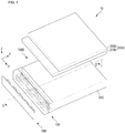
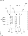
- FIG. 1 is a perspective view of a display device according to an embodiment of the present invention.
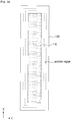
- FIG. 2 is a sectional view taken along the line II-II' of FIG. 1 .
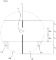
- FIG. 3A is an enlarged sectional view of portion A of FIG. 2 .
- FIG. 3B is a plane view of the first glass of FIG. 2
- the display device 10 includes a backlight unit 1000 and a display panel 2000 disposed (e.g., positioned) on the backlight unit 1000.
- the display panel 2000 may be an element capable of realizing image display (e.g., capable of displaying images).
- the display panel 2000 may be a liquid crystal display panel, an organic light-emitting display panel, a plasma display panel, or the like.
- the display panel 2000 may include a lower substrate 2100 and an upper substrate 2200 facing each other, and a liquid crystal layer interposed between the lower substrate 2100 and the upper substrate 2200.
- the lower substrate 2100 and the upper substrate 2200 may each independently include a plurality of pixel electrodes, a switching element for controlling the pixel electrodes, a gate line for transmitting a signal for controlling the switching element, and a data line.
- the planar area of the lower substrate 2100 may be larger than the planar area of the upper substrate 2200.
- the width of the lower substrate 2100 in the second direction Y may be greater than the width of the upper substrate 2200 in the second direction Y.
- the lower substrate 2100 may protrude toward a wavelength conversion member 100 as compared with the upper substrate 2200.
- the display panel 2000 and the backlight unit 1000 may be connected (or coupled) with each other using a connecting member.
- the backlight unit 1000 may be accommodated in a frame mold, and the display panel 2000 may be disposed on the frame mold or connected (coupled) with the frame mold.
- the backlight unit 1000 and the display panel 2000 may be connected with each other using a bonding resin.
- the backlight unit 1000 and the display panel 2000 may be connected with each other by bringing an upper surface of a light guide plate 200 of the backlight unit 1000 and a lower surface of the lower substrate 2100 of the display panel into direct contact with each other.
- the backlight unit 1000 includes the light guide plate 200, a light source unit 300 disposed adjacent to the light guide plate 200, and the wavelength conversion member 100 disposed between the light guide plate 200 and the light source unit 300.
- the light guide plate 200 may guide the light provided from the light source unit 300 and transmit the guided light toward the display panel 2000 located over the backlight unit 1000.
- the side surface of the light guide plate 200, adjacent to the light source unit 300 may form a light incoming surface
- the upper surface of the light guide plate 200 may form a light outgoing surface.
- the light incoming through the side face (the light incoming surface) of the light guide plate 200 may travel in the light guide plate 200 through total reflection, and at least a part of the light guided through the total reflection may leave through the upper surface (the light outgoing surface) of the light guide plate 200.
- a scattering pattern or a concavo-convex pattern may be formed on the lower surface of the light guide plate 200 to change the path of the light guided in the light guide plate 200.
- the material of the light guide plate 200 is not particularly limited as long as it is a material having high light transmittance and capable of guiding the light provided from the light source unit 300 without substantial light loss.
- the light guide plate 200 may be made of a glass material or a plastic material such as polycarbonate, polystyrene, and/or polyethylene terephthalate.
- the light source unit 300 may be disposed adjacent to the side surface (e.g., the light incoming surface) of the light guide plate 200.
- the light source unit 300 may be spaced apart from the light incoming surface of the light guide plate 200 by a set distance.
- the light source unit 300 may include a light source circuit substrate 310 and a light source 320 mounted on the light source circuit substrate 310.
- the light source circuit substrate 310 may be configured to be connected to an external power source or the like, in order to provide a signal and power necessary for driving the light source 320.
- the light source circuit board 310 may have a plate shape extending (elongated) in an approximately first direction X.
- the light source 320 may be disposed on the light source circuit board 310.
- a plurality of light sources 320 may be disposed on the light source circuit board 310 and the plurality of light sources 320 may be spaced apart from each other along the extension direction of the light source circuit board 310, for example, along the first direction X.
- the light source 320 may be a light emitting diode (LED).
- the light source 320 may be a light emitting diode that emits blue light.
- the light source 320 may emit blue light having a single peak wavelength located within a wavelength range of about 430 nm to 470 nm. About 80% or more of the light emitted by the light source 320 may be within a wavelength range of 430 nm to 470 nm.
- the light source 320 may be a light emitting diode that emits light in the ultraviolet wavelength band.
- the wavelength conversion member 100 may be disposed between the light guide plate 200 and the light source unit 300, for example, between the light guide plate 200 and the light source 320.
- the wavelength conversion member 100 may extend along a direction in which the plurality of light sources are arranged to be spaced apart from each other, for example, along the first direction X.
- the wavelength conversion member 100 may be spaced apart from the light source unit 300 by a predetermined (or set) distance. Since the wavelength conversion member 100 and the light source unit 300 are spaced apart from each other, it is possible to minimize (or reduce) the damage of a first wavelength converter 110 and a second wavelength converter 120 in the wavelength conversion member 100 that may result due to the heat emitted from the light source unit 300.
- the wavelength conversion member 100 may include a first wavelength converter 110 for converting the wavelength of transmitted light, a second wavelength converter 120 for converting the wavelength of transmitted light, a first glass 130 for providing a space for accommodating the first wavelength converter 110, and a second glass 140 for providing a space for accommodating the second wavelength converter 120.
- Each of the first wavelength converter 110 and the second wavelength converter 120 may convert the wavelength of the transmitted light.
- each of the first wavelength converter 110 and the second wavelength converter 120 may be a wavelength shifting member capable of shifting the peak wavelength of transmitted light.
- the first wavelength converter 110 may include a first base resin 110a and a first wavelength converting material 110b dispersed in the first base resin 110a, and may further include metal particles 110c dispersed in the first base resin 110a.
- the second wavelength converter 120 may include a second base resin 120a and a second wavelength converting material 120b dispersed in the second base resin 120a.
- the second wavelength converting material 120b may be different from the first wavelength converting material 110b.
- the first base resin 110a and the second base resin 120a may occupy most of the volume of the first wavelength converter 110 and the second wavelength converter 120, respectively.
- Each of the first base resin 110a and the second base resin 120a may be made of a material having high light transmittance and capable of uniformly dispersing the wavelength converting material and/or the metal particles.
- the first base resin 110a and the second base resin 120a may be made of the same or different materials.
- each of the first base resin 110a and the second base resin 120a may be a (meth)acrylate resin, an epoxy resin, a urethane resin, and/or a polyimide resin.
- Each of the first base resin 110a and the second base resin 120a may be a thermosetting resin or an ultraviolet curable resin.
- the first wavelength converting material 110b and the second wavelength converting material 120b may each emit light having a specific peak wavelength.
- each of the first wavelength converting material 110b and the second wavelength converting material 120b may be a material that converts incident light into light having a specific peak wavelength, and then emits the light.
- the first wavelength converting material 110b may emit red light
- the second wavelength converting material 120b may emit green light.
- Examples of the first wavelength converting material 110b and the second wavelength converting material 120b may include a fluorescent material and a quantum dot material, but are not limited thereto.
- the quantum dot material light having a specific peak wavelength can be emitted in the course of transferring electrons from the conduction band to the valence band.
- the quantum dot material may have a core-shell structure.
- the core may be a semiconductor nanocrystalline material. Examples of the core of the quantum dot material include Si-based nanocrystals, II-VI group-based compound nanocrystals, and III-V group-based compound nanocrystals, but the present invention is not limited thereto.
- each of the first wavelength converting material 110b and the second wavelength converting material 120b may include a core made of any one of cadmium selenide (CdSe), cadmium telluride (CdTe), cadmium sulfide (CdS), and indium phosphide (InP), and an outer shell made of zinc sulfide (ZnS).
- CdSe cadmium selenide
- CdTe cadmium telluride
- CdS cadmium sulfide
- InP indium phosphide
- ZnS zinc sulfide
- the average diameter of the particles of the first wavelength converting material 110b may be larger than the average diameter of the particles of the second wavelength converting material 120b.
- the average diameter of all the wavelength converting materials in the first wavelength converter 110 (if two or more first wavelength converting materials are included) may be about 55 ⁇ to 65 ⁇
- the average diameter of all the wavelength converting materials in the second wavelength converter 120 (if two or more second wavelength converting materials are included) may be about 40 ⁇ to 50 ⁇ .
- the wavelength converting material in the first wavelength converter 110 may be composed of only the first wavelength converting material 110b that emits red light
- the wavelength converting material in the second wavelength converter 120 may be composed of only the second wavelength converting material 120b that emits green light.
- the blue light emitted by the light source 320 may sequentially pass through the first wavelength converter 110 and the second wavelength converter 120.
- at least a part of the blue light emitted from the light source 320 may be converted into red light having a peak wavelength located within a wavelength range of about 610 nm to 650 nm by the first wavelength converter 110, and at least a part of the blue light emitted from the light source 320 may pass through the first wavelength converter 110 as it is (without being converted).
- At least a part of the light that passed through the first wavelength converter 110 may be further converted into green light having a peak wavelength located within a wavelength range of about 530 nm to 570 nm by the second wavelength converter 120, and at least a part of the light that passed through the first wavelength converter 110 may pass through the second wavelength converter 120 as it is (without being converted).
- the light converted by the first wavelength converter 110 and the second wavelength converter 120 may have a strong intensity peak wavelength in a narrow wavelength range, such light (after passing through the first wavelength converter 110 and the second wavelength converter 120) may have an intrinsic wavelength of a specific color and have excellent (or suitable) color purity.
- the light emitted by the light source 320 after passing through the wavelength conversion member 100, may be a high-purity white light only having a peak of a red intrinsic wavelength, a peak of a green intrinsic wavelength, and a peak of a blue intrinsic wavelength.
- the first wavelength converter 110 may further include metal particles 110c dispersed in the first base resin 110a.
- the metal particles 110c in the first wavelength converter 110 can further increase the color conversion efficiency of the wavelength conversion member 100.
- the metal particles 110c may be metal particles capable of scattering light in a long wavelength band such as green light and/or red light, without substantially scattering light in a short wavelength band such as blue light.
- the metal particles 110c may be aluminum oxide (Al 2 O 3 ) particles and/or silicon oxide (SiO 2 ) particles.
- the average diameter of the metal particles 110c may be about 10 ⁇ m to 100 ⁇ m.
- the metal particles 110c that do not substantially scatter light in a short wavelength band.
- the metal particles When such metal particles are disposed (placed) in the first wavelength converter 110, they may cause the scattering of red light emitted by the first wavelength converting material 110b, while also ensuring that a sufficient amount of blue light can pass through the first wavelength converter 110, without wavelength conversion, and can then be converted into green light by the second wavelength converter 120.
- the second wavelength converter 120 may include only the second base resin 120a and the second wavelength converting material 120b, without substantially including the metal particles.
- Each of the first wavelength converter 110 and the second wavelength converter 120 may have a thickness t 110 in the third direction Z, and the thickness t 110 of each of the first wavelength converter 110 and the second wavelength converter 120 may be greater than a width W 320 of the light-emitting surface of the light source 320 in the third direction Z.
- the width W 320 of the light source 320 may be about 1.5 mm to 2.5 mm
- the thickness t 110 of each of the first wavelength converter 110 and the second wavelength converter 120 may be about 2.5 mm to 4 mm.
- the first glass 130 and the second glass 140 may each be a container member capable of accommodating the first wavelength converter 110 and the second wavelength converter 120, respectively.
- Each of the first glass 130 and the second glass 140 may have a tubular shape having an inner hollow structure and extending in the first direction X, and each of the first wavelength converter 110 and the second wavelength converter 120 may be inserted into the hollow structure.
- FIG. 1 illustrates a case where the first wavelength converter 110 and the second wavelength converter 120 extend in the first direction X, and the wavelength conversion member 100 comprises one of each, but, in another embodiment, the plurality of first wavelength converters 110 and/or the plurality of second wavelength converters 120 may be arranged in the first direction X and spaced apart from each, for example, so as to be arranged at positions corresponding to the light sources 320.
- Each of the first glass 130 and the second glass 140 may be made of a glass material having relatively high light transmittance.
- the first glass 130 and the second glass 140 may be made of the same material or different materials.
- the first wavelength converter 110 may be accommodated by the first glass 130. On a sectional view taken along a direction perpendicular to the extending direction of the wavelength conversion member 100 (here, perpendicular to the first direction X), the first wavelength converter 110 may be completely surrounded by the first glass 130. With such arrangement, it may be possible to prevent or reduce the possibility of the first wavelength converter 110 from being contaminated and/or denatured by external moisture or impurities, and to improve the durability and lifetime of the wavelength conversion member 100.
- the second wavelength converter 120 may be accommodated by the second glass 140.
- the second wavelength converter 120 On a sectional view taken along a direction perpendicular to the extending direction of the wavelength conversion member 100 (here, perpendicular to the first direction X), the second wavelength converter 120 may be completely surrounded by the second glass 140. With such arrangement, it may be possible to prevent or reduce the possibility of the second wavelength converter 120 from being contaminated and/or denatured by external moisture or impurities, and to improve the durability and lifetime of the wavelength conversion member 100.
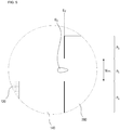
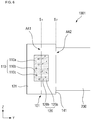
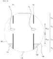
- FIG. 4 is an enlarged sectional view of portion B (a portion where the first glass 130 and the second glass 140 are connected or coupled) of FIG. 3A .
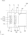
- FIG. 5 is an enlarged sectional view of portion C (a portion where the second glass 140 and the light guide plate 200 are connected or coupled) of FIG. 3A .
- the first glass 130 and the second glass 140 may be connected or coupled to be at least partially in direct contact with each other.
- the first glass 130 and the second glass 140 may be at least partially fusion-bonded to each other.
- the first glass 130 and the second glass 140 may be integrated (e.g., coupled) by at least partial fusion-bonding.
- fusion-bonded may refer to two materials being integrally connected or coupled to each other by, for example, welding.
- the contact surface S 1 between the first glass 130 and the second glass 140 includes a first portion P 1 where there is a physical boundary between the first glass 130 and the second glass 140, a second portion P 2 where there is substantially no physical boundary between the first portion 130 and the second glass 140, and a third portion P 3 overlapping the first and second wavelength converters 110 and 120 in the second direction Y.
- substantially no physical boundary between two components may refer to there being no naked-eye distinguishable boundary.
- the second portion P 2 may be a junction region between the first glass 130 and the second glass 140.
- the glass material of the first glass 130 and the glass material of the second glass 140 may be at least partially mixed, and thus the boundary between the first glass 130 and the second glass 140 may disappear.
- at least a part of the glass material of the first glass 130 may penetrate into the second glass 140 to be mixed with the glass material of the second glass 140, and/or at least a part of the glass material of the second glass 140 may penetrate into the first glass 130 to be mixed with the glass material of the first glass 130.
- the width W P2 of the second portion P 2 of the contact surface S 1 between the first glass 130 and the second glass 140 may refer to the width of the junction region and may be 60 ⁇ m to 120 ⁇ m, or 70 ⁇ m to 100 ⁇ m.
- the term "junction" may refer to a region in which two components are in direct contact with each other.
- a seed-like structure D 1 may exist in the vicinity of the second portion P 2 .
- the seed-like structure D 1 may be formed in the process of joining the first glass 130 and the second glass 140 together.
- the first glass 130 and the second glass 140 may be joined using a laser having a pulse width of about 10 femtoseconds to 50 femtoseconds.
- the pulse width of the laser is set within the above range, even when the first glass 130 and/or the second glass 140 is irradiated with the laser to allow the laser to pass through the first glass 130 and/or the second glass 140, it is possible to prevent or reduce the possibility of the other parts of the glass, other than the intended junction region, from being deformed in shape, structure, physical properties, density of the glass material, and/or the like, thereby improving the reliability and durability of the backlight unit.
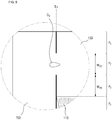
- the seed-like structure D 1 may have an elongated shape having a major axis (e.g., abscissa axis illustrated in the drawing) and a minor axis (e.g., ordinate axis illustrated in the drawing).
- the seed-like structure D 1 may be asymmetric with respect to the minor axis.
- the seed-like structure D 1 may be in a state in which the minor axis is aligned in a direction parallel to the contact surface S 1 , but the present invention is not limited thereto.
- the length of the minor axis of the seed-like structure D 1 may be about 10 ⁇ m to 20 ⁇ m.
- the first portion P 1 , the second portion P 2 , and the third portion P 3 may be located at substantially the same level (e.g., substantially aligned along the third direction Z), where the first portion P 1 may be located between the second portion P 2 and the third portion P 3 .
- the second portion P 2 where there is substantially no physical boundary between the first glass 130 and the second glass 140 (i.e. the junction region) may be spaced apart from the first wavelength converter 110 and the second wavelength converter 120 in the third direction Z.
- the shortest distance in the third direction Z (W P1 ) between the second portion P 2 and each of the first wavelength converter 110 and the second wavelength converter 120 may be about 50 ⁇ m or more.
- the width of the first portion P 1 may be about 50 ⁇ m or more.
- the second portion P 2 is spaced apart from the wavelength converters by 50 ⁇ m or more, it may be possible to prevent or reduce the possibility of the first wavelength converter 110 and/or the second wavelength converter 120 from being damaged by the high-temperature heat generated in the process of joining the first glass 130 and the second glass 140.
- the first portion P 1 and the second portion P 2 may differ from each other in terms of light transmittance, refractive index, and/or density of glass material.
- the wavelength conversion member 100 includes a first glass 130 for accommodating/sealing the first wavelength converter 110 and a second glass 140 for accommodating/sealing the second wavelength converter 120, and the first glass 130 and the second glass 140 are formed as an integrated module, thereby converting the light provided from the light source 320 into high-purity white light.
- the first wavelength converter 110 which may be a red wavelength conversion member
- the second wavelength converter 120 which may be a green wavelength conversion member
- the first wavelength converter 110 which may be a red wavelength conversion member
- the second wavelength converter 120 which may be a green wavelength conversion member
- first glass 130 accommodating the first wavelength converter 110 and the second glass 140 accommodating the second wavelength converter 120 are arranged to be at least partially in direct contact with each other without physical boundary, no (or reduced) deformation occurs in the junction region between the first glass 130 and the second glass 140, even when the wavelength conversion member 100 is heated by the heat emitted from the light source 320, thereby improving durability and reliability.
- the wavelength conversion member 100 and the light guide plate 200 may be connected to be at least partly in direct contact with each other.
- the second glass 140 of the wavelength conversion member 100 and the light-incoming surface of the light guide plate 200 may be at least partially fusion-bonded to each other. That is, the wavelength conversion member 100 and the light guide plate 200 may be integrated by at least partial fusion-bonding.
- the contact surface S 2 between the second glass 140 and the light guide plate 200 may include a fourth portion P 4 where there is a physical boundary between the second glass 140 and the light guide plate 200 and a fifth portion P 5 where there is substantially no physical boundary between the second glass 140 and the light guide plate 200.
- the fifth portion P 5 may be a junction region between the second glass 140 and the light guide plate 200.
- the width W P5 of the fifth portion P 5 (in the third direction Z) of the contact surface S 2 between the second glass 140 and the light guide plate 200 (i.e. the width of the junction region) may be 60 ⁇ m to 120 ⁇ m, or 70 ⁇ m to 100 ⁇ m.
- a seed-like structure D 2 may exist in the vicinity of the fifth portion P 5 .
- the seed-like structure D 2 may be formed in the process of joining the second glass 140 and the light guide plate 200 together.
- the second glass 140 and the light guide plate 200 may be joined using a laser having a pulse width of about 10 femtoseconds to 50 femtoseconds.
- the seed-like structure D 2 may have an elongated shape having a major axis and a minor axis.
- the seed-like structure D 2 may be asymmetric with respect to the minor axis.
- the length of the minor axis of the seed-like structure D 2 may be about 10 ⁇ m to 20 ⁇ m.
- the fourth portion P 4 and the fifth portion P 5 may be located at substantially the same level (e.g., substantially aligned along the third direction Z), and the fifth portion P 5 may not overlap the second wavelength converter 120 in the second direction Y.
- the fifth portion P 5 where there is substantially no physical boundary between the second glass 140 and the light guide plate 200 (i.e. the junction region) may not overlap the second wavelength converter 120 in a sectional view (e.g., as illustrated in FIG. 5 ). Since the fifth portion P 5 and the second wavelength converter 120 do not overlap each other, it may be possible to prevent or reduce the possibility that the laser beam used in the process of joining the first glass 130 and the second glass 140 may pass through the second wavelength converter 120 and damage the second wavelength converter 120.
- the fourth portion P 4 and the fifth portion P 5 may differ from each other in terms of light transmittance, refractive index, and/or density of glass material.
- the backlight unit 1000 may be configured such that the wavelength conversion member 100 accommodating the plurality of wavelength converters is integrated with the light guide plate 200 to form a module.
- the backlight unit 1000 or the display device including the backlight unit 1000 it may be possible to prevent or reduce the misalignment between the wavelength conversion member 100 and the light guide plate 200, and thus it may be possible to prevent or reduce the possibility of the light emitted from the light source 320 from being incident on the light guide plate 200 without first passing through the wavelength conversion member 100. Further, it may be possible to prevent or reduce the possibility of the light passing through the wavelength conversion member 100 and from being leaked without being incident on the light guide plate 200.
- the wavelength conversion member 100 accommodating the plurality of wavelength converters and the light guide plate 200 are connected to be at least partially in direct contact with each other without physical boundary, deformation that may otherwise occur in the junction region between the wavelength conversion member 100 and the light guide plate 200 may be prevented or reduced, even when the wavelength conversion member 100 and the light guide plate 200 are heated by the heat emitted from the light source 320.
- the durability and reliability of the backlight unit 1000 may be improved.
- FIG. 6 is an enlarged sectional view of a backlight unit according to another embodiment of the present invention.
- a backlight unit 1001 includes a wavelength conversion member 101 including a first wavelength converter 110, a second wavelength converter 120, a first glass 131 providing a space for accommodating the first wavelength converter 110, and a second glass 141 providing a space for accommodating the second wavelength converter 120.
- the backlight unit 1001 according to this embodiment is different from the backlight unit 1000 according to the embodiment of FIG. 1 in that trench-shaped concave grooves extending in the first direction X are formed on any one side of the first glass 131 and the second glass 141, and the first wavelength converter 110 and the second wavelength converter 120 are inserted into the concave grooves.
- Each of the first wavelength converter 110 and the second wavelength converter 120 may convert the wavelength of transmitted light.
- the first wavelength converter 110 may be a red wavelength converter
- the second wavelength converter 120 may be a green wavelength converter. Since the first wavelength converter 110 and the second wavelength converter 120 have been described above with reference to, for example, FIG. 1 , a detailed description thereof will not be provided again.
- the first glass 131 and the second glass 141 may be container members that accommodate the first wavelength converter 110 and the second wavelength converter 120, respectively.
- one side (right side in the drawing) of the first glass 131, facing the second glass 141 may have a concave groove extending along the extension direction of the wavelength conversion member 1001 (e.g., along the first direction X), and the other side (left side in the drawing) of the second glass 141, facing the first glass 131, may have a concave groove extending along the first direction X.
- the first wavelength converter 110 and the second wavelength converter 120 may be inserted into the concave grooves of the first glass 131 and the second glass 141, respectively.
- the first wavelength converter 110 and the second wavelength converter 120 may directly face each other, and may be at least partially in direct contact with each other.
- the first wavelength converter 110 and the second wavelength converter 120 may be accommodated by the first glass 131 and the second glass 141, respectively.
- the first glass 131 and the second glass 141 may be at least partially in direct contact with each other.
- the first glass 131 and the second glass 141 may be at least partially fusion-bonded to each other.
- the contact surface S 1 between the first glass 131 and the second glass 141 may include a portion where there is substantially no physical boundary therebetween (herein, referred to as a junction region AA1). Since the junction region AA1 between the first glass 131 and the second glass 141 is substantially similar to the junction region between the first glass 130 and the second glass 140 described above with reference to FIG. 4 and the like, a detailed description thereof will not be provided again.
- the wavelength conversion member 101 and the light guide plate 200 may be at least partially in direct contact with each other.
- the second glass 141 of the wavelength conversion member 101 and the light incoming surface of the light guide plate 200 may be at least partially fusion-bonded to each other.
- the contact surface S 2 between the second glass 141 and the light guide plate 200 may include a portion where there is substantially no physical boundary therebetween (herein, referred to as a junction region AA2). Since the junction region AA2 between the second glass 141 and the light guide plate 200 is substantially similar to the junction region between the second glass 140 and the light guide plate 200 described above with reference to FIG. 5 and the like, a detailed description thereof will not be provided again.
- FIG. 7 is an enlarged sectional view of a backlight unit according to another embodiment of the present invention.
- a backlight unit 1002 includes a wavelength conversion member 102 including a first wavelength converter 112 and a second wavelength converter 122.
- the backlight unit 1002 according to this embodiment is different from the backlight unit 1001 according to the embodiment of FIG. 6 in that there is a gap AG formed between the first wavelength converter 112 and the second wavelength converter 122.
- the first wavelength converter 112 is inserted into the concave groove of the first glass 131, but the first wavelength converter 112 may not completely fill the concave groove of the first glass 131. That is, the volume occupied by the first wavelength converter 112 may be smaller than the volume of the space provided by the concave groove of the first glass 131. Further, the second wavelength converter 122 is inserted into the concave groove of the second glass 141, but the first wavelength converter 112 may not completely fill the concave groove of the second glass 141.
- nitrogen gas (N 2 ) or an air layer may be interposed in the gap AG.
- the gap AG may form a low refractive index region having a lower refractive index than those of the first wavelength conversion unit 112, the second wavelength conversion unit 122, the first glass 131, and the second glass 141.
- the red light and blue light that pass through the first wavelength converter 112 may then pass through the gap AG, a low refractive index region, before passing through the second wavelength converter 122, thereby maximizing photo-excitation efficiency.
- the color conversion efficiency can be further improved by forming the gap AG between the first wavelength converter 112 and the second wavelength converter 122.
- a light outgoing direction may be controlled..
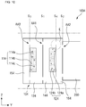
- FIG. 8 is an enlarged sectional view of a backlight unit according to another embodiment of the present invention.
- FIG. 9 is an enlarged sectional view of portion D of FIG. 8 .
- a backlight unit 1003 includes a wavelength conversion member 103 including a first wavelength converter 113, a second wavelength converter 123, a first glass 133 providing a space for accommodating the first wavelength converter 113, and a second glass 143 providing a space for accommodating the second wavelength converter 123.
- the backlight unit 1003 according to this embodiment is different from the backlight unit 1000 according to the embodiment of FIG. 1 and the like in that it further includes a third glass 153 sealing the first wavelength converter 113.
- Each of the first wavelength converter 113 and the second wavelength converter 123 may convert the wavelength of transmitted light.
- the first wavelength converter 113 may be a red wavelength converter
- the second wavelength converter 123 may be a green wavelength converter. Since the first wavelength converter 113 and the second wavelength converter 123 are substantially similar to the first wavelength converter 110 and the second wavelength converter 120, respectively, that have been described with reference to FIG. 1 and the like, a detailed description thereof will not be provided again.
- the first glass 133 and the second glass 143 may be container members that accommodate the first wavelength converter 113 and the second wavelength converter 123, respectively, and the third glass 153 may be a cover member sealing the first wavelength converter 113.
- one side (right side in the drawing) of the third glass 153, facing the first glass 133 may be substantially flat.
- the side of the first glass 133 facing the third glass 153 (left side in the drawing) may have a concave groove
- the side of the second glass 143 facing the first glass 133 (left side in the drawing) may have a concave groove.
- the first wavelength converter 113 may be inserted into the concave groove of the first glass 133, and may be completely surrounded by the first glass 133 and the third glass 153.
- the second wavelength converter 123 may be inserted into the concave groove of the second glass 143, and may completely surrounded by the first glass 133 and the second glass 143.
- the first glass 133 and the third glass 153 may be at least partially in direct contact with each other.
- the first glass 133 and the third glass 153 may be at least partially fusion-bonded to each other.
- the contact surface S 3 between the first glass 133 and the third glass 153 includes a sixth portion P 6 where there is a physical boundary between the first glass 133 and the third glass 153, a seventh portion P 7 where there is substantially no physical boundary between the first glass 133 and the third glass 153, and an eighth portion P 8 overlapping the first wavelength converter 113 in the second direction Y.
- the width W P7 of the seventh portion P 7 of the contact surface S 3 between the first glass 133 and the third glass 153 may be 60 ⁇ m to 120 ⁇ m, or 70 ⁇ m to 100 ⁇ m.
- a seed-like structure D 3 may exist in the vicinity of the seventh portion P 7 .
- the seed-like structure D 3 may be formed in the process of joining the first glass 133 and the third glass 153 together.
- the first glass 133 and the third glass 153 may be joined using a laser having a pulse width of about 10 femtoseconds to 50 femtoseconds.
- the seed-like structure D 3 may have an elongated shape having a major axis and a minor axis.
- the seed-like structure D 3 may be asymmetric with respect to the minor axis.
- the length of the minor axis of the seed-like structure D 3 may be about 10 ⁇ m to 20 ⁇ m.
- the sixth portion P 6 , the seventh portion P 7 , and the eighth portion P 8 may be located at substantially the same level (e.g., substantially aligned along the third direction Z), and the sixth portion P 6 may be located between the seventh portion P 7 and the eighth portion P 8 .
- the seventh portion P 7 between the first glass 133 and the third glass 153 i.e. the junction region
- the shortest distance W P6 (in the third direction Z) between the seventh portion P 7 and the first wavelength converter 113 may be about 50 ⁇ m or more.
- junction region AA1 between the first glass 133 and the second glass 143 and the junction region AA2 between the second glass 143 and the light guide plate 200 have been described above with reference to FIGS. 4 and 5 , a detailed description thereof will not be provided again.
- FIG. 8 illustrates a case where a gap is formed between the first wavelength converter 113 and the third glass 153, and a gap is formed between the second wavelength converter 123 and the first glass 133.
- the first wavelength converter 113 may completely fill a space between the first glass 133 and the third glass 153 (e.g., there may be no gap between the the first wavelength converter 113 and the third glass 153)
- the second wavelength converter 123 may completely fill a space between the first glass 133 and the second glass 143 (e.g., there may be no gap between the second wavelength converter 123 and the first glass 133).
- FIG. 10 is an enlarged sectional view of a backlight unit according to another embodiment of the present invention.
- FIG. 11 is an enlarged sectional view of portion E of FIG. 10 .
- a backlight unit 1004 includes a wavelength conversion member 104 including a first wavelength converter 114, a second wavelength converter 124, a first glass 134 providing a space for accommodating the first wavelength converter 114, and a second glass 144 providing a space for accommodating the second wavelength converter 124.
- the backlight unit 1004 according to this embodiment is different from the backlight unit 1000 according to the embodiment of FIG. 1 and the like in that it further include a third glass 154 sealing the first wavelength converter 114 and a fourth glass 164 sealing the second wavelength converter 124.
- Each of the first wavelength converter 114 and the second wavelength converter 124 may convert the wavelength of transmitted light.
- the first wavelength converter 114 may be a red wavelength converter
- the second wavelength converter 124 may be a green wavelength converter. Since the first wavelength converter 114 and the second wavelength converter 124 are substantially similar to the first wavelength converter 110 and the second wavelength converter 120, respectively, that have been described above with reference to FIG. 1 and the like, a detailed description thereof will not be provided again.
- the first glass 134 and the second glass 144 may be container members that accommodate the first wavelength converter 114 and the second wavelength converter 124, respectively, and the third glass 154 and the fourth glass 164 may be cover members sealing the first wavelength converter 114 and the second wavelength converter 124, respectively.
- one side of the third glass 154 facing the first glass 134 may be substantially flat.
- the side of the first glass 134 facing the third glass 154 may have a concave groove, and the other side of the first glass 134, facing the second glass 144 (right side in the drawing), may be substantially flat.
- the side of the second glass 144 facing the fourth glass 164 may have a concave groove
- the other side of the fourth glass 164, facing the second glass 144 may be substantially flat.
- the first wavelength converter 114 may be inserted into the concave groove of the first glass 134, and may be completely surrounded by the first glass 134 and the third glass 154.
- the second wavelength converter 124 may be inserted into the concave groove of the second glass 144, and may be completely surrounded by the second glass 144 and the fourth glass 164.
- the light guide plate 200 may be at least partially in direct contact with the fourth glass 164, instead of the second glass 144.
- the second glass 144 and the fourth glass 164 may be at least partially in direct contact with each other.
- the second glass 144 and the fourth glass 164 may be at least partially fusion-bonded to each other.
- the contact surface S 4 between the second glass 144 and the fourth glass 164 may include a ninth portion P 9 where there is a physical boundary between the second glass 144 and the fourth glass 164, a tenth portion P 10 where there is substantially no physical boundary between the second glass 144 and the fourth glass 164, and an eleventh portion P 11 overlapping the second wavelength converter 124 in the second direction Y.
- the width W P10 of the tenth portion P 10 of the contact surface S 4 between the second glass 144 and the fourth glass 164 (herein, the tenth portion P 10 may be referred to as the junction region) may be 60 ⁇ m to 120 ⁇ m, or 70 ⁇ m to 100 ⁇ m.
- a seed-like structure D 4 may exist in the vicinity of the tenth portion P 10 .
- the seed-like structure D 4 may be formed in the process of joining the second glass 144 and the fourth glass 164 together.
- the second glass 144 and the fourth glass 164 may be joined using a laser having a pulse width of about 10 femtoseconds to 50 femtoseconds.
- the seed-like structure D 4 may have an elongated shape having a major axis and a minor axis.
- the seed-like structure D 4 may be asymmetric with respect to the minor axis.
- the length of the minor axis of the seed-like structure D 4 may be about 10 ⁇ m to 20 ⁇ m.
- the ninth portion P 9 , the tenth portion P 10 , and the eleventh portion P 11 may be located at substantially the same level (e.g., substantially aligned along the third direction Z), and the ninth portion P 9 may be located between the tenth portion P 10 and the eleventh portion P 11 .
- the tenth portion P 10 between the second glass 144 and the fourth glass 164 (the junction region) may be spaced apart from the second wavelength converter 124 in the third direction Z.
- the shortest distance W P9 (in the third direction Z) between the tenth portion P 10 and the second wavelength converter 124 may be about 50 ⁇ m or more.
- junction region AA1 between the first glass 134 and the second glass 144, the junction region AA2 between the fourth glass 164 and the light guide plate 200, and the junction region AA3 between the first glass 134 and the third glass 154 are substantially similar to the corresponding junction regions described above (e.g., with reference to FIGS. 4 , 5 , and 8 ), a detailed description thereof will not be provided again.
- FIG. 10 illustrates a case where a gap is formed between the first wavelength converter 114 and the third glass 154 and a gap is formed between the second wavelength converter 124 and the fourth glass 164
- the first wavelength converter 114 may completely fill a space between the first glass 134 and the third glass 154 (e.g., there may be no gap between the first wavelength converter 114 and the third glass 154)
- the second wavelength converter 124 may completely fill a space between the second glass 144 and the fourth glass 164 (e.g., there may be no gap between the second wavelength converter 124 and the fourth glass 164).
- FIG. 12 is an enlarged sectional view of a backlight unit according to another embodiment of the present invention.
- a backlight unit 1005 according to this embodiment is different from the backlight unit 1004 according to the embodiment of FIG. 10 and the like in that a first wavelength converter 115 and a second wavelength converter 125 of a wavelength conversion member 105 are both inserted in one first glass 135.
- the first glass 135 may be a container member that accommodates the first wavelength converter 115 and the second wavelength converter 125, and the third glass 155 and the fourth glass 165 may be cover members sealing the first wavelength converter 115 and the second wavelength converter 125.
- the first glass 135 may be integrally formed.
- the light transmittance, refractive index and/or density of a glass material in the first glass 135 may be uniform.
- the side of the third glass 155 facing the first glass 135 may be substantially flat. Further, the side of the first glass 135 facing the third glass 155 (left side in the drawing), and the side of the first glass 135 facing the fourth glass 165 (right side in the drawing), may have concave grooves, respectively. Further, the side of the fourth glass 165 facing the first glass 135 (left side in the drawing), may be substantially flat.
- the first wavelength converter 115 may be inserted into the concave groove of the side of the first glass 135 facing the third glass 155, and the second wavelength converter 125 may be inserted into the concave groove of the side of the first glass 135 facing the fourth glass 165.
- the first wavelength converter 115 may be surrounded by the first glass 135 and the third glass 155 and the second wavelength converter 125 may be surrounded by the first glass 135 and the fourth glass 165.
- junction region AA2 between the fourth glass 165 and the light guide plate 200 Since the junction region AA2 between the fourth glass 165 and the light guide plate 200, the junction region AA3 between the first glass 135 and the third glass 155, and the junction region AA4 between the first glass 135 and the fourth glass 165 are substantially similar to the corresponding junction regions that have been described above (e.g., with reference to FIGS. 5 , 8 , and 10 ), a detailed description thereof will not be provided again.
- FIG. 13 is an enlarged sectional view of a backlight unit according to another embodiment of the present invention.
- FIG. 14 is an enlarged sectional view of portion F of FIG. 13 .
- a backlight unit 1006 includes a wavelength conversion member 106 including a first wavelength converter 116, a second wavelength converter 126, a first glass 136 providing a space for accommodating the first wavelength converter 116, and a second glass 146 providing a space for accommodating the second wavelength converter 126.
- the backlight unit 1006 according to this embodiment is different from the backlight unit 1001 according to the embodiment of FIG. 6 and the like in that it further includes a fifth glass 176 interposed (positioned) between the first wavelength converter 116 and the second wavelength converter 126.
- the first glass 136 and the second glass 146 may be container members that accommodate the first wavelength converter 116 and the second wavelength converter 126, respectively, and the fifth glass 176 may be a spacer member that spaces the first wavelength converter 116 and the second wavelength converter 126 from each other by a predetermined (or set) distance.
- the side of the first glass 136 facing the fifth glass 176 may have a concave groove extending along the extension direction of the wavelength conversion member 106 (here, along the first direction X), and the side of the second glass 146 facing the fifth glass 176 (left side in the drawing), may have a concave groove extending along the first direction X.
- both the side of the fifth glass 176 facing the first glass 136 (left side in the drawing) and the side of the fifth glass 176 facing the second glass 146 (right side in the drawing) may be substantially flat.
- the first wavelength converter 116 and the second wavelength converter 126 may be inserted into the respective concave grooves.
- the first wavelength converter 116 may be surrounded by the first glass 136 and the fifth glass 176
- the second wavelength converter 126 may be surrounded by the second glass 146 and the fifth glass 176.
- first glass 136 and the fifth glass 176 may be at least partially in direct contact with each other, and the second glass 146 and the fifth glass 176 may be at least partially in direct contact with each other.
- first glass 136 and the fifth glass 176 may be at least partially fusion-bonded to each other, and the second glass 146 and the fifth glass 176 may be at least partially fusion-bonded to each other.
- the contact surface S 5 between the first glass 136 and the fifth glass 176 and the contact surface S 6 between the second glass 146 and the fifth glass 176 may each include, in the second direction Y, a twelfth portion P 12 where there is a physical boundary between the respective adjacent glasses, a thirteenth portion P 13 where there is substantially no physical boundary between the respective adjacent glasses, and a fourteenth portion P 14 overlapping the wavelength converters 116 and 126.
- the width W P13 of the thirteenth portion P 13 (herein, the thirteenth portion P 13 may be referred to as the junction region) may be 60 ⁇ m to 120 ⁇ m, or 70 ⁇ m to 100 ⁇ m.
- Seed-like structures D 5 and D 6 may exist in the vicinity of the thirteenth portion P 13 of the contact surface S 5 between the first glass 136 and the fifth glass 176 and in the vicinity of the thirteenth portion P 13 of the contact surface S 6 between the second glass 146 and the fifth glass 176, respectively.
- the seed-like structures D 5 and D 6 may be formed in the process of joining the respective adjacent glasses together.
- the first glass 136 and the fifth glass 176, and the second glass 146 and the fifth glass 176 may be joined using a laser having a pulse width of about 10 femtoseconds to 50 femtoseconds, respectively.
- Each of the seed-like structures D 5 and D 6 may have an elongated shape having a major axis and a minor axis.
- Each of the seed-like structures D 5 and D 6 may be asymmetric with respect to the minor axis.
- the length of the minor axis of each of the seed-like structures D 5 and D 6 may be about 10 ⁇ m to 20 ⁇ m.
- the wavelength conversion member according to an embodiment of the present invention can convert the light provided from a light source into high-purity white light.
- the backlight unit according to an embodiment of the present invention can provide high-purity white light using the wavelength conversion member, can minimize or reduce the light loss between a wavelength conversion member and a light guide plate by accurately maintaining the alignment state between the wavelength conversion member and the light guide plate, even when an external impact is applied, and can maximize or improve color conversion efficiency.
- any numerical range recited herein is intended to include all sub-ranges of the same numerical precision subsumed within the recited range.
- a range of "1.0 to 10.0" is intended to include all subranges between (and including) the recited minimum value of 1.0 and the recited maximum value of 10.0, that is, having a minimum value equal to or greater than 1.0 and a maximum value equal to or less than 10.0, such as, for example, 2.4 to 7.6.
- Any maximum numerical limitation recited herein is intended to include all lower numerical limitations subsumed therein and any minimum numerical limitation recited in this specification is intended to include all higher numerical limitations subsumed therein. Accordingly, Applicant reserves the right to amend this specification, including the claims, to expressly recite any sub-range subsumed within the ranges expressly recited herein.
Landscapes
- Physics & Mathematics (AREA)
- Engineering & Computer Science (AREA)
- Nonlinear Science (AREA)
- Optics & Photonics (AREA)
- General Physics & Mathematics (AREA)
- Chemical & Material Sciences (AREA)
- Microelectronics & Electronic Packaging (AREA)
- Mathematical Physics (AREA)
- Crystallography & Structural Chemistry (AREA)
- Power Engineering (AREA)
- Computer Hardware Design (AREA)
- Manufacturing & Machinery (AREA)
- Organic Chemistry (AREA)
- Materials Engineering (AREA)
- Inorganic Chemistry (AREA)
- General Engineering & Computer Science (AREA)
- Astronomy & Astrophysics (AREA)
- Spectroscopy & Molecular Physics (AREA)
- Liquid Crystal (AREA)
- Optical Filters (AREA)
Applications Claiming Priority (1)
| Application Number | Priority Date | Filing Date | Title |
|---|---|---|---|
| KR1020170010302A KR20180087487A (ko) | 2017-01-23 | 2017-01-23 | 파장 변환 부재 및 이를 포함하는 백라이트 유닛 |
Publications (2)
| Publication Number | Publication Date |
|---|---|
| EP3352004A1 true EP3352004A1 (de) | 2018-07-25 |
| EP3352004B1 EP3352004B1 (de) | 2021-04-21 |
Family
ID=61002878
Family Applications (1)
| Application Number | Title | Priority Date | Filing Date |
|---|---|---|---|
| EP18152028.9A Active EP3352004B1 (de) | 2017-01-23 | 2018-01-17 | Wellenlängenumwandlungselement und rückbeleuchtungseinheit damit |
Country Status (4)
| Country | Link |
|---|---|
| US (1) | US10386024B2 (de) |
| EP (1) | EP3352004B1 (de) |
| KR (1) | KR20180087487A (de) |
| CN (1) | CN108346734B (de) |
Cited By (1)
| Publication number | Priority date | Publication date | Assignee | Title |
|---|---|---|---|---|
| EP3330786A3 (de) * | 2016-11-30 | 2018-09-12 | Samsung Display Co., Ltd. | Rückbeleuchtungseinheit, anzeige und herstellungsverfahren der anzeigevorrichtung |
Families Citing this family (2)
| Publication number | Priority date | Publication date | Assignee | Title |
|---|---|---|---|---|
| KR20180083011A (ko) * | 2017-01-11 | 2018-07-20 | 삼성디스플레이 주식회사 | 광원 유닛, 이를 포함하는 표시 장치 및 표시 장치의 제조 방법 |
| CN115629497A (zh) * | 2017-04-03 | 2023-01-20 | 英特曼帝克司公司 | 彩色液晶显示器及显示器背光 |
Citations (4)
| Publication number | Priority date | Publication date | Assignee | Title |
|---|---|---|---|---|
| WO2012105746A1 (en) * | 2011-01-31 | 2012-08-09 | Lg Innotek Co., Ltd. | Optical member and display device including the same |
| WO2013012193A2 (en) * | 2011-07-20 | 2013-01-24 | Lg Innotek Co., Ltd. | Optical member and display device having the same |
| US20160054503A1 (en) * | 2014-08-19 | 2016-02-25 | Shenzhen China Star Optoelectronics Technology Co. Ltd. | Backlight Module and Liquid Crystal Display Device |
| US20160139319A1 (en) * | 2014-11-14 | 2016-05-19 | Shenzhen China Star Optoelectronics Technology Co., Ltd. | Backlight module and liquid crystal display device |
Family Cites Families (27)
| Publication number | Priority date | Publication date | Assignee | Title |
|---|---|---|---|---|
| US6501091B1 (en) | 1998-04-01 | 2002-12-31 | Massachusetts Institute Of Technology | Quantum dot white and colored light emitting diodes |
| JP2006173324A (ja) * | 2004-12-15 | 2006-06-29 | Nichia Chem Ind Ltd | 発光装置 |
| US7356054B2 (en) * | 2004-12-17 | 2008-04-08 | Nichia Corporation | Light emitting device |
| US7682850B2 (en) * | 2006-03-17 | 2010-03-23 | Philips Lumileds Lighting Company, Llc | White LED for backlight with phosphor plates |
| EP2240819A1 (de) * | 2008-01-03 | 2010-10-20 | Koninklijke Philips Electronics N.V. | Anzeigevorrichtung und Beleuchtungsvorrichtung |
| TWI438262B (zh) * | 2008-02-07 | 2014-05-21 | Mitsubishi Chem Corp | A semiconductor light emitting device, a backlight, a color image display device, and a phosphor |
| KR101587529B1 (ko) * | 2008-03-07 | 2016-01-22 | 코닌클리케 필립스 엔.브이. | 컬러 가변 발광 장치 |
| KR100982991B1 (ko) * | 2008-09-03 | 2010-09-17 | 삼성엘이디 주식회사 | 양자점 파장변환체, 양자점 파장변환체의 제조방법 및 양자점 파장변환체를 포함하는 발광장치 |
| US8294168B2 (en) | 2010-06-04 | 2012-10-23 | Samsung Electronics Co., Ltd. | Light source module using quantum dots, backlight unit employing the light source module, display apparatus, and illumination apparatus |
| KR101210158B1 (ko) * | 2010-11-04 | 2012-12-07 | 엘지이노텍 주식회사 | 표시장치 및 광 변환 부재 |
| WO2012088404A1 (en) * | 2010-12-23 | 2012-06-28 | Qd Vision, Inc. | Quantum dot containing optical element |
| KR20120106012A (ko) * | 2011-03-17 | 2012-09-26 | 삼성전자주식회사 | 발광 소자 패키지 |
| WO2012135744A2 (en) * | 2011-04-01 | 2012-10-04 | Kai Su | White light-emitting device |
| CN202065823U (zh) * | 2011-05-13 | 2011-12-07 | 京东方科技集团股份有限公司 | 一种白光led及其器件 |
| KR101877489B1 (ko) | 2011-10-31 | 2018-07-13 | 엘지이노텍 주식회사 | 표시장치 |
| JP2013149729A (ja) * | 2012-01-18 | 2013-08-01 | Fujifilm Corp | 量子ドット構造体、波長変換素子および光電変換装置 |
| JP2014082416A (ja) * | 2012-10-18 | 2014-05-08 | Sharp Corp | 発光装置 |
| JP7068771B2 (ja) * | 2013-07-08 | 2022-05-17 | ルミレッズ ホールディング ベーフェー | 波長変換式半導体発光デバイス |
| EP3058401A4 (de) * | 2013-10-17 | 2017-05-17 | Nanosys, Inc. | Leuchtdioden (led)-vorrichtungen |
| US20150192272A1 (en) * | 2014-01-06 | 2015-07-09 | John S. Berg | System for producing color transformable light |
| WO2015121089A1 (en) * | 2014-02-11 | 2015-08-20 | Koninklijke Philips N.V. | A wavelength converting element, a light emitting module and a luminaire |
| CN105444045A (zh) * | 2014-09-24 | 2016-03-30 | 青岛海信电器股份有限公司 | 一种发光二极管led发光器件、背光模组及显示面板 |
| CN105444044A (zh) * | 2014-09-24 | 2016-03-30 | 青岛海信电器股份有限公司 | 一种发光二极管led发光器件、背光模组及显示面板 |
| JP2016072076A (ja) * | 2014-09-30 | 2016-05-09 | 日亜化学工業株式会社 | バックライト装置 |
| KR20170096173A (ko) * | 2014-12-22 | 2017-08-23 | 쓰리엠 이노베이티브 프로퍼티즈 컴파니 | 하향변환 필름 요소 |
| KR20160090453A (ko) * | 2015-01-21 | 2016-08-01 | 삼성디스플레이 주식회사 | 퀀텀 도트 패널, 라이트 유닛 및 이를 포함하는 표시 장치 |
| JP6422572B2 (ja) * | 2015-04-20 | 2018-11-14 | シャープ株式会社 | 照明装置、表示装置、及びテレビ受信装置 |
-
2017
- 2017-01-23 KR KR1020170010302A patent/KR20180087487A/ko active IP Right Grant
-
2018
- 2018-01-12 US US15/870,725 patent/US10386024B2/en not_active Expired - Fee Related
- 2018-01-17 EP EP18152028.9A patent/EP3352004B1/de active Active
- 2018-01-23 CN CN201810062709.2A patent/CN108346734B/zh active Active
Patent Citations (4)
| Publication number | Priority date | Publication date | Assignee | Title |
|---|---|---|---|---|
| WO2012105746A1 (en) * | 2011-01-31 | 2012-08-09 | Lg Innotek Co., Ltd. | Optical member and display device including the same |
| WO2013012193A2 (en) * | 2011-07-20 | 2013-01-24 | Lg Innotek Co., Ltd. | Optical member and display device having the same |
| US20160054503A1 (en) * | 2014-08-19 | 2016-02-25 | Shenzhen China Star Optoelectronics Technology Co. Ltd. | Backlight Module and Liquid Crystal Display Device |
| US20160139319A1 (en) * | 2014-11-14 | 2016-05-19 | Shenzhen China Star Optoelectronics Technology Co., Ltd. | Backlight module and liquid crystal display device |
Cited By (3)
| Publication number | Priority date | Publication date | Assignee | Title |
|---|---|---|---|---|
| EP3330786A3 (de) * | 2016-11-30 | 2018-09-12 | Samsung Display Co., Ltd. | Rückbeleuchtungseinheit, anzeige und herstellungsverfahren der anzeigevorrichtung |
| US10663647B2 (en) | 2016-11-30 | 2020-05-26 | Samsung Display Co., Ltd. | Backlight unit, display device and manufacturing method of display device |
| US11035999B2 (en) | 2016-11-30 | 2021-06-15 | Samsung Display Co., Ltd. | Backlight unit, display device and manufacturing method of display device |
Also Published As
| Publication number | Publication date |
|---|---|
| US10386024B2 (en) | 2019-08-20 |
| KR20180087487A (ko) | 2018-08-02 |
| CN108346734B (zh) | 2023-09-22 |
| EP3352004B1 (de) | 2021-04-21 |
| CN108346734A (zh) | 2018-07-31 |
| US20180210125A1 (en) | 2018-07-26 |
Similar Documents
| Publication | Publication Date | Title |
|---|---|---|
| US11621376B2 (en) | Light emitting device, light emitting diode package, backlight unit, and liquid crystal display | |
| US10451790B2 (en) | Lighting device, display device, and television device that reduce unevenness in displayed color | |
| US9223081B2 (en) | Optical member and display device including the same | |
| EP2734893B1 (de) | Anzeigevorrichtung | |
| EP2734894B1 (de) | Anzeigevorrichtung | |
| US9720160B2 (en) | Display device and optical member | |
| US9557467B2 (en) | Display device | |
| EP2734876B1 (de) | Optisches element zur wellenlängenkonversion und anzeigevorrichtung damit | |
| US20180095329A1 (en) | Lighting device, display device, and television device | |
| CN104040382A (zh) | 光学片以及具有该光学片的显示装置和发光装置 | |
| US10386024B2 (en) | Wavelength conversion member having two different wavelength converting materials and backlight unit including the same | |
| US10910447B2 (en) | Display device and method of manufacturing the same | |
| US11421856B2 (en) | Light emitting module, surface light source, and a method of manufacturing light emitting module | |
| US20190154901A1 (en) | Optical member and display including the same | |
| JP2018092025A (ja) | 照明装置及び表示装置 | |
| US9405051B2 (en) | Backlight assembly and display device having the same | |
| US20190221719A1 (en) | Backlight source | |
| US10578790B2 (en) | Light source unit, display device including the light source unit, and manufacturing method of the display device | |
| KR20160049082A (ko) | 액정 표시 장치 | |
| EP3699488B1 (de) | Anzeigevorrichtung | |
| CN108027117B (zh) | 照明装置、显示装置以及电视接收装置 | |
| KR20190087069A (ko) | 발광 소자 장치 및 이를 포함하는 백라이트 유닛 | |
| US20220382106A1 (en) | Light emitting module and optical lens thereof | |
| US20190170924A1 (en) | Backlight unit having a light guide plate with a patterned capping layer and display device including the same | |
| CN117080349A (zh) | 发光模块和发光模块的制造方法 |
Legal Events
| Date | Code | Title | Description |
|---|---|---|---|
| PUAI | Public reference made under article 153(3) epc to a published international application that has entered the european phase |
Free format text: ORIGINAL CODE: 0009012 |
|
| STAA | Information on the status of an ep patent application or granted ep patent |
Free format text: STATUS: THE APPLICATION HAS BEEN PUBLISHED |
|
| AK | Designated contracting states |
Kind code of ref document: A1 Designated state(s): AL AT BE BG CH CY CZ DE DK EE ES FI FR GB GR HR HU IE IS IT LI LT LU LV MC MK MT NL NO PL PT RO RS SE SI SK SM TR |
|
| AX | Request for extension of the european patent |
Extension state: BA ME |
|
| STAA | Information on the status of an ep patent application or granted ep patent |
Free format text: STATUS: REQUEST FOR EXAMINATION WAS MADE |
|
| 17P | Request for examination filed |
Effective date: 20180903 |
|
| RBV | Designated contracting states (corrected) |
Designated state(s): AL AT BE BG CH CY CZ DE DK EE ES FI FR GB GR HR HU IE IS IT LI LT LU LV MC MK MT NL NO PL PT RO RS SE SI SK SM TR |
|
| STAA | Information on the status of an ep patent application or granted ep patent |
Free format text: STATUS: EXAMINATION IS IN PROGRESS |
|
| 17Q | First examination report despatched |
Effective date: 20190502 |
|
| REG | Reference to a national code |
Ref country code: DE Ref legal event code: R079 Ref document number: 602018015682 Country of ref document: DE Free format text: PREVIOUS MAIN CLASS: G02F0001133500 Ipc: G02F0001133570 |
|
| GRAP | Despatch of communication of intention to grant a patent |
Free format text: ORIGINAL CODE: EPIDOSNIGR1 |
|
| STAA | Information on the status of an ep patent application or granted ep patent |
Free format text: STATUS: GRANT OF PATENT IS INTENDED |
|
| RIC1 | Information provided on ipc code assigned before grant |
Ipc: G02F 1/13357 20060101AFI20200831BHEP |
|
| INTG | Intention to grant announced |
Effective date: 20201001 |
|
| GRAJ | Information related to disapproval of communication of intention to grant by the applicant or resumption of examination proceedings by the epo deleted |
Free format text: ORIGINAL CODE: EPIDOSDIGR1 |
|
| STAA | Information on the status of an ep patent application or granted ep patent |
Free format text: STATUS: EXAMINATION IS IN PROGRESS |
|
| GRAS | Grant fee paid |
Free format text: ORIGINAL CODE: EPIDOSNIGR3 |
|
| STAA | Information on the status of an ep patent application or granted ep patent |
Free format text: STATUS: GRANT OF PATENT IS INTENDED |
|
| GRAP | Despatch of communication of intention to grant a patent |
Free format text: ORIGINAL CODE: EPIDOSNIGR1 |
|
| INTC | Intention to grant announced (deleted) | ||
| GRAA | (expected) grant |
Free format text: ORIGINAL CODE: 0009210 |
|
| STAA | Information on the status of an ep patent application or granted ep patent |
Free format text: STATUS: THE PATENT HAS BEEN GRANTED |
|
| INTG | Intention to grant announced |
Effective date: 20210310 |
|
| AK | Designated contracting states |
Kind code of ref document: B1 Designated state(s): AL AT BE BG CH CY CZ DE DK EE ES FI FR GB GR HR HU IE IS IT LI LT LU LV MC MK MT NL NO PL PT RO RS SE SI SK SM TR |
|
| REG | Reference to a national code |
Ref country code: GB Ref legal event code: FG4D |
|
| REG | Reference to a national code |
Ref country code: CH Ref legal event code: EP |
|
| REG | Reference to a national code |
Ref country code: DE Ref legal event code: R096 Ref document number: 602018015682 Country of ref document: DE Ref country code: IE Ref legal event code: FG4D Ref country code: NL Ref legal event code: FP |
|
| REG | Reference to a national code |
Ref country code: AT Ref legal event code: REF Ref document number: 1385262 Country of ref document: AT Kind code of ref document: T Effective date: 20210515 |
|
| REG | Reference to a national code |
Ref country code: LT Ref legal event code: MG9D |
|
| REG | Reference to a national code |
Ref country code: AT Ref legal event code: MK05 Ref document number: 1385262 Country of ref document: AT Kind code of ref document: T Effective date: 20210421 |
|
| PG25 | Lapsed in a contracting state [announced via postgrant information from national office to epo] |
Ref country code: HR Free format text: LAPSE BECAUSE OF FAILURE TO SUBMIT A TRANSLATION OF THE DESCRIPTION OR TO PAY THE FEE WITHIN THE PRESCRIBED TIME-LIMIT Effective date: 20210421 Ref country code: BG Free format text: LAPSE BECAUSE OF FAILURE TO SUBMIT A TRANSLATION OF THE DESCRIPTION OR TO PAY THE FEE WITHIN THE PRESCRIBED TIME-LIMIT Effective date: 20210721 Ref country code: AT Free format text: LAPSE BECAUSE OF FAILURE TO SUBMIT A TRANSLATION OF THE DESCRIPTION OR TO PAY THE FEE WITHIN THE PRESCRIBED TIME-LIMIT Effective date: 20210421 Ref country code: FI Free format text: LAPSE BECAUSE OF FAILURE TO SUBMIT A TRANSLATION OF THE DESCRIPTION OR TO PAY THE FEE WITHIN THE PRESCRIBED TIME-LIMIT Effective date: 20210421 Ref country code: LT Free format text: LAPSE BECAUSE OF FAILURE TO SUBMIT A TRANSLATION OF THE DESCRIPTION OR TO PAY THE FEE WITHIN THE PRESCRIBED TIME-LIMIT Effective date: 20210421 |
|
| PG25 | Lapsed in a contracting state [announced via postgrant information from national office to epo] |
Ref country code: GR Free format text: LAPSE BECAUSE OF FAILURE TO SUBMIT A TRANSLATION OF THE DESCRIPTION OR TO PAY THE FEE WITHIN THE PRESCRIBED TIME-LIMIT Effective date: 20210722 Ref country code: IS Free format text: LAPSE BECAUSE OF FAILURE TO SUBMIT A TRANSLATION OF THE DESCRIPTION OR TO PAY THE FEE WITHIN THE PRESCRIBED TIME-LIMIT Effective date: 20210821 Ref country code: PL Free format text: LAPSE BECAUSE OF FAILURE TO SUBMIT A TRANSLATION OF THE DESCRIPTION OR TO PAY THE FEE WITHIN THE PRESCRIBED TIME-LIMIT Effective date: 20210421 Ref country code: LV Free format text: LAPSE BECAUSE OF FAILURE TO SUBMIT A TRANSLATION OF THE DESCRIPTION OR TO PAY THE FEE WITHIN THE PRESCRIBED TIME-LIMIT Effective date: 20210421 Ref country code: PT Free format text: LAPSE BECAUSE OF FAILURE TO SUBMIT A TRANSLATION OF THE DESCRIPTION OR TO PAY THE FEE WITHIN THE PRESCRIBED TIME-LIMIT Effective date: 20210823 Ref country code: NO Free format text: LAPSE BECAUSE OF FAILURE TO SUBMIT A TRANSLATION OF THE DESCRIPTION OR TO PAY THE FEE WITHIN THE PRESCRIBED TIME-LIMIT Effective date: 20210721 Ref country code: RS Free format text: LAPSE BECAUSE OF FAILURE TO SUBMIT A TRANSLATION OF THE DESCRIPTION OR TO PAY THE FEE WITHIN THE PRESCRIBED TIME-LIMIT Effective date: 20210421 Ref country code: SE Free format text: LAPSE BECAUSE OF FAILURE TO SUBMIT A TRANSLATION OF THE DESCRIPTION OR TO PAY THE FEE WITHIN THE PRESCRIBED TIME-LIMIT Effective date: 20210421 |
|
| REG | Reference to a national code |
Ref country code: DE Ref legal event code: R097 Ref document number: 602018015682 Country of ref document: DE |
|
| PG25 | Lapsed in a contracting state [announced via postgrant information from national office to epo] |
Ref country code: CZ Free format text: LAPSE BECAUSE OF FAILURE TO SUBMIT A TRANSLATION OF THE DESCRIPTION OR TO PAY THE FEE WITHIN THE PRESCRIBED TIME-LIMIT Effective date: 20210421 Ref country code: DK Free format text: LAPSE BECAUSE OF FAILURE TO SUBMIT A TRANSLATION OF THE DESCRIPTION OR TO PAY THE FEE WITHIN THE PRESCRIBED TIME-LIMIT Effective date: 20210421 Ref country code: RO Free format text: LAPSE BECAUSE OF FAILURE TO SUBMIT A TRANSLATION OF THE DESCRIPTION OR TO PAY THE FEE WITHIN THE PRESCRIBED TIME-LIMIT Effective date: 20210421 Ref country code: EE Free format text: LAPSE BECAUSE OF FAILURE TO SUBMIT A TRANSLATION OF THE DESCRIPTION OR TO PAY THE FEE WITHIN THE PRESCRIBED TIME-LIMIT Effective date: 20210421 Ref country code: ES Free format text: LAPSE BECAUSE OF FAILURE TO SUBMIT A TRANSLATION OF THE DESCRIPTION OR TO PAY THE FEE WITHIN THE PRESCRIBED TIME-LIMIT Effective date: 20210421 Ref country code: SM Free format text: LAPSE BECAUSE OF FAILURE TO SUBMIT A TRANSLATION OF THE DESCRIPTION OR TO PAY THE FEE WITHIN THE PRESCRIBED TIME-LIMIT Effective date: 20210421 Ref country code: SK Free format text: LAPSE BECAUSE OF FAILURE TO SUBMIT A TRANSLATION OF THE DESCRIPTION OR TO PAY THE FEE WITHIN THE PRESCRIBED TIME-LIMIT Effective date: 20210421 |
|
| PLBE | No opposition filed within time limit |
Free format text: ORIGINAL CODE: 0009261 |
|
| STAA | Information on the status of an ep patent application or granted ep patent |
Free format text: STATUS: NO OPPOSITION FILED WITHIN TIME LIMIT |
|
| 26N | No opposition filed |
Effective date: 20220124 |
|
| PG25 | Lapsed in a contracting state [announced via postgrant information from national office to epo] |
Ref country code: IS Free format text: LAPSE BECAUSE OF FAILURE TO SUBMIT A TRANSLATION OF THE DESCRIPTION OR TO PAY THE FEE WITHIN THE PRESCRIBED TIME-LIMIT Effective date: 20210821 Ref country code: AL Free format text: LAPSE BECAUSE OF FAILURE TO SUBMIT A TRANSLATION OF THE DESCRIPTION OR TO PAY THE FEE WITHIN THE PRESCRIBED TIME-LIMIT Effective date: 20210421 |
|
| PG25 | Lapsed in a contracting state [announced via postgrant information from national office to epo] |
Ref country code: IT Free format text: LAPSE BECAUSE OF FAILURE TO SUBMIT A TRANSLATION OF THE DESCRIPTION OR TO PAY THE FEE WITHIN THE PRESCRIBED TIME-LIMIT Effective date: 20210421 |
|
| PG25 | Lapsed in a contracting state [announced via postgrant information from national office to epo] |
Ref country code: MC Free format text: LAPSE BECAUSE OF FAILURE TO SUBMIT A TRANSLATION OF THE DESCRIPTION OR TO PAY THE FEE WITHIN THE PRESCRIBED TIME-LIMIT Effective date: 20210421 |
|
| REG | Reference to a national code |
Ref country code: CH Ref legal event code: PL |
|
| REG | Reference to a national code |
Ref country code: BE Ref legal event code: MM Effective date: 20220131 |
|
| PG25 | Lapsed in a contracting state [announced via postgrant information from national office to epo] |
Ref country code: LU Free format text: LAPSE BECAUSE OF NON-PAYMENT OF DUE FEES Effective date: 20220117 |
|
| PG25 | Lapsed in a contracting state [announced via postgrant information from national office to epo] |
Ref country code: BE Free format text: LAPSE BECAUSE OF NON-PAYMENT OF DUE FEES Effective date: 20220131 |
|
| PG25 | Lapsed in a contracting state [announced via postgrant information from national office to epo] |
Ref country code: LI Free format text: LAPSE BECAUSE OF NON-PAYMENT OF DUE FEES Effective date: 20220131 Ref country code: CH Free format text: LAPSE BECAUSE OF NON-PAYMENT OF DUE FEES Effective date: 20220131 |
|
| PG25 | Lapsed in a contracting state [announced via postgrant information from national office to epo] |
Ref country code: IE Free format text: LAPSE BECAUSE OF NON-PAYMENT OF DUE FEES Effective date: 20220117 |
|
| P01 | Opt-out of the competence of the unified patent court (upc) registered |
Effective date: 20230516 |
|
| PGFP | Annual fee paid to national office [announced via postgrant information from national office to epo] |
Ref country code: GB Payment date: 20231220 Year of fee payment: 7 |
|
| PGFP | Annual fee paid to national office [announced via postgrant information from national office to epo] |
Ref country code: NL Payment date: 20231221 Year of fee payment: 7 Ref country code: FR Payment date: 20231222 Year of fee payment: 7 |
|
| PG25 | Lapsed in a contracting state [announced via postgrant information from national office to epo] |
Ref country code: HU Free format text: LAPSE BECAUSE OF FAILURE TO SUBMIT A TRANSLATION OF THE DESCRIPTION OR TO PAY THE FEE WITHIN THE PRESCRIBED TIME-LIMIT; INVALID AB INITIO Effective date: 20180117 |
|
| PG25 | Lapsed in a contracting state [announced via postgrant information from national office to epo] |
Ref country code: MK Free format text: LAPSE BECAUSE OF FAILURE TO SUBMIT A TRANSLATION OF THE DESCRIPTION OR TO PAY THE FEE WITHIN THE PRESCRIBED TIME-LIMIT Effective date: 20210421 Ref country code: CY Free format text: LAPSE BECAUSE OF FAILURE TO SUBMIT A TRANSLATION OF THE DESCRIPTION OR TO PAY THE FEE WITHIN THE PRESCRIBED TIME-LIMIT Effective date: 20210421 |
|
| PGFP | Annual fee paid to national office [announced via postgrant information from national office to epo] |
Ref country code: DE Payment date: 20231220 Year of fee payment: 7 |