EP3350669B1 - Managing power-down modes - Google Patents
Managing power-down modes Download PDFInfo
- Publication number
- EP3350669B1 EP3350669B1 EP16767411.8A EP16767411A EP3350669B1 EP 3350669 B1 EP3350669 B1 EP 3350669B1 EP 16767411 A EP16767411 A EP 16767411A EP 3350669 B1 EP3350669 B1 EP 3350669B1
- Authority
- EP
- European Patent Office
- Prior art keywords
- power
- cores
- inrush current
- down mode
- priority
- Prior art date
- Legal status (The legal status is an assumption and is not a legal conclusion. Google has not performed a legal analysis and makes no representation as to the accuracy of the status listed.)
- Active
Links
Images


Classifications
-
- G—PHYSICS
- G06—COMPUTING OR CALCULATING; COUNTING
- G06F—ELECTRIC DIGITAL DATA PROCESSING
- G06F1/00—Details not covered by groups G06F3/00 - G06F13/00 and G06F21/00
- G06F1/26—Power supply means, e.g. regulation thereof
- G06F1/32—Means for saving power
- G06F1/3203—Power management, i.e. event-based initiation of a power-saving mode
- G06F1/3234—Power saving characterised by the action undertaken
- G06F1/3287—Power saving characterised by the action undertaken by switching off individual functional units in the computer system
-
- G—PHYSICS
- G06—COMPUTING OR CALCULATING; COUNTING
- G06F—ELECTRIC DIGITAL DATA PROCESSING
- G06F1/00—Details not covered by groups G06F3/00 - G06F13/00 and G06F21/00
- G06F1/26—Power supply means, e.g. regulation thereof
- G06F1/32—Means for saving power
- G06F1/3203—Power management, i.e. event-based initiation of a power-saving mode
- G06F1/3234—Power saving characterised by the action undertaken
- G06F1/324—Power saving characterised by the action undertaken by lowering clock frequency
-
- G—PHYSICS
- G06—COMPUTING OR CALCULATING; COUNTING
- G06F—ELECTRIC DIGITAL DATA PROCESSING
- G06F1/00—Details not covered by groups G06F3/00 - G06F13/00 and G06F21/00
- G06F1/26—Power supply means, e.g. regulation thereof
- G06F1/32—Means for saving power
- G06F1/3203—Power management, i.e. event-based initiation of a power-saving mode
- G06F1/3234—Power saving characterised by the action undertaken
- G06F1/3293—Power saving characterised by the action undertaken by switching to a less power-consuming processor, e.g. sub-CPU
-
- G—PHYSICS
- G06—COMPUTING OR CALCULATING; COUNTING
- G06F—ELECTRIC DIGITAL DATA PROCESSING
- G06F1/00—Details not covered by groups G06F3/00 - G06F13/00 and G06F21/00
- G06F1/26—Power supply means, e.g. regulation thereof
- G06F1/32—Means for saving power
- G06F1/3203—Power management, i.e. event-based initiation of a power-saving mode
- G06F1/3234—Power saving characterised by the action undertaken
- G06F1/3296—Power saving characterised by the action undertaken by lowering the supply or operating voltage
-
- Y—GENERAL TAGGING OF NEW TECHNOLOGICAL DEVELOPMENTS; GENERAL TAGGING OF CROSS-SECTIONAL TECHNOLOGIES SPANNING OVER SEVERAL SECTIONS OF THE IPC; TECHNICAL SUBJECTS COVERED BY FORMER USPC CROSS-REFERENCE ART COLLECTIONS [XRACs] AND DIGESTS
- Y02—TECHNOLOGIES OR APPLICATIONS FOR MITIGATION OR ADAPTATION AGAINST CLIMATE CHANGE
- Y02B—CLIMATE CHANGE MITIGATION TECHNOLOGIES RELATED TO BUILDINGS, e.g. HOUSING, HOUSE APPLIANCES OR RELATED END-USER APPLICATIONS
- Y02B70/00—Technologies for an efficient end-user side electric power management and consumption
- Y02B70/10—Technologies improving the efficiency by using switched-mode power supplies [SMPS], i.e. efficient power electronics conversion e.g. power factor correction or reduction of losses in power supplies or efficient standby modes
-
- Y—GENERAL TAGGING OF NEW TECHNOLOGICAL DEVELOPMENTS; GENERAL TAGGING OF CROSS-SECTIONAL TECHNOLOGIES SPANNING OVER SEVERAL SECTIONS OF THE IPC; TECHNICAL SUBJECTS COVERED BY FORMER USPC CROSS-REFERENCE ART COLLECTIONS [XRACs] AND DIGESTS
- Y02—TECHNOLOGIES OR APPLICATIONS FOR MITIGATION OR ADAPTATION AGAINST CLIMATE CHANGE
- Y02D—CLIMATE CHANGE MITIGATION TECHNOLOGIES IN INFORMATION AND COMMUNICATION TECHNOLOGIES [ICT], I.E. INFORMATION AND COMMUNICATION TECHNOLOGIES AIMING AT THE REDUCTION OF THEIR OWN ENERGY USE
- Y02D10/00—Energy efficient computing, e.g. low power processors, power management or thermal management
Definitions
- connection may include a signal line.
- connection may include a signal line.
- connected means any connection or coupling, either direct or indirect, between two or more elements, and can encompass the presence of one or more intermediate elements between two elements that are “connected” or “coupled” together.
- the coupling or connection between the elements can be physical, logical, or a combination thereof.
- two elements can be considered to be “connected” or “coupled” together by the use of one or more wires, cables and/or printed electrical connections, as well as by the use of electromagnetic energy, such as electromagnetic energy having wavelengths in the radio frequency region, the microwave region and the optical (both visible and invisible) region, as several nonlimiting and non-exhaustive examples.
- any reference to an element herein using a designation such as "first,” “second,” and so forth does not generally limit the quantity or order of those elements. Rather, these designations are used herein as a convenient method of distinguishing between two or more elements or instances of an element. Thus, a reference to first and second elements does not mean that only two elements can be employed, or that the first element must precede the second element.
- an apparatus with circuits for managing the entering or exiting of power-down modes for multiple cores may be a processor for wireless communication application.
- the apparatus may include a power management circuit configured to select the cores for entering or exiting power-down modes based on inrush current information.
- the power management circuit is configured as a token manager receiving requests from the cores for entering or exiting power-down modes and issuing tokens to the selected cores to grant the requests.
- aspects and applications of the disclosure may not be limited to the described exemplary embodiments.
- the apparatus of present disclosure is not limited to a processor, and the power management circuit is not limited to the token manger. Accordingly, all references to a specific application are intended only to illustrate exemplary aspects of the memory with the understanding that such aspects may have a wide differential of applications.
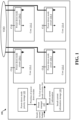
- FIG. 1 is a block diagram of an exemplary embodiment of a processor 100 configured to mange entering or exiting of power-down modes for multiple cores based on inrush current information.
- the processor 100 may be, for example, a processor for wireless communication.
- an exemplary apparatus may include the processor 100 or a cell phone incorporating the processor 100.
- the processor 100 may be a stand along processor or integrated in an end product, such as mobile phone, desktop computer, laptop computer, tablet computer, or the like.
- Each of the cores 110 may include a power-down mode circuit 104 (104-1, 104-2, 104-3, or 104-4 for each of the cores 110).
- the power-down mode circuits 104 may effect the corresponding cores 110 to enter or to exit various power-down modes.
- the power-down mode circuits 104 may cause the corresponding cores 110 to power up from a power-down mode, to power down to a power-down mode, or to transition among the various power-down modes.
- Examples of the power-down modes may include a power-collapse mode, in which all power is disconnected from the cores. Accordingly, the power-collapse mode may draw no current as all power is disconnected.
- Other power-down modes may include a clock-gating mode that disables clocking in the cores.
- Yet other power-down modes may include adjusting the operating voltages and frequencies of the cores. The entering and the exiting of the various power-down modes may take different amount of time. For example, entering and exiting the power-collapse mode may take more cycles than the other power-down modes.
- the power-down mode circuits 104 may effect the corresponding core 110 to enter into the power-collapse mode or the clock-gating mode (e.g., powering down the core 110).
- the power-down mode circuit 104 may likewise effect the core 110 to exit the power-down modes and return to full-power operations (e.g., powering up the core 110).
- the power-down mode circuit 104 may effect the corresponding core 110 to transition among the power-collapse mode and the clock-gating mode.
- the processor 100 further includes the power manager 105, the inrush current information storage 120, and the power-down mode priority storage 122.
- the power manager 105 may be configured to select among the cores 110 for entering or exiting power-down modes by selectively controlling the power-down mode circuits 104.
- the power manager 105 may include a processor (such as one of the cores 110) executing software instructions.
- the power manager 105 may select among the cores 110 based on inrush current information stored in the inrush current information storage 120 and/or the power-down mode priorities stored in the power-down mode priority storage 122.
- the stored inrush current information and/or the power-down mode priorities may be programmable (e.g., changed by software instructions).
- the power-down mode priority storage 122 may be, for example, registers storing power-down mode priorities.
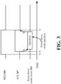
- the priorities may be, for example, based on the times to enter or to exit the power-down modes. For example, the power-collapse mode may take the longest to enter or to exit, and therefore, the power-collapse mode may have the lowest priority. In some examples, the priorities may be based on power saving of the power-down modes.
- the power manager control 205 may be further configured to select one or more of the cores 110 to grant to tokens so as not to cause the inrush current to spike exceeding an inrush current threshold (e.g., the inrush current budget). Additional features of this selection process are presented with FIGs. 4-5 .
- the process of requesting and granting the token is described below.
- the power manager 105 e.g., the power manager control 205 communicate with the cores 110 via the signaling REQ 206 (206-1 to 206-4 for each of the cores 110) and the signaling ACK 207 (207-1 to 207-4 for each of the cores 110).
- each of the cores 110 may independently and in parallel request a token from the power manager 105 by asserting the signaling REQ 206.
- the power-down mode circuit 104 causes the corresponding core 110 to power up to the full-power operation state, to power down to one of the power-down modes from the full-power operation state, or to transition among the power-down modes (at A).
- the requested power-down mode operation is completed.
- the power-down mode circuit 104 notifies the power manager 105 the release of the token by de-asserting (e.g., pulling low) both the signaling REQ 206 and the signaling ACK 207.
- the power manager control 205 receives token requests from the cores 110 (110-1 to 110-4) by receiving the low state of the signaling REQ 206-1 and the signaling REQ 206-2. The power manager control 205 then saves the requests in the token register 230 by storing "1"s in the bits 231 and 232, indicating respectively that the core 110-1 and 110-2 are requesting to enter or to exit at least one of the power-down modes.
- the selection of cores 110 allows for granting the maximum number of requests from the highest priority cores 110 (the cores 110 requesting to enter or to exit the power-down modes of highest priorities) within the inrush current budget. Such selection is made using the inrush current information of the highest priority cores 110.
- the remaining inrush current budget is utilized by selecting cores 110 of lower priorities (e.g., requesting to enter or exit power-down modes of lower priories) requiring inrush currents within the remaining inrush current budget. In such fashion, the core or cores 110 requesting to enter or to exit a first power-down mode and the core or cores 110 requesting to enter or to exit a second, different power-down mode may be selected concurrently.
- the power-down mode or modes requested by the selected one or more of the cores are entered or exited.
- the power-down mode circuits 104 of the selected cores 110 e.g., from operations 404 and 408 may cause the selected cores 110 to enter the requested power-down modes or to exit the current power-down mode.
- FIG. 5 is a block diagram of an exemplary embodiment of the power manager control 205.
- the block diagram may be an exemplary embodiment of a hardware implementation of the power manager control 205 and may include various (e.g., hardware and/or software) components. In some examples, theses components described below may include instructions executed by one of the cores 110-1 - 110-4.
- Software shall be construed broadly to mean instructions, instruction sets, code, code segments, program code, programs, subprograms, software modules, applications, software applications, software packages, routines, subroutines, objects, executables, threads of execution, procedures, functions, etc., whether referred to as software, firmware, middleware, microcode, hardware description language, or otherwise.
- the power manager control 205 includes the priority assignment component 502, the core selection component 504, and the request processing component 506.
- the priority assignment component 502 receives the requested power-down modes (to enter or to exit from) and the requesting cores 110 from the request processing component 506.
- the priority assignment component 502 further receives the power-down mode priorities from the programmable power-down mode priority storage 122.
- the priority assignment component 502 assigns priorities to the cores based on the power-down mode priorities (which are based on the time to enter or exit the power-down modes)(e.g., operation 403). In some examples, the priority assignment component 502 may increase the priorities of the unselected cores so as not to starve the unselected cores (e.g., operation 412).
- the core selection component 504 grants the maximum number of requests from the highest priority cores 110 (the cores 110 requesting to enter or to exit the power-down modes of highest priorities) within the inrush current budget. Such determination may be made using the inrush current information of the highest priority cores 110.
- the core selection component 504 may further utilizes the remaining inrush current budget by selecting cores 110 of lower priorities (e.g., requesting to enter or exit power-down modes of lower priories) requiring inrush currents within the remaining inrush current budget. In such fashion, the core selection component 504 may select concurrently the core or cores 110 requesting to enter or to exit a first power-down mode and the core or cores 110 requesting to enter or to exit a second, different power-down mode.
- the core selection component 504 is configured to select the one or more of the cores 110 to grant the power-down mode requests based on an the inrush current budget. Moreover, the number of the one or more of the cores 110 selected is based on the inrush current budget. See, for example, operation 408.
- the core selection component 504 receives notification of a completion of one of the selected cores 110 from the request processing component 506. In response, the core selection component 504 may perform the selections described above of the unselected cores 110 and new requesting cores 110. The unselected cores 110 may have increased priorities from the previous selection so as not to starve those cores 110.
Landscapes
- Engineering & Computer Science (AREA)
- Theoretical Computer Science (AREA)
- General Engineering & Computer Science (AREA)
- Physics & Mathematics (AREA)
- General Physics & Mathematics (AREA)
- Computer Hardware Design (AREA)
- Computing Systems (AREA)
- Power Sources (AREA)
- Direct Current Feeding And Distribution (AREA)
- Charge And Discharge Circuits For Batteries Or The Like (AREA)
Applications Claiming Priority (3)
| Application Number | Priority Date | Filing Date | Title |
|---|---|---|---|
| IN4955CH2015 | 2015-09-16 | ||
| US15/010,237 US9886081B2 (en) | 2015-09-16 | 2016-01-29 | Managing power-down modes |
| PCT/US2016/049504 WO2017048503A2 (en) | 2015-09-16 | 2016-08-30 | Managing power-down modes |
Publications (2)
| Publication Number | Publication Date |
|---|---|
| EP3350669A2 EP3350669A2 (en) | 2018-07-25 |
| EP3350669B1 true EP3350669B1 (en) | 2025-04-09 |
Family
ID=58258353
Family Applications (1)
| Application Number | Title | Priority Date | Filing Date |
|---|---|---|---|
| EP16767411.8A Active EP3350669B1 (en) | 2015-09-16 | 2016-08-30 | Managing power-down modes |
Country Status (6)
| Country | Link |
|---|---|
| US (1) | US9886081B2 (enExample) |
| EP (1) | EP3350669B1 (enExample) |
| JP (1) | JP6859327B2 (enExample) |
| KR (1) | KR102681069B1 (enExample) |
| CN (1) | CN108027636B (enExample) |
| WO (1) | WO2017048503A2 (enExample) |
Families Citing this family (9)
| Publication number | Priority date | Publication date | Assignee | Title |
|---|---|---|---|---|
| US9568982B1 (en) * | 2015-07-31 | 2017-02-14 | International Business Machines Corporation | Management of core power state transition in a microprocessor |
| US10025365B2 (en) * | 2016-06-23 | 2018-07-17 | Hewlett Packard Enterprise Development Lp | Power courses based on current changes |
| US10185378B2 (en) * | 2016-10-03 | 2019-01-22 | Microsoft Technology Licensing, Llc | Prioritized sequencing of device inrush current |
| JP2018136762A (ja) * | 2017-02-22 | 2018-08-30 | 富士通株式会社 | 並列処理装置および並列処理装置の起動方法 |
| US10423215B2 (en) * | 2017-05-15 | 2019-09-24 | Cavium, Llc | Methods and apparatus for adaptive power profiling in a baseband processing system |
| US10466766B2 (en) * | 2017-11-09 | 2019-11-05 | Qualcomm Incorporated | Grouping central processing unit memories based on dynamic clock and voltage scaling timing to improve dynamic/leakage power using array power multiplexers |
| US10948970B2 (en) * | 2018-03-30 | 2021-03-16 | Dialog Semiconductor B.V. | Low power microcontroller |
| US10528292B2 (en) * | 2018-05-22 | 2020-01-07 | Luca De Santis | Power down/power-loss memory controller |
| US20230367738A1 (en) * | 2022-05-11 | 2023-11-16 | Bae Systems Information And Electronic Systems Integration Inc. | Asic power control |
Family Cites Families (26)
| Publication number | Priority date | Publication date | Assignee | Title |
|---|---|---|---|---|
| JP3878431B2 (ja) | 2000-06-16 | 2007-02-07 | 株式会社ルネサステクノロジ | 半導体集積回路装置 |
| US7287170B2 (en) | 2002-05-14 | 2007-10-23 | Ati Technologies Inc. | Method and apparatus for power management using system and request tokens |
| US7065663B2 (en) | 2002-12-19 | 2006-06-20 | Intel Corporation | Methods and apparatus to control power state transitions |
| US7337334B2 (en) | 2003-02-14 | 2008-02-26 | International Business Machines Corporation | Network processor power management |
| US7380038B2 (en) | 2005-02-04 | 2008-05-27 | Microsoft Corporation | Priority registers for biasing access to shared resources |
| US7962771B2 (en) | 2007-12-31 | 2011-06-14 | Intel Corporation | Method, system, and apparatus for rerouting interrupts in a multi-core processor |
| US20100268917A1 (en) | 2009-04-17 | 2010-10-21 | Lsi Corporation | Systems and Methods for Ramped Power State Control in a Semiconductor Device |
| US9235251B2 (en) * | 2010-01-11 | 2016-01-12 | Qualcomm Incorporated | Dynamic low power mode implementation for computing devices |
| US9600059B2 (en) | 2010-09-20 | 2017-03-21 | Apple Inc. | Facilitating power management in a multi-core processor |
| US20130060555A1 (en) | 2011-06-10 | 2013-03-07 | Qualcomm Incorporated | System and Apparatus Modeling Processor Workloads Using Virtual Pulse Chains |
| US8601300B2 (en) * | 2011-09-21 | 2013-12-03 | Qualcomm Incorporated | System and method for managing thermal energy generation in a heterogeneous multi-core processor |
| US20130086395A1 (en) | 2011-09-30 | 2013-04-04 | Qualcomm Incorporated | Multi-Core Microprocessor Reliability Optimization |
| US8990604B2 (en) | 2011-10-14 | 2015-03-24 | Apple Inc. | Alternately sensing voltage on supply side or load side of a power gate of an electronic device and modifying feedback input of a power supply controlled by the power gate based on which side of the power gate is currently sensed |
| JP5786641B2 (ja) | 2011-10-25 | 2015-09-30 | 富士通株式会社 | 携帯端末装置の制御方法、制御プログラム及び携帯端末装置 |
| US9009451B2 (en) | 2011-10-31 | 2015-04-14 | Apple Inc. | Instruction type issue throttling upon reaching threshold by adjusting counter increment amount for issued cycle and decrement amount for not issued cycle |
| US9411407B2 (en) | 2012-12-12 | 2016-08-09 | Lenovo Enterprise Solutions (Singapore) Pte. Ltd. | Sequential power up of devices in a computing cluster based on relative commonality |
| CN104969142B (zh) | 2013-02-05 | 2017-09-19 | 高通股份有限公司 | 用于以有保证的瞬态最后期限来控制中央处理单元功率的系统和方法 |
| US9286223B2 (en) | 2013-04-17 | 2016-03-15 | Advanced Micro Devices, Inc. | Merging demand load requests with prefetch load requests |
| KR102063716B1 (ko) * | 2013-05-14 | 2020-02-11 | 삼성전자주식회사 | 데이터를 기반으로 전력을 관리하는 프로세싱 장치 및 그 장치를 이용한 방법 |
| US9007122B2 (en) * | 2013-06-05 | 2015-04-14 | Via Technologies, Inc. | Digital power gating with state retention |
| US9471088B2 (en) | 2013-06-25 | 2016-10-18 | Intel Corporation | Restricting clock signal delivery in a processor |
| US9495001B2 (en) * | 2013-08-21 | 2016-11-15 | Intel Corporation | Forcing core low power states in a processor |
| US20150149800A1 (en) | 2013-11-27 | 2015-05-28 | Alexander Gendler | Performing an operating frequency change using a dynamic clock control technique |
| US20150169363A1 (en) | 2013-12-18 | 2015-06-18 | Qualcomm Incorporated | Runtime Optimization of Multi-core System Designs for Increased Operating Life and Maximized Performance |
| US10114435B2 (en) * | 2013-12-23 | 2018-10-30 | Intel Corporation | Method and apparatus to control current transients in a processor |
| US9606605B2 (en) | 2014-03-07 | 2017-03-28 | Apple Inc. | Dynamic voltage margin recovery |
-
2016
- 2016-01-29 US US15/010,237 patent/US9886081B2/en active Active
- 2016-08-30 KR KR1020187010548A patent/KR102681069B1/ko active Active
- 2016-08-30 CN CN201680053355.4A patent/CN108027636B/zh active Active
- 2016-08-30 EP EP16767411.8A patent/EP3350669B1/en active Active
- 2016-08-30 JP JP2018513644A patent/JP6859327B2/ja active Active
- 2016-08-30 WO PCT/US2016/049504 patent/WO2017048503A2/en not_active Ceased
Also Published As
| Publication number | Publication date |
|---|---|
| JP6859327B2 (ja) | 2021-04-14 |
| EP3350669A2 (en) | 2018-07-25 |
| KR20180053732A (ko) | 2018-05-23 |
| CN108027636A (zh) | 2018-05-11 |
| US20170075408A1 (en) | 2017-03-16 |
| JP2018530824A (ja) | 2018-10-18 |
| WO2017048503A3 (en) | 2017-06-22 |
| KR102681069B1 (ko) | 2024-07-02 |
| US9886081B2 (en) | 2018-02-06 |
| CN108027636B (zh) | 2021-01-05 |
| WO2017048503A2 (en) | 2017-03-23 |
Similar Documents
| Publication | Publication Date | Title |
|---|---|---|
| EP3350669B1 (en) | Managing power-down modes | |
| US9703313B2 (en) | Peripheral clock management | |
| CN102692991B (zh) | 协调多个电路中的性能参数 | |
| US9128703B1 (en) | Processor that transitions to an idle mode when no task is scheduled to execute and further enters a quiescent doze mode or a wait mode depending on the value of a reference counter | |
| EP3198364B1 (en) | Novel low cost, low power high performance smp/asmp multiple-processor system | |
| US20140237276A1 (en) | Method and Apparatus for Determining Tunable Parameters to Use in Power and Performance Management | |
| US11762450B2 (en) | USB Type-C subsystem power management | |
| KR20130087583A (ko) | 컴퓨터 플랫폼의 시스템 전력 상태를 전환하는 방법, 장치 및 시스템 | |
| KR20120030763A (ko) | 계층적 전력 제어 회로, 이를 이용한 전력 제어 방법, 및 이를 포함하는 SoC 장치 | |
| US10147464B1 (en) | Managing power state in one power domain based on power states in another power domain | |
| BR112017007876B1 (pt) | Sistema de processamento de processador múltiplo, aparelho, método de comutação de uma pluralidade de processadores entre um modo de processamento múltiplo simétrico (smp) e um modo de processamento múltiplo assimétrico (asmp), e método de processamento em um sistema de processador múltiplo que tem uma pluralidade de processadores | |
| KR20220051159A (ko) | 디지털 방식으로 조정된 동적으로 적응가능한 클록 및 전압 공급 장치 및 방법 | |
| JP2023047293A (ja) | 決定論的省電力状態を達成するための装置及び方法 | |
| WO2016133613A1 (en) | Thermal mitigation with power duty cycle | |
| TWI470410B (zh) | 電子系統及其電源管理方法 | |
| US11705750B2 (en) | Power negotiation sequence to improve user experience and battery life | |
| US20140344596A1 (en) | Controlling Power Consumption Of A Processor Using Interrupt-Mediated On-Off Keying | |
| US9658682B2 (en) | Reference voltage circuits in microcontroller systems | |
| BR112018005212B1 (pt) | Gerenciamento de modos de desligamento | |
| KR20240165956A (ko) | 반도체 디바이스 동작 모드 관리 | |
| HK1172975A (en) | Coordinating performance parameters in multiple circuits |
Legal Events
| Date | Code | Title | Description |
|---|---|---|---|
| STAA | Information on the status of an ep patent application or granted ep patent |
Free format text: STATUS: THE INTERNATIONAL PUBLICATION HAS BEEN MADE |
|
| PUAI | Public reference made under article 153(3) epc to a published international application that has entered the european phase |
Free format text: ORIGINAL CODE: 0009012 |
|
| STAA | Information on the status of an ep patent application or granted ep patent |
Free format text: STATUS: REQUEST FOR EXAMINATION WAS MADE |
|
| 17P | Request for examination filed |
Effective date: 20180410 |
|
| AK | Designated contracting states |
Kind code of ref document: A2 Designated state(s): AL AT BE BG CH CY CZ DE DK EE ES FI FR GB GR HR HU IE IS IT LI LT LU LV MC MK MT NL NO PL PT RO RS SE SI SK SM TR |
|
| AX | Request for extension of the european patent |
Extension state: BA ME |
|
| DAV | Request for validation of the european patent (deleted) | ||
| DAX | Request for extension of the european patent (deleted) | ||
| STAA | Information on the status of an ep patent application or granted ep patent |
Free format text: STATUS: EXAMINATION IS IN PROGRESS |
|
| 17Q | First examination report despatched |
Effective date: 20191021 |
|
| GRAP | Despatch of communication of intention to grant a patent |
Free format text: ORIGINAL CODE: EPIDOSNIGR1 |
|
| STAA | Information on the status of an ep patent application or granted ep patent |
Free format text: STATUS: GRANT OF PATENT IS INTENDED |
|
| INTG | Intention to grant announced |
Effective date: 20241213 |
|
| GRAS | Grant fee paid |
Free format text: ORIGINAL CODE: EPIDOSNIGR3 |
|
| GRAA | (expected) grant |
Free format text: ORIGINAL CODE: 0009210 |
|
| STAA | Information on the status of an ep patent application or granted ep patent |
Free format text: STATUS: THE PATENT HAS BEEN GRANTED |
|
| AK | Designated contracting states |
Kind code of ref document: B1 Designated state(s): AL AT BE BG CH CY CZ DE DK EE ES FI FR GB GR HR HU IE IS IT LI LT LU LV MC MK MT NL NO PL PT RO RS SE SI SK SM TR |
|
| REG | Reference to a national code |
Ref country code: GB Ref legal event code: FG4D |
|
| REG | Reference to a national code |
Ref country code: CH Ref legal event code: EP |
|
| REG | Reference to a national code |
Ref country code: DE Ref legal event code: R096 Ref document number: 602016091843 Country of ref document: DE |
|
| REG | Reference to a national code |
Ref country code: IE Ref legal event code: FG4D |
|
| REG | Reference to a national code |
Ref country code: NL Ref legal event code: MP Effective date: 20250409 |
|
| PG25 | Lapsed in a contracting state [announced via postgrant information from national office to epo] |
Ref country code: NL Free format text: LAPSE BECAUSE OF FAILURE TO SUBMIT A TRANSLATION OF THE DESCRIPTION OR TO PAY THE FEE WITHIN THE PRESCRIBED TIME-LIMIT Effective date: 20250409 |
|
| REG | Reference to a national code |
Ref country code: AT Ref legal event code: MK05 Ref document number: 1784111 Country of ref document: AT Kind code of ref document: T Effective date: 20250409 |
|
| PG25 | Lapsed in a contracting state [announced via postgrant information from national office to epo] |
Ref country code: ES Free format text: LAPSE BECAUSE OF FAILURE TO SUBMIT A TRANSLATION OF THE DESCRIPTION OR TO PAY THE FEE WITHIN THE PRESCRIBED TIME-LIMIT Effective date: 20250409 Ref country code: FI Free format text: LAPSE BECAUSE OF FAILURE TO SUBMIT A TRANSLATION OF THE DESCRIPTION OR TO PAY THE FEE WITHIN THE PRESCRIBED TIME-LIMIT Effective date: 20250409 Ref country code: PT Free format text: LAPSE BECAUSE OF FAILURE TO SUBMIT A TRANSLATION OF THE DESCRIPTION OR TO PAY THE FEE WITHIN THE PRESCRIBED TIME-LIMIT Effective date: 20250811 |
|
| PGFP | Annual fee paid to national office [announced via postgrant information from national office to epo] |
Ref country code: DE Payment date: 20250709 Year of fee payment: 10 |
|
| REG | Reference to a national code |
Ref country code: LT Ref legal event code: MG9D |
|
| PG25 | Lapsed in a contracting state [announced via postgrant information from national office to epo] |
Ref country code: NO Free format text: LAPSE BECAUSE OF FAILURE TO SUBMIT A TRANSLATION OF THE DESCRIPTION OR TO PAY THE FEE WITHIN THE PRESCRIBED TIME-LIMIT Effective date: 20250709 Ref country code: GR Free format text: LAPSE BECAUSE OF FAILURE TO SUBMIT A TRANSLATION OF THE DESCRIPTION OR TO PAY THE FEE WITHIN THE PRESCRIBED TIME-LIMIT Effective date: 20250710 |
|
| PG25 | Lapsed in a contracting state [announced via postgrant information from national office to epo] |
Ref country code: PL Free format text: LAPSE BECAUSE OF FAILURE TO SUBMIT A TRANSLATION OF THE DESCRIPTION OR TO PAY THE FEE WITHIN THE PRESCRIBED TIME-LIMIT Effective date: 20250409 |
|
| PG25 | Lapsed in a contracting state [announced via postgrant information from national office to epo] |
Ref country code: BG Free format text: LAPSE BECAUSE OF FAILURE TO SUBMIT A TRANSLATION OF THE DESCRIPTION OR TO PAY THE FEE WITHIN THE PRESCRIBED TIME-LIMIT Effective date: 20250409 |
|
| PGFP | Annual fee paid to national office [announced via postgrant information from national office to epo] |
Ref country code: GB Payment date: 20250710 Year of fee payment: 10 |
|
| PG25 | Lapsed in a contracting state [announced via postgrant information from national office to epo] |
Ref country code: HR Free format text: LAPSE BECAUSE OF FAILURE TO SUBMIT A TRANSLATION OF THE DESCRIPTION OR TO PAY THE FEE WITHIN THE PRESCRIBED TIME-LIMIT Effective date: 20250409 |
|
| PG25 | Lapsed in a contracting state [announced via postgrant information from national office to epo] |
Ref country code: AT Free format text: LAPSE BECAUSE OF FAILURE TO SUBMIT A TRANSLATION OF THE DESCRIPTION OR TO PAY THE FEE WITHIN THE PRESCRIBED TIME-LIMIT Effective date: 20250409 |
|
| PGFP | Annual fee paid to national office [announced via postgrant information from national office to epo] |
Ref country code: FR Payment date: 20250709 Year of fee payment: 10 |
|
| PG25 | Lapsed in a contracting state [announced via postgrant information from national office to epo] |
Ref country code: RS Free format text: LAPSE BECAUSE OF FAILURE TO SUBMIT A TRANSLATION OF THE DESCRIPTION OR TO PAY THE FEE WITHIN THE PRESCRIBED TIME-LIMIT Effective date: 20250709 |
|
| PG25 | Lapsed in a contracting state [announced via postgrant information from national office to epo] |
Ref country code: IS Free format text: LAPSE BECAUSE OF FAILURE TO SUBMIT A TRANSLATION OF THE DESCRIPTION OR TO PAY THE FEE WITHIN THE PRESCRIBED TIME-LIMIT Effective date: 20250809 |
|
| PG25 | Lapsed in a contracting state [announced via postgrant information from national office to epo] |
Ref country code: LV Free format text: LAPSE BECAUSE OF FAILURE TO SUBMIT A TRANSLATION OF THE DESCRIPTION OR TO PAY THE FEE WITHIN THE PRESCRIBED TIME-LIMIT Effective date: 20250409 |