EP3349348A1 - Elektrische schaltungsvorrichtung - Google Patents
Elektrische schaltungsvorrichtung Download PDFInfo
- Publication number
- EP3349348A1 EP3349348A1 EP16844083.2A EP16844083A EP3349348A1 EP 3349348 A1 EP3349348 A1 EP 3349348A1 EP 16844083 A EP16844083 A EP 16844083A EP 3349348 A1 EP3349348 A1 EP 3349348A1
- Authority
- EP
- European Patent Office
- Prior art keywords
- connector
- case
- substrate
- opening
- opening portion
- Prior art date
- Legal status (The legal status is an assumption and is not a legal conclusion. Google has not performed a legal analysis and makes no representation as to the accuracy of the status listed.)
- Withdrawn
Links
Images







Classifications
-
- H—ELECTRICITY
- H02—GENERATION; CONVERSION OR DISTRIBUTION OF ELECTRIC POWER
- H02G—INSTALLATION OF ELECTRIC CABLES OR LINES, OR OF COMBINED OPTICAL AND ELECTRIC CABLES OR LINES
- H02G3/00—Installations of electric cables or lines or protective tubing therefor in or on buildings, equivalent structures or vehicles
- H02G3/02—Details
- H02G3/08—Distribution boxes; Connection or junction boxes
- H02G3/16—Distribution boxes; Connection or junction boxes structurally associated with support for line-connecting terminals within the box
-
- H—ELECTRICITY
- H01—ELECTRIC ELEMENTS
- H01R—ELECTRICALLY-CONDUCTIVE CONNECTIONS; STRUCTURAL ASSOCIATIONS OF A PLURALITY OF MUTUALLY-INSULATED ELECTRICAL CONNECTING ELEMENTS; COUPLING DEVICES; CURRENT COLLECTORS
- H01R13/00—Details of coupling devices of the kinds covered by groups H01R12/70 or H01R24/00 - H01R33/00
- H01R13/46—Bases; Cases
- H01R13/502—Bases; Cases composed of different pieces
-
- H—ELECTRICITY
- H01—ELECTRIC ELEMENTS
- H01R—ELECTRICALLY-CONDUCTIVE CONNECTIONS; STRUCTURAL ASSOCIATIONS OF A PLURALITY OF MUTUALLY-INSULATED ELECTRICAL CONNECTING ELEMENTS; COUPLING DEVICES; CURRENT COLLECTORS
- H01R13/00—Details of coupling devices of the kinds covered by groups H01R12/70 or H01R24/00 - H01R33/00
- H01R13/46—Bases; Cases
- H01R13/52—Dustproof, splashproof, drip-proof, waterproof, or flameproof cases
- H01R13/5202—Sealing means between parts of housing or between housing part and a wall, e.g. sealing rings
-
- H—ELECTRICITY
- H01—ELECTRIC ELEMENTS
- H01R—ELECTRICALLY-CONDUCTIVE CONNECTIONS; STRUCTURAL ASSOCIATIONS OF A PLURALITY OF MUTUALLY-INSULATED ELECTRICAL CONNECTING ELEMENTS; COUPLING DEVICES; CURRENT COLLECTORS
- H01R13/00—Details of coupling devices of the kinds covered by groups H01R12/70 or H01R24/00 - H01R33/00
- H01R13/46—Bases; Cases
- H01R13/52—Dustproof, splashproof, drip-proof, waterproof, or flameproof cases
- H01R13/5219—Sealing means between coupling parts, e.g. interfacial seal
-
- H—ELECTRICITY
- H01—ELECTRIC ELEMENTS
- H01R—ELECTRICALLY-CONDUCTIVE CONNECTIONS; STRUCTURAL ASSOCIATIONS OF A PLURALITY OF MUTUALLY-INSULATED ELECTRICAL CONNECTING ELEMENTS; COUPLING DEVICES; CURRENT COLLECTORS
- H01R13/00—Details of coupling devices of the kinds covered by groups H01R12/70 or H01R24/00 - H01R33/00
- H01R13/62—Means for facilitating engagement or disengagement of coupling parts or for holding them in engagement
- H01R13/629—Additional means for facilitating engagement or disengagement of coupling parts, e.g. aligning or guiding means, levers, gas pressure electrical locking indicators, manufacturing tolerances
- H01R13/631—Additional means for facilitating engagement or disengagement of coupling parts, e.g. aligning or guiding means, levers, gas pressure electrical locking indicators, manufacturing tolerances for engagement only
- H01R13/6315—Additional means for facilitating engagement or disengagement of coupling parts, e.g. aligning or guiding means, levers, gas pressure electrical locking indicators, manufacturing tolerances for engagement only allowing relative movement between coupling parts, e.g. floating connection
-
- H—ELECTRICITY
- H01—ELECTRIC ELEMENTS
- H01R—ELECTRICALLY-CONDUCTIVE CONNECTIONS; STRUCTURAL ASSOCIATIONS OF A PLURALITY OF MUTUALLY-INSULATED ELECTRICAL CONNECTING ELEMENTS; COUPLING DEVICES; CURRENT COLLECTORS
- H01R13/00—Details of coupling devices of the kinds covered by groups H01R12/70 or H01R24/00 - H01R33/00
- H01R13/73—Means for mounting coupling parts to apparatus or structures, e.g. to a wall
- H01R13/74—Means for mounting coupling parts in openings of a panel
- H01R13/748—Means for mounting coupling parts in openings of a panel using one or more screws
-
- H—ELECTRICITY
- H02—GENERATION; CONVERSION OR DISTRIBUTION OF ELECTRIC POWER
- H02G—INSTALLATION OF ELECTRIC CABLES OR LINES, OR OF COMBINED OPTICAL AND ELECTRIC CABLES OR LINES
- H02G3/00—Installations of electric cables or lines or protective tubing therefor in or on buildings, equivalent structures or vehicles
- H02G3/02—Details
- H02G3/08—Distribution boxes; Connection or junction boxes
- H02G3/088—Dustproof, splashproof, drip-proof, waterproof, or flameproof casings or inlets
-
- H—ELECTRICITY
- H02—GENERATION; CONVERSION OR DISTRIBUTION OF ELECTRIC POWER
- H02M—APPARATUS FOR CONVERSION BETWEEN AC AND AC, BETWEEN AC AND DC, OR BETWEEN DC AND DC, AND FOR USE WITH MAINS OR SIMILAR POWER SUPPLY SYSTEMS; CONVERSION OF DC OR AC INPUT POWER INTO SURGE OUTPUT POWER; CONTROL OR REGULATION THEREOF
- H02M7/00—Conversion of AC power input into DC power output; Conversion of DC power input into AC power output
- H02M7/003—Constructional details, e.g. physical layout, assembly, wiring or busbar connections
-
- H—ELECTRICITY
- H02—GENERATION; CONVERSION OR DISTRIBUTION OF ELECTRIC POWER
- H02M—APPARATUS FOR CONVERSION BETWEEN AC AND AC, BETWEEN AC AND DC, OR BETWEEN DC AND DC, AND FOR USE WITH MAINS OR SIMILAR POWER SUPPLY SYSTEMS; CONVERSION OF DC OR AC INPUT POWER INTO SURGE OUTPUT POWER; CONTROL OR REGULATION THEREOF
- H02M7/00—Conversion of AC power input into DC power output; Conversion of DC power input into AC power output
- H02M7/42—Conversion of DC power input into AC power output without possibility of reversal
- H02M7/44—Conversion of DC power input into AC power output without possibility of reversal by static converters
- H02M7/48—Conversion of DC power input into AC power output without possibility of reversal by static converters using discharge tubes with control electrode or semiconductor devices with control electrode
-
- H—ELECTRICITY
- H05—ELECTRIC TECHNIQUES NOT OTHERWISE PROVIDED FOR
- H05K—PRINTED CIRCUITS; CASINGS OR CONSTRUCTIONAL DETAILS OF ELECTRIC APPARATUS; MANUFACTURE OF ASSEMBLAGES OF ELECTRICAL COMPONENTS
- H05K5/00—Casings, cabinets or drawers for electric apparatus
- H05K5/06—Hermetically-sealed casings
- H05K5/069—Other details of the casing, e.g. wall structure, passage for a connector, a cable, a shaft
-
- H—ELECTRICITY
- H05—ELECTRIC TECHNIQUES NOT OTHERWISE PROVIDED FOR
- H05K—PRINTED CIRCUITS; CASINGS OR CONSTRUCTIONAL DETAILS OF ELECTRIC APPARATUS; MANUFACTURE OF ASSEMBLAGES OF ELECTRICAL COMPONENTS
- H05K7/00—Constructional details common to different types of electric apparatus
- H05K7/14—Mounting supporting structure in casing or on frame or rack
- H05K7/1422—Printed circuit boards receptacles, e.g. stacked structures, electronic circuit modules or box like frames
- H05K7/1427—Housings
- H05K7/1432—Housings specially adapted for power drive units or power converters
- H05K7/14322—Housings specially adapted for power drive units or power converters wherein the control and power circuits of a power converter are arranged within the same casing
-
- H—ELECTRICITY
- H01—ELECTRIC ELEMENTS
- H01R—ELECTRICALLY-CONDUCTIVE CONNECTIONS; STRUCTURAL ASSOCIATIONS OF A PLURALITY OF MUTUALLY-INSULATED ELECTRICAL CONNECTING ELEMENTS; COUPLING DEVICES; CURRENT COLLECTORS
- H01R12/00—Structural associations of a plurality of mutually-insulated electrical connecting elements, specially adapted for printed circuits, e.g. printed circuit boards [PCB], flat or ribbon cables, or like generally planar structures, e.g. terminal strips, terminal blocks; Coupling devices specially adapted for printed circuits, flat or ribbon cables, or like generally planar structures; Terminals specially adapted for contact with, or insertion into, printed circuits, flat or ribbon cables, or like generally planar structures
- H01R12/70—Coupling devices
- H01R12/71—Coupling devices for rigid printing circuits or like structures
- H01R12/712—Coupling devices for rigid printing circuits or like structures co-operating with the surface of the printed circuit or with a coupling device exclusively provided on the surface of the printed circuit
- H01R12/716—Coupling device provided on the PCB
-
- H—ELECTRICITY
- H01—ELECTRIC ELEMENTS
- H01R—ELECTRICALLY-CONDUCTIVE CONNECTIONS; STRUCTURAL ASSOCIATIONS OF A PLURALITY OF MUTUALLY-INSULATED ELECTRICAL CONNECTING ELEMENTS; COUPLING DEVICES; CURRENT COLLECTORS
- H01R2201/00—Connectors or connections adapted for particular applications
- H01R2201/26—Connectors or connections adapted for particular applications for vehicles
Definitions
- the present invention relates to an electric circuit apparatus.
- An electric circuit apparatus includes: a connector that transmits one of a driving current and a signal to an electric circuit unit; a substrate connected to the connector; a first case member forming an housing space for the substrate and forming an opening portion; and an intermediate member interposed between the connector and the first case member, in which the intermediate member includes a connector-side opening portion through which the connector passes, a seal surface with the connector, and a fixing portion to be fixed on the first case member, and the fixing portion is formed so as to absorb a positional tolerance between the connector and the opening portion of the first case member.
- FIG. 1 is a perspective view illustrating an appearance of a power conversion apparatus according to the present embodiment.
- FIG. 2 is an exploded view of the power conversion apparatus.
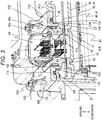
- FIG. 3 is a perspective view of a cross section taken along plane A-A in FIG. 1 .
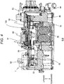
- FIG. 4 is a cross-sectional view taken along plane D-D of FIG. 1 .
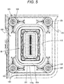
- FIG. 5 is a top view of the vicinity of a signal connector.
- an up-down direction (upward/downward) of the power conversion apparatus is defined as illustrated in FIGS. 1 to 4 .
- a power conversion apparatus 1 converts a DC current supplied from a battery as a DC current power supply into an AC current and supplies the AC current to the rotating electric machine. Also, during regenerative operation, the rotating electric machine operates as a generator, and the power conversion apparatus 1 charges the battery by converting the AC current from the rotating electric machine into the DC current.
- the power conversion apparatus 1 includes a power module 10, a capacitor module 20, a driver circuit substrate 30 (refer to FIGS. 3 and 4 ), a control circuit substrate 40, a substrate support member 50, and a first case 60 and a second case 70 constituting a housing storing these components.
- the power module 10 includes a plurality of switching power semiconductors constituting an inverter circuit.
- an insulated gate bipolar transistor is used as the switching power semiconductor, which will be hereinafter abbreviated as an IGBT.
- a metal oxide semiconductor field effect transistor may be used as the switching power semiconductor.
- the control circuit substrate 40 includes a control circuit 41.
- the control circuit 41 includes a microcomputer that performs arithmetic processing of the switching timing of each of the IGBT.
- a target torque value demanded for a rotating electric machine (not illustrated) is input into the control circuit 41 from a host controller (not illustrated) via a signal connector 80 described below.
- the control circuit 41 On the basis of the target torque value input from the host controller, current information from a current sensor (not illustrated), and a magnetic pole position of a rotor of the rotating electric machine, the control circuit 41 generates a control pulse as a control signal for controlling each of the IGBT and inputs the pulse into a driver circuit 31 described below.
- the magnetic pole position is detected on the basis of a detection signal output from a rotating magnetic pole sensor such as a resolver provided in the rotating electric machine.
- the driver circuit substrate 30 includes the driver circuit 31.
- the driver circuit 31 supplies a drive pulse for controlling each of the IGBT to each of the IGBT via wires for gate drive signals.
- Each of the IGBT performs conduction or blocking operation on the basis of the drive pulse from the driver circuit 31 and converts the DC current into a three-phase AC current.
- the first case 60 is a member having a lidded and bottomless box shape, and includes an opening portion 61 on its upper surface ( FIGS. 2 and 3 ).
- the signal connector 80 protrudes from an opening 61a of the opening portion 61 ( FIGS. 1 and 3 ).
- a plane including an opening surface of the opening portion 61 is indicated by a broken line. This plane is referred to as an opening plane 61b.
- the opening plane 61b extends in a direction orthogonal to the up-down direction.
- a female screw 63 is engraved on the case-side boss 62. As illustrated in FIGS.
- an intermediate member 100 is attached on a portion of the upper surface of the first case 60 so as to cover the opening portion 61 using the four case-side bosses 62 as described in detail below.
- the intermediate member 100 includes an opening at the center, and the signal connector 80 passes through this central opening. Details of the signal connector 80 and the intermediate member 100 will be described below.
- the first case 60 forms a housing space to house the driver circuit substrate 30, the control circuit substrate 40, and the substrate support member 50.
- the second case 70 is attached to a lower portion of the first case 60.
- the second case 70 is a member having a bottomed uncovered box shape that houses a portion of the power module 10 and a portion of the capacitor module 20.
- the second case 70 includes a fixing portion (not illustrated) that fixes the power module 10, a fixing portion (not illustrated) that fixes the capacitor module 20, and a fixing portion 73 that fixes the substrate support member 50.
- the fixing portion 73 protrudes more upward than an upper end of a peripheral wall of the second case 70.
- the substrate support member 50 is a plate-like member to which the control circuit substrate 40 is attached on the upper surface and the driver circuit substrate 30 is attached to the lower surface.
- the substrate support member 50 is fixed to the fixing portion 73 of the second case 70.
- a substrate contact portion 51 protrudes at a position facing the connector-side substrate contact portion 84 of the signal connector 80 described below.
- the pressing force buffering material 52 is a soft plate-like member formed of rubber, for example, and is interposed between the substrate support member 50 and the control circuit substrate 40.
- the signal connector 80 illustrated in FIGS. 6 to 9 is attached on the upper surface of the control circuit substrate 40.
- FIG. 6 is a plan view of the signal connector 80
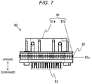
- FIGS. 7 and 8 are side views of the signal connector 80
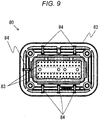
- FIG. 9 is a bottom view of the signal connector 80.
- the signal connector 80 is a connector to be connected to a host controller (not illustrated) as described above, and includes a connector main body 81, a seal member 82, a signal pin 83, and a connector-side substrate contact portion 84.
- the connector main body 81 is a member that holds the signal pin 83, and is constituted with two members, an upper main body 81a and a lower main body 81b in the present embodiment.
- the upper main body 81a has a substantially rectangular shape in plan view and is fitted and connected to an external connection member 89 illustrated in FIG. 1 .
- the lower main body 81b includes a groove 81c along the entire circumference of its outer periphery.
- a ring-shaped seal member 82 is fitted in the groove 81c.
- the signal pin 83 is held by the connector main body 81, with its lower end being connected and fixed to the control circuit substrate 40 by solder or the like. In this manner, the signal connector 80 is fixed to the control circuit substrate 40.
- the connector-side substrate contact portion 84 is a portion that abuts the upper surface of the circuit substrate 40, and is formed on the lower surface of the connector main body 81.
- the connector-side substrate contact portion 84 is provided at a position facing the substrate contact portion 51 of the substrate support member 50.
- the connector-side substrate contact portion 84 transmits a downward force acting on the signal connector 80 to the substrate contact portion 51 of the substrate support member 50 via the circuit substrate 40 and the pressing force buffering material 52.
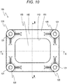
- FIG. 10 is a plan view of the intermediate member 100.
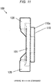
- FIGS. 11 and 12 are side views of the intermediate member 100.
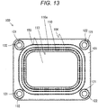
- FIG. 13 is a bottom view of the intermediate member 100.
- FIG. 14 is a cross-sectional view taken along arrow B-B in FIG. 9 .
- FIG. 15 is a cross sectional view taken along arrow C-C in FIG. 10 .
- the intermediate member 100 is a member that closes a gap between the opening portion 61 of the first case 60 and the signal connector 80.
- the intermediate member 100 includes an intermediate member main body 101.
- the intermediate member main body 101 is a plate-like member having a substantially rectangular shape in plan view, and includes a connector-side opening forming portion 102, an insertion portion 110, and a fixing portion 120.
- the connector-side opening forming portion 102 includes an opening 103 of a substantially rectangular shape formed on the intermediate member main body 101 at the center in plan view.
- the opening 103 is an opening through which the signal connector 80 passes.
- the insertion portion 110 is protruded from the lower surface of the connector-side opening forming portion 102.
- the insertion portion 110 is a rectangular ring-shaped portion protruding downward from the intermediate member main body 101.
- An outer peripheral portion of the insertion portion 110 is referred to as an outer peripheral portion 110a.
- the insertion portion 110 is inserted through the opening 61a of the opening portion 61 of the first case 60. That is, the diameter of the outer peripheral portion 110a of the insertion portion 110 is smaller than the diameter of the opening 61a of the opening portion 61 of the first case 60 by a predetermined gap. This gap will be described in detail below.
- the insertion portion 110 includes: an upper inner peripheral portion connected to the connector-side opening forming portion 102 and having a same inner diameter as the inner periphery of the connector-side opening forming portion 102; and a tapered portion 111 having an increased inner diameter more toward a lower side from the upper inner peripheral portion.
- the connector-side opening forming portion 102 and the upper inner peripheral portion of the insertion portion 110 constitute a first seal portion 113 that seals between the signal connector 80 and the first case 60, together with the seal member 82 of the signal connector 80, as will be described below.
- the inner peripheral surface of the first seal portion 113 forms a first seal surface 112 that abuts the seal member 82.
- first seal portion 113 is formed in the connector-side opening forming portion 102 and the upper inner peripheral portion of the insertion portion 110 in this manner, it is possible to ensure a sufficiently large distance of the first seal surface 112 of the first seal portion 113 in the up-down direction.
- the fixing portion 120 is provided at four corners of the intermediate member main body 101 in plan view. Together with the case-side boss 62, the fixing portion 120 fixes the intermediate member 100 to the first case 60. As is apparent from FIGS. 10 and 16 , the fixing portion 120 has a cylindrical shape having a stepped hole. Note that FIG. 16 is a cross-sectional view taken along plane E-E in FIG. 1 , and illustrates a vertical cross section of the fixing portion 120. The inner diameter of the stepped hole of the fixing portion 120 is larger in a lower hole 122 than in an upper hole 121.
- the inner diameter of the upper hole 121 is smaller than the outer diameter of the case-side boss 62 of the first case 60, while the inner diameter of the lower hole 122 is larger than the outer diameter of the case-side boss 62.
- the inner peripheral surface of the hole 122 faces the outer peripheral surface of the case-side boss 62. Therefore, the hole 122 is also referred to as a boss facing portion.
- a seal groove 104 is provided on a lower surface of the intermediate member main body 101.
- the seal groove 104 is provided outside the outer peripheral portion 110a of the insertion portion 110 in plan view.
- a seal member 105 illustrated in FIG. 2 is inserted into the seal groove 104.
- a portion where the seal groove 104 is formed is referred to as a second seal portion 114.
- the power module 10 and the capacitor module 20 are individually housed in and fixed to the second case 70. With this operation, the power module 10 and the capacitor module 20 are arranged side by side.
- the driver circuit substrate 30 is attached on the lower surface the substrate support member 50 and the control circuit substrate 40 is attached to the upper surface thereof, in advance. Subsequently, the substrate support member 50 is fixed to the fixing portion 73 of the second case 70. With this operation, the driver circuit substrate 30 and the control circuit substrate 40 are fixed to the second case 70 via the substrate support member 50.
- the driver circuit substrate 30, the control circuit substrate 40, and the substrate support member 50 are arranged above the power module 10 and the capacitor module 20.
- the signal connector 80 is attached to the control circuit substrate 40 in advance.
- the pressing force buffering material 52 is arranged between the substrate contact portion 51 of the substrate support member 50 and the lower surface of the control circuit substrate 40.
- the control circuit substrate 40 may be attached to the substrate support member 50 after fixing the substrate support member 50 to the fixing portion 73 of the second case 70.
- the first case 60 is attached to the second case 70. That is, the second case 70 and the first case 60 are arranged to face each other, and the individual peripheral wall portions are fastened with bolts.
- the signal connector 80 protrudes from the opening 61a of the opening portion 61 of the first case 60. In this state, a gap is formed between the opening portion 61 and the outer periphery of the signal connector 80.
- the intermediate member 100 is guided by the outer periphery of the connector main body 81 of the signal connector 80 and by the tapered portion 111 of the insertion portion 110 of the intermediate member 100. Subsequently, the connector main body 81 of the signal connector 80 is inserted into the opening 103 of the intermediate member main body 101.
- the intermediate member 100 moves parallel to the opening plane 61b in accordance with the signal connector 80 by the action of the tapered portion 111 of the insertion portion 110, determining the position in plan view.
- the first seal surface 112 abuts the outer periphery of the seal member 82 of the signal connector 80 and pressurizes the seal member 82. With this operation, a gap between the first seal surface 112 and the outer periphery of the connector main body 81 is sealed.
- the insertion portion 110 is inserted into the opening 61a of the opening portion 61.
- the case-side boss 62 of the first case 60 enters the lower hole 122 of the fixing portion 120 of the intermediate member 100. Subsequently, a lower surface of the step portion of the upper hole 121 and the lower hole 122 of the fixing portion 120 abuts an upper end of the case-side boss 62 (refer to FIG. 16 ). Moreover, the lower surface of the seal member 105 abuts the upper surface of the opening portion 61 and is pressurized. With this operation, the space between the lower surface of the intermediate member main body 101 and the upper surface of the opening portion 61 is sealed (refer to FIG. 3 ). When the intermediate member 100 is attached, the signal connector 80 protrudes from the opening 103 (refer to FIGS. 1 and 3 ).
- the fixing portion 120 is fixed to the case-side boss 62 with a bolt 123, on the intermediate member 100.
- the bolt 123 pressurizes the upper surface of the fixing portion 120 downward via the washer, presses the fixing portion 120 against the upper end of the case-side boss 62, thereby fixing the intermediate member 100 to the first case 60. In this manner, the power conversion apparatus 1 is assembled.
- the control circuit substrate 40 and the substrate support member 50 are positioned by a first positioning portion 91 surrounded by a broken line, while the first case 60 and the substrate support member 50 are positioned by a second positioning portion 92 surrounded by a broken line.
- the substrate support member 50 and the second case 70 are positioned by a third positioning portion 93 surrounded by a broken line, while the first case 60 and the second case 70 are positioned by a fourth positioning portion 94 surrounded by a broken line There.
- a positioning pin is inserted through a positioning hole provided in the control circuit substrate 40 and the substrate support member 50.
- a positioning pin is inserted through a positioning hole provided in the first case 60 and the substrate support member 50.
- a positioning pin is inserted through a positioning hole provided in the substrate support member 50 and the second case 70.
- a positioning pin is inserted through a positioning hole provided in the first case 60 and the second case 70.
- the power conversion apparatus 1 configured in this manner is mounted on an electric vehicle.
- the signal connector 80 is connected to the external connection member 89 (refer to FIG. 1 ) in order to connect the host controller (not illustrated) and the control circuit 41.
- a downward pressurizing force acts on the signal connector 80 from the external connection member 89.
- the pressing force buffering material 52 absorbs the pressurizing force acting on the signal connector 80, and the substrate contact portion 51 distributes the pressurizing force acting on the signal connector 80 to the substrate support member 50 and the second case 70.
- the signal connector 80 when attaching the intermediate member 100, the signal connector 80 receives a downward pressurizing force from the intermediate member 100 due to the friction between the first seal surface 112 of the intermediate member 100 and the seal member 82 of the signal connector 80.
- the pressing force buffering material 52 absorbs the pressurizing force acting on the signal connector 80, and the substrate contact portion 51 distributes the pressurizing force acting on the signal connector 80 to the substrate support member 50 and the second case 70. This configuration makes it possible to prevent damage to the connection portion due to solder or the like between the signal pin 83 and the control circuit substrate 40 attributed to the pressurizing force acting on the signal connector 80.
- the control circuit substrate 40 to which the signal connector 80 has been attached is fixed to the second case 70 via the substrate support member 50. Moreover, the first case 60 is fixed to the second case 70 to which the control circuit substrate 40 has been fixed.
- This generates variation in a positional relationship between the signal connector 80 and the opening 61a of the opening portion 61 in plan view.
- the variation in the positional relationship between the signal connector 80 and the opening 61a of the opening portion 61 in plan view will be referred to as a positional tolerance between the signal connector 80 and the opening 61a of the opening portion 61, or simply a positional tolerance. In the following, this positional tolerance will be described in two manners.
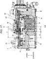
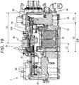
- the dimension L6 would be equal to the dimension obtained by subtracting the dimension L2 from the sum of the dimension L4 and the dimension L5. That is, the following formula (4) would be established.
- L 6 ⁇ L 4 + L 5 ⁇ L 2 0
- C is a sum of dimensional tolerances of the dimensions L2, L4 to L6, and is a positive or negative value.
- the control circuit substrate 40 and the substrate support member 50 in the first positioning portion 91 there is play between the control circuit substrate 40 and the substrate support member 50 in the first positioning portion 91, and there is play between the substrate support member 50 and the second case 70 in the third positioning portion 93, and there is play between the first case 60 and the second case 70 in the fourth positioning portion 94.
- the sum of the play between the control circuit substrate 40 and the substrate support member 50 in the first positioning portion 91, the play between the substrate support member 50 and the second case 70 in the third positioning portion 93, and the play between the first case 60 and the second case 70 in the fourth positioning portion 94 is represented by D.
- the sum D of the play is a positive or negative value.
- the positional tolerance between the signal connector 80 and the opening 61a of the opening portion 61 is the sum of the value C represented by the above-described formula (5) and the above-described sum D of the plays, and is expressed by the following formula (6).
- Positional tolerance C + D
- the position of the intermediate member 100 in plan view is determined in accordance with the signal connector 80, the positional tolerance between the outer peripheral portion 110a of the insertion portion 110 of the intermediate member 100 and the opening 61a of the opening portion 61 is substantially equal to the above-described positional tolerance between the connector 80 and the opening 61a of the opening portion 61. Therefore, it is preferable that the size of the opening 61a of the opening portion 61 be larger than the size of the outer peripheral portion 110a of the insertion portion 110 by at least the above-described positional tolerance. As illustrated in FIGS. 3 and 5 , in the power conversion apparatus 1 according to the present embodiment, there is provided a gap 131 that absorbs the above-described positional tolerance between the opening 61a of the opening portion 61 and the outer peripheral portion 110a of the insertion portion 110.
- the inner diameter of the lower hole 122 of the fixing portion 120 be larger than the outer diameter of the case-side boss 62 by at least the above-described positional tolerance.
- the inner diameter of the upper hole 121 of the fixing portion 120 be larger than the diameter of the bolt 123 by at least the above-described positional tolerance.
- a gap 132 that absorbs the above-described positional tolerance between the inner peripheral surface of the lower hole 122 of the fixing portion 120 and the outer peripheral surface of the case-side boss 62, and there is provided a gap 133 that absorbs the above-described positional tolerance between the inner peripheral surface of the upper hole 121 of the fixing portion 120 and the bolt 123.
- the above-described power conversion apparatus 1 achieves the following operational effects.
- the present invention is not limited to the above-described embodiments, and other forms conceivable within the technical scope of the present invention are also included in the scope of the present invention as long as the features of the present invention can be maintained. Furthermore, a combination of the above-described embodiment(s) and a plurality of modifications may be adopted.
Landscapes
- Engineering & Computer Science (AREA)
- Power Engineering (AREA)
- Architecture (AREA)
- Civil Engineering (AREA)
- Structural Engineering (AREA)
- Microelectronics & Electronic Packaging (AREA)
- Inverter Devices (AREA)
- Mounting Of Printed Circuit Boards And The Like (AREA)
Applications Claiming Priority (2)
| Application Number | Priority Date | Filing Date | Title |
|---|---|---|---|
| JP2015179051 | 2015-09-11 | ||
| PCT/JP2016/072575 WO2017043219A1 (ja) | 2015-09-11 | 2016-08-02 | 電気回路装置 |
Publications (2)
| Publication Number | Publication Date |
|---|---|
| EP3349348A1 true EP3349348A1 (de) | 2018-07-18 |
| EP3349348A4 EP3349348A4 (de) | 2019-03-27 |
Family
ID=58239411
Family Applications (1)
| Application Number | Title | Priority Date | Filing Date |
|---|---|---|---|
| EP16844083.2A Withdrawn EP3349348A4 (de) | 2015-09-11 | 2016-08-02 | Elektrische schaltungsvorrichtung |
Country Status (5)
| Country | Link |
|---|---|
| US (1) | US10277019B2 (de) |
| EP (1) | EP3349348A4 (de) |
| JP (1) | JP6797123B2 (de) |
| CN (1) | CN108028611B (de) |
| WO (1) | WO2017043219A1 (de) |
Families Citing this family (12)
| Publication number | Priority date | Publication date | Assignee | Title |
|---|---|---|---|---|
| US11284529B2 (en) * | 2016-12-14 | 2022-03-22 | Lg Innotek Co., Ltd. | Electronic component housing and DC-DC converter comprising same |
| CN108281835B (zh) * | 2017-01-06 | 2024-04-09 | 西霸士电子(厦门)有限公司 | 锁紧装置和连接器 |
| JP6838537B2 (ja) * | 2017-09-26 | 2021-03-03 | 株式会社デンソー | 電力変換装置 |
| JP6922680B2 (ja) | 2017-11-17 | 2021-08-18 | 株式会社ジェイテクト | 電子制御ユニット |
| JP2019134647A (ja) * | 2018-02-02 | 2019-08-08 | 株式会社豊田自動織機 | 半導体装置 |
| JP7019147B2 (ja) * | 2018-05-09 | 2022-02-15 | 日本圧着端子製造株式会社 | 防水コネクタ及び機器ケースの防水構造 |
| JP7087834B2 (ja) * | 2018-08-28 | 2022-06-21 | トヨタ自動車株式会社 | 電気機器の車載構造 |
| EP3927583A4 (de) * | 2019-02-18 | 2022-12-14 | Arens Controls Company, LLC | Stromverteilungsanordnung |
| JP6847142B2 (ja) * | 2019-03-11 | 2021-03-24 | 矢崎総業株式会社 | 電気接続箱 |
| US11372458B2 (en) * | 2020-03-12 | 2022-06-28 | Adlink Technology Inc. | Structure of case assembly |
| WO2022054621A1 (ja) * | 2020-09-11 | 2022-03-17 | 住友電装株式会社 | 電気接続箱 |
| FR3170183A1 (fr) * | 2024-12-18 | 2026-06-19 | Valeo Eautomotive Germany Gmbh | Dispositif de retenue au sein d’un dispositif d’électronique de puissance. |
Family Cites Families (13)
| Publication number | Priority date | Publication date | Assignee | Title |
|---|---|---|---|---|
| DE3728456A1 (de) | 1987-08-26 | 1989-03-30 | Bosch Gmbh Robert | Elektronisches schalt- und steuergeraet mit mehrreihiger steckerleiste |
| JP2007127206A (ja) | 2005-11-04 | 2007-05-24 | Yazaki Corp | シール装置、シール構造、およびシール装置付きコネクタ |
| JP4153549B1 (ja) * | 2007-06-28 | 2008-09-24 | タイコエレクトロニクスアンプ株式会社 | 防水型コネクタ、防水型コネクタの実装構造、および防水型コネクタの実装方法 |
| JP5007249B2 (ja) * | 2008-02-13 | 2012-08-22 | 矢崎総業株式会社 | 電気接続箱の防水構造 |
| US8207454B2 (en) * | 2008-06-27 | 2012-06-26 | Lear Corporation | Electrical junction box |
| JP2012124992A (ja) * | 2010-12-06 | 2012-06-28 | Tyco Electronics Japan Kk | 電子機器、グロメット |
| US8378211B2 (en) * | 2011-01-24 | 2013-02-19 | Sumitomo Wiring Systems, Ltd. | Electric connection box |
| JP2012165590A (ja) * | 2011-02-08 | 2012-08-30 | Sumitomo Wiring Syst Ltd | 電気接続箱 |
| JP5740682B2 (ja) | 2011-06-15 | 2015-06-24 | タイコエレクトロニクスジャパン合同会社 | 防水コネクタ |
| JP5648981B2 (ja) * | 2012-06-20 | 2015-01-07 | 住友電装株式会社 | 電気接続箱 |
| JP2014064419A (ja) * | 2012-09-21 | 2014-04-10 | Hitachi Automotive Systems Ltd | 電子制御装置 |
| JP2014150017A (ja) * | 2013-02-04 | 2014-08-21 | Tyco Electronics Japan Kk | 防水コネクタ |
| JP6117661B2 (ja) * | 2013-09-19 | 2017-04-19 | 日立オートモティブシステムズ株式会社 | 電子制御装置 |
-
2016
- 2016-08-02 CN CN201680049239.5A patent/CN108028611B/zh active Active
- 2016-08-02 EP EP16844083.2A patent/EP3349348A4/de not_active Withdrawn
- 2016-08-02 US US15/756,870 patent/US10277019B2/en active Active
- 2016-08-02 JP JP2017539062A patent/JP6797123B2/ja active Active
- 2016-08-02 WO PCT/JP2016/072575 patent/WO2017043219A1/ja not_active Ceased
Also Published As
| Publication number | Publication date |
|---|---|
| CN108028611A (zh) | 2018-05-11 |
| JPWO2017043219A1 (ja) | 2018-05-10 |
| CN108028611B (zh) | 2020-04-21 |
| WO2017043219A1 (ja) | 2017-03-16 |
| US20180254620A1 (en) | 2018-09-06 |
| EP3349348A4 (de) | 2019-03-27 |
| JP6797123B2 (ja) | 2020-12-09 |
| US10277019B2 (en) | 2019-04-30 |
Similar Documents
| Publication | Publication Date | Title |
|---|---|---|
| US10277019B2 (en) | Electric circuit apparatus | |
| JP5982860B2 (ja) | 自動車用電流センサ組込み中継バスバー装置 | |
| EP2498384A1 (de) | Umrichterklemmenleiste für ein motorgehäuse und dichtung dafür | |
| US10658900B2 (en) | Power electronics module and hybrid module with an E-motor power connection | |
| US20130088106A1 (en) | Fluid-sealing electric motor connector and motor | |
| US7819707B2 (en) | Electrical connection structure | |
| JP6082072B2 (ja) | 連結構造 | |
| US11617280B2 (en) | Power electronics unit having integrated current sensor for forming a module; and drive train | |
| US10110086B2 (en) | Motor and female connector | |
| JP2014073811A (ja) | 電気自動車 | |
| US20130176664A1 (en) | Electronic device chassis and electronic device | |
| JP2017184384A (ja) | 電力変換装置 | |
| JP2013032972A (ja) | 電流検出装置 | |
| KR101675518B1 (ko) | 차량용 오일펌프 구동장치 | |
| JP4784360B2 (ja) | 電気接続構造 | |
| JP4993256B2 (ja) | 燃料電池 | |
| JP6209997B2 (ja) | 車載電気機器 | |
| JP6879139B2 (ja) | 電源システム | |
| JP5248943B2 (ja) | 電子装置の通信回路の接続構造 | |
| JP7310593B2 (ja) | 電力変換装置 | |
| JP2011185647A (ja) | 電流センサ | |
| US10998670B2 (en) | Connection structure for power conversion device | |
| JP2008011660A (ja) | 電力変換装置 | |
| JP2018037209A (ja) | 電池パック用筐体の封止構造 | |
| US20260020156A1 (en) | Motor control device |
Legal Events
| Date | Code | Title | Description |
|---|---|---|---|
| STAA | Information on the status of an ep patent application or granted ep patent |
Free format text: STATUS: THE INTERNATIONAL PUBLICATION HAS BEEN MADE |
|
| PUAI | Public reference made under article 153(3) epc to a published international application that has entered the european phase |
Free format text: ORIGINAL CODE: 0009012 |
|
| STAA | Information on the status of an ep patent application or granted ep patent |
Free format text: STATUS: REQUEST FOR EXAMINATION WAS MADE |
|
| 17P | Request for examination filed |
Effective date: 20180326 |
|
| AK | Designated contracting states |
Kind code of ref document: A1 Designated state(s): AL AT BE BG CH CY CZ DE DK EE ES FI FR GB GR HR HU IE IS IT LI LT LU LV MC MK MT NL NO PL PT RO RS SE SI SK SM TR |
|
| AX | Request for extension of the european patent |
Extension state: BA ME |
|
| DAV | Request for validation of the european patent (deleted) | ||
| DAX | Request for extension of the european patent (deleted) | ||
| A4 | Supplementary search report drawn up and despatched |
Effective date: 20190221 |
|
| RIC1 | Information provided on ipc code assigned before grant |
Ipc: H01R 13/56 20060101ALI20190215BHEP Ipc: H02G 3/16 20060101ALI20190215BHEP Ipc: H05K 5/00 20060101ALI20190215BHEP Ipc: H01R 13/52 20060101ALI20190215BHEP Ipc: H02G 3/08 20060101ALI20190215BHEP Ipc: H02M 7/00 20060101AFI20190215BHEP |
|
| STAA | Information on the status of an ep patent application or granted ep patent |
Free format text: STATUS: THE APPLICATION IS DEEMED TO BE WITHDRAWN |
|
| 18D | Application deemed to be withdrawn |
Effective date: 20190924 |