EP3348659A1 - Copper alloy for electronic/electrical device, copper alloy plastically worked material for electronic/electrical device, component for electronic/electrical device, terminal, and busbar - Google Patents
Copper alloy for electronic/electrical device, copper alloy plastically worked material for electronic/electrical device, component for electronic/electrical device, terminal, and busbar Download PDFInfo
- Publication number
- EP3348659A1 EP3348659A1 EP16844438.8A EP16844438A EP3348659A1 EP 3348659 A1 EP3348659 A1 EP 3348659A1 EP 16844438 A EP16844438 A EP 16844438A EP 3348659 A1 EP3348659 A1 EP 3348659A1
- Authority
- EP
- European Patent Office
- Prior art keywords
- electronic
- copper alloy
- electric device
- mass
- less
- Prior art date
- Legal status (The legal status is an assumption and is not a legal conclusion. Google has not performed a legal analysis and makes no representation as to the accuracy of the status listed.)
- Granted
Links
- 229910000881 Cu alloy Inorganic materials 0.000 title claims abstract description 104
- 239000000463 material Substances 0.000 title description 19
- 238000005096 rolling process Methods 0.000 claims abstract description 52
- 239000010949 copper Substances 0.000 claims abstract description 47
- 238000009864 tensile test Methods 0.000 claims abstract description 18
- 239000012535 impurity Substances 0.000 claims abstract description 9
- 239000000956 alloy Substances 0.000 claims description 42
- 229910052802 copper Inorganic materials 0.000 claims description 40
- RYGMFSIKBFXOCR-UHFFFAOYSA-N Copper Chemical compound [Cu] RYGMFSIKBFXOCR-UHFFFAOYSA-N 0.000 claims description 38
- 239000013078 crystal Substances 0.000 claims description 38
- 229910001369 Brass Inorganic materials 0.000 claims description 22
- 239000010951 brass Substances 0.000 claims description 22
- 238000007747 plating Methods 0.000 claims description 17
- 238000005452 bending Methods 0.000 description 47
- 238000010438 heat treatment Methods 0.000 description 27
- 238000012360 testing method Methods 0.000 description 14
- 230000000694 effects Effects 0.000 description 13
- 239000002244 precipitate Substances 0.000 description 11
- 238000011156 evaluation Methods 0.000 description 10
- 238000000034 method Methods 0.000 description 10
- 230000000052 comparative effect Effects 0.000 description 9
- 229910045601 alloy Inorganic materials 0.000 description 8
- 238000012545 processing Methods 0.000 description 8
- 230000015572 biosynthetic process Effects 0.000 description 7
- 238000005336 cracking Methods 0.000 description 7
- 238000000265 homogenisation Methods 0.000 description 7
- 239000000243 solution Substances 0.000 description 7
- 238000001816 cooling Methods 0.000 description 6
- 238000002844 melting Methods 0.000 description 6
- 230000008018 melting Effects 0.000 description 6
- 238000004519 manufacturing process Methods 0.000 description 5
- 239000011159 matrix material Substances 0.000 description 5
- 238000005259 measurement Methods 0.000 description 5
- 239000000203 mixture Substances 0.000 description 5
- 239000002994 raw material Substances 0.000 description 5
- 238000005266 casting Methods 0.000 description 4
- 239000007787 solid Substances 0.000 description 4
- 238000005482 strain hardening Methods 0.000 description 4
- 229910017818 Cu—Mg Inorganic materials 0.000 description 3
- 229910000765 intermetallic Inorganic materials 0.000 description 3
- 230000001590 oxidative effect Effects 0.000 description 3
- 238000001953 recrystallisation Methods 0.000 description 3
- 239000006104 solid solution Substances 0.000 description 3
- 238000007711 solidification Methods 0.000 description 3
- 230000008023 solidification Effects 0.000 description 3
- 238000005728 strengthening Methods 0.000 description 3
- OKTJSMMVPCPJKN-UHFFFAOYSA-N Carbon Chemical compound [C] OKTJSMMVPCPJKN-UHFFFAOYSA-N 0.000 description 2
- 238000000137 annealing Methods 0.000 description 2
- 229910052804 chromium Inorganic materials 0.000 description 2
- 238000009749 continuous casting Methods 0.000 description 2
- 238000001887 electron backscatter diffraction Methods 0.000 description 2
- 238000002149 energy-dispersive X-ray emission spectroscopy Methods 0.000 description 2
- 238000001125 extrusion Methods 0.000 description 2
- 238000005242 forging Methods 0.000 description 2
- 239000007789 gas Substances 0.000 description 2
- 229910052742 iron Inorganic materials 0.000 description 2
- 230000014759 maintenance of location Effects 0.000 description 2
- 239000000155 melt Substances 0.000 description 2
- 238000005498 polishing Methods 0.000 description 2
- 238000003825 pressing Methods 0.000 description 2
- 238000003672 processing method Methods 0.000 description 2
- 238000004080 punching Methods 0.000 description 2
- 238000010791 quenching Methods 0.000 description 2
- 230000000171 quenching effect Effects 0.000 description 2
- 238000005204 segregation Methods 0.000 description 2
- 229910052710 silicon Inorganic materials 0.000 description 2
- 229910052709 silver Inorganic materials 0.000 description 2
- 229910052718 tin Inorganic materials 0.000 description 2
- 229910052719 titanium Inorganic materials 0.000 description 2
- XLYOFNOQVPJJNP-UHFFFAOYSA-N water Substances O XLYOFNOQVPJJNP-UHFFFAOYSA-N 0.000 description 2
- 229910052725 zinc Inorganic materials 0.000 description 2
- 229910052726 zirconium Inorganic materials 0.000 description 2
- 229910001316 Ag alloy Inorganic materials 0.000 description 1
- UFHFLCQGNIYNRP-UHFFFAOYSA-N Hydrogen Chemical compound [H][H] UFHFLCQGNIYNRP-UHFFFAOYSA-N 0.000 description 1
- VYPSYNLAJGMNEJ-UHFFFAOYSA-N Silicium dioxide Chemical compound O=[Si]=O VYPSYNLAJGMNEJ-UHFFFAOYSA-N 0.000 description 1
- 229910001128 Sn alloy Inorganic materials 0.000 description 1
- 239000006061 abrasive grain Substances 0.000 description 1
- 230000001133 acceleration Effects 0.000 description 1
- 239000000654 additive Substances 0.000 description 1
- 230000000996 additive effect Effects 0.000 description 1
- 229910052799 carbon Inorganic materials 0.000 description 1
- 239000008119 colloidal silica Substances 0.000 description 1
- 150000001875 compounds Chemical class 0.000 description 1
- 238000012790 confirmation Methods 0.000 description 1
- 238000007405 data analysis Methods 0.000 description 1
- 238000013480 data collection Methods 0.000 description 1
- 230000003247 decreasing effect Effects 0.000 description 1
- 238000000280 densification Methods 0.000 description 1
- 230000006866 deterioration Effects 0.000 description 1
- 229910003460 diamond Inorganic materials 0.000 description 1
- 239000010432 diamond Substances 0.000 description 1
- 238000010894 electron beam technology Methods 0.000 description 1
- 238000005516 engineering process Methods 0.000 description 1
- 239000012467 final product Substances 0.000 description 1
- 229910002804 graphite Inorganic materials 0.000 description 1
- 239000010439 graphite Substances 0.000 description 1
- 238000000227 grinding Methods 0.000 description 1
- 229910052739 hydrogen Inorganic materials 0.000 description 1
- 239000001257 hydrogen Substances 0.000 description 1
- 210000003000 inclusion body Anatomy 0.000 description 1
- 239000011261 inert gas Substances 0.000 description 1
- 239000012774 insulation material Substances 0.000 description 1
- 239000007791 liquid phase Substances 0.000 description 1
- 230000003647 oxidation Effects 0.000 description 1
- 238000007254 oxidation reaction Methods 0.000 description 1
- 239000012071 phase Substances 0.000 description 1
- 238000001556 precipitation Methods 0.000 description 1
- 229910052761 rare earth metal Inorganic materials 0.000 description 1
- 230000001105 regulatory effect Effects 0.000 description 1
- 230000000717 retained effect Effects 0.000 description 1
- 150000003839 salts Chemical class 0.000 description 1
- 238000005549 size reduction Methods 0.000 description 1
- 230000003245 working effect Effects 0.000 description 1
Images
Classifications
-
- C—CHEMISTRY; METALLURGY
- C22—METALLURGY; FERROUS OR NON-FERROUS ALLOYS; TREATMENT OF ALLOYS OR NON-FERROUS METALS
- C22C—ALLOYS
- C22C9/00—Alloys based on copper
-
- B—PERFORMING OPERATIONS; TRANSPORTING
- B32—LAYERED PRODUCTS
- B32B—LAYERED PRODUCTS, i.e. PRODUCTS BUILT-UP OF STRATA OF FLAT OR NON-FLAT, e.g. CELLULAR OR HONEYCOMB, FORM
- B32B15/00—Layered products comprising a layer of metal
- B32B15/01—Layered products comprising a layer of metal all layers being exclusively metallic
- B32B15/018—Layered products comprising a layer of metal all layers being exclusively metallic one layer being formed of a noble metal or a noble metal alloy
-
- B—PERFORMING OPERATIONS; TRANSPORTING
- B32—LAYERED PRODUCTS
- B32B—LAYERED PRODUCTS, i.e. PRODUCTS BUILT-UP OF STRATA OF FLAT OR NON-FLAT, e.g. CELLULAR OR HONEYCOMB, FORM
- B32B15/00—Layered products comprising a layer of metal
- B32B15/20—Layered products comprising a layer of metal comprising aluminium or copper
-
- H—ELECTRICITY
- H01—ELECTRIC ELEMENTS
- H01B—CABLES; CONDUCTORS; INSULATORS; SELECTION OF MATERIALS FOR THEIR CONDUCTIVE, INSULATING OR DIELECTRIC PROPERTIES
- H01B1/00—Conductors or conductive bodies characterised by the conductive materials; Selection of materials as conductors
- H01B1/02—Conductors or conductive bodies characterised by the conductive materials; Selection of materials as conductors mainly consisting of metals or alloys
- H01B1/026—Alloys based on copper
-
- H—ELECTRICITY
- H01—ELECTRIC ELEMENTS
- H01B—CABLES; CONDUCTORS; INSULATORS; SELECTION OF MATERIALS FOR THEIR CONDUCTIVE, INSULATING OR DIELECTRIC PROPERTIES
- H01B5/00—Non-insulated conductors or conductive bodies characterised by their form
- H01B5/02—Single bars, rods, wires, or strips
-
- H—ELECTRICITY
- H01—ELECTRIC ELEMENTS
- H01R—ELECTRICALLY-CONDUCTIVE CONNECTIONS; STRUCTURAL ASSOCIATIONS OF A PLURALITY OF MUTUALLY-INSULATED ELECTRICAL CONNECTING ELEMENTS; COUPLING DEVICES; CURRENT COLLECTORS
- H01R4/00—Electrically-conductive connections between two or more conductive members in direct contact, i.e. touching one another; Means for effecting or maintaining such contact; Electrically-conductive connections having two or more spaced connecting locations for conductors and using contact members penetrating insulation
- H01R4/58—Electrically-conductive connections between two or more conductive members in direct contact, i.e. touching one another; Means for effecting or maintaining such contact; Electrically-conductive connections having two or more spaced connecting locations for conductors and using contact members penetrating insulation characterised by the form or material of the contacting members
-
- C—CHEMISTRY; METALLURGY
- C22—METALLURGY; FERROUS OR NON-FERROUS ALLOYS; TREATMENT OF ALLOYS OR NON-FERROUS METALS
- C22F—CHANGING THE PHYSICAL STRUCTURE OF NON-FERROUS METALS AND NON-FERROUS ALLOYS
- C22F1/00—Changing the physical structure of non-ferrous metals or alloys by heat treatment or by hot or cold working
- C22F1/08—Changing the physical structure of non-ferrous metals or alloys by heat treatment or by hot or cold working of copper or alloys based thereon
-
- Y—GENERAL TAGGING OF NEW TECHNOLOGICAL DEVELOPMENTS; GENERAL TAGGING OF CROSS-SECTIONAL TECHNOLOGIES SPANNING OVER SEVERAL SECTIONS OF THE IPC; TECHNICAL SUBJECTS COVERED BY FORMER USPC CROSS-REFERENCE ART COLLECTIONS [XRACs] AND DIGESTS
- Y10—TECHNICAL SUBJECTS COVERED BY FORMER USPC
- Y10T—TECHNICAL SUBJECTS COVERED BY FORMER US CLASSIFICATION
- Y10T428/00—Stock material or miscellaneous articles
- Y10T428/12—All metal or with adjacent metals
- Y10T428/12431—Foil or filament smaller than 6 mils
-
- Y—GENERAL TAGGING OF NEW TECHNOLOGICAL DEVELOPMENTS; GENERAL TAGGING OF CROSS-SECTIONAL TECHNOLOGIES SPANNING OVER SEVERAL SECTIONS OF THE IPC; TECHNICAL SUBJECTS COVERED BY FORMER USPC CROSS-REFERENCE ART COLLECTIONS [XRACs] AND DIGESTS
- Y10—TECHNICAL SUBJECTS COVERED BY FORMER USPC
- Y10T—TECHNICAL SUBJECTS COVERED BY FORMER US CLASSIFICATION
- Y10T428/00—Stock material or miscellaneous articles
- Y10T428/12—All metal or with adjacent metals
- Y10T428/12493—Composite; i.e., plural, adjacent, spatially distinct metal components [e.g., layers, joint, etc.]
- Y10T428/12771—Transition metal-base component
- Y10T428/12861—Group VIII or IB metal-base component
- Y10T428/12903—Cu-base component
Definitions
- the present invention relates to a copper alloy for an electronic and/or electric device (electronic/electric device), which is suitable for terminals such as lead frames, connectors, press-fits and the like; a plastically-worked copper alloy material for an electronic and electric device made of the copper alloy for an electronic and electric device; a component for an electronic and electric device; a terminal; and a busbar.
- highly conductive copper or copper alloy is used for an electronic or electric device such as terminals of connectors, press-fits, or the like; relays; lead frames; bus bars; and the like.
- Patent Literatures 1 and 2 are proposed in Patent Literatures 1 and 2 (PTLs 1 and 2) as a material used for the electronic and electric device such as terminals; relays; lead frames; busbars; and the like.
- the present invention is made under the circumstances described above.
- the purpose of the present invention is to provide a copper alloy for an electronic/electric device, a plastically-worked copper alloy material for an electronic or electric device, a component for an electronic or electric device, a terminal, and a busbar, all of which have excellent electrical conductivity, strength, and bendability; and less anisotropy.
- a copper alloy for an electronic and electric device which is an aspect of the present invention, (hereinafter, referred as "the copper alloy for an electronic and electric device of the present invention") is configured that the copper alloy for an electronic and electric device includes: Mg in a range of 0.15 mass% or more and less than 0.35 mass%; and a Cu balance including inevitable impurities, wherein the electrical conductivity of the copper alloy is more than 75%IACS, and a strength ratio TS TD /TS LD , which is calculated from strength TS TD obtained from a tensile test performed in a direction perpendicular to a rolling direction and strength TS LD obtained in a tensile test performed in a direction parallel to a rolling direction, is more than 0.9 and less than 1.1.
- the strength and the stress relaxation resistance can be improved without greatly decreasing the electrical conductivity by solid melting Mg in the Cu matrix phase since the Mg content is in the range of 0.15 mass% or more and less than 0.35 mass%. Specifically, since the conductivity is more than 75%IACS, it can be applied to applications requiring high conductivity.
- a strength ratio TS TD /TS LD which is calculated from strength TS TD obtained in a tensile test performed in a direction perpendicular to a rolling direction and strength TS LD obtained in a tensile test performed in a direction parallel to a rolling direction, is more than 0.9 and less than 1.1, there is less strong anisotropy; a sufficient strength is secured even in the case requiring strength in both of the LD direction and the TD direction such as in terminals and busbars for high current usage; and occurrence of cracking or the like, which occurs by unnecessary high-strengthening in a specific direction, in bending work can be suppressed.
- the copper alloy can obtain excellent bendability in bending in a direction in which the bending axis is perpendicular to the rolling direction (GW bending) and in bending in a direction in which the bending axis is parallel to the rolling direction (BW bending).
- the copper alloy may further include P in a range of 0.0005 mass% or more and less than 0.01 mass%.
- the Mg content [Mg] in a mass% and the P content [P] in a mass% may satisfy a relational expression of [Mg]+20 ⁇ [P] ⁇ 0.5.
- the Mg content [Mg] in mass% and the P content [P] in mass% may satisfy a relational expression of [Mg]/[P] ⁇ 400.
- the castability can be improved reliably by defining the ratio between the content of Mg, which reduces the castability, and the content of P, which improves the castability, as described above.
- a ratio of crystals having a crystal orientation within 10° with respect to a Brass orientation ⁇ 110 ⁇ ⁇ 112> may be 40% or less
- a ratio of crystals having a crystal orientation within 10° with respect to a Copper orientation ⁇ 112 ⁇ ⁇ 111> may be 40% or less.
- the strength (TS TD ) in the BW direction increases; and as the Copper orientation increases, the strength (TS LD ) in the GW direction (parallel to the rolling direction) increases. Therefore, by limiting the ratio of the crystal having the Brass orientation and the crystal having the Copper orientation to 40% or less, it is possible to suppress the increase in either the strength in the BW direction or the strength in the GW direction. Moreover, it is possible to improve the bendability in GW bending and BW bending.
- a plastically-worked copper alloy material for an electronic and electric device which is other aspect of the present invention, (hereinafter, referred as "the plastically-worked copper alloy material for an electronic and electric device of the present invention") is made of the above-described copper alloy for an electronic and electric device.
- the plastically-worked copper alloy material has excellent electrical conductivity, strength, bendability, and stress relaxation resistance, since it is made of the above-described copper alloy for an electronic and electric device.
- the plastically-worked copper alloy material is particularly suitable for the material of an electronic and electric device, such as: terminals of connectors, press-fits or the like; relays; lead frames; busbars, and the like.
- a Sn plating layer or a Ag plating layer may be provided in the plastically-worked copper alloy material for an electronic and electric device of the present invention.
- the plastically-worked copper alloy material is particularly suitable for the material of an electronic and electric device, such as: terminals of connectors, press-fits or the like; relays; lead frames; busbars and the like since the Sn plating layer or the Ag plating layer is provided on the surface of the plastically-worked copper alloy material.
- the Sn plating includes a Sn plating of the pure Sn and a plating of a Sn alloy
- the Ag plating includes a plating made of the pure Ag and a plating made of a Ag alloy.
- a component for an electronic and electric device which is other aspect of the present invention, (hereinafter, referred as "the component for an electronic and electric device of the present invention") is made of the above-described plastically-worked copper alloy material for an electronic and electric device.
- the component for an electronic and electric device of the present invention includes: terminals of connectors, press-fits or the like; relays; lead frames; busbars and the like.
- the component for an electronic and electric device configured as described above can exhibit excellent properties even if it is down-sized and thinned since it is produced by using the plastically-worked copper alloy material described above.
- a terminal which is other aspect of the present invention, (hereinafter, referred as "the terminal of the present invention") is made of the above-described plastically-worked copper alloy material for an electronic and electric device.
- the terminal configured as described above can exhibit excellent properties even if it is down-sized and thinned since it is produced by using the plastically-worked copper alloy material described above.
- a busbar which is other aspect of the present invention, (hereinafter, referred as "the busbar of the present invention") is made of the above-described plastically-worked copper alloy material for an electronic and electric device.
- the busbar configured as described above can exhibit excellent properties even if it is down-sized and thinned since it is produced by using the plastically-worked copper alloy material described above.
- a copper alloy for an electronic and electric device a plastically-worked copper alloy material for an electronic and electric device; a component for an electronic and electric device; a terminal; and a busbar, each of which has excellent electrical conductivity, strength, and bendability; and less anisotropy, can be provided.
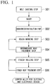
- FIG. 1 is a flowchart of a method of producing the copper alloy for an electronic and electric device of an embodiment of the present invention.
- a copper alloy for an electronic and electric device which is an embodiment of the present invention, is explained below.
- the copper alloy for an electronic and electric device of the present embodiment has a composition including: Mg in the range of 0.15 mass% or more and less than 0.35 mass%; and the Cu balance including inevitable impurities.
- the electrical conductivity is set to more than 75%IACS in the copper alloy for an electronic and electric device of the present embodiment.
- a strength ratio TS TD /TS LD which is calculated from strength TS TD obtained in a tensile test performed in a direction perpendicular to a rolling direction and strength TS LD obtained in a tensile test performed in a direction parallel to a rolling direction, is more than 0.9 and less than 1.1 in the copper alloy for an electronic and electric device of the present embodiment.
- the present embodiment is a rolled material of a copper alloy for electronic and electrical devices, and the relationship between the strength TS TD obtained in a tensile test performed in a direction perpendicular to a rolling direction and the strength TS LD obtained in a tensile test performed in a direction parallel to a rolling direction in the final step in rolling is defined as described above.
- the copper alloy further includes P in a range of 0.0005 mass% or more and less than 0.01 mass%.
- the Mg content [Mg] in a mass% and the P content [P] in a mass% satisfy a relational expression of [Mg]+20 ⁇ [P] ⁇ 0.5.
- the Mg content [Mg] in mass% and the P content [P] in mass% satisfy a relational expression of [Mg]/[P] ⁇ 400.
- a ratio of crystals having a crystal orientation within 10° with respect to a Brass orientation ⁇ 110 ⁇ ⁇ 112> is set to 40% or less
- a ratio of crystals having a crystal orientation within 10° with respect to a Copper orientation ⁇ 112 ⁇ ⁇ 111> is set to 40% or less.
- the Mg content is less than 0.15 mass%, there would be a possibility that the above-described effect cannot be obtained sufficiently.
- the alloy composition becomes close to the pure copper, the texture of the pure copper type is strongly formed after the finish rolling, and the ratio of the Copper orientation, which is a representative pure copper type orientation, which will be described later, becomes excessively high. Therefore, there would be a possibility that the strength ratio TS TD /TS LD becomes smaller value than the above-described appropriate range.
- the Mg content is set to the range of 0.15 mass% or more and less than 0.35 mass% in the present embodiment.
- the lower limit of the Mg content is set 0.18 mass% or more. It is more preferable that the lower limit of the Mg content is set to 0.2 mass% or more. In addition, it is preferable that the upper limit of the Mg content is set to 0.32 mass% or less. It is more preferable that the upper limit of the Mg content is set to 0.3 mass% or less.
- P is an element having effect of improving castability.
- P has a function of miniaturizing re-crystalized crystal grains by forming a compound with Mg.
- the P content is set to the range of 0.0005 mass% or more and less than 0.01 mass% in the present embodiment of adding P.
- the lower limit of the P content is set to 0.0007 mass% or more. It is more preferable that the lower limit of the P content is set to 0.001 mass% or more.
- the upper limit of the P content is set to less than 0.009 mass%. It is more preferable that the upper limit of the P content is set to less than 0.008 mass%. It is most preferable that the upper limit of the P content is set to less than 0.0075 mass%.
- the precipitates containing Mg and P are formed by having Mg and P coexist.
- [Mg]+20 ⁇ [P] is set to less than 0.5 in the present embodiment of adding P.
- [Mg]+20 ⁇ [P] is set to less than 0.48. It is more preferable that [Mg]+20 ⁇ [P] is set to less than 0.46.
- Mg is an element having effect of increasing the viscosity of the copper alloy melt and reducing the castability.
- [Mg]/[P] is set to 400 or less in the present embodiment of adding P. In order to further improve the castability, it is preferable that [Mg]/[P] is set to 350 or less. It is more preferable that [Mg]/[P] is set to 300 or less.
- the lower limit of [Mg]/[P] is set to a value exceeding 20. It is more preferable that the lower limit of [Mg]/[P] is set to a value exceeding 25.
- the total amount of these inevitable impurities is set to 0.1 mass% or less since they have action to reduce electrical conductivity. It is preferable that the total content of the inevitable impurities is set to 0.09 mass% or less. It is more preferable that the total content of the inevitable impurities is set to 0.08 mass% or less.
- the total amount of Ag, Zn, and Sn is set to less than 500 mass ppm.
- Si, Cr, Ti, Zr, Fe and Co particularly reduce the electrical conductivity significantly and deteriorate the bendability by forming inclusion bodies.
- the total amount of Si, Cr, Ti, Zr, Fe, and Co is set to less than 500 mass ppm.
- the strength ratio TS TD /TS LD which is calculated from strength TS TD obtained in a tensile test performed in a direction perpendicular to a rolling direction and strength TS LD obtained in a tensile test performed in a direction parallel to a rolling direction, is more than 0.9 and less than 1.1, there is less strong anisotropy; a sufficient strength is secured even in the case requiring strength in both of the LD direction and the TD direction such as in terminals and busbars for high current usage; and occurrence of cracking or the like, which occurs by unnecessary high-strengthening in a specific direction, in bending work can be suppressed.
- the copper alloy can obtain excellent bendability in bending in a direction in which the bending axis is perpendicular to the rolling direction (GW bending) and in bending in a direction in which the bending axis is parallel to the rolling direction (BW bending).
- the lower limit of the strength ratio TS TD /TS LD is set to 0.94 or more in order to reliably obtain these technical effects. More preferably, it is set to 0.98 or more. In addition, it is preferable to set the upper limit of the strength ratio TS TD /TS LD to 1.08 or less. More preferably, it is set to 1.06 or less.
- the copper alloy for an electronic or electric device of the present embodiment can be suitably used as a component for an electronic or electric device such as: terminals of connectors, press-fits, or the like; relays; lead frames; busbars; and the like by setting the electric conductivity to a value exceeding 75%IACS.
- the electrical conductivity is set to more than 76%IACS. More preferably, it is more than 77%IACS. Even more preferably, it is more than 78%IACS. Even more preferably, it is more than 80%IACS.
- the ratio of the crystals having a crystal orientation within 10° with respect to the Brass orientation ⁇ 110 ⁇ ⁇ 112> is set to 40% or less in order to suppress the anisotropy of the strength.
- the ratio of crystals having a crystal orientation within 10° with respect to the Brass orientation ⁇ 110 ⁇ ⁇ 112> is preferably set to 30% or less, more preferably 20% or less in order to further suppress the anisotropy of the strength.
- the lower limit of the ratio of crystals having a crystal orientation within 10° with respect to the Brass orientation ⁇ 110 ⁇ ⁇ 112> is preferably set to 1% or more, and more preferably to 5% or more.
- the ratio of the crystal having a crystal orientation within 10° with respect to the Copper orientation ⁇ 112 ⁇ ⁇ 111> is set to 40% or less in order to suppress the anisotropy of the strength.
- the ratio of crystals having a crystal orientation within 10° with respect to the Copper orientation ⁇ 112 ⁇ ⁇ 111> is preferably set to 30% or less, more preferably 20% or less in order to further suppress the anisotropy of the strength.
- the lower limit of the ratio of crystals having a crystal orientation within 10° with respect to the Copper orientation ⁇ 112 ⁇ ⁇ 111> is preferably set to 1% or more, and more preferably to 5% or more.
- components are adjusted by adding the above-described elements to molten copper obtained by melting a copper raw material, thereby producing a molten copper alloy.
- the molten copper is preferably a so-called 4NCu having purity set to 99.99% by mass or more: or a so-called 5NCu having purity set to 99.999% by mass or more.
- each of elements added it is possible to use a single body of the element, an alloy of the element, or the like.
- a raw material including the element may be melted together with the copper raw material.
- a recycled material or a scrapped material of the present alloy may also be used.
- the melting step it is preferable to perform atmosphere melting in an inert gas atmosphere with a low vapor pressure of H 2 O and keep the retention time in melting to the minimum in order to suppress oxidation of Mg; and reduce the hydrogen concentration.
- the ingot is produced by pouring the copper alloy melt with the adjusted component composition.
- the continuous casting method or the semi-continuous casting method is used.
- the cooling rate of the melt is set to 0.1°C/sec or more. More preferably, it is set to 0.5°C/sec or more. Most preferably, it is set to 1°C/sec or more.
- a heating treatment is carried out in order for homogenization of the obtained ingot and formation of a solid solution.
- an intermetallic compound including Cu and Mg as major components which is generated by Mg being condensed due to segregation in a solidification step is present inside the ingot. Therefore, in order to remove or reduce the segregation and the intermetallic compound, a heating treatment in which the ingot is heated to a temperature in a range of 300°C to 900°C is carried out, thereby homogeneously dispersing Mg or dissolving Mg in the matrix in the ingot. Meanwhile, this homogenization/solution treatment step S02 is preferably carried out in a non-oxidizing or reducing atmosphere.
- the heating temperature is lower than 300°C, formation of a solid solution becomes incomplete, and there is a concern that a large amount of an intermetallic compound including Cu and Mg as major components may remain in the matrix.
- the heating temperature exceeds 900°C, some of the copper material turns into a liquid phase, and there is a concern that the structure or the surface state may become uneven. Therefore, the heating temperature is set in a range of 300°C to 900°C.
- Hot working may be performed after the above-described homogenization/solution treatment step S02 for efficient rough working which is described below and homogenization of the structure.
- the processing method is not particularly limited. For example, rolling, drawing, extrusion, groove rolling, forging, pressing, or the like can be used.
- the temperature of hot working is set to the range of 300°C or more and 900°C or less.
- the temperature condition in the rough working step S03 is not particularly limited. However, it is preferable that the temperature condition is set to the range of -200°C to 200°C, which corresponds to cold or warm rolling, in order to suppress recrystallization or to improve dimensional accuracy. It is particularly preferable that the temperature condition is a room temperature. It is preferable that the processing ratio (the rolling ratio) is 20% or more. More preferably, it is 30% or more.
- the processing method is not particularly limited. For example, rolling, drawing, extrusion, groove rolling, forging, pressing, or the like can be used
- a heat treatment is carried out for softening, which aims to reliably form a solid solution, form a recrystallized structure or improve working properties.
- a method for the heat treatment is not particularly limited; however, preferably, the heat treatment is carried out: at a holding temperature of 400°C to 900°C; for a retention time of 10 seconds or more and 10 hours or less; in a non-oxidizing atmosphere or a reducing atmosphere.
- the cooling method after heating is not particularly limited. However, it is preferable that a method such as the water quenching and the like having the cooling rate of 200°C/min or more is used.
- the rough working step S03 and the Intermediate heat treatment step S04 may be repeatedly carried out.
- the copper material which has been subjected to the Intermediate heat treatment step S04 is finish-worked in order to be worked into a predetermined shape.
- the temperature condition in the finish working step S05 is not particularly limited. However, it is preferable that the temperature condition is set to the range of -200°C to 200°C, which corresponds to cold or warm rolling, in order to suppress recrystallization or softening. It is particularly preferable that the temperature condition is the room temperature.
- the processing rate is appropriately selected so that the copper alloy approximates to a final shape.
- the processing ratio is preferably set to 20% or more.
- the processing ratio is more preferably set to 30% or more. Even more preferably, it is set to 40% or more.
- the processing ratio in order to suppress the excessive orientation of the Brass orientation and the Copper orientation, it is preferable to set the processing ratio at 75% or less, more preferably the processing ratio at 70% or less.
- a finish heat treatment is carried out on the plastically-worked material obtained using the Finish working step S05 in order to improve the stress relaxation resistance and to obtain the effect of the low temperature annealing hardening; or to remove the residual strains.
- the heat treatment temperature is set in the range of 100°C or more and 600°C or less. More preferably, it is set in the range of 200°C or more and 500°C or less. Meanwhile, in the Finish heat treatment step S06, it is necessary to set heat treatment conditions (temperature, time, and cooling rate) so as to prevent the significant decrease of the strength due to recrystallization.
- This heat treatment is preferably carried out in a non-oxidizing atmosphere or a reducing atmosphere.
- the method of the heat treatment is not particularly limited. However, a short time heat treatment with the continuous annealing furnace is preferable in view of the effect of reducing the production cost.
- finish working step S05 and the finish heat treatment S06 may be repeatedly carried out.
- the plastically-worked copper alloy material for an electronic and electric device and the rolled plate (thin plate) of the present embodiment are produced.
- the plate thickness of the plastically-worked copper alloy material for an electronic and electric device (thin plate) is set to the range of more than 0.05 mm to 3.0 mm or less. Preferably, the thickness is set to the range of more than 0.1 mm to less than 3.0 mm.
- a plastically-worked copper alloy material for an electronic and electric device (thin plate) having a thickness of less than 0.05 mm is not suitable for using as a conductive body in the high current application. In a plastically-worked copper alloy material for an electronic and electric device (thin plate) having a thickness of more than 3.0 mm, the press punching processing becomes difficult.
- the plastically-worked copper alloy material for an electronic and electric device of the present invention may be used as a component for an electronic and electric device directly.
- a Sn plating layer or a Ag plating layer having the film thickness of 0.1-100 ⁇ m may be formed on one or both sides of the plate surfaces.
- the plate thickness of the plastically-worked copper alloy material for an electronic and electric device is 10-1000 times of the thickness of the plating layer.
- the component for an electronic and electric device such as terminals of connectors, press-fits, or the like; relays; lead frames; bus bars; and the like, is formed by performing punching processing, bending, or the like using the copper alloy for an electronic and electric device of the present embodiment as the material.
- the strength and the stress relaxation resistance can be improved without significantly reducing the electrical conductivity by solid soluting Mg in the copper matrix since the Mg content is set to the range of 0.15 mass% or more and less than 0.35 mass%.
- the conductivity is set to 75%IACS or more in the copper alloy for an electronic and electric device of the present embodiment. Thus, it can be applied to applications in which high conductivity is needed.
- the strength ratio TS TD /TS LD which is calculated from strength TS TD obtained in a tensile test performed in a direction perpendicular to a rolling direction and strength TS LD obtained in a tensile test performed in a direction parallel to the rolling direction, is more than 0.9 and less than 1.1.
- the copper alloy can obtain excellent bendability in bending in a direction in which the bending axis is perpendicular to the rolling direction (GW bending) and in bending in a direction in which the bending axis is parallel to the rolling direction (BW bending). Because of these, the copper alloy can obtain excellent bendability in bending in a direction in which the bending axis is perpendicular to the rolling direction (GW bending) and in bending in a direction in which the bending axis is parallel to the rolling direction (BW bending).
- the ratio between the content of Mg, which reduces the castability, and the content of P, which improves the castability, is optimized since the Mg content [Mg] in mass% and the P content [P] in mass% satisfy the relational expression of [Mg]/[P] ⁇ 400 in the present embodiment. Accordingly, because of the effect of adding P, the castability can be reliably improved.
- the ratio of crystals having a crystal orientation within 10° with respect to a Brass orientation ⁇ 110 ⁇ ⁇ 112> is set to 40% or less
- the ratio of crystals having a crystal orientation within 10° with respect to a Copper orientation ⁇ 112 ⁇ ⁇ 111> is set to 40% or less.
- the plastically-worked copper alloy material for an electronic and electric device of the present embodiment is made of the above-described copper alloy for an electronic and electric device, a component for an electronic and electric device such as terminals of connectors, press-fits, or the like; relays; lead frames; bus bars; and the like can be produced by performing bending or the liken on this plastically-worked copper alloy material for an electronic and electric device.
- the plastically-worked copper alloy material is particularly suitable for the material of the component for an electronic and electric device such as terminals of connectors, press-fits, or the like; relays; lead frames; bus bars; and the like
- the component for an electronic and electric device of the present embodiment (such as terminals of connectors, press-fits, or the like; relays; lead frames; bus bars; and the like) is made of the above-described copper alloy for an electronic and electric device, it can exhibit excellent properties even if it is down-sized and thinned.
- the copper alloy for an electronic and electric device the plastically-worked copper alloy material for an electronic and electric device, and the component (terminals, and busbars), which are embodiments of the present invention, have been described, but the present invention is not limited thereto and can be appropriately modified within the scope of the technical concept of the invention.
- the production methods are not limited to the present embodiments, and the copper alloy for an electronic and electric device may be produced by appropriately selecting an existing manufacturing method.
- the copper raw material made of oxygen-free copper (ASTM B152 C10100) having the purity of 99.99 mass% or more was prepared. Then, the copper raw material was inserted in a high purity graphite crucible and subjected to high frequency melting in an atmosphere furnace of Ar gas atmosphere. Then, each of additive elements was added in the obtained copper melt to prepare the component compositions shown in Table 1. By pouring the prepared copper melt in a mold, the ingot was produced. In Example 4 of the present invention and Comparative Example 6, a mold made of an insulation material (ISOWOOL) was used. In Example 14 of the present invention, a carbon mold was used.
- ISOWOOL insulation material
- Example 1-3, 5-13, 15-30 of the present invention and Comparative Examples 1-5 a copper alloy mold with water-cooling function was used as the mold for casting.
- the dimensions of ingots were about 20 mm for the thickness; about 150 mm for the width; and about 70 mm for the length.
- a portion near the cast surface was subjected to face working; and the ingot was cut out for the size to be adjusted in such a way that the plate thickness of the final product became 0.5 mm.
- This block was heated in an Ar gas atmosphere for four hours under a temperature condition shown in Table 2, thereby carrying out a homogenization/solution treatment.
- the copper material that had been subjected to the heat treatment was appropriately cut in order to form a shape suitable as the final shape, and surface grinding was carried out in order to remove an oxide layer. After that,
- finish rolling was carried out in the rolling ratio shown in Table 2 at the room temperature, and a thin plate having the thickness of 0.5 mm, the width of about 150 mm, and the length of 200 mm was produced.
- finish heat treatment was carried out in an Ar atmosphere under a condition shown in Table 2, and then water quenching was carried out, thereby producing a thin plate for characteristic evaluation.
- the depth of rough surface means the depth of the rough surface from the end part toward the central part of the ingot.
- No. 13B test specimen regulated by JIS Z 2241 was sampled from a strip material for characteristic evaluation, and the 0.2% yield strength was measured using the offset method of JIS Z 2241. The test specimen was sampled in the directions perpendicular and parallel to the rolling direction. Then, the strength ratio TS TD /TS LD was calculated from the obtained strength TS TD and TS LD . Evaluation results are shown in Table 3.
- test specimen having a width of 10 mm and a length of 150 mm was sampled from the strip material for characteristic evaluation, and the electrical resistance was obtained using a four-terminal method.
- the dimensions of the test specimen were measured using a micrometer, and the volume of the test specimen was computed.
- the electrical conductivity was calculated from the measured electric resistance and the volume. Meanwhile, the test specimen was sampled so that the longitudinal direction of the test specimen became perpendicular to the rolling direction of the strip material for characteristic evaluation.
- a surface perpendicular to the width direction of rolling that is, a TD (transverse direction) surface was used as an observation surface.
- TD transverse direction
- the Brass orientation ratio and the Copper orientation ratio were measured.
- the ratio of the Brass orientation (area ratio of the crystal orientation) and the ratio of the Copper orientation (area ratio of the crystal orientation) in the measurement area were obtained.
- a copper alloy for an electronic and electric device Compared to the conventional technologies, a copper alloy for an electronic and electric device; a plastically-worked copper alloy material for an electronic and electric device; a component for an electronic and electric device; a terminal; and a busbar, each of which has excellent electrical conductivity, strength, bendability, stress relaxation resistance and castability, can be provided.
Abstract
Description
- The present invention relates to a copper alloy for an electronic and/or electric device (electronic/electric device), which is suitable for terminals such as lead frames, connectors, press-fits and the like; a plastically-worked copper alloy material for an electronic and electric device made of the copper alloy for an electronic and electric device; a component for an electronic and electric device; a terminal; and a busbar.
- Priority is claimed on Japanese Patent Application No.
2015-177743, filed September 9, 2015 2015-235096, filed December 1, 2015 2016-069178, filed March 30, 2016 - Conventionally, highly conductive copper or copper alloy is used for an electronic or electric device such as terminals of connectors, press-fits, or the like; relays; lead frames; bus bars; and the like.
- In response to the size reduction of an electronic, an electric device, and the like, there have been attempts to reduce the size and thickness of components for an electronic and electric device used in the electronic device and electric device. Therefore, high strength and excellent bendability are required for the material constituting the component of the electronic or electric device.
- Furthermore, in large terminals and bus bars to which a large current is applied, it is necessary to use a rolling material with less anisotropy.
- For example, Cu-Mg alloys are proposed in Patent Literatures 1 and 2 (PTLs 1 and 2) as a material used for the electronic and electric device such as terminals; relays; lead frames; busbars; and the like.
-
- [PTL 1] Japanese Unexamined Patent Application, First Publication No.
2014-025089 (A - [PTL 2] Japanese Unexamined Patent Application, First Publication No.
2014-114464 (A - In the Cu-Mg-based alloy described in PTL 1, since the content of Mg is high, conductivity is insufficient and it is difficult to apply the alloy to applications requiring high conductivity.
- In addition, coarse precipitates are formed in the Cu-Mg alloy described in PTL 2 since the Mg content is 0.01-0.5 mass% and the P content is 0.01-0.5 mass%. Thus, the cold workability and the bendability are insufficient.
- The present invention is made under the circumstances described above. The purpose of the present invention is to provide a copper alloy for an electronic/electric device, a plastically-worked copper alloy material for an electronic or electric device, a component for an electronic or electric device, a terminal, and a busbar, all of which have excellent electrical conductivity, strength, and bendability; and less anisotropy.
- In order to solve the above-described problem, a copper alloy for an electronic and electric device, which is an aspect of the present invention, (hereinafter, referred as "the copper alloy for an electronic and electric device of the present invention") is configured that the copper alloy for an electronic and electric device includes: Mg in a range of 0.15 mass% or more and less than 0.35 mass%; and a Cu balance including inevitable impurities, wherein
the electrical conductivity of the copper alloy is more than 75%IACS, and
a strength ratio TSTD/TSLD, which is calculated from strength TSTD obtained from a tensile test performed in a direction perpendicular to a rolling direction and strength TSLD obtained in a tensile test performed in a direction parallel to a rolling direction, is more than 0.9 and less than 1.1. - According to the copper alloy for an electronic and electric device configured as described above, the strength and the stress relaxation resistance can be improved without greatly decreasing the electrical conductivity by solid melting Mg in the Cu matrix phase since the Mg content is in the range of 0.15 mass% or more and less than 0.35 mass%. Specifically, since the conductivity is more than 75%IACS, it can be applied to applications requiring high conductivity.
- In addition, since a strength ratio TSTD/TSLD, which is calculated from strength TSTD obtained in a tensile test performed in a direction perpendicular to a rolling direction and strength TSLD obtained in a tensile test performed in a direction parallel to a rolling direction, is more than 0.9 and less than 1.1, there is less strong anisotropy; a sufficient strength is secured even in the case requiring strength in both of the LD direction and the TD direction such as in terminals and busbars for high current usage; and occurrence of cracking or the like, which occurs by unnecessary high-strengthening in a specific direction, in bending work can be suppressed. In other words, the copper alloy can obtain excellent bendability in bending in a direction in which the bending axis is perpendicular to the rolling direction (GW bending) and in bending in a direction in which the bending axis is parallel to the rolling direction (BW bending).
- In the copper alloy for electronic and electric device of the present invention, the copper alloy may further include P in a range of 0.0005 mass% or more and less than 0.01 mass%.
- In this case, by adding P, the viscosity of the molten copper alloy containing Mg can be lowered, and castability can be improved.
- In addition, in the case where the copper alloy for electronic and electric device of the present invention includes P in the above-described range, the Mg content [Mg] in a mass% and the P content [P] in a mass% may satisfy a relational expression of [Mg]+20×[P]<0.5.
- In this case, it is possible to suppress the formation of coarse crystals containing Mg and P, and to suppress the deterioration of cold workability and bendability.
- In addition, in the case where the copper alloy for electronic and electric device of the present invention includes P in the above-described range, the Mg content [Mg] in mass% and the P content [P] in mass%, may satisfy a relational expression of [Mg]/[P]≤400.
- In this case, the castability can be improved reliably by defining the ratio between the content of Mg, which reduces the castability, and the content of P, which improves the castability, as described above.
- In addition, in the copper alloy for electronic and electric device of the present invention, a ratio of crystals having a crystal orientation within 10° with respect to a Brass orientation {110} <112> may be 40% or less, and
a ratio of crystals having a crystal orientation within 10° with respect to a Copper orientation {112} <111> may be 40% or less. - As the Brass orientation increases, the strength (TSTD) in the BW direction (perpendicular to the rolling direction) increases; and as the Copper orientation increases, the strength (TSLD) in the GW direction (parallel to the rolling direction) increases. Therefore, by limiting the ratio of the crystal having the Brass orientation and the crystal having the Copper orientation to 40% or less, it is possible to suppress the increase in either the strength in the BW direction or the strength in the GW direction. Moreover, it is possible to improve the bendability in GW bending and BW bending.
- A plastically-worked copper alloy material for an electronic and electric device, which is other aspect of the present invention, (hereinafter, referred as "the plastically-worked copper alloy material for an electronic and electric device of the present invention") is made of the above-described copper alloy for an electronic and electric device.
- According to the plastically-worked copper alloy material configured as described above, the plastically-worked copper alloy material has excellent electrical conductivity, strength, bendability, and stress relaxation resistance, since it is made of the above-described copper alloy for an electronic and electric device. Thus, the plastically-worked copper alloy material is particularly suitable for the material of an electronic and electric device, such as: terminals of connectors, press-fits or the like; relays; lead frames; busbars, and the like.
- In the plastically-worked copper alloy material for an electronic and electric device of the present invention, a Sn plating layer or a Ag plating layer may be provided
- In this case, the plastically-worked copper alloy material is particularly suitable for the material of an electronic and electric device, such as: terminals of connectors, press-fits or the like; relays; lead frames; busbars and the like since the Sn plating layer or the Ag plating layer is provided on the surface of the plastically-worked copper alloy material. In the present invention, "the Sn plating" includes a Sn plating of the pure Sn and a plating of a Sn alloy; and "the Ag plating" includes a plating made of the pure Ag and a plating made of a Ag alloy.
- A component for an electronic and electric device, which is other aspect of the present invention, (hereinafter, referred as "the component for an electronic and electric device of the present invention") is made of the above-described plastically-worked copper alloy material for an electronic and electric device. The component for an electronic and electric device of the present invention includes: terminals of connectors, press-fits or the like; relays; lead frames; busbars and the like.
- The component for an electronic and electric device configured as described above can exhibit excellent properties even if it is down-sized and thinned since it is produced by using the plastically-worked copper alloy material described above.
- A terminal, which is other aspect of the present invention, (hereinafter, referred as "the terminal of the present invention") is made of the above-described plastically-worked copper alloy material for an electronic and electric device.
- The terminal configured as described above can exhibit excellent properties even if it is down-sized and thinned since it is produced by using the plastically-worked copper alloy material described above.
- A busbar, which is other aspect of the present invention, (hereinafter, referred as "the busbar of the present invention") is made of the above-described plastically-worked copper alloy material for an electronic and electric device.
- The busbar configured as described above can exhibit excellent properties even if it is down-sized and thinned since it is produced by using the plastically-worked copper alloy material described above.
- According to the present invention, a copper alloy for an electronic and electric device; a plastically-worked copper alloy material for an electronic and electric device; a component for an electronic and electric device; a terminal; and a busbar, each of which has excellent electrical conductivity, strength, and bendability; and less anisotropy, can be provided.
-
FIG. 1 is a flowchart of a method of producing the copper alloy for an electronic and electric device of an embodiment of the present invention. - A copper alloy for an electronic and electric device, which is an embodiment of the present invention, is explained below.
- The copper alloy for an electronic and electric device of the present embodiment has a composition including: Mg in the range of 0.15 mass% or more and less than 0.35 mass%; and the Cu balance including inevitable impurities.
- In addition, the electrical conductivity is set to more than 75%IACS in the copper alloy for an electronic and electric device of the present embodiment.
- In addition, a strength ratio TSTD/TSLD, which is calculated from strength TSTD obtained in a tensile test performed in a direction perpendicular to a rolling direction and strength TSLD obtained in a tensile test performed in a direction parallel to a rolling direction, is more than 0.9 and less than 1.1 in the copper alloy for an electronic and electric device of the present embodiment. That is, the present embodiment is a rolled material of a copper alloy for electronic and electrical devices, and the relationship between the strength TSTD obtained in a tensile test performed in a direction perpendicular to a rolling direction and the strength TSLD obtained in a tensile test performed in a direction parallel to a rolling direction in the final step in rolling is defined as described above.
- In the copper alloy for electronic and electric device of the present embodiment, the copper alloy further includes P in a range of 0.0005 mass% or more and less than 0.01 mass%.
- In the case where the copper alloy for electronic and electric device of the present embodiment includes P in the above-described range, the Mg content [Mg] in a mass% and the P content [P] in a mass% satisfy a relational expression of [Mg]+20×[P]<0.5.
- In addition, in the case where the copper alloy for electronic and electric device of the present embodiment includes P in the above-described range, the Mg content [Mg] in mass% and the P content [P] in mass% satisfy a relational expression of [Mg]/[P]≤400.
- In the copper alloy for electronic and electric device of the present embodiment, a ratio of crystals having a crystal orientation within 10° with respect to a Brass orientation {110} <112> is set to 40% or less, and a ratio of crystals having a crystal orientation within 10° with respect to a Copper orientation {112} <111> is set to 40% or less.
- Reasons for setting the component compositions, the crystal orientation and each of characteristics as described above are explained below.
- By dissolving Mg in matrix of the copper alloy, it is possible to improve the strength and the stress relaxation resistance without significantly reducing the conductivity.
- If the Mg content is less than 0.15 mass%, there would be a possibility that the above-described effect cannot be obtained sufficiently. In addition, since the alloy composition becomes close to the pure copper, the texture of the pure copper type is strongly formed after the finish rolling, and the ratio of the Copper orientation, which is a representative pure copper type orientation, which will be described later, becomes excessively high. Therefore, there would be a possibility that the strength ratio TSTD/TSLD becomes smaller value than the above-described appropriate range.
- On the other hand, when the content of Mg is 0.35 mass% or more, the conductivity reduces significantly, the brass type texture structure is formed after finish rolling, and the Brass orientation ratio described later becomes excessively high. Therefore, there would be a possibility that the strength ratio TSTD/TSLD becomes larger value than the above-described appropriate range.
- Moreover, there would be a possibility that the electrical conductivity is significantly reduced and the viscosity of the melted copper alloy is increased and the castability is reduced.
- Accordingly, the Mg content is set to the range of 0.15 mass% or more and less than 0.35 mass% in the present embodiment.
- In order to reliably improve the above-described technical effects, it is preferable that the lower limit of the Mg content is set 0.18 mass% or more. It is more preferable that the lower limit of the Mg content is set to 0.2 mass% or more. In addition, it is preferable that the upper limit of the Mg content is set to 0.32 mass% or less. It is more preferable that the upper limit of the Mg content is set to 0.3 mass% or less.
- P is an element having effect of improving castability. In addition, P has a function of miniaturizing re-crystalized crystal grains by forming a compound with Mg.
- If the P content were less than 0.0005 mass%, there would be a possibility that the above-described effect cannot be obtained sufficiently. On the other hand, if the P content were 0.01 mass% or more, there would be a possibility that cracking occurs in cold working or bending since above-described precipitates containing Mg and P are coarsened; and these precipitates become start points of breakage.
- Accordingly, the P content is set to the range of 0.0005 mass% or more and less than 0.01 mass% in the present embodiment of adding P. In order to reliably improve the castability, it is preferable that the lower limit of the P content is set to 0.0007 mass% or more. It is more preferable that the lower limit of the P content is set to 0.001 mass% or more. In addition, in order to reliably suppress formation of the coarse precipitates, it is preferable that the upper limit of the P content is set to less than 0.009 mass%. It is more preferable that the upper limit of the P content is set to less than 0.008 mass%. It is most preferable that the upper limit of the P content is set to less than 0.0075 mass%.
- In the case of adding P, as described above, the precipitates containing Mg and P are formed by having Mg and P coexist.
- If the value of [Mg]+20×[P] were 0.5 or more where [Mg] is the Mg content and [P] is the P content in mass%, there would be a possibility that cracking occurs in cold working or bending since the total amount of Mg and P is excessive; the precipitates containing Mg and P are coarsened and distributed in high density.
- Accordingly, [Mg]+20×[P] is set to less than 0.5 in the present embodiment of adding P. In order to reliably suppress the coarsening and high-densification of the precipitates and formation of cracking in cold working or bending, it is preferable that [Mg]+20×[P] is set to less than 0.48. It is more preferable that [Mg]+20×[P] is set to less than 0.46.
- In order to reliably improve castability, it is necessary for the ratio of the Mg and P contents to be optimized since Mg is an element having effect of increasing the viscosity of the copper alloy melt and reducing the castability.
- If [Mg]/[P] exceeded 400 where [Mg] is the Mg content and [P] is the P content in mass%, there would be a possibility that the effect of improving the castability by adding P is reduced since the Mg content relative to P is increased.
- Accordingly, [Mg]/[P] is set to 400 or less in the present embodiment of adding P. In order to further improve the castability, it is preferable that [Mg]/[P] is set to 350 or less. It is more preferable that [Mg]/[P] is set to 300 or less.
- If [Mg]/[P] were excessively low, there would be a possibility that Mg is consumed as the precipitates; and the effect because of solid soluting of Mg cannot be obtained. In order to reliably improve the yield strength and the stress relaxation resistance because of solid soluting of Mg by suppressing the formation of the precipitates containing Mg and P, it is preferable that the lower limit of [Mg]/[P] is set to a value exceeding 20. It is more preferable that the lower limit of [Mg]/[P] is set to a value exceeding 25.
- As other inevitable impurities, Ag; B; Ca; Sr; Ba; Sc; Y; rare earth elements; Ti; Zr; Hf; V; Nb; Ta; Cr; Mo; W; Mn; Re; Fe; Ru; Os; Co; Se; Te; Rh; Ir; Ni; Pd; Pt; Au; Zn; Cd; Hg; Al; Ga; In; Ge; Sn; As; Sb; Tl; Pb; Bi; Be; N; C; Si; Li; H; O; S; or the like can be named. The total amount of these inevitable impurities is set to 0.1 mass% or less since they have action to reduce electrical conductivity. It is preferable that the total content of the inevitable impurities is set to 0.09 mass% or less. It is more preferable that the total content of the inevitable impurities is set to 0.08 mass% or less.
- Since Ag, Zn, and Sn are easily dissolved in Cu for the electrical conductivity to be reduced, it is preferable that the total amount of Ag, Zn, and Sn is set to less than 500 mass ppm.
- Moreover, Si, Cr, Ti, Zr, Fe and Co particularly reduce the electrical conductivity significantly and deteriorate the bendability by forming inclusion bodies. Thus, it is preferable that the total amount of Si, Cr, Ti, Zr, Fe, and Co is set to less than 500 mass ppm.
- In the case where the strength ratio TSTD/TSLD, which is calculated from strength TSTD obtained in a tensile test performed in a direction perpendicular to a rolling direction and strength TSLD obtained in a tensile test performed in a direction parallel to a rolling direction, is more than 0.9 and less than 1.1, there is less strong anisotropy; a sufficient strength is secured even in the case requiring strength in both of the LD direction and the TD direction such as in terminals and busbars for high current usage; and occurrence of cracking or the like, which occurs by unnecessary high-strengthening in a specific direction, in bending work can be suppressed. Because of these, the copper alloy can obtain excellent bendability in bending in a direction in which the bending axis is perpendicular to the rolling direction (GW bending) and in bending in a direction in which the bending axis is parallel to the rolling direction (BW bending).
- It is preferable that the lower limit of the strength ratio TSTD/TSLD is set to 0.94 or more in order to reliably obtain these technical effects. More preferably, it is set to 0.98 or more. In addition, it is preferable to set the upper limit of the strength ratio TSTD/TSLD to 1.08 or less. More preferably, it is set to 1.06 or less.
- The copper alloy for an electronic or electric device of the present embodiment can be suitably used as a component for an electronic or electric device such as: terminals of connectors, press-fits, or the like; relays; lead frames; busbars; and the like by setting the electric conductivity to a value exceeding 75%IACS.
- It is preferable that the electrical conductivity is set to more than 76%IACS. More preferably, it is more than 77%IACS. Even more preferably, it is more than 78%IACS. Even more preferably, it is more than 80%IACS.
- As the Brass orientation increases, the strength in the BW direction increases. Therefore, the ratio of the crystals having a crystal orientation within 10° with respect to the Brass orientation {110} <112> is set to 40% or less in order to suppress the anisotropy of the strength.
- The ratio of crystals having a crystal orientation within 10° with respect to the Brass orientation {110} <112> is preferably set to 30% or less, more preferably 20% or less in order to further suppress the anisotropy of the strength.
- On the other hand, if the ratio of the Brass orientation were too low, the strength in the BW direction would become too low and there would be a possibility that the required strength cannot be obtained. Thus, the lower limit of the ratio of crystals having a crystal orientation within 10° with respect to the Brass orientation {110} <112> is preferably set to 1% or more, and more preferably to 5% or more.
- As the Copper orientation increases, the strength in the GW direction increases. Therefore, the ratio of the crystal having a crystal orientation within 10° with respect to the Copper orientation {112} <111> is set to 40% or less in order to suppress the anisotropy of the strength.
- The ratio of crystals having a crystal orientation within 10° with respect to the Copper orientation {112} <111> is preferably set to 30% or less, more preferably 20% or less in order to further suppress the anisotropy of the strength.
- On the other hand, if the ratio of the Copper orientation were too low, the strength in the GW direction would become too low and there would be a possibility that the required strength cannot be obtained. Thus, the lower limit of the ratio of crystals having a crystal orientation within 10° with respect to the Copper orientation {112} <111> is preferably set to 1% or more, and more preferably to 5% or more.
- Next, a method of producing a copper alloy for an electronic and electric device of the present embodiment as configured above is explained in reference to the flowchart in
FIG. 1 . - First, components are adjusted by adding the above-described elements to molten copper obtained by melting a copper raw material, thereby producing a molten copper alloy. Here, the molten copper is preferably a so-called 4NCu having purity set to 99.99% by mass or more: or a so-called 5NCu having purity set to 99.999% by mass or more. Meanwhile, as each of elements added, it is possible to use a single body of the element, an alloy of the element, or the like.
- In addition, a raw material including the element may be melted together with the copper raw material. In addition, a recycled material or a scrapped material of the present alloy may also be used. In the melting step, it is preferable to perform atmosphere melting in an inert gas atmosphere with a low vapor pressure of H2O and keep the retention time in melting to the minimum in order to suppress oxidation of Mg; and reduce the hydrogen concentration.
- Then, the ingot is produced by pouring the copper alloy melt with the adjusted component composition. In consideration of mass production, it is preferable that the continuous casting method or the semi-continuous casting method is used.
- At this time, precipitates containing Mg and P are formed in solidification of the melt. Thus, by increasing the solidification rate, the size of the precipitates can be miniaturized further. Therefore, it is preferable that the cooling rate of the melt is set to 0.1°C/sec or more. More preferably, it is set to 0.5°C/sec or more. Most preferably, it is set to 1°C/sec or more.
- Next, a heating treatment is carried out in order for homogenization of the obtained ingot and formation of a solid solution. Inside the ingot, an intermetallic compound including Cu and Mg as major components which is generated by Mg being condensed due to segregation in a solidification step is present. Therefore, in order to remove or reduce the segregation and the intermetallic compound, a heating treatment in which the ingot is heated to a temperature in a range of 300°C to 900°C is carried out, thereby homogeneously dispersing Mg or dissolving Mg in the matrix in the ingot. Meanwhile, this homogenization/solution treatment step S02 is preferably carried out in a non-oxidizing or reducing atmosphere.
- Here, when the heating temperature is lower than 300°C, formation of a solid solution becomes incomplete, and there is a concern that a large amount of an intermetallic compound including Cu and Mg as major components may remain in the matrix. On the other hand, when the heating temperature exceeds 900°C, some of the copper material turns into a liquid phase, and there is a concern that the structure or the surface state may become uneven. Therefore, the heating temperature is set in a range of 300°C to 900°C.
- Hot working may be performed after the above-described homogenization/solution treatment step S02 for efficient rough working which is described below and homogenization of the structure. In this case, the processing method is not particularly limited. For example, rolling, drawing, extrusion, groove rolling, forging, pressing, or the like can be used. In addition, it is preferable that the temperature of hot working is set to the range of 300°C or more and 900°C or less.
- In order to shape the material into a predetermined shape, rough working is performed. The temperature condition in the rough working step S03 is not particularly limited. However, it is preferable that the temperature condition is set to the range of -200°C to 200°C, which corresponds to cold or warm rolling, in order to suppress recrystallization or to improve dimensional accuracy. It is particularly preferable that the temperature condition is a room temperature. It is preferable that the processing ratio (the rolling ratio) is 20% or more. More preferably, it is 30% or more. The processing method is not particularly limited. For example, rolling, drawing, extrusion, groove rolling, forging, pressing, or the like can be used
- After the rough working step S03, a heat treatment is carried out for softening, which aims to reliably form a solid solution, form a recrystallized structure or improve working properties. A method for the heat treatment is not particularly limited; however, preferably, the heat treatment is carried out: at a holding temperature of 400°C to 900°C; for a retention time of 10 seconds or more and 10 hours or less; in a non-oxidizing atmosphere or a reducing atmosphere. In addition, the cooling method after heating is not particularly limited. However, it is preferable that a method such as the water quenching and the like having the cooling rate of 200°C/min or more is used.
- Meanwhile, the rough working step S03 and the Intermediate heat treatment step S04 may be repeatedly carried out.
- The copper material which has been subjected to the Intermediate heat treatment step S04 is finish-worked in order to be worked into a predetermined shape. Meanwhile, the temperature condition in the finish working step S05 is not particularly limited. However, it is preferable that the temperature condition is set to the range of -200°C to 200°C, which corresponds to cold or warm rolling, in order to suppress recrystallization or softening. It is particularly preferable that the temperature condition is the room temperature. In addition, the processing rate is appropriately selected so that the copper alloy approximates to a final shape. However, in order to increase strength by means of work hardening; or by means of increasing the ratios of the Brass and Copper orientations, which are rolling textures in the finish working step S05, the processing ratio is preferably set to 20% or more. In addition, in a case in which additional improvement in the strength is required, the processing ratio is more preferably set to 30% or more. Even more preferably, it is set to 40% or more.
- On the other hand, in order to suppress the excessive orientation of the Brass orientation and the Copper orientation, it is preferable to set the processing ratio at 75% or less, more preferably the processing ratio at 70% or less.
- Next, a finish heat treatment is carried out on the plastically-worked material obtained using the Finish working step S05 in order to improve the stress relaxation resistance and to obtain the effect of the low temperature annealing hardening; or to remove the residual strains.
- If the heat treatment temperature were too high, the strength ratio TSTD/TSLD would be significantly reduced. Therefore, it is preferable that the heat treatment temperature is set in the range of 100°C or more and 600°C or less. More preferably, it is set in the range of 200°C or more and 500°C or less. Meanwhile, in the Finish heat treatment step S06, it is necessary to set heat treatment conditions (temperature, time, and cooling rate) so as to prevent the significant decrease of the strength due to recrystallization.
- For example, it is preferable that it is retained for roughly 1 second to 120 seconds at 350°C. This heat treatment is preferably carried out in a non-oxidizing atmosphere or a reducing atmosphere.
- The method of the heat treatment is not particularly limited. However, a short time heat treatment with the continuous annealing furnace is preferable in view of the effect of reducing the production cost.
- Furthermore, the above-described finish working step S05 and the finish heat treatment S06 may be repeatedly carried out.
- As described above, the plastically-worked copper alloy material for an electronic and electric device and the rolled plate (thin plate) of the present embodiment are produced. The plate thickness of the plastically-worked copper alloy material for an electronic and electric device (thin plate) is set to the range of more than 0.05 mm to 3.0 mm or less. Preferably, the thickness is set to the range of more than 0.1 mm to less than 3.0 mm. A plastically-worked copper alloy material for an electronic and electric device (thin plate) having a thickness of less than 0.05 mm is not suitable for using as a conductive body in the high current application. In a plastically-worked copper alloy material for an electronic and electric device (thin plate) having a thickness of more than 3.0 mm, the press punching processing becomes difficult.
- The plastically-worked copper alloy material for an electronic and electric device of the present invention may be used as a component for an electronic and electric device directly. Alternatively, a Sn plating layer or a Ag plating layer having the film thickness of 0.1-100 µm may be formed on one or both sides of the plate surfaces. At this time, it is preferable that the plate thickness of the plastically-worked copper alloy material for an electronic and electric device is 10-1000 times of the thickness of the plating layer.
- In addition, the component for an electronic and electric device such as terminals of connectors, press-fits, or the like; relays; lead frames; bus bars; and the like, is formed by performing punching processing, bending, or the like using the copper alloy for an electronic and electric device of the present embodiment as the material.
- According to the copper alloy for an electronic and electric device of the present embodiment configured as described above, the strength and the stress relaxation resistance can be improved without significantly reducing the electrical conductivity by solid soluting Mg in the copper matrix since the Mg content is set to the range of 0.15 mass% or more and less than 0.35 mass%.
- In addition, the conductivity is set to 75%IACS or more in the copper alloy for an electronic and electric device of the present embodiment. Thus, it can be applied to applications in which high conductivity is needed.
- In the copper alloy for electronic and electric devices according to the present embodiment, the strength ratio TSTD/TSLD, which is calculated from strength TSTD obtained in a tensile test performed in a direction perpendicular to a rolling direction and strength TSLD obtained in a tensile test performed in a direction parallel to the rolling direction, is more than 0.9 and less than 1.1. Thus, there is less strong anisotropy in the copper alloy; a sufficient strength is secured even in the case requiring strength in both of the LD direction and the TD direction such as in terminals and busbars for high current usage; and occurrence of cracking or the like, which occurs by unnecessary high-strengthening in a specific direction, in bending work can be suppressed. In other words, the copper alloy can obtain excellent bendability in bending in a direction in which the bending axis is perpendicular to the rolling direction (GW bending) and in bending in a direction in which the bending axis is parallel to the rolling direction (BW bending). Because of these, the copper alloy can obtain excellent bendability in bending in a direction in which the bending axis is perpendicular to the rolling direction (GW bending) and in bending in a direction in which the bending axis is parallel to the rolling direction (BW bending).
- In addition, in the case where P is added to the coper alloy for electronic and electrical device of the present embodiment; and the P content is set to the range of 0.0005 mass% or more and less than 0.01 mass%, castability can be improved by reducing viscosity of the copper alloy melt.
- In addition, formation of coarse precipitations containing Mg and P can be suppressed since the Mg content [Mg] in mass% and the P content [P] in mass% satisfy the relational expression of [Mg]+20×[P]<0.5. Accordingly, reduction of cold workability and bendability can be suppressed.
- Moreover, the ratio between the content of Mg, which reduces the castability, and the content of P, which improves the castability, is optimized since the Mg content [Mg] in mass% and the P content [P] in mass% satisfy the relational expression of [Mg]/[P]≤400 in the present embodiment. Accordingly, because of the effect of adding P, the castability can be reliably improved.
- In addition, in the present embodiment, the ratio of crystals having a crystal orientation within 10° with respect to a Brass orientation {110} <112> is set to 40% or less, and the ratio of crystals having a crystal orientation within 10° with respect to a Copper orientation {112} <111> is set to 40% or less. Thus, it is possible to further suppress the difference between the strength TSTD in a tensile test performed in a direction perpendicular to the rolling direction and the strength TSLD in a tensile test performed in a direction parallel to the rolling direction; and a copper alloy for electronic and electric devices with less anisotropy can be obtained.
- In addition, since the plastically-worked copper alloy material for an electronic and electric device of the present embodiment is made of the above-described copper alloy for an electronic and electric device, a component for an electronic and electric device such as terminals of connectors, press-fits, or the like; relays; lead frames; bus bars; and the like can be produced by performing bending or the liken on this plastically-worked copper alloy material for an electronic and electric device.
- In the case where the Sn plating layer or the Ag plating layer is formed on the surface, the plastically-worked copper alloy material is particularly suitable for the material of the component for an electronic and electric device such as terminals of connectors, press-fits, or the like; relays; lead frames; bus bars; and the like
- In addition, since the component for an electronic and electric device of the present embodiment (such as terminals of connectors, press-fits, or the like; relays; lead frames; bus bars; and the like) is made of the above-described copper alloy for an electronic and electric device, it can exhibit excellent properties even if it is down-sized and thinned.
- Thus far, the copper alloy for an electronic and electric device, the plastically-worked copper alloy material for an electronic and electric device, and the component (terminals, and busbars), which are embodiments of the present invention, have been described, but the present invention is not limited thereto and can be appropriately modified within the scope of the technical concept of the invention.
- For example, in the above-described embodiments, examples of the method for producing the copper alloy for an electronic and electric device has been described, but the production methods are not limited to the present embodiments, and the copper alloy for an electronic and electric device may be produced by appropriately selecting an existing manufacturing method.
- Hereinafter, results of confirmation tests carried out in order to confirm the effects of the present invention will be described.
- The copper raw material made of oxygen-free copper (ASTM B152 C10100) having the purity of 99.99 mass% or more was prepared. Then, the copper raw material was inserted in a high purity graphite crucible and subjected to high frequency melting in an atmosphere furnace of Ar gas atmosphere. Then, each of additive elements was added in the obtained copper melt to prepare the component compositions shown in Table 1. By pouring the prepared copper melt in a mold, the ingot was produced. In Example 4 of the present invention and Comparative Example 6, a mold made of an insulation material (ISOWOOL) was used. In Example 14 of the present invention, a carbon mold was used. In Examples 1-3, 5-13, 15-30 of the present invention and Comparative Examples 1-5, a copper alloy mold with water-cooling function was used as the mold for casting. The dimensions of ingots were about 20 mm for the thickness; about 150 mm for the width; and about 70 mm for the length.
- A portion near the cast surface was subjected to face working; and the ingot was cut out for the size to be adjusted in such a way that the plate thickness of the final product became 0.5 mm.
- This block was heated in an Ar gas atmosphere for four hours under a temperature condition shown in Table 2, thereby carrying out a homogenization/solution treatment.
- After that, the heat treatment was performed in the temperature condition shown in Table 2 by using a salt bath after performing the rough working in the condition shown in Table 2.
- The copper material that had been subjected to the heat treatment was appropriately cut in order to form a shape suitable as the final shape, and surface grinding was carried out in order to remove an oxide layer. After that,
- Next, finish rolling (finish work) was carried out in the rolling ratio shown in Table 2 at the room temperature, and a thin plate having the thickness of 0.5 mm, the width of about 150 mm, and the length of 200 mm was produced. In addition, after the finish rolling (finish work), a finish heat treatment was carried out in an Ar atmosphere under a condition shown in Table 2, and then water quenching was carried out, thereby producing a thin plate for characteristic evaluation.
- As an evaluation of castability, the presence or absence of rough surface during the above-described casting was observed. One having no visually recognized rough surface at all or one having almost no visually recognized rough surface was graded as "A." One with a minor rough surface with the depth of less than 1 mm was graded as "B." One with rough surface with the depth of 1 mm or more and less than 2 mm was graded as "C." One with a major rough surface with the depth of 2 mm or more was graded as "D". Evaluation results are shown in Table 3.
- The depth of rough surface means the depth of the rough surface from the end part toward the central part of the ingot.
- No. 13B test specimen regulated by JIS Z 2241 was sampled from a strip material for characteristic evaluation, and the 0.2% yield strength was measured using the offset method of JIS Z 2241. The test specimen was sampled in the directions perpendicular and parallel to the rolling direction. Then, the strength ratio TSTD/TSLD was calculated from the obtained strength TSTD and TSLD. Evaluation results are shown in Table 3.
- A test specimen having a width of 10 mm and a length of 150 mm was sampled from the strip material for characteristic evaluation, and the electrical resistance was obtained using a four-terminal method. In addition, the dimensions of the test specimen were measured using a micrometer, and the volume of the test specimen was computed. In addition, the electrical conductivity was calculated from the measured electric resistance and the volume. Meanwhile, the test specimen was sampled so that the longitudinal direction of the test specimen became perpendicular to the rolling direction of the strip material for characteristic evaluation.
- Evaluation results are shown in Table 3.
- Bending working was carried out on the basis of the method of Japan Copper and Brass Association Technical Standard JCBA-T307:2007, the testing method 4.
- A plurality of test specimens having a width of 10 mm and a length of 30 mm were sampled from the thin plate for characteristic evaluation so that the bending axis became perpendicular (GW bending) or parallel (BW bending) to the rolling direction; and a W bending test was carried out using a W-shaped jig having a bending angle of 90 degrees and a bending radius of 0.4 mm (R/t=0.8).
- The outer circumferential portion of the bent portion was visually observed, and a test specimen in which cracking was observed was graded as "C." A test specimen in which a major folding was observed was graded as "B." A test specimen with no observable folding was graded as "A." Grades A and B were regarded as acceptable bendability. Evaluation results are shown in Table 3.
- A surface perpendicular to the width direction of rolling, that is, a TD (transverse direction) surface was used as an observation surface. Using an EBSD measurement device and the OIM analysis software, the Brass orientation ratio and the Copper orientation ratio were measured.
- Mechanical polishing was performed using waterproof abrasive paper and diamond abrasive grains, and finish polishing was performed using a colloidal silica solution. Using an EBSD measurement device (QUANTA FEG 450 manufactured by FEI Company, OIM DATA COLLECTION manufactured by EDAX/TSL (at present, AMETEK Inc.)) and an analysis software (OIM DATA ANALYSIS Ver. 6.2 manufactured by EDAX/TSL (at present, AMETEK Inc.)), an orientation of each of crystal grains was analyzed under conditions of an acceleration voltage of electron beams of 20 kV, a measurement interval of 0.1 µm step, and a measurement area of 1000 µm2 or more. By determining whether each of crystal grains belonged to the targeted Brass orientation (within 10° from the ideal orientation) or not; and by determining whether each of crystal grains belonged to the targeted Copper orientation (within 10° from the ideal orientation) or not, the ratio of the Brass orientation (area ratio of the crystal orientation) and the ratio of the Copper orientation (area ratio of the crystal orientation) in the measurement area were obtained.
[Table 1] Mg (mass%) P (mass%) Cu [Mg]+20×[P] [Mg]/[P] 1 0.15 0.0023 balance 0.20 65 2 0.15 0.0000 balance 0.15 - 3 0.16 0.0083 balance 0.33 19 4 0.18 0.0047 balance 0.27 38 5 0.19 0.0028 balance 0.25 68 6 0.21 0.0000 balance 0.21 - 7 0.17 0.0004 balance 0.18 425 8 0.23 0.0006 balance 0.24 383 9 0.29 0.0009 balance 0.31 322 10 0.25 0.0076 balance 0.40 33 11 0.23 0.0083 balance 0.40 28 12 0.21 0.0092 balance 0.39 23 13 0.20 0.0108 balance 0.42 19 14 0.16 0.0061 balance 0.28 26 Example of 15 0.17 0.0043 balance 0.26 40 the present invention 16 0.18 0.0026 balance 0.23 69 17 0.31 0.0051 balance 0.41 61 18 0.32 0.0025 balance 0.37 128 19 0.32 0.0071 balance 0.46 45 20 0.24 0.0020 balance 0.28 120 21 0.25 0.0010 balance 0.27 250 22 0.25 0.0016 balance 0.28 156 23 0.26 0.0010 balance 0.28 260 24 0.25 0.0015 balance 0.28 167 25 0.31 0.0082 balance 0.47 38 26 0.32 0.0009 balance 0.34 356 27 0.33 0.0082 balance 0.49 40 28 0.34 0.0000 balance 0.34 - 29 0.34 0.0010 balance 0.36 340 30 0.33 0.0008 balance 0.35 413 Comparative Example 1 0.04 0.0013 balance 0.07 31 2 0.03 0.0000 balance 0.03 - 3 0.52 0.0000 balance 0.52 - 4 0.53 0.0068 balance 0.67 78 5 0.30 0.0036 balance 0.37 83 6 0.16 0.0094 balance 0.35 17 [Table 2] Casting Homogenization/ solution Rough working Intermediate heat treatment Finish rolling Finish heat treatment Cooling rate (°C/sec) Temperature (°C) Rolling ratio (%) Temperature (°C) Time (sec) Rolling ratio (%) Temperature (°C) Time (sec) 1 10 550 80 500 60 60 300 60 2 10 500 60 475 300 50 350 60 3 10 550 60 500 60 70 300 60 4 0.4 550 60 550 60 50 350 60 5 10 650 80 600 60 60 300 60 6 10 700 70 550 60 75 350 60 7 10 600 80 550 180 70 350 60 8 10 600 80 550 60 60 350 60 9 10 700 80 525 180 60 300 60 Example of the present invention 10 10 700 60 525 60 50 350 60 11 10 700 80 550 60 70 350 60 12 10 650 70 500 300 60 350 60 13 10 650 80 550 60 60 350 60 14 0.8 550 65 500 60 90 400 60 15 10 550 65 525 60 90 350 300 16 10 600 80 550 60 80 450 300 17 10 700 60 600 60 60 275 60 18 10 700 50 600 60 80 275 60 19 10 700 50 650 180 85 250 60 20 10 700 70 550 60 60 350 60 21 10 700 75 550 60 85 350 60 22 10 700 70 550 60 40 350 60 23 10 700 60 575 60 60 350 60 24 10 700 70 525 180 60 350 60 25 10 700 70 550 60 60 300 60 26 10 700 70 550 60 40 350 60 27 10 700 70 500 300 60 300 60 28 10 715 80 550 300 30 300 60 29 10 715 80 600 60 60 300 60 30 10 715 60 550 60 60 350 60 1 10 500 70 400 300 30 250 60 2 10 500 60 425 60 35 275 60 Comparative Example 3 10 715 80 575 300 50 350 60 4 10 715 50 650 60 60 350 60 5 10 700 60 650 300 90 200 60 6 0.4 550 50 500 60 90 510 60 [Table 3] Castability Copper orientation ratio (%) Brass orientation ratio (%) TSLD (MPa) TSTD (MPa) TSTD/TSLD Conductivity (%IACS) GW bending BW bending 1 A 14 7 412 421 1.02 89.2 A A 2 B 10 6 368 378 1.03 89.6 A A 3 A 16 10 432 428 0.99 87.6 A A 4 A 7 10 411 413 1.00 86.6 A A 5 A 9 11 421 432 1.03 86.0 A A 6 B 18 18 434 442 1.02 85.0 A A 7 B 9 12 412 410 1.00 87.2 A A 8 B 8 15 410 413 1.01 83.2 A A 9 B 9 16 448 461 1.03 79.8 A A 10 A 10 13 398 400 1.01 82.3 A A Example of the present invention 11 A 13 11 428 431 1.01 83.4 A A 12 A 12 9 406 398 0.98 84.3 A A 13 A 8 12 398 403 1.01 85.1 B B 14 A 37 19 463 421 0.91 88.2 B A 15 A 33 18 458 427 0.93 87.3 B A 16 A 30 19 438 400 0.94 86.8 A A 17 A 11 23 443 470 1.06 77.2 A A 18 A 15 31 477 516 1.08 78.3 A B 19 A 13 36 462 504 1.09 77.9 A B 20 A 8 12 408 421 1.03 82.7 A A 21 B 18 30 476 475 1.00 82.4 A A 22 A 4 9 376 371 0.99 82.6 A A 23 A 9 12 416 430 1.03 81.7 A A 24 A 6 13 410 423 1.03 82.3 A A 25 A 9 16 441 451 1.02 78.3 B B 26 B 5 13 381 389 1.02 78.0 A A 27 A 10 17 432 448 1.04 76.7 B B 28 B 5 11 384 392 1.02 75.8 A A 29 B 10 16 453 467 1.03 75.3 A A 30 B 11 15 425 438 1.03 76.8 A A 1 A 9 6 271 264 0.97 95.9 A A 2 B 10 7 279 268 0.96 96.0 A A Comparative Example 3 B 11 19 438 449 1.03 67.6 A A 4 A 13 28 458 469 1.02 67.2 A B 5 A 18 42 514 572 1.11 78.1 A C 6 A 41 23 431 381 0.88 90.2 C B - In Comparative Examples 1-2, the Mg content was lower than the range defined in the scope of the present invention; and the strength was insufficient.
- In Comparative Examples 3-4, the Mg content was higher than the range defined in the scope of the present invention; and the electrical conductivity was low.
- In Comparative Example 5, the strength ratio TSTD/TSLD was higher than the range in the scope of the present invention, and bendability in the case where the bending axis was perpendicular direction (GW bending) with respect to the rolling direction was insufficient.
- In Comparative Example 6, the strength ratio TSTD/TSLD was lower than the range in the scope of the present invention, and bendability in the case where the bending axis was parallel direction (BW bending) with respect to the rolling direction was insufficient.
- Contrary to that, it was confirmed that the strength, the electrical conductivity, and bendability were excellent; and there was less anisotropy, in Examples of the present invention.
- In addition, in the case of adding P, it was confirmed that castability was excellent in Examples of the present invention.
- Based on these results, it was confirmed by Examples of the present invention that copper alloy for an electronic and electric device and plastically-worked copper alloy for an electronic and electric device having: excellent electrical conductivity, strength, bendability and castability; and less anisotropy, were provided
- Compared to the conventional technologies, a copper alloy for an electronic and electric device; a plastically-worked copper alloy material for an electronic and electric device; a component for an electronic and electric device; a terminal; and a busbar, each of which has excellent electrical conductivity, strength, bendability, stress relaxation resistance and castability, can be provided.
Claims (10)
- A copper alloy for an electronic and electric device comprising:Mg in a range of 0.15 mass% or more and less than 0.35 mass%; anda Cu balance including inevitable impurities, whereinthe electrical conductivity of the copper alloy is more than 75%IACS, anda strength ratio TSTD/TSLD, which is calculated from strength TSTD obtained in a tensile test performed in a direction perpendicular to a rolling direction and strength TSLD obtained in a tensile test performed in a direction parallel to a rolling direction, is more than 0.9 and less than 1.1.
- The copper alloy for an electronic and electric device according to Claim 1, further comprising P in a range of 0.0005 mass% or more and less than 0.01 mass%.
- The copper alloy for an electronic and electric device according to Claim 2, wherein
the Mg content [Mg] in mass% and the P content [P] in mass% satisfy a relational expression of [Mg]+20×[P]<0.5. - The copper alloy for an electronic and electric device according to Claim 2 or 3, wherein
the Mg content [Mg] in mass% and the P content [P] in mass% satisfy a relational expression of [Mg]/[P]≤400. - The copper alloy for an electronic and electric device according to any one of Claims 1 to 4, wherein
a ratio of crystals having a crystal orientation within 10° with respect to a Brass orientation {110} <112> is 40% or less, and
a ratio of crystals having a crystal orientation within 10° with respect to a Copper orientation {112} <111> is 40% or less. - A plastically-worked copper alloy material for an electronic and electric device made of the copper alloy for an electronic and electric device according to any one of Claims 1 to 5.
- The plastically-worked copper alloy material for an electronic and electric device according to Claim 6, wherein a Sn plating layer or a Ag plating layer is provided on a surface of the plastically-worked copper alloy material.
- A component for an electronic and electric device made of the plastically-worked copper alloy material for an electronic and electric device according to Claim 6 or 7.
- A terminal made of the plastically-worked copper alloy material for an electronic and electric device according to Claim 6 or 7.
- A busbar made of the plastically-worked copper alloy material for an electronic and electric device according to Claim 6 or 7.
Applications Claiming Priority (4)
| Application Number | Priority Date | Filing Date | Title |
|---|---|---|---|
| JP2015177743 | 2015-09-09 | ||
| JP2015235096A JP5910790B1 (en) | 2015-12-01 | 2015-12-01 | Copper alloy for electronic and electric equipment, copper alloy plastic working material for electronic and electric equipment, parts for electronic and electric equipment, terminals, and bus bars |
| JP2016069178A JP6187630B1 (en) | 2016-03-30 | 2016-03-30 | Copper alloy for electronic and electric equipment, copper alloy plastic working material for electronic and electric equipment, parts for electronic and electric equipment, terminals, and bus bars |
| PCT/JP2016/076456 WO2017043577A1 (en) | 2015-09-09 | 2016-09-08 | Copper alloy for electronic/electrical device, copper alloy plastically worked material for electronic/electrical device, component for electronic/electrical device, terminal, and busbar |
Publications (3)
| Publication Number | Publication Date |
|---|---|
| EP3348659A1 true EP3348659A1 (en) | 2018-07-18 |
| EP3348659A4 EP3348659A4 (en) | 2019-05-22 |
| EP3348659B1 EP3348659B1 (en) | 2020-12-23 |
Family
ID=58239837
Family Applications (1)
| Application Number | Title | Priority Date | Filing Date |
|---|---|---|---|
| EP16844438.8A Active EP3348659B1 (en) | 2015-09-09 | 2016-09-08 | Copper alloy for electronic/electrical device, copper alloy plastically-worked material for electronic/electrical device, component for electronic/electrical device, terminal, and busbar |
Country Status (10)
| Country | Link |
|---|---|
| US (1) | US10676803B2 (en) |
| EP (1) | EP3348659B1 (en) |
| KR (1) | KR102474714B1 (en) |
| CN (1) | CN107636179B (en) |
| MX (1) | MX2018001139A (en) |
| MY (1) | MY196265A (en) |
| PH (1) | PH12017502293A1 (en) |
| SG (1) | SG11201710361SA (en) |
| TW (1) | TWI701351B (en) |
| WO (1) | WO2017043577A1 (en) |
Families Citing this family (8)
| Publication number | Priority date | Publication date | Assignee | Title |
|---|---|---|---|---|
| CN107208189B (en) | 2015-09-09 | 2020-08-04 | 三菱综合材料株式会社 | Copper alloy, copper alloy plastic working material, assembly, terminal, and bus bar |
| EP3348656B1 (en) * | 2015-09-09 | 2020-12-30 | Mitsubishi Materials Corporation | Copper alloy for electronic/electrical device, copper alloy plastically worked material for electronic/electrical device, component for electronic/electrical device, terminal, and busbar |
| WO2017170733A1 (en) | 2016-03-30 | 2017-10-05 | 三菱マテリアル株式会社 | Copper alloy for electronic and electrical equipment, copper alloy plate strip for electronic and electrical equipment, component for electronic and electrical equipment, terminal, busbar, and movable piece for relays |
| US11203806B2 (en) * | 2016-03-30 | 2021-12-21 | Mitsubishi Materials Corporation | Copper alloy for electronic and electrical equipment, copper alloy plate strip for electronic and electrical equipment, component for electronic and electrical equipment, terminal, busbar, and movable piece for relay |
| JP6780187B2 (en) | 2018-03-30 | 2020-11-04 | 三菱マテリアル株式会社 | Copper alloys for electronic / electrical equipment, copper alloy strips for electronic / electrical equipment, parts for electronic / electrical equipment, terminals, and busbars |
| KR20200134215A (en) * | 2018-03-30 | 2020-12-01 | 미쓰비시 마테리알 가부시키가이샤 | Copper alloy for electronic and electric equipment, copper alloy plate strip for electronic and electric equipment, parts for electronic and electric equipment, terminals, and busbars |
| CN110172609A (en) * | 2019-05-16 | 2019-08-27 | 红河学院 | A kind of high-strength high-conductivity copper magnesium system alloy and preparation method thereof |
| JP7024925B2 (en) * | 2019-11-29 | 2022-02-24 | 三菱マテリアル株式会社 | Copper alloys, plastic working materials for copper alloys, parts for electronic and electrical equipment, terminals, bus bars, heat dissipation boards |
Family Cites Families (33)
| Publication number | Priority date | Publication date | Assignee | Title |
|---|---|---|---|---|
| US3778318A (en) | 1969-02-24 | 1973-12-11 | Cooper Range Co | Copper base composition |
| US3677745A (en) * | 1969-02-24 | 1972-07-18 | Cooper Range Co | Copper base composition |
| JPS5910790B2 (en) | 1981-06-16 | 1984-03-12 | 東洋製罐株式会社 | How to separate citrus sandbags |
| JPS58199835A (en) | 1982-05-19 | 1983-11-21 | Sumitomo Electric Ind Ltd | Copper alloy for electric or electronic apparatus |
| JPS61284946A (en) | 1985-06-11 | 1986-12-15 | Mitsubishi Shindo Kk | Cu alloy lead blank for semiconductor device |
| JP2661462B2 (en) | 1992-05-01 | 1997-10-08 | 三菱伸銅株式会社 | Straight line excellent in repeated bending property: Cu alloy ultrafine wire of 0.1 mm or less |
| US5486244A (en) * | 1992-11-04 | 1996-01-23 | Olin Corporation | Process for improving the bend formability of copper alloys |
| JP3796784B2 (en) | 1995-12-01 | 2006-07-12 | 三菱伸銅株式会社 | Copper alloy thin plate for manufacturing connectors and connectors manufactured with the thin plates |
| US6632300B2 (en) * | 2000-06-26 | 2003-10-14 | Olin Corporation | Copper alloy having improved stress relaxation resistance |
| US20040238086A1 (en) | 2003-05-27 | 2004-12-02 | Joseph Saleh | Processing copper-magnesium alloys and improved copper alloy wire |
| JP4756197B2 (en) * | 2005-08-23 | 2011-08-24 | Dowaメタルテック株式会社 | Cu-Mg-P-based copper alloy and method for producing the same |
| US20100269963A1 (en) * | 2007-11-01 | 2010-10-28 | Kiyoshige Hirose | Copper alloy material excellent in strength, bending workability and stress relaxation resistance, and method for producing the same |
| JP5260992B2 (en) | 2008-03-19 | 2013-08-14 | Dowaメタルテック株式会社 | Copper alloy sheet and manufacturing method thereof |
| WO2009117639A2 (en) * | 2008-03-20 | 2009-09-24 | Interplex Nas, Inc. | Press fit (compliant) terminal and other connectors with tin-silver compound |
| JP5541651B2 (en) | 2008-10-24 | 2014-07-09 | 三菱マテリアル株式会社 | Sputtering target for wiring film formation for thin film transistors |
| JP5311283B2 (en) | 2009-03-11 | 2013-10-09 | 住友電気工業株式会社 | Nonaqueous electrolyte battery and manufacturing method thereof |
| JP4516154B1 (en) | 2009-12-23 | 2010-08-04 | 三菱伸銅株式会社 | Cu-Mg-P copper alloy strip and method for producing the same |
| JP4563508B1 (en) | 2010-02-24 | 2010-10-13 | 三菱伸銅株式会社 | Cu-Mg-P-based copper alloy strip and method for producing the same |
| JP5045783B2 (en) | 2010-05-14 | 2012-10-10 | 三菱マテリアル株式会社 | Copper alloy for electronic equipment, method for producing copper alloy for electronic equipment, and rolled copper alloy material for electronic equipment |
| JP5054160B2 (en) | 2010-06-28 | 2012-10-24 | 三菱伸銅株式会社 | Cu-Mg-P-based copper alloy strip and method for producing the same |
| KR20140025607A (en) * | 2011-08-04 | 2014-03-04 | 가부시키가이샤 고베 세이코쇼 | Copper alloy |
| JP5903838B2 (en) | 2011-11-07 | 2016-04-13 | 三菱マテリアル株式会社 | Copper alloy for electronic equipment, copper material for electronic equipment, copper alloy manufacturing method for electronic equipment, copper alloy plastic working material for electronic equipment, and electronic equipment parts |
| KR101613914B1 (en) * | 2012-04-04 | 2016-04-20 | 미츠비시 신도 가부시키가이샤 | Cu-Mg-P-BASED COPPER ALLOY SHEET HAVING EXCELLENT FATIGUE RESISTANCE CHARACTERISTIC AND METHOD OF PRODUCING THE SAME |
| JP5908796B2 (en) * | 2012-06-05 | 2016-04-26 | 三菱伸銅株式会社 | Cu-Mg-P-based copper alloy plate excellent in mechanical formability and method for producing the same |
| JP6054085B2 (en) * | 2012-07-24 | 2016-12-27 | 三菱伸銅株式会社 | Cu-Mg-P-based copper alloy sheet excellent in spring limit value characteristics and fatigue resistance after bending and method for producing the same |
| JP6055242B2 (en) | 2012-08-30 | 2016-12-27 | 三菱伸銅株式会社 | Cu-Mg-P-based copper alloy Sn plated plate and method for producing the same |
| JP6076724B2 (en) | 2012-12-06 | 2017-02-08 | 古河電気工業株式会社 | Copper alloy material and method for producing the same |
| JP5962707B2 (en) | 2013-07-31 | 2016-08-03 | 三菱マテリアル株式会社 | Copper alloy for electronic / electric equipment, copper alloy plastic working material for electronic / electric equipment, manufacturing method of copper alloy plastic working material for electronic / electric equipment, electronic / electric equipment parts and terminals |
| JP6140032B2 (en) | 2013-08-30 | 2017-05-31 | Dowaメタルテック株式会社 | Copper alloy sheet, method for producing the same, and current-carrying component |
| JP5847787B2 (en) | 2013-11-26 | 2016-01-27 | Jx日鉱日石金属株式会社 | Copper alloy sheet with excellent conductivity and stress relaxation properties |
| CN107208189B (en) | 2015-09-09 | 2020-08-04 | 三菱综合材料株式会社 | Copper alloy, copper alloy plastic working material, assembly, terminal, and bus bar |
| JP6187629B1 (en) | 2016-03-30 | 2017-08-30 | 三菱マテリアル株式会社 | Copper alloy for electronic and electric equipment, copper alloy plastic working material for electronic and electric equipment, parts for electronic and electric equipment, terminals, and bus bars |
| JP6226097B2 (en) | 2016-03-30 | 2017-11-08 | 三菱マテリアル株式会社 | Copper alloy for electronic and electrical equipment, copper alloy sheet material for electronic and electrical equipment, electronic and electrical equipment parts, terminals, bus bars, and movable pieces for relays |
-
2016
- 2016-09-08 TW TW105129154A patent/TWI701351B/en active
- 2016-09-08 MY MYPI2017705078A patent/MY196265A/en unknown
- 2016-09-08 US US15/741,148 patent/US10676803B2/en active Active
- 2016-09-08 MX MX2018001139A patent/MX2018001139A/en unknown
- 2016-09-08 WO PCT/JP2016/076456 patent/WO2017043577A1/en active Application Filing
- 2016-09-08 SG SG11201710361SA patent/SG11201710361SA/en unknown
- 2016-09-08 EP EP16844438.8A patent/EP3348659B1/en active Active
- 2016-09-08 KR KR1020177030943A patent/KR102474714B1/en active IP Right Grant
- 2016-09-08 CN CN201680032194.0A patent/CN107636179B/en active Active
-
2017
- 2017-12-13 PH PH12017502293A patent/PH12017502293A1/en unknown
Also Published As
| Publication number | Publication date |
|---|---|
| TW201726931A (en) | 2017-08-01 |
| CN107636179B (en) | 2020-06-16 |
| MY196265A (en) | 2023-03-24 |
| US20180187292A1 (en) | 2018-07-05 |
| EP3348659B1 (en) | 2020-12-23 |
| TWI701351B (en) | 2020-08-11 |
| US10676803B2 (en) | 2020-06-09 |
| EP3348659A4 (en) | 2019-05-22 |
| MX2018001139A (en) | 2018-04-20 |
| CN107636179A (en) | 2018-01-26 |
| KR20180043198A (en) | 2018-04-27 |
| PH12017502293A1 (en) | 2018-06-11 |
| SG11201710361SA (en) | 2018-03-28 |
| WO2017043577A1 (en) | 2017-03-16 |
| KR102474714B1 (en) | 2022-12-05 |
Similar Documents
| Publication | Publication Date | Title |
|---|---|---|
| EP3348659B1 (en) | Copper alloy for electronic/electrical device, copper alloy plastically-worked material for electronic/electrical device, component for electronic/electrical device, terminal, and busbar | |
| EP3243918B1 (en) | Copper alloy for electronic/electrical device, copper alloy plastically-worked material for electronic/electrical device, component for electronic/electrical device, terminal, and busbar | |
| EP3438298B1 (en) | Copper alloy for electronic and electrical equipment, copper alloy plate strip for electronic and electrical equipment, component for electronic and electrical equipment, terminal, busbar, and movable piece for relays | |
| EP3348656B1 (en) | Copper alloy for electronic/electrical device, copper alloy plastically worked material for electronic/electrical device, component for electronic/electrical device, terminal, and busbar | |
| EP3348658B1 (en) | Copper alloy for electronic/electrical device, plastically-worked copper alloy material for electronic/electrical device, component for electronic/electrical device, terminal and busbar | |
| JP6680041B2 (en) | Copper alloys for electronic / electrical devices, plastic alloys for electronic / electrical devices, parts for electronic / electrical devices, terminals, and bus bars | |
| WO2017170699A1 (en) | Copper alloy for electronic and electrical equipment, copper alloy plate strip for electronic and electrical equipment, component for electronic and electrical equipment, terminal, busbar, and movable piece for relays | |
| JP6680042B2 (en) | Copper alloys for electronic / electrical devices, plastic alloys for electronic / electrical devices, parts for electronic / electrical devices, terminals, and bus bars | |
| WO2015004939A1 (en) | Copper alloy for electronic and electrical equipment, copper alloy thin sheet for electronic and electrical equipment, and conductive component for electronic and electrical equipment, terminal | |
| EP3081660A1 (en) | Copper alloy for electronic/electric device, copper alloy plastic working material for electronic/electric device, and component and terminal for electronic/electric device | |
| KR20140048335A (en) | Copper alloy for electronic equipment, method for producing copper alloy for electronic equipment, rolled copper alloy material for electronic equipment, and part for electronic equipment | |
| EP2940166A1 (en) | Copper alloy for electrical and electronic equipment, copper alloy thin sheet for electrical and electronic equipment, and conductive part and terminal for electrical and electronic equipment | |
| JP6187630B1 (en) | Copper alloy for electronic and electric equipment, copper alloy plastic working material for electronic and electric equipment, parts for electronic and electric equipment, terminals, and bus bars | |
| KR20150101455A (en) | Copper alloy for electrical and electronic equipment, copper alloy thin sheet for electrical and electronic equipment, and conductive part and terminal for electrical and electronic equipment | |
| EP4067516A1 (en) | Copper alloy, copper alloy plastic working material, component for electronic/electrical equipment, terminal, busbar, and heat-diffusing substrate | |
| KR102129645B1 (en) | Copper alloy for electrical and electronic equipment, copper alloy thin sheet for electrical and electronic equipment, and conductive part and terminal for electrical and electronic equipment | |
| EP3348657B1 (en) | Copper alloy for electronic/electrical device, component for electronic/electrical device, terminal, and bus bar | |
| JP6101750B2 (en) | Copper alloy for electronic and electrical equipment, copper alloy sheet for electronic and electrical equipment, conductive parts and terminals for electronic and electrical equipment | |
| JP6304864B2 (en) | Copper alloy for electronic and electrical equipment, copper alloy sheet for electronic and electrical equipment, conductive parts and terminals for electronic and electrical equipment | |
| JP7187989B2 (en) | Copper alloys for electronic and electrical equipment, copper alloy sheets for electronic and electrical equipment, conductive parts and terminals for electronic and electrical equipment |
Legal Events
| Date | Code | Title | Description |
|---|---|---|---|
| STAA | Information on the status of an ep patent application or granted ep patent |
Free format text: STATUS: THE INTERNATIONAL PUBLICATION HAS BEEN MADE |
|
| PUAI | Public reference made under article 153(3) epc to a published international application that has entered the european phase |
Free format text: ORIGINAL CODE: 0009012 |
|
| STAA | Information on the status of an ep patent application or granted ep patent |
Free format text: STATUS: REQUEST FOR EXAMINATION WAS MADE |
|
| 17P | Request for examination filed |
Effective date: 20180103 |
|
| AK | Designated contracting states |
Kind code of ref document: A1 Designated state(s): AL AT BE BG CH CY CZ DE DK EE ES FI FR GB GR HR HU IE IS IT LI LT LU LV MC MK MT NL NO PL PT RO RS SE SI SK SM TR |
|
| AX | Request for extension of the european patent |
Extension state: BA ME |
|
| DAV | Request for validation of the european patent (deleted) | ||
| DAX | Request for extension of the european patent (deleted) | ||
| A4 | Supplementary search report drawn up and despatched |
Effective date: 20190418 |
|
| RIC1 | Information provided on ipc code assigned before grant |
Ipc: H01B 5/02 20060101ALI20190412BHEP Ipc: C22C 9/00 20060101AFI20190412BHEP Ipc: C22F 1/08 20060101ALI20190412BHEP Ipc: C22F 1/00 20060101ALN20190412BHEP Ipc: H01B 1/02 20060101ALI20190412BHEP |
|
| RAP1 | Party data changed (applicant data changed or rights of an application transferred) |
Owner name: MITSUBISHI MATERIALS CORPORATION |
|
| STAA | Information on the status of an ep patent application or granted ep patent |
Free format text: STATUS: EXAMINATION IS IN PROGRESS |
|
| 17Q | First examination report despatched |
Effective date: 20191217 |
|
| GRAP | Despatch of communication of intention to grant a patent |
Free format text: ORIGINAL CODE: EPIDOSNIGR1 |
|
| STAA | Information on the status of an ep patent application or granted ep patent |
Free format text: STATUS: GRANT OF PATENT IS INTENDED |
|
| RIC1 | Information provided on ipc code assigned before grant |
Ipc: B32B 15/01 20060101ALI20200710BHEP Ipc: C22F 1/08 20060101ALN20200710BHEP Ipc: C22C 9/00 20060101AFI20200710BHEP Ipc: H01B 1/02 20060101ALI20200710BHEP |
|
| INTG | Intention to grant announced |
Effective date: 20200812 |
|
| GRAS | Grant fee paid |
Free format text: ORIGINAL CODE: EPIDOSNIGR3 |
|
| GRAA | (expected) grant |
Free format text: ORIGINAL CODE: 0009210 |
|
| STAA | Information on the status of an ep patent application or granted ep patent |
Free format text: STATUS: THE PATENT HAS BEEN GRANTED |
|
| AK | Designated contracting states |
Kind code of ref document: B1 Designated state(s): AL AT BE BG CH CY CZ DE DK EE ES FI FR GB GR HR HU IE IS IT LI LT LU LV MC MK MT NL NO PL PT RO RS SE SI SK SM TR |
|
| REG | Reference to a national code |
Ref country code: GB Ref legal event code: FG4D |
|
| REG | Reference to a national code |
Ref country code: DE Ref legal event code: R096 Ref document number: 602016050363 Country of ref document: DE |
|
| REG | Reference to a national code |
Ref country code: AT Ref legal event code: REF Ref document number: 1347796 Country of ref document: AT Kind code of ref document: T Effective date: 20210115 |
|
| REG | Reference to a national code |
Ref country code: FI Ref legal event code: FGE |
|
| REG | Reference to a national code |
Ref country code: IE Ref legal event code: FG4D |
|
| REG | Reference to a national code |
Ref country code: SE Ref legal event code: TRGR |
|
| PG25 | Lapsed in a contracting state [announced via postgrant information from national office to epo] |
Ref country code: GR Free format text: LAPSE BECAUSE OF FAILURE TO SUBMIT A TRANSLATION OF THE DESCRIPTION OR TO PAY THE FEE WITHIN THE PRESCRIBED TIME-LIMIT Effective date: 20210324 Ref country code: RS Free format text: LAPSE BECAUSE OF FAILURE TO SUBMIT A TRANSLATION OF THE DESCRIPTION OR TO PAY THE FEE WITHIN THE PRESCRIBED TIME-LIMIT Effective date: 20201223 Ref country code: NO Free format text: LAPSE BECAUSE OF FAILURE TO SUBMIT A TRANSLATION OF THE DESCRIPTION OR TO PAY THE FEE WITHIN THE PRESCRIBED TIME-LIMIT Effective date: 20210323 |
|
| REG | Reference to a national code |
Ref country code: AT Ref legal event code: MK05 Ref document number: 1347796 Country of ref document: AT Kind code of ref document: T Effective date: 20201223 |
|
| REG | Reference to a national code |
Ref country code: NL Ref legal event code: MP Effective date: 20201223 |
|
| PG25 | Lapsed in a contracting state [announced via postgrant information from national office to epo] |
Ref country code: LV Free format text: LAPSE BECAUSE OF FAILURE TO SUBMIT A TRANSLATION OF THE DESCRIPTION OR TO PAY THE FEE WITHIN THE PRESCRIBED TIME-LIMIT Effective date: 20201223 Ref country code: BG Free format text: LAPSE BECAUSE OF FAILURE TO SUBMIT A TRANSLATION OF THE DESCRIPTION OR TO PAY THE FEE WITHIN THE PRESCRIBED TIME-LIMIT Effective date: 20210323 |
|
| PG25 | Lapsed in a contracting state [announced via postgrant information from national office to epo] |
Ref country code: NL Free format text: LAPSE BECAUSE OF FAILURE TO SUBMIT A TRANSLATION OF THE DESCRIPTION OR TO PAY THE FEE WITHIN THE PRESCRIBED TIME-LIMIT Effective date: 20201223 Ref country code: HR Free format text: LAPSE BECAUSE OF FAILURE TO SUBMIT A TRANSLATION OF THE DESCRIPTION OR TO PAY THE FEE WITHIN THE PRESCRIBED TIME-LIMIT Effective date: 20201223 |
|
| REG | Reference to a national code |
Ref country code: LT Ref legal event code: MG9D |
|
| PG25 | Lapsed in a contracting state [announced via postgrant information from national office to epo] |
Ref country code: PT Free format text: LAPSE BECAUSE OF FAILURE TO SUBMIT A TRANSLATION OF THE DESCRIPTION OR TO PAY THE FEE WITHIN THE PRESCRIBED TIME-LIMIT Effective date: 20210423 Ref country code: SK Free format text: LAPSE BECAUSE OF FAILURE TO SUBMIT A TRANSLATION OF THE DESCRIPTION OR TO PAY THE FEE WITHIN THE PRESCRIBED TIME-LIMIT Effective date: 20201223 Ref country code: RO Free format text: LAPSE BECAUSE OF FAILURE TO SUBMIT A TRANSLATION OF THE DESCRIPTION OR TO PAY THE FEE WITHIN THE PRESCRIBED TIME-LIMIT Effective date: 20201223 Ref country code: SM Free format text: LAPSE BECAUSE OF FAILURE TO SUBMIT A TRANSLATION OF THE DESCRIPTION OR TO PAY THE FEE WITHIN THE PRESCRIBED TIME-LIMIT Effective date: 20201223 Ref country code: LT Free format text: LAPSE BECAUSE OF FAILURE TO SUBMIT A TRANSLATION OF THE DESCRIPTION OR TO PAY THE FEE WITHIN THE PRESCRIBED TIME-LIMIT Effective date: 20201223 Ref country code: CZ Free format text: LAPSE BECAUSE OF FAILURE TO SUBMIT A TRANSLATION OF THE DESCRIPTION OR TO PAY THE FEE WITHIN THE PRESCRIBED TIME-LIMIT Effective date: 20201223 Ref country code: EE Free format text: LAPSE BECAUSE OF FAILURE TO SUBMIT A TRANSLATION OF THE DESCRIPTION OR TO PAY THE FEE WITHIN THE PRESCRIBED TIME-LIMIT Effective date: 20201223 |
|
| PG25 | Lapsed in a contracting state [announced via postgrant information from national office to epo] |
Ref country code: AT Free format text: LAPSE BECAUSE OF FAILURE TO SUBMIT A TRANSLATION OF THE DESCRIPTION OR TO PAY THE FEE WITHIN THE PRESCRIBED TIME-LIMIT Effective date: 20201223 Ref country code: PL Free format text: LAPSE BECAUSE OF FAILURE TO SUBMIT A TRANSLATION OF THE DESCRIPTION OR TO PAY THE FEE WITHIN THE PRESCRIBED TIME-LIMIT Effective date: 20201223 |
|
| REG | Reference to a national code |
Ref country code: DE Ref legal event code: R097 Ref document number: 602016050363 Country of ref document: DE |
|
| PG25 | Lapsed in a contracting state [announced via postgrant information from national office to epo] |
Ref country code: IS Free format text: LAPSE BECAUSE OF FAILURE TO SUBMIT A TRANSLATION OF THE DESCRIPTION OR TO PAY THE FEE WITHIN THE PRESCRIBED TIME-LIMIT Effective date: 20210423 |
|
| PG25 | Lapsed in a contracting state [announced via postgrant information from national office to epo] |
Ref country code: IT Free format text: LAPSE BECAUSE OF FAILURE TO SUBMIT A TRANSLATION OF THE DESCRIPTION OR TO PAY THE FEE WITHIN THE PRESCRIBED TIME-LIMIT Effective date: 20201223 Ref country code: AL Free format text: LAPSE BECAUSE OF FAILURE TO SUBMIT A TRANSLATION OF THE DESCRIPTION OR TO PAY THE FEE WITHIN THE PRESCRIBED TIME-LIMIT Effective date: 20201223 |
|
| PLBE | No opposition filed within time limit |
Free format text: ORIGINAL CODE: 0009261 |
|
| STAA | Information on the status of an ep patent application or granted ep patent |
Free format text: STATUS: NO OPPOSITION FILED WITHIN TIME LIMIT |
|
| PG25 | Lapsed in a contracting state [announced via postgrant information from national office to epo] |
Ref country code: DK Free format text: LAPSE BECAUSE OF FAILURE TO SUBMIT A TRANSLATION OF THE DESCRIPTION OR TO PAY THE FEE WITHIN THE PRESCRIBED TIME-LIMIT Effective date: 20201223 |
|
| 26N | No opposition filed |
Effective date: 20210924 |
|
| PG25 | Lapsed in a contracting state [announced via postgrant information from national office to epo] |
Ref country code: ES Free format text: LAPSE BECAUSE OF FAILURE TO SUBMIT A TRANSLATION OF THE DESCRIPTION OR TO PAY THE FEE WITHIN THE PRESCRIBED TIME-LIMIT Effective date: 20201223 |
|
| PG25 | Lapsed in a contracting state [announced via postgrant information from national office to epo] |
Ref country code: SI Free format text: LAPSE BECAUSE OF FAILURE TO SUBMIT A TRANSLATION OF THE DESCRIPTION OR TO PAY THE FEE WITHIN THE PRESCRIBED TIME-LIMIT Effective date: 20201223 |
|
| REG | Reference to a national code |
Ref country code: CH Ref legal event code: PL |
|
| REG | Reference to a national code |
Ref country code: BE Ref legal event code: MM Effective date: 20210930 |
|
| PG25 | Lapsed in a contracting state [announced via postgrant information from national office to epo] |
Ref country code: IS Free format text: LAPSE BECAUSE OF FAILURE TO SUBMIT A TRANSLATION OF THE DESCRIPTION OR TO PAY THE FEE WITHIN THE PRESCRIBED TIME-LIMIT Effective date: 20210423 Ref country code: MC Free format text: LAPSE BECAUSE OF FAILURE TO SUBMIT A TRANSLATION OF THE DESCRIPTION OR TO PAY THE FEE WITHIN THE PRESCRIBED TIME-LIMIT Effective date: 20201223 |
|
| PG25 | Lapsed in a contracting state [announced via postgrant information from national office to epo] |
Ref country code: LU Free format text: LAPSE BECAUSE OF NON-PAYMENT OF DUE FEES Effective date: 20210908 Ref country code: IE Free format text: LAPSE BECAUSE OF NON-PAYMENT OF DUE FEES Effective date: 20210908 Ref country code: BE Free format text: LAPSE BECAUSE OF NON-PAYMENT OF DUE FEES Effective date: 20210930 |
|
| PG25 | Lapsed in a contracting state [announced via postgrant information from national office to epo] |
Ref country code: LI Free format text: LAPSE BECAUSE OF NON-PAYMENT OF DUE FEES Effective date: 20210930 Ref country code: CH Free format text: LAPSE BECAUSE OF NON-PAYMENT OF DUE FEES Effective date: 20210930 |
|
| PG25 | Lapsed in a contracting state [announced via postgrant information from national office to epo] |
Ref country code: HU Free format text: LAPSE BECAUSE OF FAILURE TO SUBMIT A TRANSLATION OF THE DESCRIPTION OR TO PAY THE FEE WITHIN THE PRESCRIBED TIME-LIMIT; INVALID AB INITIO Effective date: 20160908 |
|
| P01 | Opt-out of the competence of the unified patent court (upc) registered |
Effective date: 20230516 |
|
| PG25 | Lapsed in a contracting state [announced via postgrant information from national office to epo] |
Ref country code: CY Free format text: LAPSE BECAUSE OF FAILURE TO SUBMIT A TRANSLATION OF THE DESCRIPTION OR TO PAY THE FEE WITHIN THE PRESCRIBED TIME-LIMIT Effective date: 20201223 |
|
| PGFP | Annual fee paid to national office [announced via postgrant information from national office to epo] |
Ref country code: GB Payment date: 20230908 Year of fee payment: 8 Ref country code: FI Payment date: 20230904 Year of fee payment: 8 |
|
| PGFP | Annual fee paid to national office [announced via postgrant information from national office to epo] |
Ref country code: SE Payment date: 20230831 Year of fee payment: 8 Ref country code: FR Payment date: 20230911 Year of fee payment: 8 Ref country code: DE Payment date: 20230925 Year of fee payment: 8 |
|
| PG25 | Lapsed in a contracting state [announced via postgrant information from national office to epo] |
Ref country code: MK Free format text: LAPSE BECAUSE OF FAILURE TO SUBMIT A TRANSLATION OF THE DESCRIPTION OR TO PAY THE FEE WITHIN THE PRESCRIBED TIME-LIMIT Effective date: 20201223 |