EP3344022A1 - Elektronische vorrichtung mit metallgehäuse und metallgehäuse zur verwendung dafür - Google Patents
Elektronische vorrichtung mit metallgehäuse und metallgehäuse zur verwendung dafür Download PDFInfo
- Publication number
- EP3344022A1 EP3344022A1 EP16860077.3A EP16860077A EP3344022A1 EP 3344022 A1 EP3344022 A1 EP 3344022A1 EP 16860077 A EP16860077 A EP 16860077A EP 3344022 A1 EP3344022 A1 EP 3344022A1
- Authority
- EP
- European Patent Office
- Prior art keywords
- metal
- case
- electronic device
- metal case
- pad
- Prior art date
- Legal status (The legal status is an assumption and is not a legal conclusion. Google has not performed a legal analysis and makes no representation as to the accuracy of the status listed.)
- Granted
Links
Images





Classifications
-
- H—ELECTRICITY
- H05—ELECTRIC TECHNIQUES NOT OTHERWISE PROVIDED FOR
- H05K—PRINTED CIRCUITS; CASINGS OR CONSTRUCTIONAL DETAILS OF ELECTRIC APPARATUS; MANUFACTURE OF ASSEMBLAGES OF ELECTRICAL COMPONENTS
- H05K5/00—Casings, cabinets or drawers for electric apparatus
- H05K5/04—Metal casings
-
- H—ELECTRICITY
- H01—ELECTRIC ELEMENTS
- H01Q—ANTENNAS, i.e. RADIO AERIALS
- H01Q1/00—Details of, or arrangements associated with, antennas
- H01Q1/12—Supports; Mounting means
- H01Q1/22—Supports; Mounting means by structural association with other equipment or articles
- H01Q1/24—Supports; Mounting means by structural association with other equipment or articles with receiving set
-
- B—PERFORMING OPERATIONS; TRANSPORTING
- B32—LAYERED PRODUCTS
- B32B—LAYERED PRODUCTS, i.e. PRODUCTS BUILT-UP OF STRATA OF FLAT OR NON-FLAT, e.g. CELLULAR OR HONEYCOMB, FORM
- B32B15/00—Layered products comprising a layer of metal
- B32B15/04—Layered products comprising a layer of metal comprising metal as the main or only constituent of a layer, which is next to another layer of the same or of a different material
- B32B15/08—Layered products comprising a layer of metal comprising metal as the main or only constituent of a layer, which is next to another layer of the same or of a different material of synthetic resin
-
- H—ELECTRICITY
- H01—ELECTRIC ELEMENTS
- H01R—ELECTRICALLY-CONDUCTIVE CONNECTIONS; STRUCTURAL ASSOCIATIONS OF A PLURALITY OF MUTUALLY-INSULATED ELECTRICAL CONNECTING ELEMENTS; COUPLING DEVICES; CURRENT COLLECTORS
- H01R13/00—Details of coupling devices of the kinds covered by groups H01R12/70 or H01R24/00 - H01R33/00
- H01R13/02—Contact members
- H01R13/03—Contact members characterised by the material, e.g. plating, or coating materials
-
- H—ELECTRICITY
- H01—ELECTRIC ELEMENTS
- H01R—ELECTRICALLY-CONDUCTIVE CONNECTIONS; STRUCTURAL ASSOCIATIONS OF A PLURALITY OF MUTUALLY-INSULATED ELECTRICAL CONNECTING ELEMENTS; COUPLING DEVICES; CURRENT COLLECTORS
- H01R13/00—Details of coupling devices of the kinds covered by groups H01R12/70 or H01R24/00 - H01R33/00
- H01R13/02—Contact members
- H01R13/22—Contacts for co-operating by abutting
- H01R13/24—Contacts for co-operating by abutting resilient; resiliently-mounted
-
- H—ELECTRICITY
- H01—ELECTRIC ELEMENTS
- H01R—ELECTRICALLY-CONDUCTIVE CONNECTIONS; STRUCTURAL ASSOCIATIONS OF A PLURALITY OF MUTUALLY-INSULATED ELECTRICAL CONNECTING ELEMENTS; COUPLING DEVICES; CURRENT COLLECTORS
- H01R2201/00—Connectors or connections adapted for particular applications
- H01R2201/02—Connectors or connections adapted for particular applications for antennas
-
- H—ELECTRICITY
- H01—ELECTRIC ELEMENTS
- H01R—ELECTRICALLY-CONDUCTIVE CONNECTIONS; STRUCTURAL ASSOCIATIONS OF A PLURALITY OF MUTUALLY-INSULATED ELECTRICAL CONNECTING ELEMENTS; COUPLING DEVICES; CURRENT COLLECTORS
- H01R43/00—Apparatus or processes specially adapted for manufacturing, assembling, maintaining, or repairing of line connectors or current collectors or for joining electric conductors
- H01R43/02—Apparatus or processes specially adapted for manufacturing, assembling, maintaining, or repairing of line connectors or current collectors or for joining electric conductors for soldered or welded connections
- H01R43/0207—Ultrasonic-, H.F.-, cold- or impact welding
-
- H—ELECTRICITY
- H01—ELECTRIC ELEMENTS
- H01R—ELECTRICALLY-CONDUCTIVE CONNECTIONS; STRUCTURAL ASSOCIATIONS OF A PLURALITY OF MUTUALLY-INSULATED ELECTRICAL CONNECTING ELEMENTS; COUPLING DEVICES; CURRENT COLLECTORS
- H01R43/00—Apparatus or processes specially adapted for manufacturing, assembling, maintaining, or repairing of line connectors or current collectors or for joining electric conductors
- H01R43/02—Apparatus or processes specially adapted for manufacturing, assembling, maintaining, or repairing of line connectors or current collectors or for joining electric conductors for soldered or welded connections
- H01R43/0214—Resistance welding
Definitions
- the present invention relates to an electronic device having a metal case which is partially or wholly used as an electronic circuit or an antenna, and more particularly, to an electronic device having a metal case having a structure capable of preventing corrosion of a metal pad of the metal case which is in contact with a metal member for connection of an electronic circuit board or preventing damage to the metal pad of the metal case due to friction that occurs between the metal member for connection and the metal pad during an assembly process and an usage and a metal case used for the same.
- metal case formed of a pure metal of one of aluminum, titanium, zinc, magnesium and the like, or an alloy containing at least one of them.
- a metal case is widely used because the metal case can increase the structural rigidity of an electronic device so that it is easier to make the electronic device lighter and thinner than conventional electronic devices, and at the same time can express a high-quality texture of a metal.
- the metal case since the metal absorbs radio waves, the performance of an antenna disposed inside the metal case may be degraded or the installation position of the antenna may be limited.
- the metal case is formed as an antenna or a part of an electronic circuit.
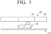
- a metal part 101 of a metal case 100 and an electronic circuit board 110 are connected to each other by using a contact terminal such as a C-clip 120 disposed on the electronic circuit board 110 as illustrated in FIG. 1 .
- a reference numeral 102 denotes a polymer insulating the metal pad 101.
- the metal which is currently mainly used as the material of the metal case 100 such as aluminum, magnesium, titanium, zinc, iron, stainless steel and the like
- a gold plated contact portion like the C-clip 120 disposed on the electronic circuit board 110 is in direct contact with the metal pad 101 of the metal part of the metal case 100 constituting an antenna, galvanic corrosion, fretting corrosion, or the like may occur, so that the antenna performance may be degraded or malfunction of the electronic device may occur due to contact failure.
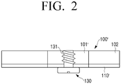
- a terminal portion of an electronic circuit board 110' and a metal pad 101' of a metal case 100' may be directly connected to each other with a screw 130 or a bolt.
- Such a structure may prevent galvanic corrosion or fretting corrosion from occurring in the terminal portion 101' of the metal case 100'.
- the electronic circuit board 110' is coupled to the metal case 100' by using the small screw 130 or bolt, a small screw hole 131 for screwing the screw 130 or the bolt is required to be machined on the metal pad 101' of the metal case 100'. Therefore, the machining cost may be increased, and a minimum thickness for the screw 130 or the bolt is required so that it may be limited to reduce the thickness of the metal case 100'.
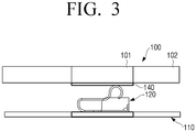
- a conductive tape 140 may be attached to a metal pad 101 of a metal case 100 so that the conductive tape 140 is positioned between the metal pad 101 of the metal case and a C-clip 120 of an electronic circuit board 110.
- the conductive tape 140 is composed of a conductive adhesive that can be attached to the metal pad and a film plated with one of gold, nickel, silver, and platinum.
- the conductive tape 140 has a problem that the reliability of the adhesive is low.
- the conductive tape 140 is attached to the metal pad of a small size of the metal case 100, there is a problem in that the metal case 100 using many metal pads 101 is poor in mass productivity.
- the conductive tape 140 having a thickness of 0.15 mm or more is provided between the metal case 100 and the C-clip 120 of the electronic circuit board 110, the thickness of the electronic device may be increased.
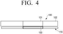
- a metal pad 101 of a metal case 100 and a terminal portion of an electronic circuit board 110 are connected to each other by using a double-sided conductive tape 150. Since such a method does not use a C-clip of the electronic circuit board 110, there is an advantage that the thickness of the joint portion may be reduced.
- the double-sided conductive tape 150 is attached to the metal pad of a small size of the metal case 100, there is a problem in that the metal case 100 using many metal pads is poor in mass productivity. Further, there is a problem in that repair is difficult when the electronic device is defective.
- An aspect of the present invention relates to an electronic device using a metal case having a structure capable of preventing galvanic corrosion or fretting corrosion from occurring when a metal member for connection such as a C-clip is used to connect an electronic circuit board and a metal pad of the metal case a part of which is used as an antenna or a part of an electronic circuit and a metal case used in the electronic device.
- an electronic device provided with a metal case may include a metal case in which at least one electronic circuit or antenna is formed; a metal pad provided on the metal case and electrically connected to the at least one electronic circuit or antenna; a metal sheet attached to a surface of the metal pad; and an electronic circuit board electrically connected to the at least one electronic circuit or antenna of the metal case through a metal member for connection detachably contacting the metal sheet.
- the metal pad and the metal sheet may be bonded to each other by ultrasonic welding or electric resistance welding.
- a plurality of bonding portions may be formed between the metal pad and the metal sheet.
- the plurality of bonding portions may be formed around a central portion of the metal sheet.
- the metal sheet may be formed in a rectangular shape, and corners of the metal sheet may be not provided with the plurality of bonding portions.
- the plurality of bonding portions may include a fusion portion formed by melting a melt of the metal pad and a metal of the metal sheet.
- the metal sheet may be fixed to the metal pad with a double-sided tape.
- the metal member for connection may be formed in any one of a C-clip, a spring, a conductive pin, and a conductive columnar structure.
- a portion of the metal member for connection contacting the metal sheet may be formed of one of gold, silver, platinum, tin, cobalt, copper, nickel, titanium, and the like or an alloy containing at least one of them.
- a portion of the metal member for connection contacting the metal sheet may be coated with one of gold, silver, platinum, tin, cobalt, copper, nickel, titanium, and the like.
- the metal sheet may be formed in a shape of a foil, a film, or a plate
- the metal sheet may be formed of one of gold, silver, platinum, tin, nickel, cobalt, titanium, and copper or an alloy containing at least one of them.
- a metal material including at least one of tin, zinc, silver, gold, indium, copper, bismuth, and nickel may be between the metal pad and the metal sheet.
- a metal case may include: the metal case including a metal part being used as at least one electronic circuit or antenna and a polymer; a metal pad provided on the metal part of the metal case; and a metal sheet attached to a surface of the metal pad, wherein the metal sheet may be bonded to the metal pad by ultrasonic welding or electric resistance welding.
- the metal sheet may be bonded to the metal pad by a plurality of bonding portions formed by the ultrasonic welding or the electric resistance welding.
- the plurality of bonding portions may be formed around a contact portion formed at a center of the metal sheet.
- the metal sheet may be temporarily fixed to the metal pad by a double-sided tape.
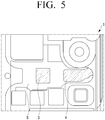
- FIG. 5 is a partial plan view illustrating a metal case according to an embodiment of the present disclosure in which a metal sheet is not disposed
- FIG. 6 is a partial cross-sectional view illustrating a state where a metal sheet is placed on a metal pad of the metal case of FIG. 5
- FIG. 7 is a partial plan view illustrating a metal case according to an embodiment of the present disclosure.
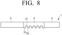
- FIG. 8 is a partial cross-sectional view illustrating the metal case of FIG. 7 according to the present disclosure taken along a line 8-8.
- a metal case 1 used in an electronic device according to an embodiment of the present disclosure is illustrated in FIG. 5 .
- the metal case 1 forms an appearance of the electronic device, and the metal case 1 may include a metal part and a polymer 5.
- An electronic circuit board 110 (see FIG. 13 ) may be provided below the metal case 1.
- the metal part may be formed as at least one electronic circuit or antenna.
- the electronic circuit or the antenna formed in the metal part needs to be electrically connected to the electronic circuit board 110.
- the metal part is provided with a metal pad 3 electrically connected to the electronic circuit or the antenna.
- the metal pad 3 may be provided in a number corresponding to the number of electronic circuits or antennas. For example, when four antennas are formed in the metal case 1 according to frequency bands, four metal pads 3 may be provided.
- the polymer 5 is placed between the plurality of electronic circuits or antennas so that the plurality of electronic circuits or antennas are insulated from each other.
- FIG. 5 is a view for showing two metal pads 3 and 4 exposed in the metal case 1.
- FIG. 5 is a partial plan view illustrating the metal case 1 of an electronic device, for example, the metal case 1 of a mobile electronic device in which a plurality of antennas are formed.
- the two metal pads 3 and 4 are electrically connected to the metal parts of the metal case 1 formed as the antennas or electronic circuits, respectively. Further, the two metal pads 3 and 4 are surrounded by non-conductive polymer 5 and are insulated from each other.
- the mobile electronic device may include a smartphone, a tablet computer, a notebook computer, a wearable device, and the like.
- FIG. 6 illustrates a state in which a metal sheet 10 is placed on the metal pad 3 of the metal case 1 of FIG. 5 , but the metal sheet 10 is not attached to the exposed surface of the metal pad 3 by ultrasonic welding or electric resistance welding.
- the metal sheet 10 is attached to the exposed surface of the metal pad 3 to prevent galvanic corrosion or fretting corrosion that occurs when the metal pad 3 is in directly contact with a metal member for connection 120 provided on the electronic circuit board 110.
- the metal sheet 10 may be formed in a shape corresponding to the metal pad 3 in the form of a foil, a film, or a plate.
- the metal sheet 10 may be formed in various shapes corresponding to the metal pad such as quadrangle, rectangle, square, circle, and the like.
- the metal sheet 10 is formed in a foil having a substantially square shape.
- the metal sheet 10 may be formed of at least one of metals such as gold, silver, platinum, tin, nickel, cobalt, copper, titanium, and the like, and alloys containing at least one of these metals.
- the metal sheet 10 may be formed by coating a metal plate having conductivity with the above-described metals.
- the metal sheet 10 may be formed by coating a copper plate with one of gold, silver, platinum, tin, nickel, and cobalt.
- the metal sheet 10 may be formed by coating one metal of gold, silver, platinum, nickel, tin and cobalt or an alloy containing at least one of these metals on a copper plate having a predetermined thickness in the range of 0.018 mm to 0.050 mm with one layer or a plurality of layers. At this time, the coating layer may be formed to have a thickness of 0.01 mm or less.
- the metal sheet 10 may be made of a metal having the same or superior corrosion resistance as and a strength similar to or stronger than the metal of the contact portion of the metal member for connection 120 of the electronic circuit board 110.
- FIG. 7 is a partial cross-sectional view illustrating a case where the metal sheet 10 of FIG. 6 is bonded to the metal pads 3 and 4 of the metal case 1.
- the metal sheet 10 is bonded to the metal pads 3 and 4 by ultrasonic welding or electric resistance welding.
- the metal sheet 10 and the metal pad 3 are bonded by a plurality of bonding portions 20 when the metal sheet 10 is bonded to the metal pad 3 by ultrasonic welding.
- the plurality of bonding portions 20 are formed in a concave groove shape as illustrated in FIG. 8 , respectively.
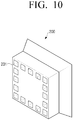
- the shape of each of the plurality of bonding portions 20 is formed in a shape corresponding to a plurality of protrusions 201 of an ultrasonic tool 200 as illustrated in FIG. 10 .
- the protrusions 201 of the ultrasonic tool 200 are formed in a substantially quadrangular pyramidal shape
- each of the plurality of bonding portions 20 is formed in a groove having a shape corresponding to the quadrangular pyramidal shape.
- each of the plurality of bonding portions 20 may include a fusion portion 21 in which the metal of the metal pad 3 and the metal of the metal sheet 10 are melted and interatomic bonding is generated.
- ultrasonic vibration is applied to the ultrasonic tool 200 as illustrated in FIG. 10 to form a plurality of concave bonding portions 20 on the metal sheet 10 so that the metal sheet 10 is bonded to the metal pad 3.
- the plurality of bonding portions 20 are arranged along the edge of the substantially square metal sheet 10 as illustrated in FIG. 7 , and the bonding portion 20 is not formed at the central portion 11.
- the plurality of bonding portions 20 are arranged along the edge of the circle and the bonding portion is not formed at the central portion.
- the central portion 11 of the metal sheet 10 without the bonding portion 20 is used as a contact region with which the metal member for connection 120 provided on the electronic circuit board 110 is in contact. Accordingly, the plurality of bonding portions 20 formed by ultrasonic welding are formed around the contact region 11 provided at the center of the metal sheet 10.
- the bonding portions 20 may not be formed at the corners of the metal sheet 10 as illustrated in FIG. 9 .
- FIG. 11a illustrates a case where a metal sheet 10' having a coating layer 10b in which one of gold, silver, platinum, tin, nickel, cobalt and titanium is coated on a top surface, a bottom surface or both surfaces of a conductive metal plate 10a such as a copper plate is bonded to the metal pad 3 of the metal case 1 by ultrasonic welding.
- the metal sheet 10' is bonded to the metal pad 3 by a plurality of bonding portions 20 formed by the ultrasonic welding.
- the plurality of bonding portions 20 may include a fusion portion 21' in which a part of a metal constituting the metal sheet 10 and a part of a metal constituting the metal pad 3 are fused with each other.
- FIG. 11b illustrates a case where a metal layer 10c is formed between the metal pad 3 of the metal case 1 and the metal sheet 10 in order to facilitate the bonding of the metal pad 3 and the metal sheet 10.
- the metal layer 10c may be formed of at least one metal of tin, zinc, silver, gold, copper, indium, bismuth and nickel or an alloy including at least one of these metals. Further, the metal layer 10c may be formed as a thin plate separately formed from the metal sheet 10 or may be formed as a coating layer on the exposed surface of the metal pad 3 or on one surface of the metal sheet 10. In the case of the present embodiment, the metal layer 10c is formed as a coating layer on the exposed surface of the metal pad 3.
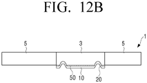
- FIG. 12a is a view illustrating a state in which the metal sheet 10 is temporarily attached to the metal pad 3 of the metal case 1 using a double-sided tape 50
- FIG. 12b is a view illustrating a state in which the metal sheet 10 of FIG. 12a is bonded to the metal pad 3 of the metal case 3 by ultrasonic welding.
- the metal sheet 10 When the metal sheet 10 is bonded to the metal pad 3 of the metal case 1 according to the present disclosure, before the metal sheet 10 is bonded to the metal pad 3 by ultrasonic welding, the metal sheet 10 may be temporarily fixed to the metal pad 3 with the double-sided tape 50 as illustrated in FIG. 12a so that the metal sheet 10 is stably attached to the metal pad 3 without falling off. If the metal sheet 10 is temporarily fixed with the double-sided tape 50 as described above, the metal sheet 10 may be prevented from moving relative to the metal pad 3 when ultrasonic welding is performed, thereby minimizing the occurrence of welding defects.
- the double-sided tape 50 does not exist in the plurality of bonding portions 20 for bonding the metal sheet 10 and the metal pad 3.
- the metal case 1 according to an embodiment of the present disclosure having the above-described structure may be used in various electronic devices.
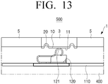
- FIG. 13 is a partial cross-sectional view conceptually illustrating an electronic device having a metal case according to an embodiment of the present disclosure.
- an electronic device 500 having a metal case may include a metal case 1 and an electronic circuit board 110.
- the metal case 1 may include a metal part where at least one electronic circuit or antenna is formed.
- the at least one electronic circuit may be a passage through which current flows or a passage for signal transmission.
- the at least one antenna may be formed so that a controller formed on the electronic circuit board 110 wirelessly communicates with an external device.
- the metal case 1 may be provided with a plurality of antennas corresponding to the plurality of frequency bands.
- the at least one electronic circuit or antenna provided in the metal case 1 may include a metal pad 3 electrically connected thereto.
- the metal pad 3 connects the electronic circuit board 110 formed separately from the metal case 1 and the at least one electronic circuit or antenna formed in the metal case 1 and may be formed of a conductive metal.
- the metal pad 3 is the same as the metal pad 3 of the metal case 1 as described above, and thus a detailed description thereof is omitted.
- the metal sheet 10 is attached to one surface of the metal pad 3, that is, the exposed surface of the metal pad 3.
- the metal sheet 10 is for preventing galvanic corrosion or fretting corrosion from occurring due to direct contact of the metal pad 3 with the metal member for connection 120 provided on the electronic circuit board 110, and is permanently bonded to the metal pad 3 by ultrasonic welding or electric resistance welding.
- the structure in which the metal sheet 10 is bonded to the metal pad 3 is the same as that of the metal case 1 as described above, so a detailed description of the bonding structure of the metal sheet 10 and the metal pad 3 is omitted.
- the electronic circuit board 110 is electrically connected to the at least one electronic circuit or antenna formed in the metal case 1.
- the metal member for connection 120 is provided on the electronic circuit board 110 to connect the electronic circuit board 110 to the metal case 1.
- the metal member for connection 120 electrically connects the at least one electronic circuit or antenna provided in the metal case 1 to the electronic circuit board 110, and is formed to be in detachably contact with the metal sheet 10 bonded to the metal pad 3 of the metal case 1.
- FIG. 13 illustrates a state in which the metal member for connection 120 is in contact with the metal sheet 10 of the metal case 1.
- the metal member for connection 120 provided on the electronic circuit board 110 may be formed in any one of a C-clip, a spring, a conductive pin, a conductive columnar structure.
- a C-clip is used as the metal member for connection 120.
- a contact portion 121 of the C-clip 120 is in elastically contact with the metal sheet 10 bonded to the metal case 1, so that the contact between the metal sheet 10 and the contact portion 121 of the C-clip 120 may be stably maintained.
- the metal member for connection 120 is formed of a metal having good electrical conductivity.
- the portion 121 which is in contact with the contact part 11 of the metal sheet 10 may be made of one metal of gold, silver, platinum, tin, cobalt, copper, nickel, titanium, and the like or an alloy containing at least one of these metals.
- the metal member for connection 120 may be formed of a metal having good electrical conductivity, and the contact portion 121 of the metal member for connection 120 which is in contact with the contact part 11 of the metal sheet 10 may be coated with one metal of gold, silver, platinum, tin, cobalt, copper, and the like.
- the electronic circuit board 110 may be formed variously according to the type of the electronic device 500.
- the electronic circuit board 110 when the electronic device 500 is a smartphone, the electronic circuit board 110 is disposed on the rear side of a display 400 and may be configured to perform functions of a general smartphone such as, for example, voice call, internet connection, application execution, photographing, and the like. At this time, the electronic circuit board 110 may be disposed between the metal case 1 and the display 400.
- the metal case 1 When the smartphone is connected to an external device through LTE, WiFi, Bluetooth, etc., the metal case 1 may be provided with an antenna for LTE connection, an antenna for WiFi connection, and an antenna for Bluetooth connection. They may be connected to the electronic circuit board 110 by the contact between the metal sheet 10 bonded to the metal pad 3 provided on each of them and the metal member for connection 120.
- the metal sheet bonded to the metal pad of the metal case is made of a metal having little or no potential difference from the metal of the contact portion of the metal member for connection provided on the electronic circuit board, galvanic corrosion may be prevented from occurring at the contact portion between the metal sheet and the metal member for connection.
- the metal sheet bonded to the metal pad of the metal case is made of a metal having the same or stronger strength as the metal of the contact portion of the metal member for connection provided on the electronic circuit board, fretting corrosion may be prevented from occurring at the contact portion between the metal sheet and the metal member for connection.
- the thin metal sheet is bonded to the metal pad of the metal case by ultrasonic welding or electric resistance welding. Therefore, the assembling work may be convenient and the electronic device may be made thinner compared to the prior art in which the metal case and the electronic circuit board are attached to each other using a bolt or a screw.
Landscapes
- Engineering & Computer Science (AREA)
- Microelectronics & Electronic Packaging (AREA)
- Telephone Set Structure (AREA)
- Casings For Electric Apparatus (AREA)
- Pressure Welding/Diffusion-Bonding (AREA)
- Computer Networks & Wireless Communication (AREA)
- Parts Printed On Printed Circuit Boards (AREA)
Applications Claiming Priority (2)
| Application Number | Priority Date | Filing Date | Title |
|---|---|---|---|
| KR1020150148911A KR102400529B1 (ko) | 2015-10-26 | 2015-10-26 | 금속 케이스를 구비한 전자기기 및 이에 사용되는 금속 케이스 |
| PCT/KR2016/008922 WO2017073893A1 (ko) | 2015-10-26 | 2016-08-16 | 금속 케이스를 구비한 전자기기 및 이에 사용되는 금속 케이스 |
Publications (3)
| Publication Number | Publication Date |
|---|---|
| EP3344022A1 true EP3344022A1 (de) | 2018-07-04 |
| EP3344022A4 EP3344022A4 (de) | 2018-08-29 |
| EP3344022B1 EP3344022B1 (de) | 2021-09-29 |
Family
ID=58630497
Family Applications (1)
| Application Number | Title | Priority Date | Filing Date |
|---|---|---|---|
| EP16860077.3A Not-in-force EP3344022B1 (de) | 2015-10-26 | 2016-08-16 | Elektronische vorrichtung mit metallgehäuse und metallgehäuse zur verwendung dafür |
Country Status (5)
| Country | Link |
|---|---|
| US (1) | US11291129B2 (de) |
| EP (1) | EP3344022B1 (de) |
| KR (1) | KR102400529B1 (de) |
| CN (1) | CN108141981B (de) |
| WO (1) | WO2017073893A1 (de) |
Cited By (2)
| Publication number | Priority date | Publication date | Assignee | Title |
|---|---|---|---|---|
| US11457528B2 (en) | 2019-06-05 | 2022-09-27 | Samsung Electronics Co., Ltd. | Electronic device having conductive structure of supporting member |
| US11455757B2 (en) | 2017-12-19 | 2022-09-27 | Samsung Electronics Co., Ltd. | Method and apparatus for reconstruction of original images from modified images |
Families Citing this family (13)
| Publication number | Priority date | Publication date | Assignee | Title |
|---|---|---|---|---|
| KR102527317B1 (ko) | 2016-08-30 | 2023-05-03 | 삼성전자주식회사 | 금속 패드가 부착된 금속 케이스를 구비한 전자기기 |
| KR102591783B1 (ko) * | 2018-10-16 | 2023-10-23 | 삼성전자주식회사 | 디스플레이 장치 |
| KR102621845B1 (ko) * | 2019-03-26 | 2024-01-08 | 삼성전자주식회사 | 안테나 접속 부재를 포함하는 전자 장치 |
| KR102711476B1 (ko) * | 2020-02-03 | 2024-09-27 | 삼성전자주식회사 | 인쇄 회로 기판을 포함하는 전자 장치 |
| TWI729965B (zh) * | 2020-12-04 | 2021-06-01 | 財團法人金屬工業研究發展中心 | 複合積層板、殼體及行動通訊裝置 |
| EP4254723A4 (de) * | 2021-03-18 | 2024-07-17 | Samsung Electronics Co., Ltd. | Elektronische vorrichtung mit antennenelement zum drahtlosen laden |
| CN115190713B (zh) * | 2021-04-02 | 2024-06-25 | 成都鼎桥通信技术有限公司 | 防腐蚀通信设备的外壳和通信设备 |
| CN113423217B (zh) * | 2021-06-18 | 2022-12-06 | Oppo广东移动通信有限公司 | 壳体组件的成型方法、壳体组件及电子设备 |
| US12133342B2 (en) | 2021-07-23 | 2024-10-29 | Samsung Electronics Co., Ltd. | Electronic device including a conductive portion and contact member making contact with substrate |
| KR20230015752A (ko) * | 2021-07-23 | 2023-01-31 | 삼성전자주식회사 | 전자 장치 |
| CN115811848B (zh) * | 2021-09-13 | 2025-09-05 | 华为技术有限公司 | 镁合金连接结构件、电子设备和构件成型方法 |
| CN117715327A (zh) * | 2022-09-06 | 2024-03-15 | 苏州佳世达电通有限公司 | 可自动切换其操作模式的电子装置 |
| WO2026095343A1 (ko) * | 2024-10-31 | 2026-05-07 | 삼성전자 주식회사 | 전도성 접촉 부재를 포함하는 전자 장치 |
Family Cites Families (23)
| Publication number | Priority date | Publication date | Assignee | Title |
|---|---|---|---|---|
| US3439231A (en) * | 1967-02-13 | 1969-04-15 | Mallory & Co Inc P R | Hermetically encapsulated electronic device |
| US5772451A (en) * | 1993-11-16 | 1998-06-30 | Form Factor, Inc. | Sockets for electronic components and methods of connecting to electronic components |
| US6563042B2 (en) * | 1999-05-21 | 2003-05-13 | Intel Corporation | Radiating enclosure |
| JP2001298259A (ja) | 2000-04-17 | 2001-10-26 | Sharp Corp | 電気部品の接続方法 |
| US6544047B2 (en) | 2001-03-30 | 2003-04-08 | Intel Corporation | Dual-swiping interconnection clip, and hook and slot arrangement for printed circuit board (PCB) attachment |
| KR101161722B1 (ko) * | 2004-05-20 | 2012-07-06 | 가부시키가이샤 한도오따이 에네루기 켄큐쇼 | 발광소자 및 표시장치 |
| KR100593945B1 (ko) * | 2005-05-30 | 2006-06-30 | 삼성전기주식회사 | 고출력 led 패키지 및 그 제조방법 |
| JP4508025B2 (ja) * | 2005-07-26 | 2010-07-21 | セイコーエプソン株式会社 | ラインヘッド、ラインヘッドモジュール、及び画像形成装置 |
| KR101151125B1 (ko) * | 2007-08-27 | 2012-06-01 | 가부시키가이샤 히타치세이사쿠쇼 | 반도체 왜곡 센서 |
| CN101471520A (zh) * | 2007-12-25 | 2009-07-01 | 英业达股份有限公司 | 整合电源导电模组的壳体结构及其应用的电子装置 |
| JP2009200236A (ja) | 2008-02-21 | 2009-09-03 | Daisho Denshi Co Ltd | 接触端子付き基板、icメモリーカード、接触端子付き基板の製造方法 |
| KR101552155B1 (ko) | 2009-06-25 | 2015-09-10 | 엘지전자 주식회사 | 이동 단말기 |
| KR101123515B1 (ko) | 2010-02-26 | 2012-03-12 | 엘에스엠트론 주식회사 | 접속 구조가 개선된 내장형 안테나 |
| JP2012044008A (ja) * | 2010-08-20 | 2012-03-01 | Ii P I:Kk | 回路基板、その製造方法、及び、接続構造 |
| JP5788166B2 (ja) | 2010-11-02 | 2015-09-30 | 新光電気工業株式会社 | 接続端子構造及びその製造方法、並びにソケット |
| KR101486479B1 (ko) | 2011-08-01 | 2015-02-06 | 플라텔코퍼레이션(주) | 이동통신 단말기용 케이스 안테나 및 그를 채용한 이동통신 단말기 |
| KR101394459B1 (ko) | 2012-05-17 | 2014-05-13 | (주)파트론 | 안테나 구조체 및 이의 제조 방법 |
| KR101973127B1 (ko) | 2012-11-13 | 2019-04-26 | 삼성전자주식회사 | 휴대용 단말기의 안테나 장치 |
| CN105052042B (zh) * | 2013-07-05 | 2017-07-11 | Lg 电子株式会社 | 移动终端 |
| KR20150017179A (ko) * | 2013-08-06 | 2015-02-16 | 삼성전자주식회사 | 안테나 장치 및 그것을 갖는 전자 장치 |
| US9583821B2 (en) | 2013-09-04 | 2017-02-28 | Apple Inc. | Antenna related features of a mobile phone or computing device |
| KR20150045180A (ko) | 2013-10-18 | 2015-04-28 | 엘지전자 주식회사 | 이동 단말기 |
| CN104934690B (zh) * | 2015-05-06 | 2017-09-05 | 东莞劲胜精密组件股份有限公司 | 制备天线连接结构的方法和天线连接结构及移动通讯终端 |
-
2015
- 2015-10-26 KR KR1020150148911A patent/KR102400529B1/ko active Active
-
2016
- 2016-08-16 EP EP16860077.3A patent/EP3344022B1/de not_active Not-in-force
- 2016-08-16 WO PCT/KR2016/008922 patent/WO2017073893A1/ko not_active Ceased
- 2016-08-16 CN CN201680060982.0A patent/CN108141981B/zh active Active
- 2016-08-16 US US15/769,436 patent/US11291129B2/en active Active
Cited By (2)
| Publication number | Priority date | Publication date | Assignee | Title |
|---|---|---|---|---|
| US11455757B2 (en) | 2017-12-19 | 2022-09-27 | Samsung Electronics Co., Ltd. | Method and apparatus for reconstruction of original images from modified images |
| US11457528B2 (en) | 2019-06-05 | 2022-09-27 | Samsung Electronics Co., Ltd. | Electronic device having conductive structure of supporting member |
Also Published As
| Publication number | Publication date |
|---|---|
| EP3344022B1 (de) | 2021-09-29 |
| EP3344022A4 (de) | 2018-08-29 |
| US20180310423A1 (en) | 2018-10-25 |
| KR102400529B1 (ko) | 2022-05-20 |
| CN108141981A (zh) | 2018-06-08 |
| CN108141981B (zh) | 2020-12-25 |
| US11291129B2 (en) | 2022-03-29 |
| WO2017073893A1 (ko) | 2017-05-04 |
| KR20170048043A (ko) | 2017-05-08 |
Similar Documents
| Publication | Publication Date | Title |
|---|---|---|
| EP3344022B1 (de) | Elektronische vorrichtung mit metallgehäuse und metallgehäuse zur verwendung dafür | |
| CN107003538B (zh) | 集成照相机镜头悬置器 | |
| US9787011B2 (en) | Surface mounting contact member | |
| KR20180002478A (ko) | 탄성 전기접촉단자 | |
| US20160027751A1 (en) | Semiconductor device having solder joint and method of forming the same | |
| US10034373B2 (en) | Circuit board secured to battery cell using a circuit board through hole and methods for welding the circuit board | |
| US11374306B2 (en) | Electronic device comprising metal case having metal pad attached thereto | |
| KR102183030B1 (ko) | 전기접촉단자의 장착 구조 | |
| CN210167512U (zh) | 镁合金结构件和终端 | |
| CN107251339A (zh) | 弹性连接器 | |
| US9570827B2 (en) | Contact member | |
| WO2019230333A1 (ja) | 配線回路基板 | |
| CN209843955U (zh) | 一种电子设备 | |
| CN110265762B (zh) | 电子设备及其制备方法 | |
| JP6896097B2 (ja) | スイッチ用可動接点体及びスイッチ | |
| CN116887551A (zh) | 电子设备 | |
| JP4952438B2 (ja) | 温度ヒューズ | |
| JP4998146B2 (ja) | 温度ヒューズ | |
| CN221263495U (zh) | 一种应用于sensor-shift马达中的悬架板结构 | |
| JP2013026140A (ja) | 弾性コネクタ | |
| CN210984954U (zh) | 一种高稳定性的柔性天线 | |
| US20190239354A1 (en) | Metal pad interface | |
| EP2825003A1 (de) | Leiterplatte und Elektrowerkzeugschalter damit | |
| JP2015201570A (ja) | チップ型抵抗器及びその製造方法 | |
| EP3012881B1 (de) | Verfahren zur herstellung einer struktur für flexible leiterplatten |
Legal Events
| Date | Code | Title | Description |
|---|---|---|---|
| STAA | Information on the status of an ep patent application or granted ep patent |
Free format text: STATUS: THE INTERNATIONAL PUBLICATION HAS BEEN MADE |
|
| PUAI | Public reference made under article 153(3) epc to a published international application that has entered the european phase |
Free format text: ORIGINAL CODE: 0009012 |
|
| STAA | Information on the status of an ep patent application or granted ep patent |
Free format text: STATUS: REQUEST FOR EXAMINATION WAS MADE |
|
| 17P | Request for examination filed |
Effective date: 20180329 |
|
| AK | Designated contracting states |
Kind code of ref document: A1 Designated state(s): AL AT BE BG CH CY CZ DE DK EE ES FI FR GB GR HR HU IE IS IT LI LT LU LV MC MK MT NL NO PL PT RO RS SE SI SK SM TR |
|
| AX | Request for extension of the european patent |
Extension state: BA ME |
|
| A4 | Supplementary search report drawn up and despatched |
Effective date: 20180727 |
|
| RIC1 | Information provided on ipc code assigned before grant |
Ipc: H01Q 1/24 20060101ALI20180723BHEP Ipc: H05K 5/04 20060101AFI20180723BHEP Ipc: B32B 15/08 20060101ALI20180723BHEP Ipc: H01R 13/03 20060101ALI20180723BHEP Ipc: H01R 13/24 20060101ALI20180723BHEP |
|
| DAV | Request for validation of the european patent (deleted) | ||
| DAX | Request for extension of the european patent (deleted) | ||
| STAA | Information on the status of an ep patent application or granted ep patent |
Free format text: STATUS: EXAMINATION IS IN PROGRESS |
|
| 17Q | First examination report despatched |
Effective date: 20190516 |
|
| RIC1 | Information provided on ipc code assigned before grant |
Ipc: H01Q 1/24 20060101AFI20201218BHEP Ipc: H01R 13/03 20060101ALI20201218BHEP Ipc: H05K 5/04 20060101ALI20201218BHEP Ipc: B32B 15/08 20060101ALI20201218BHEP Ipc: H01R 13/24 20060101ALI20201218BHEP Ipc: H01R 43/02 20060101ALI20201218BHEP |
|
| REG | Reference to a national code |
Ref country code: DE Ref legal event code: R079 Ref document number: 602016064457 Country of ref document: DE Free format text: PREVIOUS MAIN CLASS: H05K0005040000 Ipc: H01Q0001240000 |
|
| GRAP | Despatch of communication of intention to grant a patent |
Free format text: ORIGINAL CODE: EPIDOSNIGR1 |
|
| STAA | Information on the status of an ep patent application or granted ep patent |
Free format text: STATUS: GRANT OF PATENT IS INTENDED |
|
| RIC1 | Information provided on ipc code assigned before grant |
Ipc: H01R 43/02 20060101ALN20210309BHEP Ipc: H01Q 1/24 20060101AFI20210309BHEP |
|
| INTG | Intention to grant announced |
Effective date: 20210322 |
|
| GRAS | Grant fee paid |
Free format text: ORIGINAL CODE: EPIDOSNIGR3 |
|
| GRAA | (expected) grant |
Free format text: ORIGINAL CODE: 0009210 |
|
| STAA | Information on the status of an ep patent application or granted ep patent |
Free format text: STATUS: THE PATENT HAS BEEN GRANTED |
|
| AK | Designated contracting states |
Kind code of ref document: B1 Designated state(s): AL AT BE BG CH CY CZ DE DK EE ES FI FR GB GR HR HU IE IS IT LI LT LU LV MC MK MT NL NO PL PT RO RS SE SI SK SM TR |
|
| REG | Reference to a national code |
Ref country code: GB Ref legal event code: FG4D |
|
| REG | Reference to a national code |
Ref country code: CH Ref legal event code: EP Ref country code: AT Ref legal event code: REF Ref document number: 1435015 Country of ref document: AT Kind code of ref document: T Effective date: 20211015 |
|
| REG | Reference to a national code |
Ref country code: DE Ref legal event code: R096 Ref document number: 602016064457 Country of ref document: DE |
|
| REG | Reference to a national code |
Ref country code: IE Ref legal event code: FG4D |
|
| REG | Reference to a national code |
Ref country code: LT Ref legal event code: MG9D |
|
| PG25 | Lapsed in a contracting state [announced via postgrant information from national office to epo] |
Ref country code: RS Free format text: LAPSE BECAUSE OF FAILURE TO SUBMIT A TRANSLATION OF THE DESCRIPTION OR TO PAY THE FEE WITHIN THE PRESCRIBED TIME-LIMIT Effective date: 20210929 Ref country code: SE Free format text: LAPSE BECAUSE OF FAILURE TO SUBMIT A TRANSLATION OF THE DESCRIPTION OR TO PAY THE FEE WITHIN THE PRESCRIBED TIME-LIMIT Effective date: 20210929 Ref country code: NO Free format text: LAPSE BECAUSE OF FAILURE TO SUBMIT A TRANSLATION OF THE DESCRIPTION OR TO PAY THE FEE WITHIN THE PRESCRIBED TIME-LIMIT Effective date: 20211229 Ref country code: FI Free format text: LAPSE BECAUSE OF FAILURE TO SUBMIT A TRANSLATION OF THE DESCRIPTION OR TO PAY THE FEE WITHIN THE PRESCRIBED TIME-LIMIT Effective date: 20210929 Ref country code: HR Free format text: LAPSE BECAUSE OF FAILURE TO SUBMIT A TRANSLATION OF THE DESCRIPTION OR TO PAY THE FEE WITHIN THE PRESCRIBED TIME-LIMIT Effective date: 20210929 Ref country code: BG Free format text: LAPSE BECAUSE OF FAILURE TO SUBMIT A TRANSLATION OF THE DESCRIPTION OR TO PAY THE FEE WITHIN THE PRESCRIBED TIME-LIMIT Effective date: 20211229 Ref country code: LT Free format text: LAPSE BECAUSE OF FAILURE TO SUBMIT A TRANSLATION OF THE DESCRIPTION OR TO PAY THE FEE WITHIN THE PRESCRIBED TIME-LIMIT Effective date: 20210929 |
|
| REG | Reference to a national code |
Ref country code: NL Ref legal event code: MP Effective date: 20210929 |
|
| REG | Reference to a national code |
Ref country code: AT Ref legal event code: MK05 Ref document number: 1435015 Country of ref document: AT Kind code of ref document: T Effective date: 20210929 |
|
| PG25 | Lapsed in a contracting state [announced via postgrant information from national office to epo] |
Ref country code: LV Free format text: LAPSE BECAUSE OF FAILURE TO SUBMIT A TRANSLATION OF THE DESCRIPTION OR TO PAY THE FEE WITHIN THE PRESCRIBED TIME-LIMIT Effective date: 20210929 Ref country code: GR Free format text: LAPSE BECAUSE OF FAILURE TO SUBMIT A TRANSLATION OF THE DESCRIPTION OR TO PAY THE FEE WITHIN THE PRESCRIBED TIME-LIMIT Effective date: 20211230 |
|
| PG25 | Lapsed in a contracting state [announced via postgrant information from national office to epo] |
Ref country code: AT Free format text: LAPSE BECAUSE OF FAILURE TO SUBMIT A TRANSLATION OF THE DESCRIPTION OR TO PAY THE FEE WITHIN THE PRESCRIBED TIME-LIMIT Effective date: 20210929 |
|
| PG25 | Lapsed in a contracting state [announced via postgrant information from national office to epo] |
Ref country code: IS Free format text: LAPSE BECAUSE OF FAILURE TO SUBMIT A TRANSLATION OF THE DESCRIPTION OR TO PAY THE FEE WITHIN THE PRESCRIBED TIME-LIMIT Effective date: 20220129 Ref country code: SK Free format text: LAPSE BECAUSE OF FAILURE TO SUBMIT A TRANSLATION OF THE DESCRIPTION OR TO PAY THE FEE WITHIN THE PRESCRIBED TIME-LIMIT Effective date: 20210929 Ref country code: RO Free format text: LAPSE BECAUSE OF FAILURE TO SUBMIT A TRANSLATION OF THE DESCRIPTION OR TO PAY THE FEE WITHIN THE PRESCRIBED TIME-LIMIT Effective date: 20210929 Ref country code: PT Free format text: LAPSE BECAUSE OF FAILURE TO SUBMIT A TRANSLATION OF THE DESCRIPTION OR TO PAY THE FEE WITHIN THE PRESCRIBED TIME-LIMIT Effective date: 20220131 Ref country code: PL Free format text: LAPSE BECAUSE OF FAILURE TO SUBMIT A TRANSLATION OF THE DESCRIPTION OR TO PAY THE FEE WITHIN THE PRESCRIBED TIME-LIMIT Effective date: 20210929 Ref country code: NL Free format text: LAPSE BECAUSE OF FAILURE TO SUBMIT A TRANSLATION OF THE DESCRIPTION OR TO PAY THE FEE WITHIN THE PRESCRIBED TIME-LIMIT Effective date: 20210929 Ref country code: ES Free format text: LAPSE BECAUSE OF FAILURE TO SUBMIT A TRANSLATION OF THE DESCRIPTION OR TO PAY THE FEE WITHIN THE PRESCRIBED TIME-LIMIT Effective date: 20210929 Ref country code: EE Free format text: LAPSE BECAUSE OF FAILURE TO SUBMIT A TRANSLATION OF THE DESCRIPTION OR TO PAY THE FEE WITHIN THE PRESCRIBED TIME-LIMIT Effective date: 20210929 Ref country code: CZ Free format text: LAPSE BECAUSE OF FAILURE TO SUBMIT A TRANSLATION OF THE DESCRIPTION OR TO PAY THE FEE WITHIN THE PRESCRIBED TIME-LIMIT Effective date: 20210929 Ref country code: AL Free format text: LAPSE BECAUSE OF FAILURE TO SUBMIT A TRANSLATION OF THE DESCRIPTION OR TO PAY THE FEE WITHIN THE PRESCRIBED TIME-LIMIT Effective date: 20210929 |
|
| REG | Reference to a national code |
Ref country code: DE Ref legal event code: R097 Ref document number: 602016064457 Country of ref document: DE |
|
| PG25 | Lapsed in a contracting state [announced via postgrant information from national office to epo] |
Ref country code: DK Free format text: LAPSE BECAUSE OF FAILURE TO SUBMIT A TRANSLATION OF THE DESCRIPTION OR TO PAY THE FEE WITHIN THE PRESCRIBED TIME-LIMIT Effective date: 20210929 |
|
| PLBE | No opposition filed within time limit |
Free format text: ORIGINAL CODE: 0009261 |
|
| STAA | Information on the status of an ep patent application or granted ep patent |
Free format text: STATUS: NO OPPOSITION FILED WITHIN TIME LIMIT |
|
| 26N | No opposition filed |
Effective date: 20220630 |
|
| PG25 | Lapsed in a contracting state [announced via postgrant information from national office to epo] |
Ref country code: SI Free format text: LAPSE BECAUSE OF FAILURE TO SUBMIT A TRANSLATION OF THE DESCRIPTION OR TO PAY THE FEE WITHIN THE PRESCRIBED TIME-LIMIT Effective date: 20210929 |
|
| PG25 | Lapsed in a contracting state [announced via postgrant information from national office to epo] |
Ref country code: IT Free format text: LAPSE BECAUSE OF FAILURE TO SUBMIT A TRANSLATION OF THE DESCRIPTION OR TO PAY THE FEE WITHIN THE PRESCRIBED TIME-LIMIT Effective date: 20210929 |
|
| REG | Reference to a national code |
Ref country code: DE Ref legal event code: R119 Ref document number: 602016064457 Country of ref document: DE |
|
| PG25 | Lapsed in a contracting state [announced via postgrant information from national office to epo] |
Ref country code: MC Free format text: LAPSE BECAUSE OF FAILURE TO SUBMIT A TRANSLATION OF THE DESCRIPTION OR TO PAY THE FEE WITHIN THE PRESCRIBED TIME-LIMIT Effective date: 20210929 |
|
| REG | Reference to a national code |
Ref country code: CH Ref legal event code: PL |
|
| GBPC | Gb: european patent ceased through non-payment of renewal fee |
Effective date: 20220816 |
|
| PG25 | Lapsed in a contracting state [announced via postgrant information from national office to epo] |
Ref country code: LU Free format text: LAPSE BECAUSE OF NON-PAYMENT OF DUE FEES Effective date: 20220816 Ref country code: LI Free format text: LAPSE BECAUSE OF NON-PAYMENT OF DUE FEES Effective date: 20220831 Ref country code: CH Free format text: LAPSE BECAUSE OF NON-PAYMENT OF DUE FEES Effective date: 20220831 |
|
| REG | Reference to a national code |
Ref country code: BE Ref legal event code: MM Effective date: 20220831 |
|
| PG25 | Lapsed in a contracting state [announced via postgrant information from national office to epo] |
Ref country code: IE Free format text: LAPSE BECAUSE OF NON-PAYMENT OF DUE FEES Effective date: 20220816 Ref country code: FR Free format text: LAPSE BECAUSE OF NON-PAYMENT OF DUE FEES Effective date: 20220831 Ref country code: DE Free format text: LAPSE BECAUSE OF NON-PAYMENT OF DUE FEES Effective date: 20230301 |
|
| PG25 | Lapsed in a contracting state [announced via postgrant information from national office to epo] |
Ref country code: BE Free format text: LAPSE BECAUSE OF NON-PAYMENT OF DUE FEES Effective date: 20220831 |
|
| PG25 | Lapsed in a contracting state [announced via postgrant information from national office to epo] |
Ref country code: GB Free format text: LAPSE BECAUSE OF NON-PAYMENT OF DUE FEES Effective date: 20220816 |
|
| PG25 | Lapsed in a contracting state [announced via postgrant information from national office to epo] |
Ref country code: HU Free format text: LAPSE BECAUSE OF FAILURE TO SUBMIT A TRANSLATION OF THE DESCRIPTION OR TO PAY THE FEE WITHIN THE PRESCRIBED TIME-LIMIT; INVALID AB INITIO Effective date: 20160816 |
|
| PG25 | Lapsed in a contracting state [announced via postgrant information from national office to epo] |
Ref country code: SM Free format text: LAPSE BECAUSE OF FAILURE TO SUBMIT A TRANSLATION OF THE DESCRIPTION OR TO PAY THE FEE WITHIN THE PRESCRIBED TIME-LIMIT Effective date: 20210929 Ref country code: CY Free format text: LAPSE BECAUSE OF FAILURE TO SUBMIT A TRANSLATION OF THE DESCRIPTION OR TO PAY THE FEE WITHIN THE PRESCRIBED TIME-LIMIT Effective date: 20210929 |
|
| PG25 | Lapsed in a contracting state [announced via postgrant information from national office to epo] |
Ref country code: MK Free format text: LAPSE BECAUSE OF FAILURE TO SUBMIT A TRANSLATION OF THE DESCRIPTION OR TO PAY THE FEE WITHIN THE PRESCRIBED TIME-LIMIT Effective date: 20210929 |
|
| PG25 | Lapsed in a contracting state [announced via postgrant information from national office to epo] |
Ref country code: TR Free format text: LAPSE BECAUSE OF FAILURE TO SUBMIT A TRANSLATION OF THE DESCRIPTION OR TO PAY THE FEE WITHIN THE PRESCRIBED TIME-LIMIT Effective date: 20210929 |
|
| PG25 | Lapsed in a contracting state [announced via postgrant information from national office to epo] |
Ref country code: MT Free format text: LAPSE BECAUSE OF FAILURE TO SUBMIT A TRANSLATION OF THE DESCRIPTION OR TO PAY THE FEE WITHIN THE PRESCRIBED TIME-LIMIT Effective date: 20210929 |